EP2721680B1 - Fuel cell system with interconnect - Google Patents
Fuel cell system with interconnect Download PDFInfo
- Publication number
- EP2721680B1 EP2721680B1 EP12800291.2A EP12800291A EP2721680B1 EP 2721680 B1 EP2721680 B1 EP 2721680B1 EP 12800291 A EP12800291 A EP 12800291A EP 2721680 B1 EP2721680 B1 EP 2721680B1
- Authority
- EP
- European Patent Office
- Prior art keywords
- interconnect
- cathode
- anode
- fuel cell
- conductor
- Prior art date
- Legal status (The legal status is an assumption and is not a legal conclusion. Google has not performed a legal analysis and makes no representation as to the accuracy of the status listed.)
- Not-in-force
Links
- 239000000446 fuel Substances 0.000 title claims description 202
- 239000003792 electrolyte Substances 0.000 claims description 148
- 239000000919 ceramic Substances 0.000 claims description 137
- 239000000758 substrate Substances 0.000 claims description 97
- 238000009792 diffusion process Methods 0.000 claims description 54
- 239000011195 cermet Substances 0.000 claims description 40
- 239000012212 insulator Substances 0.000 claims description 29
- 239000010970 precious metal Substances 0.000 claims description 29
- -1 Pr2Zr2O7 Inorganic materials 0.000 claims description 22
- 238000000926 separation method Methods 0.000 claims description 19
- 229910014031 strontium zirconium oxide Inorganic materials 0.000 claims description 13
- TWNQGVIAIRXVLR-UHFFFAOYSA-N oxo(oxoalumanyloxy)alumane Chemical group O=[Al]O[Al]=O TWNQGVIAIRXVLR-UHFFFAOYSA-N 0.000 claims description 11
- 229910002230 La2Zr2O7 Inorganic materials 0.000 claims description 9
- 239000001301 oxygen Substances 0.000 claims description 7
- 229910052760 oxygen Inorganic materials 0.000 claims description 7
- QVGXLLKOCUKJST-UHFFFAOYSA-N atomic oxygen Chemical compound [O] QVGXLLKOCUKJST-UHFFFAOYSA-N 0.000 claims description 5
- 230000008878 coupling Effects 0.000 claims description 4
- 238000010168 coupling process Methods 0.000 claims description 4
- 238000005859 coupling reaction Methods 0.000 claims description 4
- 239000004020 conductor Substances 0.000 description 329
- 210000004027 cell Anatomy 0.000 description 244
- 239000010408 film Substances 0.000 description 123
- 239000000463 material Substances 0.000 description 122
- 239000000126 substance Substances 0.000 description 86
- 230000004888 barrier function Effects 0.000 description 85
- 239000012071 phase Substances 0.000 description 54
- 229910001233 yttria-stabilized zirconia Inorganic materials 0.000 description 48
- 239000000203 mixture Substances 0.000 description 40
- 230000000670 limiting effect Effects 0.000 description 36
- 239000007800 oxidant agent Substances 0.000 description 31
- MCMNRKCIXSYSNV-UHFFFAOYSA-N Zirconium dioxide Chemical compound O=[Zr]=O MCMNRKCIXSYSNV-UHFFFAOYSA-N 0.000 description 29
- 230000001590 oxidative effect Effects 0.000 description 28
- 229910052763 palladium Inorganic materials 0.000 description 26
- 229910052596 spinel Inorganic materials 0.000 description 26
- 230000005012 migration Effects 0.000 description 23
- 238000013508 migration Methods 0.000 description 23
- PXHVJJICTQNCMI-UHFFFAOYSA-N nickel Substances [Ni] PXHVJJICTQNCMI-UHFFFAOYSA-N 0.000 description 23
- 238000012360 testing method Methods 0.000 description 23
- 239000007789 gas Substances 0.000 description 21
- 230000003071 parasitic effect Effects 0.000 description 19
- GWEVSGVZZGPLCZ-UHFFFAOYSA-N Titan oxide Chemical compound O=[Ti]=O GWEVSGVZZGPLCZ-UHFFFAOYSA-N 0.000 description 18
- 239000007788 liquid Substances 0.000 description 18
- 229910052697 platinum Inorganic materials 0.000 description 18
- 229910026161 MgAl2O4 Inorganic materials 0.000 description 17
- 238000010304 firing Methods 0.000 description 16
- 229910045601 alloy Inorganic materials 0.000 description 15
- 239000000956 alloy Substances 0.000 description 15
- 229910009474 Y2O3—ZrO2 Inorganic materials 0.000 description 14
- CETPSERCERDGAM-UHFFFAOYSA-N ceric oxide Chemical compound O=[Ce]=O CETPSERCERDGAM-UHFFFAOYSA-N 0.000 description 14
- 229910000422 cerium(IV) oxide Inorganic materials 0.000 description 14
- 229910001404 rare earth metal oxide Inorganic materials 0.000 description 14
- LEMJVPWNQLQFLW-UHFFFAOYSA-N [La+3].[La+3].[O-][Cr]([O-])=O.[O-][Cr]([O-])=O.[O-][Cr]([O-])=O Chemical class [La+3].[La+3].[O-][Cr]([O-])=O.[O-][Cr]([O-])=O.[O-][Cr]([O-])=O LEMJVPWNQLQFLW-UHFFFAOYSA-N 0.000 description 10
- PNEYBMLMFCGWSK-UHFFFAOYSA-N aluminium oxide Inorganic materials [O-2].[O-2].[O-2].[Al+3].[Al+3] PNEYBMLMFCGWSK-UHFFFAOYSA-N 0.000 description 10
- 230000015572 biosynthetic process Effects 0.000 description 10
- 230000007547 defect Effects 0.000 description 10
- 238000013461 design Methods 0.000 description 10
- 229910052737 gold Inorganic materials 0.000 description 10
- 230000004048 modification Effects 0.000 description 10
- 238000012986 modification Methods 0.000 description 10
- 229910052709 silver Inorganic materials 0.000 description 10
- 230000015556 catabolic process Effects 0.000 description 9
- 238000006731 degradation reaction Methods 0.000 description 9
- 238000000034 method Methods 0.000 description 9
- 239000011029 spinel Substances 0.000 description 9
- VEALVRVVWBQVSL-UHFFFAOYSA-N strontium titanate Chemical compound [Sr+2].[O-][Ti]([O-])=O VEALVRVVWBQVSL-UHFFFAOYSA-N 0.000 description 9
- 229910002080 8 mol% Y2O3 fully stabilized ZrO2 Inorganic materials 0.000 description 8
- ROKHXTDWQPQQEO-UHFFFAOYSA-N [Y+3].[Y+3].[O-][Cr]([O-])=O.[O-][Cr]([O-])=O.[O-][Cr]([O-])=O Chemical class [Y+3].[Y+3].[O-][Cr]([O-])=O.[O-][Cr]([O-])=O.[O-][Cr]([O-])=O ROKHXTDWQPQQEO-UHFFFAOYSA-N 0.000 description 8
- 238000001218 confocal laser scanning microscopy Methods 0.000 description 8
- 239000000976 ink Substances 0.000 description 8
- 229910052688 Gadolinium Inorganic materials 0.000 description 7
- 229910000990 Ni alloy Inorganic materials 0.000 description 7
- 241000968352 Scandia <hydrozoan> Species 0.000 description 7
- 239000001257 hydrogen Substances 0.000 description 7
- 229910052739 hydrogen Inorganic materials 0.000 description 7
- HJGMWXTVGKLUAQ-UHFFFAOYSA-N oxygen(2-);scandium(3+) Chemical compound [O-2].[O-2].[O-2].[Sc+3].[Sc+3] HJGMWXTVGKLUAQ-UHFFFAOYSA-N 0.000 description 7
- RUDFQVOCFDJEEF-UHFFFAOYSA-N yttrium(III) oxide Inorganic materials [O-2].[O-2].[O-2].[Y+3].[Y+3] RUDFQVOCFDJEEF-UHFFFAOYSA-N 0.000 description 7
- UFHFLCQGNIYNRP-UHFFFAOYSA-N Hydrogen Chemical compound [H][H] UFHFLCQGNIYNRP-UHFFFAOYSA-N 0.000 description 6
- 229910052772 Samarium Inorganic materials 0.000 description 6
- 229910010293 ceramic material Inorganic materials 0.000 description 6
- 229910052746 lanthanum Inorganic materials 0.000 description 6
- 239000002184 metal Substances 0.000 description 6
- 229910002119 nickel–yttria stabilized zirconia Inorganic materials 0.000 description 6
- 238000005325 percolation Methods 0.000 description 6
- 238000012545 processing Methods 0.000 description 6
- 239000000376 reactant Substances 0.000 description 6
- 230000002829 reductive effect Effects 0.000 description 6
- 238000007650 screen-printing Methods 0.000 description 6
- 229910052691 Erbium Inorganic materials 0.000 description 5
- 229910052689 Holmium Inorganic materials 0.000 description 5
- 229910002127 La0.6Sr0.4Co0.2Fe0.8O3 Inorganic materials 0.000 description 5
- 229910052779 Neodymium Inorganic materials 0.000 description 5
- 229910052777 Praseodymium Inorganic materials 0.000 description 5
- 230000008569 process Effects 0.000 description 5
- 229910052761 rare earth metal Inorganic materials 0.000 description 5
- 229910002710 Au-Pd Inorganic materials 0.000 description 4
- 230000006870 function Effects 0.000 description 4
- MRELNEQAGSRDBK-UHFFFAOYSA-N lanthanum oxide Inorganic materials [O-2].[O-2].[O-2].[La+3].[La+3] MRELNEQAGSRDBK-UHFFFAOYSA-N 0.000 description 4
- 238000004519 manufacturing process Methods 0.000 description 4
- 229910052751 metal Inorganic materials 0.000 description 4
- 229910052759 nickel Inorganic materials 0.000 description 4
- 239000000843 powder Substances 0.000 description 4
- 230000009467 reduction Effects 0.000 description 4
- 229910002180 La0.8Ca0.2MnO3 Inorganic materials 0.000 description 3
- 229910003303 NiAl2O4 Inorganic materials 0.000 description 3
- 238000007792 addition Methods 0.000 description 3
- 210000003850 cellular structure Anatomy 0.000 description 3
- 230000000694 effects Effects 0.000 description 3
- 239000012530 fluid Substances 0.000 description 3
- 230000004907 flux Effects 0.000 description 3
- 230000036961 partial effect Effects 0.000 description 3
- 230000037361 pathway Effects 0.000 description 3
- 229910000923 precious metal alloy Inorganic materials 0.000 description 3
- 238000005245 sintering Methods 0.000 description 3
- 239000007787 solid Substances 0.000 description 3
- 229910002076 stabilized zirconia Inorganic materials 0.000 description 3
- 238000003786 synthesis reaction Methods 0.000 description 3
- 239000010409 thin film Substances 0.000 description 3
- 229910002696 Ag-Au Inorganic materials 0.000 description 2
- 239000004215 Carbon black (E152) Substances 0.000 description 2
- MYMOFIZGZYHOMD-UHFFFAOYSA-N Dioxygen Chemical compound O=O MYMOFIZGZYHOMD-UHFFFAOYSA-N 0.000 description 2
- 229910002179 La0.75Sr0.25MnO3 Inorganic materials 0.000 description 2
- 229910019902 La0.8Sr0.2FeO3 Inorganic materials 0.000 description 2
- 229910020105 MgCr2O4 Inorganic materials 0.000 description 2
- 229910003265 NiCr2O4 Inorganic materials 0.000 description 2
- 229910018879 Pt—Pd Inorganic materials 0.000 description 2
- 238000013459 approach Methods 0.000 description 2
- WGLPBDUCMAPZCE-UHFFFAOYSA-N chromium trioxide Inorganic materials O=[Cr](=O)=O WGLPBDUCMAPZCE-UHFFFAOYSA-N 0.000 description 2
- NFYLSJDPENHSBT-UHFFFAOYSA-N chromium(3+);lanthanum(3+);oxygen(2-) Chemical compound [O-2].[O-2].[O-2].[Cr+3].[La+3] NFYLSJDPENHSBT-UHFFFAOYSA-N 0.000 description 2
- 230000003247 decreasing effect Effects 0.000 description 2
- 230000002939 deleterious effect Effects 0.000 description 2
- 239000011532 electronic conductor Substances 0.000 description 2
- 238000005516 engineering process Methods 0.000 description 2
- 239000003574 free electron Substances 0.000 description 2
- 229930195733 hydrocarbon Natural products 0.000 description 2
- 150000002430 hydrocarbons Chemical class 0.000 description 2
- 238000011065 in-situ storage Methods 0.000 description 2
- 239000011810 insulating material Substances 0.000 description 2
- 150000002500 ions Chemical class 0.000 description 2
- 229910001092 metal group alloy Inorganic materials 0.000 description 2
- 230000003647 oxidation Effects 0.000 description 2
- 238000007254 oxidation reaction Methods 0.000 description 2
- KTUFCUMIWABKDW-UHFFFAOYSA-N oxo(oxolanthaniooxy)lanthanum Chemical compound O=[La]O[La]=O KTUFCUMIWABKDW-UHFFFAOYSA-N 0.000 description 2
- 238000006467 substitution reaction Methods 0.000 description 2
- 229910002155 La0.75Sr0.25Cr0.5Mn0.5O3 Inorganic materials 0.000 description 1
- 229910002269 La1–xCaxMnO3 Inorganic materials 0.000 description 1
- 229910018307 LaxSr1−x Inorganic materials 0.000 description 1
- 229910004416 SrxMnO3 Inorganic materials 0.000 description 1
- 229910052769 Ytterbium Inorganic materials 0.000 description 1
- 238000009825 accumulation Methods 0.000 description 1
- 230000002411 adverse Effects 0.000 description 1
- 230000004075 alteration Effects 0.000 description 1
- 238000004458 analytical method Methods 0.000 description 1
- 239000010405 anode material Substances 0.000 description 1
- 229910021523 barium zirconate Inorganic materials 0.000 description 1
- 229910002091 carbon monoxide Inorganic materials 0.000 description 1
- 239000010406 cathode material Substances 0.000 description 1
- 230000008859 change Effects 0.000 description 1
- 239000011248 coating agent Substances 0.000 description 1
- 238000000576 coating method Methods 0.000 description 1
- 230000000052 comparative effect Effects 0.000 description 1
- 150000001875 compounds Chemical class 0.000 description 1
- 238000000151 deposition Methods 0.000 description 1
- 238000001035 drying Methods 0.000 description 1
- 239000000945 filler Substances 0.000 description 1
- 238000009472 formulation Methods 0.000 description 1
- CMIHHWBVHJVIGI-UHFFFAOYSA-N gadolinium(III) oxide Inorganic materials [O-2].[O-2].[O-2].[Gd+3].[Gd+3] CMIHHWBVHJVIGI-UHFFFAOYSA-N 0.000 description 1
- LNTHITQWFMADLM-UHFFFAOYSA-N gallic acid Chemical compound OC(=O)C1=CC(O)=C(O)C(O)=C1 LNTHITQWFMADLM-UHFFFAOYSA-N 0.000 description 1
- 150000002431 hydrogen Chemical class 0.000 description 1
- 230000006872 improvement Effects 0.000 description 1
- 239000012073 inactive phase Substances 0.000 description 1
- 230000003993 interaction Effects 0.000 description 1
- FZLIPJUXYLNCLC-UHFFFAOYSA-N lanthanum atom Chemical compound [La] FZLIPJUXYLNCLC-UHFFFAOYSA-N 0.000 description 1
- 238000011068 loading method Methods 0.000 description 1
- 230000007774 longterm Effects 0.000 description 1
- 229910000473 manganese(VI) oxide Inorganic materials 0.000 description 1
- 239000012811 non-conductive material Substances 0.000 description 1
- 239000002245 particle Substances 0.000 description 1
- 239000008188 pellet Substances 0.000 description 1
- 238000007639 printing Methods 0.000 description 1
- 230000001737 promoting effect Effects 0.000 description 1
- 229910002059 quaternary alloy Inorganic materials 0.000 description 1
- 150000002910 rare earth metals Chemical class 0.000 description 1
- 230000009257 reactivity Effects 0.000 description 1
- 238000000518 rheometry Methods 0.000 description 1
- FKTOIHSPIPYAPE-UHFFFAOYSA-N samarium(iii) oxide Chemical compound [O-2].[O-2].[O-2].[Sm+3].[Sm+3] FKTOIHSPIPYAPE-UHFFFAOYSA-N 0.000 description 1
- 230000001052 transient effect Effects 0.000 description 1
- 229910019901 yttrium aluminum garnet Inorganic materials 0.000 description 1
Images


Classifications
-
- H—ELECTRICITY
- H01—ELECTRIC ELEMENTS
- H01M—PROCESSES OR MEANS, e.g. BATTERIES, FOR THE DIRECT CONVERSION OF CHEMICAL ENERGY INTO ELECTRICAL ENERGY
- H01M8/00—Fuel cells; Manufacture thereof
- H01M8/02—Details
- H01M8/0202—Collectors; Separators, e.g. bipolar separators; Interconnectors
-
- H—ELECTRICITY
- H01—ELECTRIC ELEMENTS
- H01M—PROCESSES OR MEANS, e.g. BATTERIES, FOR THE DIRECT CONVERSION OF CHEMICAL ENERGY INTO ELECTRICAL ENERGY
- H01M8/00—Fuel cells; Manufacture thereof
- H01M8/24—Grouping of fuel cells, e.g. stacking of fuel cells
- H01M8/241—Grouping of fuel cells, e.g. stacking of fuel cells with solid or matrix-supported electrolytes
- H01M8/2425—High-temperature cells with solid electrolytes
- H01M8/2428—Grouping by arranging unit cells on a surface of any form, e.g. planar or tubular
-
- H—ELECTRICITY
- H01—ELECTRIC ELEMENTS
- H01M—PROCESSES OR MEANS, e.g. BATTERIES, FOR THE DIRECT CONVERSION OF CHEMICAL ENERGY INTO ELECTRICAL ENERGY
- H01M8/00—Fuel cells; Manufacture thereof
- H01M8/24—Grouping of fuel cells, e.g. stacking of fuel cells
- H01M8/241—Grouping of fuel cells, e.g. stacking of fuel cells with solid or matrix-supported electrolytes
- H01M8/2425—High-temperature cells with solid electrolytes
- H01M8/2432—Grouping of unit cells of planar configuration
-
- H—ELECTRICITY
- H01—ELECTRIC ELEMENTS
- H01M—PROCESSES OR MEANS, e.g. BATTERIES, FOR THE DIRECT CONVERSION OF CHEMICAL ENERGY INTO ELECTRICAL ENERGY
- H01M8/00—Fuel cells; Manufacture thereof
- H01M8/24—Grouping of fuel cells, e.g. stacking of fuel cells
- H01M8/2457—Grouping of fuel cells, e.g. stacking of fuel cells with both reactants being gaseous or vaporised
-
- H—ELECTRICITY
- H01—ELECTRIC ELEMENTS
- H01M—PROCESSES OR MEANS, e.g. BATTERIES, FOR THE DIRECT CONVERSION OF CHEMICAL ENERGY INTO ELECTRICAL ENERGY
- H01M8/00—Fuel cells; Manufacture thereof
- H01M8/10—Fuel cells with solid electrolytes
- H01M8/12—Fuel cells with solid electrolytes operating at high temperature, e.g. with stabilised ZrO2 electrolyte
- H01M2008/1293—Fuel cells with solid oxide electrolytes
-
- Y—GENERAL TAGGING OF NEW TECHNOLOGICAL DEVELOPMENTS; GENERAL TAGGING OF CROSS-SECTIONAL TECHNOLOGIES SPANNING OVER SEVERAL SECTIONS OF THE IPC; TECHNICAL SUBJECTS COVERED BY FORMER USPC CROSS-REFERENCE ART COLLECTIONS [XRACs] AND DIGESTS
- Y02—TECHNOLOGIES OR APPLICATIONS FOR MITIGATION OR ADAPTATION AGAINST CLIMATE CHANGE
- Y02E—REDUCTION OF GREENHOUSE GAS [GHG] EMISSIONS, RELATED TO ENERGY GENERATION, TRANSMISSION OR DISTRIBUTION
- Y02E60/00—Enabling technologies; Technologies with a potential or indirect contribution to GHG emissions mitigation
- Y02E60/30—Hydrogen technology
- Y02E60/50—Fuel cells
Definitions
- the present invention generally relates to fuel cells and, in particular, to an interconnect for a fuel cell.
- Fuel cells, fuel cell systems and interconnects for fuel cells and fuel cell systems remain an area of interest. Some existing systems have various shortcomings, drawbacks, and disadvantages relative to certain applications. Accordingly, there remains a need for further contributions in this area of technology.
- U.S. Patent Publication No. 2011/033779 discloses insulating compositions for use in solid oxide fuel cells. Such compositions can be used to prevent seal damage and increase the electrical and ion efficiency.
- the present invention includes a fuel cell system having an interconnect that reduces or eliminates diffusion (leakage) of fuel and oxidant by providing an increased diffusion distance and reduced diffusion flow area.
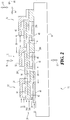
- FIG. 1 that represents an example useful for understanding the invention, some aspects of a non-limiting example of a fuel cell system 10 in accordance with an embodiment of the present invention is schematically depicted.
- FIG. 1 various features, components and interrelationships therebetween of aspects of the present invention are depicted.
- the present embodiment of fuel cell system 10 includes a plurality of electrochemical cells 12, i.e., individual fuel cells, formed on a substrate 14. Electrochemical cells 12 are coupled together in series by interconnects 16. Fuel cell system 10 is a segmented-in-series arrangement deposited on a flat porous ceramic tube, although it will be understood that the present invention is equally applicable to segmented-in-series arrangements on other substrates, such on a circular porous ceramic tube. In various embodiments, fuel cell system 10 may be an integrated planar fuel cell system or a tubular fuel cell system.
- Each electrochemical cell 12 of the present embodiment has an oxidant side 18 and a fuel side 20.
- the oxidant is typically air, but could also be pure oxygen (O 2 ) or other oxidants, e.g., including dilute air for fuel cell systems having air recycle loops, and is supplied to electrochemical cells 12 from oxidant side 18.
- Substrate 14 of the present embodiment is porous, e.g., a porous ceramic material which is stable at fuel cell operation conditions and chemically compatible with other fuel cell materials.
- substrate 14 may be a surface-modified material, e.g., a porous ceramic material having a coating or other surface modification, e.g., configured to prevent or reduce interaction between electrochemical cell 12 layers and substrate 14.
- a fuel such as a reformed hydrocarbon fuel, e.g., synthesis gas
- a fuel is supplied to electrochemical cells 12 from fuel side 20 via channels (not shown) in porous substrate 14.
- a hydrocarbon fuel e.g., synthesis gas
- electrochemical cells using other oxidants and fuels may be employed without departing from the scope of the present invention, e.g., pure hydrogen and pure oxygen.
- fuel is supplied to electrochemical cells 12 via substrate 14 in the present embodiment, it will be understood that in other embodiments of the present invention, the oxidant may be supplied to the electrochemical cells via a porous substrate.
- Fuel cell system 10 can be formed of a plurality of layers screen printed onto substrate 14. Screen printing is a process whereby a woven mesh has openings through which the fuel cell layers are deposited onto substrate 14. The openings of the screen determine the length and width of the printed layers. Screen mesh, wire diameter, ink solids loading and ink rheology determine the thickness of the printed layers. Fuel cell system 10 layers include an anode conductive layer 22, an anode layer 24, an electrolyte layer 26, a cathode layer 28 and a cathode conductive layer 30.
- electrolyte layer 26 is formed of an electrolyte sub-layer 26A and an electrolyte sub-layer 26B. In other embodiments, electrolyte layer 26 may be formed of any number of sub-layers. It will be understood that FIG. 2 is not to scale; for example, vertical dimensions are exaggerated for purposes of clarity of illustration.
- Interconnects for solid oxide fuel cells are preferably electrically conductive in order to transport electrons from one electrochemical cell to another; mechanically and chemically stable under both oxidizing and reducing environments during fuel cell operation; and nonporous, in order to prevent diffusion of the fuel and/or oxidant through the interconnect.
- the interconnect is porous, fuel may diffuse to the oxidant side and burn, resulting in local hot spots that may result in a reduction of fuel cell life, e.g., due to degradation of materials and mechanical failure, as well as reduced efficiency of the fuel cell system.
- the oxidant may diffuse to the fuel side, resulting in burning of the fuel. Severe interconnect leakage may significantly reduce the fuel utilization and performance of the fuel cell, or cause catastrophic failure of fuel cells or stacks.
- fuel cell components may be formed by depositing thin films on a porous ceramic substrate, e.g., substrate 14.
- the films are deposited via a screen printing process, including the interconnect.
- other process may be employed to deposit or otherwise form the thin films onto the substrate.
- the thickness of interconnect layer may be 5 to 30 microns, but can also be much thicker, e.g., 100 microns. If the interconnect is not fully nonporous, e.g., due to sintering porosity, microcracks, voids and other defects introduced during processing, gas or air flux through interconnect layer may be very high, resulting in undesirable effects, as mentioned above. Accordingly, in one aspect of the present invention, the interconnect (interconnect 16) is configured to minimize or eliminate diffusion of the oxidant and fuel therethrough.
- the material of interconnect 16 of the present embodiment is a precious metal, such as Ag, Pd, Au and/or Pt and/or alloys thereof, although other materials may be employed without departing from the scope of the present invention.
- a precious metal such as Ag, Pd, Au and/or Pt and/or alloys thereof
- other materials including precious metal alloys, such as Ag-Pd, Ag-Au, Ag-Pt, Au-Pd, Au-Pt, Pt-Pd, Ag-Au-Pd, Ag-Au-Pt, Ag-Au-Pd-Pt and/or binary, ternary, quaternary alloys in the Pt-Pd-Au-Ag family, inclusive of alloys having minor non-precious metal additions, cermets composed of a precious metal, precious metal alloy, Ni metal and/or Ni alloy and an inert ceramic phase, such as alumina, or ceramic phase with minimum ionic conductivity which will not create significant parasitics, such as YSZ (
- interconnect 16 may be formed of a Ni metal cermet and/or a Ni alloy cermet in addition to or in place of the materials mentioned above.
- the Ni metal cermet and/or the Ni alloy cermet may have one or more ceramic phases, for example and without limitation, a ceramic phase being YSZ (yttria doping is 3-8 mol%, preferably 3-5 mol%), alumina, ScSZ (scandia doping is 4-10 mol%, preferably 4-6 mol%), doped ceria and/or TiO 2 .
- interconnect 16 is y(Pd x Pt 1-x )-(1-y)YSZ.
- x is from 0 to 1 in weight ratio, preferably x is in the range of 0 to 0.5 for lower hydrogen flux.
- Y is from 0.35 to 0.80 in volume ratio, preferably y is in the range of 0.4 to 0.6.
- Anode conductive layer 22 of the present embodiment is an electrode conductive layer formed of a nickel cermet, such as such as Ni-YSZ (yttria doping in zirconia is 3-8 mol%,), Ni-ScSZ (scandia doping is 4-10 mol%, preferably second doping for phase stability for 10 mol% scandia-ZrO 2 ) and/or Ni-doped ceria (such as Gd or Sm doping), doped lanthanum chromite (such as Ca doping on A site and Zn doping on B site), doped strontium titanate (such as La doping on A site and Mn doping on B site) and/or La 1-x Sr x Mn y Cr 1-y O 3 .
- Ni-YSZ yttria doping in zirconia is 3-8 mol%
- Ni-ScSZ scandia doping is 4-10 mol%, preferably second doping for phase stability for 10
- anode conductive layer 22 may be employed such as cermets based in part or whole on precious metal.
- Precious metals in the cermet may include, for example, Pt, Pd, Au, Ag, and/or alloys thereof.
- the ceramic phase may include, for example, an inactive non-electrically conductive phase, including, for example, YSZ, ScSZ and/or one or more other inactive phases, e.g., having desired coefficients of thermal expansion (CTE) in order to control the CTE of the layer to match the CTE of the substrate and electrolyte.
- CTE coefficients of thermal expansion
- the ceramic phase may include Al 2 O 3 and/or a spinel such as NiAl 2 O 4 , MgAl 2 O 4 , MgCr 2 O4, NiCr 2 O 4 .
- the ceramic phase may be electrically conductive, e.g., doped lanthanum chromite, doped strontium titanate and/or one or more forms of LaSrMnCrO..
- anode conductive layer material is 76.5%Pd, 8.5%Ni, 15%3YSZ.
- Anode 24 may be formed of xNiO-(100-x)YSZ (x is from 55 to 75 in weight ratio), yNiO-(100-y)ScSZ (y is from 55 to 75 in weight ratio), NiO-gadolinia stabilized ceria (such as 55wt%NiO-45wt%GDC) and/or NiO samaria stabilized ceria in the present embodiment, although other materials may be employed without departing from the scope of the present invention.
- anode layer 24 may be made of doped strontium titanate, and La 1-x Sr x Mn y Cr 1-y O 3 .(such as La 0.75 Sr 0.25 Mn 0.5 Cr 0.5 O 3 )
- Electrolyte layer 26 of the present embodiment may be made from a ceramic material.
- a proton and/or oxygen ion conducting ceramic may be employed.
- electrolyte layer 26 is formed of YSZ, such as 3YSZ and/or 8YSZ.
- electrolyte layer 26 may be formed of ScSZ, such as 4ScSZ, 6ScSz and/or 10ScSZ in addition to or in place of YSZ. In other embodiments, other materials may be employed.
- electrolyte layer 26 may be made of doped ceria and/or doped lanthanum gallate.
- electrolyte layer 26 is essentially impervious to diffusion therethrough of the fluids used by fuel cell 10, e.g., synthesis gas or pure hydrogen as fuel, as well as, e.g., air or O 2 as an oxidant, but allows diffusion of oxygen ions or protons.
- La 1-x Sr x Co y Fe 1-y O 3 such as La 0.6 Sr 0.4 Co 0.2 Fe 0.8 O 3
- Pr 1-x Sr x MnO 3 such as Pr 0.8 Sr 0.2 MnO 3
- LaNi x Fe 1-x O 3 such as LaNi 0.6 Fe 0.4 O 3
- La 1-x Sr x MnO 3 such as La 0 . 75 Sr 0.25 MnO 3
- Pr 1-x Sr x CoO 3 such as Pr 0.8 Sr 0.2 Co
- cathode conductive layer 30 may be formed of other materials, e.g., a precious metal cermet, although other materials may be employed without departing from the scope of the present invention.
- the precious metals in the precious metal cermet may include, for example, Pt, Pd, Au, Ag and/or alloys thereof.
- the ceramic phase may include, for example, YSZ, ScSZ and Al 2 O 3 , or other ceramic materials.
- cathode conductive layer materials 80wt%Pd-20wt%LSM.
- anode conductive layer 22 is printed directly onto substrate 14, as is a portion of electrolyte sub-layer 26A.
- Anode layer 24 is printed onto anode conductive layer 22.
- Portions of electrolyte layer 26 are printed onto anode layer 24, and portions of electrolyte layer 26 are printed onto anode conductive layer 22 and onto substrate 14.
- Cathode layer 28 is printed on top of electrolyte layer 26.
- Portions of cathode conductive layer 30 are printed onto cathode layer 28 and onto electrolyte layer 26.
- Cathode layer 28 is spaced apart from anode layer 24 in a direction 32 by the local thickness of electrolyte layer 26.
- Anode layer 24 includes anode gaps 34, which extend in a direction 36.
- Cathode layer 28 includes cathode gaps 38, which also extend in direction 36.
- direction 36 is substantially perpendicular to direction 32, although the present invention is not so limited.
- Gaps 34 separate anode layer 24 into a plurality of individual anodes 40, one for each electrochemical cell 12.
- Gaps 38 separate cathode layer 28 into a corresponding plurality of cathodes 42. Each anode 40 and the corresponding cathode 42 that is spaced apart in direction 32 therefrom, in conjunction with the portion of electrolyte layer 26 disposed therebetween, form an electrochemical cell 12.
- anode conductive layer 22 and cathode conductive layer 30 have respective gaps 44 and 46 separating anode conductive layer 22 and cathode conductive layer 30 into a plurality of respective anode conductor films 48 and cathode conductor films 50.
- the terms, "anode conductive layer” and “anode conductor film” may be used interchangeably, in as much as the latter is formed from one or more layers of the former; and the terms, “cathode conductive layer” and “cathode conductor film” may be used interchangeably, in as much as the latter is formed from one or more layers of the former.
- anode conductive layer 22 has a thickness, i.e., as measured in direction 32, of approximately 5-15 microns, although other values may be employed without departing from the scope of the present invention.
- the anode conductive layer may have a thickness in the range of 5-50 microns. In yet other embodiments, different thicknesses may be used, depending upon the particular material and application.
- anode layer 24 has a thickness, i.e., as measured in direction 32, of approximately 5-20 microns, although other values may be employed without departing from the scope of the present invention.
- the anode layer may have a thickness in the range of 5-40 microns. In yet other embodiments, different thicknesses may be used, depending upon the particular anode material and application.
- Electrolyte layer 26, including both electrolyte sub-layer 26A and electrolyte sub-layer 26B, of the present embodiment has a thickness of approximately 5-15 microns with individual sub-layer thicknesses of approximately 5 microns minimum, although other thickness values may be employed without departing from the scope of the present invention.
- the electrolyte layer may have a thickness in the range of 5-40 microns. In yet other embodiments, different thicknesses may be used, depending upon the particular materials and application.
- Cathode layer 28 has a thickness, i.e., as measured in direction 32, of approximately 10-20 microns, although other values may be employed without departing from the scope of the present invention.
- the cathode layer may have a thickness in the range of 10-50 microns. In yet other embodiments, different thicknesses may be used, depending upon the particular cathode material and application.
- Cathode conductive layer 30 has a thickness, i.e., as measured in direction 32, of approximately 5-100 microns, although other values may be employed without departing from the scope of the present invention.
- the cathode conductive layer may have a thickness less than or greater than the range of 5-100 microns.
- different thicknesses may be used, depending upon the particular cathode conductive layer material and application.
- anode conductive layer 22 conducts free electrons away from anode 24 and conducts the electrons to cathode conductive layer 30 via interconnect 16.
- Cathode conductive layer 30 conducts the electrons to cathode 28.
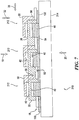
- Interconnect 16 is embedded in electrolyte layer 26, and is electrically coupled to anode conductive layer 22, and extends in direction 32 from anode conductive layer 22 through electrolyte sub-layer 26A toward electrolyte sub-layer 26B, then in direction 36 from one electrochemical cell 12 to the next adjacent electrochemical cell 12, and then in direction 32 again toward cathode conductive layer 30, to which interconnect 16 is electrically coupled.
- interconnect 16 is embedded within an extended portion of electrolyte layer 26, wherein the extended portion of electrolyte layer 26 is a portion of electrolyte layer 26 that extends beyond anode 40 and cathode 42, e.g., in direction 32, and is not sandwiched between anode 40 and cathode 42.
- Interconnect 16 includes a blind primary conductor 52, and two blind auxiliary conductors, or vias 54, 56.
- Blind primary conductor 52 is sandwiched between electrolyte sub-layer 26A and electrolyte sub-layer 26B, and is formed of a body 58 extending between a blind end 60 and a blind end 62 opposite end 60.
- Blind- primary conductor 52 defines a conduction path encased within electrolyte layer 26 and oriented along direction 36, i.e., to conduct a flow of electrons in a direction substantially parallel to direction 36.
- Blind auxiliary conductor 54 has a blind end 64
- blind auxiliary conductor 56 has a blind end 66
- Blind auxiliary conductors 54 and 56 are oriented in direction 32.
- blind relates to the conductor not extending straight through electrolyte layer 26 in the direction of orientation of the conductor, i.e., in the manner of a "blind hole” that ends in a structure, as opposed to a "through hole” that passes through the structure. Rather, the blind ends face portions of electrolyte layer 26.
- end 64 of conductor 54 faces portion 68 electrolyte sub-layer 26B and is not able to "see” through electrolyte sub-layer 26B.
- end 66 of conductor 56 faces portion 70 of electrolyte sub-layer 26A and is not able to "see” through electrolyte sub-layer 26A.
- ends 60 and 62 of body 58 face portions 72 and 74, respectively, and are not able to "see” through electrolyte sub-layer 26A.
- blind primary conductor 52 is a conductive film created with a screen printing process, which is embedded within electrolyte layer 26, sandwiched between electrolyte sub-layers 26A and 26B.
- Anode layer 24 is oriented along a first plane
- cathode layer 28 is oriented along a second plane substantially parallel to the first plane
- electrolyte layer 26 is oriented along a third plane substantially parallel to the first plane
- the conductive film forming blind primary conductor 52 extends in a direction substantially parallel to the first plane.
- the material of blind primary conductor 52 may be a precious metal cermet or an electrically conductive ceramic.
- other materials may be employed in addition to or in place of a precious metal cermet or an electrically conductive ceramic, e.g., a precious metal, such as Ag, Pd, Au and/or Pt, although other materials may be employed without departing from the scope of the present invention.
- precious metal alloys such as Ag-Pd, Ag-Au, Ag-Pt, Au-Pd, Au-Pt, Pt-Pd, Ag-Au-Pd, Ag-Au-Pt, and Ag-Au-Pd-Pt
- cermets composed of precious metal or alloys, Ni metal and/or Ni alloy, and an inert ceramic phase, such as alumina, or ceramic phase with minimum ionic conductivity which will not generate significant parasitic current, such as YSZ, ScSZ, and/or conductive ceramics, such as at least one of LNF (LaNi x Fe 1-x O3), LSM (La 1-x Sr x MnO 3 ), doped strontium titanate, doped yttrium chromites, LSCM (La 1-x Sr x Cr 1-y Mn y O 3 ), and/or other doped lanthanum chromites, and
- LNF LaNi x Fe 1-x O3
- LSM La 1-x S
- blind primary conductor 52 may be formed of a Ni metal cermet and/or a Ni alloy cermet in addition to or in place of the materials mentioned above.
- the Ni metal cermet and/or the Ni alloy cermet may have one or more ceramic phases, for example and without limitation, a ceramic phase being YSZ, alumina, ScSZ, doped ceria and/or TiO 2 .
- blind primary conductor 52 may be formed of materials set forth above with respect to interconnect 16.
- y(Pd x Pt 1-x )-(1-y)YSZ is y(Pd x Pt 1-x )-(1-y)YSZ.
- x is from 0 to 1 in weight ratio.
- x is preferred in the range of 0.5 to 1.
- x is prefered in the range of 0 to 0.5. Because hydrogen has higher flux in Pd.
- Y is from 0.35 to 0.80 in volume ratio, preferably y is in the range of 0.4 to 0.6.
- blind auxiliary conductors 54 and 56 may be formed from the same or different materials than primary conductor 52.
- blind auxiliary conductor 54 is formed during processing of blind primary conductor 52 and from the same material as blind primary conductor 52
- blind auxiliary conductor 56 is formed at the same process step as cathode conductive layer 30 and from the same material as cathode conductive layer 30.
- blind primary conductor 52, blind auxiliary conductor 54 and blind auxiliary conductor 56 may be made from other material combinations without departing from the scope of the present invention.
- blind auxiliary conductor 54 and blind auxiliary conductor 56 may vary with the particular application. For example, with some material combinations, material migration may occur at the interface of interconnect 16 with anode conductive layer 22 and/or cathode conductive layer 30 during either cell fabrication or cell testing, which may cause increased resistance at the interface and higher cell degradation during fuel cell operation. Material may migrate into primary conductor 52 from anode conductive layer 22 and/or cathode conductive layer 30, and/or material may migrate from primary conductor 52 into anode conductive layer 22 and/or cathode conductive layer 30, depending upon the compositions of primary conductor 52, anode conductive layer 22 and cathode conductive layer 30.
- blind auxiliary conductor 54 and blind auxiliary conductor 56 may be formed from a material that yields an electrically conductive chemical barrier layer between primary conductor 52 and a respective one or both of anode conductive layer 22 (anode conductor film 48) and/or cathode conductive layer 30 (cathode conductor film 50).
- This chemical barrier may eliminate or reduce material migration during fuel cell fabrication and operation.
- YSZ yttria doping is 3-5 mol% in zironi
- auxiliary conductor 54 is 50v%(50Pd50Pt)-50v%3YSZ.
- auxiliary conductor 54 is 15%Pd, 19%NiO, 66%NTZ, where NTZ is 73.6wt% NiO, 20.0%TiO 2 , 6.4% 3YSZ.
- auxiliary conductor 56 is 50v%(50Pd50Pt)-50v%3YSZ.
- auxiliary conductor 56 is 15%Pd, 19%NiO, 66%NTZ, where NTZ is 73.6wt% NiO, 20.0%TiO 2 , 6.4% 3YSZ.
- auxiliary conductor 54 has a width 76, i.e., in direction 36, of approximately 0.4 mm, although greater or lesser widths may be used without departing from the scope of the present invention.
- auxiliary conductor 56 has a width 78, i.e., in direction 36, of approximately 0.4 mm, although greater or lesser widths may be used without departing from the scope of the present invention.
- Primary conductor 52 has a length in direction 36 that defines a minimum diffusion distance 80 for any hydrogen that may diffuse through interconnect 16, e.g., due to sintering porosity, microcracks, voids and/or other defects introduced into interconnect 16 during processing.
- the diffusion distance 80 is 0.6 mm, although greater or lesser widths may be used without departing from the scope of the present invention.
- the film thickness 82 of primary conductor 52, i.e., as measured in direction 32, is approximately 5-15 microns.
- the total height 84 of interconnect 16 in direction 32 is approximately 10-25 microns, which generally corresponds to the thickness of electrolyte layer 26.
- the total diffusion distance for hydrogen diffusing through interconnect 16 may include the height of auxiliary conductor 54 and auxiliary conductor 56 in direction 32, which may be given by subtracting from the total height 84 the film thickness 82 of primary conductor 52, which yields approximately 10 microns.
- the diffusion distance is predominantly controlled by diffusion distance 80, e.g., since the heights of auxiliary conductors 54 and 56 represent only a small fraction of the total diffusion distance.
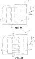
- FIGS. 4A and 4B that represent useful examples for understanding the invention, a plan view of a continuous "strip" configuration of interconnect 16 and a plan view of a "via” configuration of interconnect 16 are respectively depicted.
- the term, "strip,” pertains to the configuration being in the form of a single long conductor that is comparatively narrow in width as compared to length.
- the primary conductor takes the form of a continuous strip 52A extending in a direction 86 that in the present embodiment is substantially perpendicular to both directions 32 and 36, and runs approximately the length in direction 86 of electrochemical cell 12.
- direction 32 extends into and out of the plane of the drawing, and hence is represented by an "X" within a circle.
- the term, "via,” pertains to a relatively small conductive pathway through a material that connects electrical components.
- the primary conductor takes the form of a plurality of vias 52B, e.g., each having a width in direction 86 of only approximately 0.4 mm, although greater or lesser widths may be used without departing from the scope of the present invention.
- the minimum diffusion area of interconnect 16 is controlled by the diffusion area of primary conductor 52, which serves as a diffusion flow orifice that restricts the diffusion of fluid.
- primary conductor 52 serves as a diffusion flow orifice that restricts the diffusion of fluid.
- fluid e.g., oxidant and fuel in liquid and/or gaseous form may diffuse through interconnect 16.
- Such diffusion is controlled, in part, by the film thickness 82.
- the diffusion area is given by the width of continuous strip 52A in direction 86 times the film thickness 82, whereas in the "via” configuration, the diffusion area is given by the width of each via 52B in direction 86 times the film thickness 82 times the number of vias 52B.
- interconnect 88 transfers electrical power from an anode conductor 92 to a cathode conductor 94.
- the length 96 of interconnect 88 in direction 32 which corresponds to the thickness of electrolyte layer 90, is assumed to be the 10-15 microns, e.g., similar to interconnect 16, and the width of interconnect 88, e.g., the width of the open slot in the electrolyte 96 into which interconnect 88 is printed, in direction 36 is assumed to be the minimum printable via dimension 98 in direction 36 with current industry technology, which is approximately 0.25 mm.
- the length of interconnect 88 in direction 86 is assumed to be 0.4 mm.
- the diffusion flow area for one via is approximately 0.25 mm times 0.4 mm, which equals 0.1 mm 2 .
- the limiting dimension is the minimum 0.25 mm screen printed via dimension 98.
- the diffusion flow area of the interconnect may be reduced, thereby potentially decreasing diffusion of oxidant and/or fuel through the interconnector, e.g., in the event the interconnect is not fully non-porous (such as, for example, due to process limitations and/or manufacturing defects), or the interconnect is a mixed ion and electronic conductor.
- the diffusion distance in interconnect 88 corresponds to the thickness 96 of interconnect 88, which in the depicted example is also the thickness of electrolyte layer 90, i.e., 10-15 microns.
- the diffusion distance of the inventive blind primary connector 52 is diffusion distance 80, which is 0.6 mm, and which is 40-60 times the diffusion distance of interconnect 88 (0.6 mm divided by 10-15 microns), which is many times the thickness of the electrolyte.
- the diffusion distance of the interconnect may be substantially increased, thereby potentially decreasing diffusion of oxidant and/or fuel through the interconnector.
- the flow of fuel and/or air through an interconnect made from a given material and microstructure depends on the flow area and flow distance.
- Some embodiments of the present invention may reduce fuel and/or air flow through the interconnect by 10 2 to 10 4 magnitude, e.g., if the connector is not non-porous, depending on the specific dimension of the interconnect used.
- processing-related defects such as sintering porosity, microcracks and voids are typically from sub-microns to a few microns in size (voids) or a few microns to 10 microns (microcracks).
- voids voids
- microcracks 10 microns
- the presence of a defect may provide a direct flowpath through the interconnect, or at least decrease the diffusion distance by a substantial percentage.
- voids voids
- microcracks a few microns to 10 microns
- microcracks With a diffusion distance of only 10-15 microns, the presence of a defect may provide a direct flowpath through the interconnect, or at least decrease the diffusion distance by a substantial percentage.
- a design diffusion distance of 10 microns In the presence of a 10 micron defect, a direct flowpath for the flow of hydrogen and/or oxidant would occur, since such a defect would open a direct pathway through the interconnect (it is noted that the anode/conductive layer
- a 10 micron defect in the inventive interconnect 16 would have only negligible effect on the 0.6 mm design diffusion distance of primary conductor 52, i.e., reducing the 0.6 mm design diffusion distance to 0.59 mm, which is a relatively inconsequential reduction caused by the presence of the defect.
- FIGS. 6A and 6B that represent examples useful for understanding the invention, some aspects of a non-limiting example of an interconnect having a blind primary conductor in the form of a via 52C extending in direction 86 are depicted.
- direction 32 extends into and out of the plane of the drawing, and hence is represented by an "X" within a circle.
- direction 36 extends into and out of the plane of the drawing, and hence is represented by an "X" within a circle.
- Via 52C is similar to via 52B, except that it extends in direction 86 rather than direction 36, for example, as indicated by diffusion distance 80 being oriented in direction 86.
- FIGS. 6A and 6B exemplarily depict only a single via 52C, embodiments of the present invention may include a plurality of such vias extending along direction 86.
- FIGS. 6A and 6B The direction of electron flow in FIGS. 6A and 6B is illustrated by three dimensional flowpath line 100. Electrons flow in direction 36 through anode conductor film 48 toward auxiliary conductor 54, and then flow in direction 32 through auxiliary conductor 54 toward via 52C. The electrons then flow in direction 86 through via 52C toward auxiliary conductor 56, and then flow in direction 32 through auxiliary conductor 56 into cathode conductor film 50, after which the electrons flow in direction 36 through cathode conductor film 50, e.g., to the next electrochemical cell.
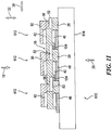
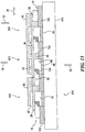
- Fuel cell system 210 includes a plurality of electrochemical cells 212 disposed on a substrate 214, each electrochemical cell 212 having a seal in the form of a ceramic seal 102. Fuel cell system 210 also includes the components set forth above and described with respect to fuel cell system 10, e.g., including interconnects 16 having blind primary conductors 52 and blind auxiliary conductors or vias 54 and 56; an oxidant side 18; a fuel side 20; electrolyte layers 26; anodes 40; cathodes 42, anode conductor films 48 and cathode conductor films 50.
- auxiliary conductor 56 of interconnect 16 is formed of the same material as cathode conductor film 50, whereas auxiliary conductor 54 of interconnect 16 is formed of the same material as anode conductor film 48.
- Blind primary conductor 52 of interconnect 16 is formed of the same material described above with respect to interconnect 16 in the embodiment of FIG. 2 .
- auxiliary conductor 54 and/or auxiliary conductor 56 may be formed of the same material as blind primary conductor 52, or may be formed of different materials.
- blind primary conductor 52 is in the form of a continuous strip, e.g., continuous strip 52A depicted in FIG. 4A .
- blind primary conductor 52 is in the form of a plurality of vias, such as vias 52B in FIG. 4B .
- blind primary conductor 52 may take other forms not explicitly set forth herein.
- ceramic seal 102 is applied onto porous substrate 214, and is positioned horizontally (in the perspective of FIG. 7 ) between the anode conductor film 48 of one electrochemical cell 212 and the auxiliary conductor 54 of the adjacent electrochemical cell 212. In other embodiments, ceramic seal 102 may be located in other orientations and locations. Ceramic seal 102 has a thickness, i.e., as measured in direction 32, of approximately 5-30 microns, although other thickness values may be employed in other embodiments. In one form, ceramic seal 102 is impervious to gases and liquids, such as the fuel and oxidants employed by electrochemical cells 212, and is configured to prevent the leakage of gases and liquids from substrate 214 in those areas where it is applied.
- ceramic seal 102 may be substantially impervious to gases and liquids, and may be configured to reduce leakage of gases and liquids from substrate 214 in those areas where it is applied, e.g., relative to other configurations that do not employ a ceramic seal. Ceramic seal 102 is configured to provide an essentially "gas-tight" seal between substrate 214 and fuel cell components disposed on the side of ceramic seal 102 opposite of that of substrate 214.
- ceramic seal 102 is positioned to prevent or reduce leakage of gases and liquids from substrate 214 into interconnect 16.
- ceramic seal 102 extends in direction 36, and is positioned vertically (in direction 32) between porous substrate 214 on the bottom and blind primary conductor 52 of interconnect 16 and electrolyte 26 on the top, thereby preventing the leakages of gases and liquids into the portions of blind primary conductor 52 (and electrolyte 26) that are overlapped by ceramic seal 102.
- ceramic seal 102 may be disposed in other suitable locations in addition to or in place of that illustrated in FIG. 7 .
- Blind primary conductor 52 is embedded between a portion of ceramic seal 102 on the bottom and a portion of extended electrolyte 26 on the top.
- the diffusion distance in the embodiment of FIG. 7 is primarily defined by the length of the overlap of interconnect 16 by both ceramic seal 102 and electrolyte 26 in direction 36. In one form, the overlap is 0.3-0.6 mm, although in other embodiments, other values may be employed. Interconnect 16 extends into the active electrochemical cell 212 area. In some embodiments, the primary interconnect area of the configuration illustrated in FIG. 7 may be smaller than other designs, which may increase the total active cell area on substrate 214, which may increase the efficiency of fuel cell system 210.
- Ceramic seal 102 is formed from a ceramic material.
- the ceramic material used to form ceramic seal 102 is yittria stabilized zirconia, such as 3YSZ.
- the material used to form ceramic seal 102 is scandia stabilized zirconia, such as 4ScSZ.
- the material used to form ceramic seal 102 is alumina.
- the material used to form ceramic seal 102 is nonconductive pyrochlore materials, such as La 2 Zr 2 O 7 .
- inventions may employ other ceramics, e.g., depending upon various factors, such as compatibility with the materials of adjacent portions of each electrochemical cell 212 and substrate 214, the fuels and oxidants employed by fuel cell system 210, and the local transient and steady-state operating temperatures of fuel cell system 210. Still other embodiments may employ materials other than ceramics.
- Fuel cell system 310 includes a plurality of electrochemical cells 312 disposed on a substrate 314, each electrochemical cell 312 including a ceramic seal 102. Fuel cell system 310 also includes the components set forth above and described with respect to fuel cell system 10, e.g., including interconnects 16 having blind primary conductors 52 and blind auxiliary conductors or vias 54 and 56; an oxidant side 18; a fuel side 20; electrolyte layers 26; anodes 40; cathodes 42, anode conductor films 48 and cathode conductor films 50. The description of substrate 14 applies equally to substrate 314.
- interconnect 16 is formed predominantly by the material of anode conductor film 48, and hence, blind primary conductor 52 and auxiliary conductor 54 in the embodiment of FIG. 8 may be considered as extensions of anode conductor film 48.
- blind primary conductor 52 and auxiliary conductor 54 are depicted as being formed by the material of anode conductor film 48, whereas auxiliary conductor 56 is formed of the materials set forth above for interconnect 16 in the embodiment of FIG. 2 .
- blind primary conductor 52 is in the form of a continuous strip, e.g., continuous strip 52A depicted in FIG. 4A .
- blind primary conductor 52 is in the form of a plurality of vias, such as vias 52B in FIG. 4B .
- blind primary conductor 52 may take other forms not explicitly set forth herein.
- Ceramic seal 102 is positioned to prevent or reduce leakage of gases and liquids from substrate 314 into interconnect 16.
- ceramic seal 102 is positioned vertically (in direction 32) between porous substrate 314 on the bottom and blind primary conductor 52 and electrolyte 26 on the top, thereby preventing the leakages of gases and liquids into the portions of blind primary conductor 52 that are overlapped by ceramic seal 102.
- Blind primary conductor 52 is embedded between a portion of ceramic seal 102 on the bottom and extended electrolyte 26 on the top.
- the diffusion distance in the embodiment of FIG. 8 is primarily defined by the length of the overlap of interconnect 16 by both ceramic seal 102 and electrolyte 26 in direction 36.
- the overlap is 0.3-0.6 mm, although in other embodiments, other values may be employed.
- interconnect 16 does not need to be as dense (in order to prevent or reduce leakage) as other designs that do not include a seal, such as ceramic seal 102.
- interconnect 16 may be formed of the materials used to form anode conductor layer 48 and/or cathode conductor layer 50.
- FIG. 9 that represents an example useful for understanding the invention, an embodiment is depicted wherein interconnect 16 is formed entirely of the materials used to form anode conductor layer 48 and cathode conductor layer 50.
- FIG. 9 schematically depicts some aspects of a non-limiting example of a fuel cell system 410.
- Fuel cell system 410 includes a plurality of electrochemical cells 412 disposed on a substrate 414, each electrochemical cell 412 including a ceramic seal 102. Fuel cell system 410 also includes the components set forth above and described with respect to fuel cell system 10, e.g., including interconnects 16 having blind primary conductors 52 and blind auxiliary conductors or vias 54 and 56; an oxidant side 18; a fuel side 20; electrolyte layers 26; anodes 40; cathodes 42, anode conductor films 48 and cathode conductor films 50. The description of substrate 14 applies equally to substrate 414. In the embodiment of FIG.
- blind primary conductor 52 and auxiliary conductor 54 are formed of the same material used to form anode conductor film 48, and are formed in the same process steps used to form anode conductor film 48. Hence, blind primary conductor 52 and auxiliary conductor 54 in the embodiment of FIG. 9 may be considered as extensions of anode conductor film 48.
- auxiliary conductor 56 is formed of the same material used to form cathode conductor film 50, and is formed in the same process steps used to form cathode conductor film 50. Hence, auxiliary conductor 56 in the embodiment of FIG. 9 may be considered as an extension of cathode conductor film 50.
- some embodiments of the present invention include an electrically conductive chemical barrier (e.g., as discussed above, and/or chemical barrier 104, discussed below with respect to FIGS. 10-15 ) to prevent or reduce such material diffusion.
- an electrically conductive chemical barrier e.g., as discussed above, and/or chemical barrier 104, discussed below with respect to FIGS. 10-15
- chemical barrier 104 may be configured to prevent or reduce material migration or diffusion at the interface between the interconnect and an anode, and and/or between the interconnect and an anode conductor film, and/or between the interconnect and a cathode, and and/or between the interconnect and a cathode conductor film which may improve the long term durability of the interconnect.
- material migration may take place at the interface between an interconnect formed of a precious metal cermet, and an anode conductor film and/or anode formed of a Ni-based cermet.
- the material migration may take place in both directions, e.g., Ni migrating from the anode conductive layer/conductor film and/or anode into the interconnect, and precious metal migrating from the interconnect into the conductive layer/conductor film and/or anode.
- the material migration may result in increased porosity at or near the interface between the interconnect and the anode conductor film and/or anode, and may result in the enrichment of one or more non or low-electronic conducting phases at the interface, yielding a higher area specific resistance (ASR), and hence resulting in reduced fuel cell performance.
- ASR area specific resistance
- Material migration between the interconnect and the cathode and/or between the interconnect and the cathode conductor film may also or alternatively result in deleterious effects on fuel cell performance.
- some embodiments employ a chemical barrier, e.g., chemical barrier 104, that is configured to prevent or reduce material migration or diffusion at the interface between the interconnect and an adjacent electrically conductive component, such as one or more of an anode, an anode conductive layer/conductor film, a cathode and/or a cathode conductive layer/conductor film, and hence prevent or reduce material migration (diffusion) that might otherwise result in deleterious effect, e.g., the formation of porosity and the enrichment of one or more non or low-electronic conducting phases at the interface.
- Chemical barrier 104 may be formed of one or both of two classes of materials; cermet and/or conductive ceramic.
- the ceramic phase may be one or more of an inert filler; a ceramic with low ionic conductivity, such as YSZ; and an electronic conductor.
- chemical barrier 104 may be formed of one or more materials, including, without limitation, Ni cermet or Ni-precious metal cermet.
- the precious metal phase may be, for example and without limitation, one or more of Ag, Au, Pd, Pt, or one or more alloys of Ag, Au, Pd and/or Pt.
- chemical barrier 104 may be formed of one or more materials, including, without limitation precious metal cermet.
- the precious metal phase may be, for example and without limitation, one or more of Ag, Au, Pd, Pt, or one or more alloys of Ag, Au, Pd and/or Pt.
- M RE one or more rare earth cations, for example and without limitation
- LSCF La 0.6 Sr 0.4 Co 0.2 Fe 0.8 O 3
- the selection of the specific material(s) for chemical barrier 104 may vary with the needs of the application, e.g., depending upon cost, ease of manufacturing, the type of materials used for the component(s) electrically adjacent to interconnect 16 and/or one of its subcomponents, e.g., blind primary conductor 52, auxiliary conductor 54 and auxiliary conductor 56.
- anode side chemical barrier materials is 15%Pd, 19%NiO, 66%NTZ, where NTZ is 73.6wt% NiO, 20.0%TiO 2 , 6.4% YSZ.
- anode side chemical barrier materials is doped ceria, such as Gd 0.1 Ce 0.9 O 2 .
- an interconnect formed of 50v%(96Pd6Au)-50v%YSZ cermet directly interfacing with an anode conductive layer formed of 20wt%Pd-Ni-spinel showed significant degradation in about 10 hours of testing, and fuel cell failure at about 25 hours of testing resulting from material migration between the interconnect and the anode conductive layer.
- ASR for the interconnect showed no degradation after approximately 8000 hours of testing, and instead showed slight improvement, yielding final values of .05 ohm-cm 2 and .06 ohm-cm 2 in the two test articles.
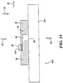
- Fuel cell system 510 includes a chemical barrier 104. Fuel cell system 510 also includes some the components set forth above and described with respect to fuel cell system 10, e.g., including an interconnects 16 having a blind primary conductor 52; an oxidant side 18; a fuel side 20; electrolyte layers 26; anodes 40; and cathodes 42.
- fuel cell system 510 may include a plurality of each such components, e.g., arranged in series in direction 36, e.g., similar to embodiments described above.
- the description of substrate 14 applies equally to substrate 514.
- chemical barrier 104 is disposed between anode 40 and interconnect 16 (blind primary conductor 52), extending in direction 32 between anode 40 and interconnect 16, and is configured to prevent material migration between anode 40 and interconnect 16 (blind primary conductor 52).
- Chemical barrier 104 may be formed from one or more of the materials set forth above with respect to the embodiments of FIGS. 10-15 .
- Fuel cell system 610 includes a plurality of electrochemical cells 612 disposed on a substrate 614, each electrochemical cell 612 including a chemical barrier 104. Fuel cell system 610 also includes the components set forth above and described with respect to fuel cell system 10, e.g., including interconnects 16 having blind primary conductors 52 and blind auxiliary conductors or vias 54 and 56; an oxidant side 18; a fuel side 20; electrolyte layers 26; anodes 40; cathodes 42, anode conductor films 48 and cathode conductor films 50.
- chemical barrier 104 is disposed between anode conductor film 48 and interconnect 16 (blind primary conductor 52), extending in direction 32 between anode conductor film 48 and interconnect 16, and is configured to prevent material migration between anode conductor film 48 and interconnect 16 (blind primary conductor 52).
- Chemical barrier 104 may be formed from one or more of the materials set forth above with respect to the embodiments of FIGS. 10-15 .
- a portion of electrolyte layer 26 is disposed between anode 40 and chemical barrier 104, extending in direction 36 between anode 40 and chemical barrier 104.
- Fuel cell system 710 includes a plurality of electrochemical cells 712 disposed on a substrate 714, each electrochemical cell 712 including a ceramic seal 102 and a chemical barrier 104. Fuel cell system 710 also includes the components set forth above and described with respect to fuel cell system 10, e.g., including interconnects 16 having blind primary conductors 52 and blind auxiliary conductors or vias 54 and 56; an oxidant side 18; a fuel side 20; electrolyte layers 26; anodes 40; cathodes 42, anode conductor films 48 and cathode conductor films 50.
- ceramic seal 102 is positioned to prevent or reduce leakage of gases and liquids from substrate 714 into interconnect 16 (blind interconnect 52), and extends in direction 36 between the anode conductor film 48 of one electrochemical cell 712 and the auxiliary conductor 54 of an adjacent electrochemical cell 712.
- ceramic seal 102 is positioned vertically (in direction 32) between porous substrate 714 on the bottom and blind primary conductor 52 of interconnect 16 and electrolyte 26 on the top, thereby preventing the leakages of gases and liquids from substrate 714 into the portions of blind primary conductor 52 (and electrolyte 26) that are overlapped by ceramic seal 102.
- ceramic seal 102 may be disposed in other suitable locations in addition to or in place of that illustrated in FIG. 12 .
- Ceramic seal 102 may be formed of one or more of the materials set forth above with respect to the embodiment of FIG. 7 .
- a portion of blind primary conductor 52 is embedded between ceramic seal 102 on the bottom and electrolyte 26 on the top.
- the diffusion distance in the embodiment of FIG. 12 is primarily defined by the length of the overlap of blind primary conductor 52 by both ceramic seal 102 and electrolyte 26 in direction 36.
- chemical barrier 104 is disposed between anode conductor film 48 and interconnect 16 (blind primary conductor 52), extending in direction 32 between anode conductor film 48 and both blind primary conductor 52 and auxiliary conductor 54 of interconnect 16, and is configured to prevent material migration between anode conductor film 48 and blind primary conductor 52 and auxiliary conductor 54.
- Chemical barrier 104 may be formed from one or more of the materials set forth above with respect to the examples illustrated in FIGS. 10-15 .
- Fuel cell system 810 includes a plurality of electrochemical cells 812 disposed on a substrate 814, each electrochemical cell 812 including a ceramic seal 102 and a chemical barrier 104. Fuel cell system 810 also includes the components set forth above and described with respect to fuel cell system 10, e.g., including interconnects 16 having blind primary conductors 52 and auxiliary conductors or vias 54 and 56; an oxidant side 18; a fuel side 20; electrolyte layers 26; anodes 40; cathodes 42, anode conductor films 48 and cathode conductor films 50.
- the description of substrate 14 applies equally to substrate 814.
- ceramic seal 102 is positioned to prevent or reduce leakage of gases and liquids from substrate 814 into interconnect 16 (blind interconnect 52), and extends in direction 36 between the anode 40 and anode conductor film 48 of one electrochemical cell 812 and the anode 40 and anode conductor film 48 of an adjacent electrochemical cell 812.
- ceramic seal 102 is positioned vertically (in direction 32) between porous substrate 814 on the bottom and blind primary conductor 52 of interconnect 16 and electrolyte 26 on the top, thereby preventing the leakages of gases and liquids from substrate 714 into the portions of blind primary conductor 52 (and electrolyte 26) that are overlapped by ceramic seal 102.
- ceramic seal 102 may be disposed in other suitable locations in addition to or in place of that illustrated in FIG. 13 .
- Ceramic seal 102 may be formed of one or more of the materials set forth above with respect to the embodiment of FIG. 7 .
- a portion of blind primary conductor 52 is embedded between ceramic seal 102 on the bottom, and electrolyte 26 on the top.
- the diffusion distance in the embodiment of FIG. 13 is primarily defined by the length of the overlap of blind primary conductor 52 by both ceramic seal 102 and electrolyte 26 in direction 36.
- chemical barrier 104 is disposed between anode 40 and blind primary conductor 52, and is configured to prevent material migration between anode 40 and blind primary conductor 52.
- chemical barrier 104 also functions as auxiliary conductor 54.
- auxiliary conductor 54 may be formed separately from chemical barrier 104.
- Chemical barrier 104 may be formed from one or more of the materials set forth above with respect to the embodiments of FIGS. 10-15 .
- Fuel cell system 910 includes a chemical barrier 104. Fuel cell system 910 also includes some the components set forth above and described with respect to fuel cell system 10, e.g., including an interconnects 16 having a blind primary conductor 52; an oxidant side 18; a fuel side 20; electrolyte layers 26; anodes 40; and cathodes 42.
- fuel cell system 910 may include a plurality of each such components, e.g., arranged in series in direction 36, e.g., similar to embodiments described above.
- the description of substrate 14 applies equally to substrate 914.
- chemical barrier 104 is disposed between cathode 42 and interconnect 16 (blind primary conductor 52), extending in direction 32 between cathode 42 and interconnect 16, and is configured to prevent material migration between cathode 42 and interconnect 16 (blind primary conductor 52).
- Chemical barrier 104 may be formed from one or more of the materials set forth above with respect to the embodiments of FIGS. 10-15 .
- Fuel cell system 1010 includes a plurality of electrochemical cells 612 disposed on a substrate 1014, each electrochemical cell 1012 including a chemical barrier 104. Fuel cell system 1010 also includes the components set forth above and described with respect to fuel cell system 10, e.g., including interconnects 16 having blind primary conductors 52 and blind auxiliary conductors or vias 54 and 56; an oxidant side 18; a fuel side 20; electrolyte layers 26; anodes 40; cathodes 42, anode conductor films 48 and cathode conductor films 50.
- chemical barrier 104 is disposed between cathode conductor film 50 and interconnect 16 (blind primary conductor 52), extending in direction 32 between cathode conductor film 50 and interconnect 16 (blind primary conductor 52), and is configured to prevent material migration between cathode conductor film 50 and interconnect 16 (blind primary conductor 52).
- Chemical barrier 104 may be formed from one or more of the materials set forth above with respect to the embodiments of FIGS. 10-15 . In the embodiment of FIG. 15 , chemical barrier 104 also functions as auxiliary conductor 56.
- the inventors have determined that in some fuel cells, under some operating conditions, the cathode conductive layer/conductor film, the electrolyte, and portions of the interconnect, e.g., vias, can form parasitic cells within or between each electrochemical cell, particularly where there is overlap between the cathode conductive layer/conductor film and the electrolyte.
- the cathode conductive layer/conductor film functions as a cathode
- the interconnect e.g., vias formed of precious metal cermet
- the parasitic cells consume fuel during fuel cell operation, thereby reducing the efficiency of the fuel cell system.
- the steam generated by the parasitic cells may create local high oxygen partial pressure that may result in the oxidation of Ni that may have diffused into precious metal phase of the interconnect (e.g., via) materials, resulting in degradation of the interconnect.
- the inventors performed tests that confirmed the existence of parasitic cells. The tests confirmed that, although significant degradation did not occur at some temperatures, e.g., 900°C, under the testing times, degradation of the interconnect occurred at higher operating temperatures, e.g., 925°C after approximately 700 hours of testing. Post test analysis showed Ni migration from the anode conductive layer/conductor film side to the cathode conductive layer/conductor film side of the interconnect through the precious metal phase in blind primary conductor 52, which was accelerated by the higher operating temperature.
- a high oxygen partial pressure resulting from steam formed by the parasitic cells caused Ni oxidation at the interface of extended electrolyte 26 and blind primary interconnect 52 near the boundary between the cathode conductive layer/conductor film and the electrolyte, which segregated from the precious metal of the interconnect. Continued NiO accumulation at the interface between the blind primary conductor 52 and the electrolyte 26, and continued Ni migration would likely result in failure of the interconnect.
- the inventors employed a separation feature (gap 106 of FIGS. 16 and 17 ; and insulator 108 of FIGS. 18 and 19 ) between the cathode conductive layer/conductor film and the electrolyte to separate, i.e., space apart, the cathode conductive layer/conductor film and the electrolyte from contacting each other, thus eliminating the parasitic cells.
- some embodiments of the present invention include a separation feature, e.g., gap 106, between the cathode conductive layer/conductor film and the electrolyte, which prevents the establishment of parasitic cells.
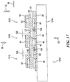
- Fuel cell system 1110 includes a plurality of electrochemical cells 1112 disposed on a substrate 1114, each electrochemical cell 1112 including a ceramic seal 102, a chemical barrier 104, and a separation feature in the form of gap 106.
- Fuel cell system 1110 also includes the components set forth above and described with respect to fuel cell system 10, e.g., including interconnects 16 having blind primary conductors 52 and blind auxiliary conductors or vias 54 and 56; an oxidant side 18; a fuel side 20; electrolyte layers 26; anodes 40; cathodes 42, anode conductor films 48 and cathode conductor films 50.
- the description of substrate 14 applies equally to substrate 1114.
- Gap 106 extends in direction 36 between cathode conductor film 50 (e.g., formed of one or more cathode conductive layers 30) and electrolyte layer 26.
- ceramic seal 102 is positioned to prevent or reduce leakage of gases and liquids from substrate 1114 into interconnect 16 (blind primary conductor 52), and extends in direction 36 between the anode conductor film 48 of one electrochemical cell 1112 and the auxiliary conductor 54 of an adjacent electrochemical cell 1112.
- ceramic seal 102 is positioned vertically (in direction 32) between porous substrate 1114 on the bottom and blind primary conductor 52 of interconnect 16 and electrolyte 26 on the top, thereby preventing the leakages of gases and liquids from substrate 1114 into the portions of blind primary conductor 52 (and electrolyte 26) that are overlapped by ceramic seal 102.
- ceramic seal 102 may be disposed in other suitable locations in addition to or in place of that illustrated in FIG. 12 .
- Ceramic seal 102 may be formed of one or more of the materials set forth above with respect to FIG. 7 .
- a portion of blind primary conductor 52 is embedded between ceramic seal 102 on the bottom, and extended electrolyte 26 on the top. The diffusion distance in the embodiment of FIG. 16 is primarily defined by the length of the overlap of blind primary conductor 52 by both ceramic seal 102 and electrolyte 26 in direction 36.
- chemical barrier 104 is disposed between anode conductor film 48 and interconnect 16 (blind primary conductor 52), extending in direction 32 between anode conductor film 48 and both blind primary conductor 52 and auxiliary conductor 54 of interconnect 16, and is configured to prevent material migration between anode conductor film 48 and blind primary conductor 52 and auxiliary conductor 54.
- Chemical barrier 104 may be formed from one or more of the materials set forth above with respect to FIGS. 10-15 .
- gap 106 is configured to prevent formation of a parasitic fuel cell between cathode conductor film 50, electrolyte layer 26 and blind primary conductor 52.
- gap 106 in the embodiment of FIG. 16 is employed in conjunction with a fuel cell system having ceramic seal 102, chemical barrier 104 and anode conductor film 48, in other embodiments, gap 106 may be employed in fuel cell systems that do not include components corresponding to one or more of ceramic seal 102, chemical barrier 104 and anode conductor film 48.
- Fuel cell system 1210 includes a plurality of electrochemical cells 1212 disposed on a substrate 1214, each electrochemical cell 1212 including a chemical barrier 104 and a separation feature in the form of gap 106.
- Fuel cell system 1210 also includes the components set forth above and described with respect to fuel cell system 10, e.g., including interconnects 16 having blind primary conductors 52 and blind auxiliary conductors or vias 54 and 56; an oxidant side 18; a fuel side 20; electrolyte layers 26; anodes 40; cathodes 42, anode conductor films 48 and cathode conductor films 50.
- the description of substrate 14 applies equally to substrate 1214.
- chemical barrier 104 is disposed between anode conductor film 48 and interconnect 16 (blind primary conductor 52), extending in direction 32 between anode conductor film 48 and interconnect 16, and is configured to prevent material migration between anode conductor film 48 and interconnect 16 (blind primary conductor 52).
- Chemical barrier 104 may be formed from one or more of the materials set forth above with respect to FIGS. 10-15 .
- a portion of electrolyte layer 26 is disposed between anode 40 and chemical barrier 104, extending in direction 36 between anode 40 and chemical barrier 104.
- gap 106 is configured to prevent formation of a parasitic fuel cell between auxiliary conductor 56 (formed of the same material as cathode conductor film 50), electrolyte layer 26 and blind primary conductor 52.
- gap 106 in the embodiment of FIG. 17 is employed in conjunction with a fuel cell system having chemical barrier 104 and anode conductor film 48, in other embodiments, gap 106 may be employed in fuel cell systems that do not include components corresponding to one or more of chemical barrier 104 and anode conductor film 48.
- Fuel cell system 1310 includes a plurality of electrochemical cells 1312 disposed on a substrate 1314, each electrochemical cell 1312 including a ceramic seal 102, a chemical barrier 104, and a separation feature in the form of an insulator 108.
- Fuel cell system 1310 also includes the components set forth above and described with respect to fuel cell system 10, e.g., including interconnects 16 having blind primary conductors 52 and blind auxiliary conductors or vias 54 and 56; an oxidant side 18; a fuel side 20; electrolyte layers 26; anodes 40; cathodes 42, anode conductor films 48 and cathode conductor films 50.
- the description of substrate 14 applies equally to substrate 1314.
- Insulator 108 extends in direction 36 between cathode conductor film 50 (e.g., formed of one or more cathode conductive layers 30) and electrolyte layer 26.
- ceramic seal 102 is positioned to prevent or reduce leakage of gases and liquids from substrate 1314 into interconnect 16 (blind primary conductor 52), and extends in direction 36 between the anode conductor film 48 of one electrochemical cell 1312 and the auxiliary conductor 54 of an adjacent electrochemical cell 1312.
- ceramic seal 102 is positioned vertically (in direction 32) between porous substrate 1314 on the bottom and blind primary conductor 52 of interconnect 16 and electrolyte 26 on the top, thereby preventing the leakages of gases and liquids from substrate 1314 into the portions of blind primary conductor 52 (and electrolyte 26) that are overlapped by ceramic seal 102.
- ceramic seal 102 may be disposed in other suitable locations in addition to or in place of that illustrated in FIG. 12 .
- Ceramic seal 102 may be formed of one or more of the materials set forth above with respect to FIG. 7 .
- a portion of blind primary conductor 52 is embedded between ceramic seal 102 on the bottom, and extended electrolyte 26 on the top.
- the diffusion distance in the embodiment of FIG. 18 is primarily defined by the length of the overlap of blind primary conductor 52 by both ceramic seal 102 and electrolyte 26 in direction 36.
- chemical barrier 104 is disposed between anode conductor film 48 and interconnect 16 (blind primary conductor 52), extending in direction 32 between anode conductor film 48 and both blind primary conductor 52 and auxiliary conductor 54 of interconnect 16, and is configured to prevent material migration between anode conductor film 48 and blind primary conductor 52 and auxiliary conductor 54.
- Chemical barrier 104 may be formed from one or more of the materials set forth above with respect to the embodiments of FIGS. 10-15 .
- insulator 108 is configured to prevent formation of a parasitic fuel cell between cathode conductor film 50, electrolyte layer 26 and blind primary conductor 52.
- insulator 108 is formed from an insulating nonconductive materials, such as aluminum oxide (Al 2 O 3 ), pyrochlore, such as In other embodiments, La 2 Zr 2 O 7 , Pr 2 Zr 2 O 7 , and SrZrO 3 .other materials may be employed to form insulator 108, e.g., one or more other types of non-conducting ceramics in addition to or in place of aluminum oxide.
- Al 2 O 3 aluminum oxide
- pyrochlore such as La 2 Zr 2 O 7 , Pr 2 Zr 2 O 7 , and SrZrO 3 .
- other materials may be employed to form insulator 108, e.g., one or more other types of non-conducting ceramics in addition to or in place of aluminum oxide.
- insulator 108 may be employed in fuel cell systems that do not include components corresponding to one or more of ceramic seal 102, chemical barrier 104 and anode conductor film 48.
- Fuel cell system 1410 includes a plurality of electrochemical cells 1412 disposed on a substrate 1414, each electrochemical cell 1412 including a chemical barrier 104 and a separation feature in the form of insulator 108.
- Fuel cell system 1410 also includes the components set forth above and described with respect to fuel cell system 10, e.g., including interconnects 16 having blind primary conductors 52 and blind auxiliary conductors or vias 54 and 56; an oxidant side 18; a fuel side 20; electrolyte layers 26; anodes 40; cathodes 42, anode conductor films 48 and cathode conductor films 50.
- the description of substrate 14 applies equally to substrate 1414.
- chemical barrier 104 is disposed between anode conductor film 48 and interconnect 16 (blind primary conductor 52), extending in direction 32 between anode conductor film 48 and interconnect 16, and is configured to prevent material migration between anode conductor film 48 and interconnect 16 (blind primary conductor 52).
- Chemical barrier 104 may be formed from one or more of the materials set forth above with respect to the embodiments of FIGS. 10-15 .
- a portion of electrolyte layer 26 is disposed between anode 40 and chemical barrier 104, extending in direction 36 between anode 40 and chemical barrier 104.
- insulator 108 is configured to prevent formation of a parasitic fuel cell between auxiliary conductor 56 (formed of the same material as cathode conductor film 50), electrolyte layer 26 and blind primary conductor 52.
- Insulator 108 may be formed of the materials set forth above in the embodiment of FIG. 18 .
- insulator 108 in the embodiment of FIG. 19 is employed in conjunction with a fuel cell system having chemical barrier 104 and anode conductor film 48, in other embodiments, insulator 108 may be employed in fuel cell systems that do not include components corresponding to one or more of chemical barrier 104 and anode conductor film 48.
- FIGS. 16-19 various features, components and interrelationships therebetween of aspects of embodiments of the present invention are depicted.
- the present invention is not limited to the particular embodiments of FIGS. 16-19 and the components, features and interrelationships therebetween as are illustrated in FIGS. 16-19 and described herein.
- parasitic cells may be undesirably formed.
- the embodiments discussed above with respect to FIGS. 16-19 provide certain approaches to resolving the parasitic cell problem.
- the inventors have also created other approaches to solving the parasitic cell problem, based on material selection, e.g., the material from which the interconnect and/or vias (e.g., interconnect 16, including blind primary conductor 52, auxiliary conductor 54 and/or auxiliary conductor 56, and/or other interconnect and/or via configurations not mentioned herein) are formed.
- precious metal- La 2 Zr 2 O 7 pyrochlore cermet may be employed for primary interconnect material for segmented-in-series fuel cell, or via material for multi-layer ceramic interconnect.
- La 2 Zr 2 O 7 pyrochlore could fully replace doped zirconia, or partially replace doped zirconia to keep ionic phase below its percolation to eliminate or reduce ionic conduction.
- the composition of the interconnect and/or via(s), e.g., one or more of the previously mentioned compositions for the interconnect and/or via(s), is altered to include non-ionic conducting ceramic phases in the composition of the interconnect and/or via(s).
- the interconnect and/or via may be formed, all or in part, of a cermet, such as those previously described with respect to interconnect 16, including blind primary conductor 52, auxiliary conductor 54 and/or auxiliary conductor 56, but also or alternatively including one or more non-ionic conductive ceramic phases.
- a cermet such as those previously described with respect to interconnect 16, including blind primary conductor 52, auxiliary conductor 54 and/or auxiliary conductor 56, but also or alternatively including one or more non-ionic conductive ceramic phases.
- examples include, without limitation, SrZrO 3 , La 2 Zr 2 O 7 pyrochlore, Pr 2 Zr 2 O 7 pyrochlore, BaZrO 3 , MgAl 2 O 4 spinel, NiAl 2 O 4 spinel, MgCr 2 O 4 spinel, NiCr 2 O 4 spinel, Y 3 Al 5 O 12 and other garnets with various A- and B-site substitution, and alumina.
- non-ionic conductive ceramic phases are also contemplated herein in addition to or in place of the examples set forth herein.
- materials may include the coefficient of thermal expansion of the ceramic phase(s), e.g., relative to the coefficient thermal expansion of the porous substrate.
- preferred materials for chemical compatibility with adjacent fuel cell layers may include precious metal-pyrochlore cermets, wherein the general class of pyrochlores is (M RE ) 2 Zr 2 O 7 , wherein M RE is a rare earth cation, for example and without limtiation La, Pr, Nd, Gd, Sm, Ho, Er, and/or Yb.
- nonionic phases such as SrZrO 3 , MgAl 2 O 4 spinel, NiAl 2 O 4 spinel, alumina and pyrochlore compositions partially or completely replace the ionic conducting YSZ, e.g., of previously described interconnects and/or vias.
- pyrochlore powders and/or one or more of the other nonionic phases replace YSZ sufficiently to render the balance of the YSZ to be below a percolation threshold to eliminate ionic conductivity across the interconnect/via.
- the YSZ volume fraction of the via is purposely reduced to less than 30v% to minimize any ionic conductivity within the via material.
- the composition of the interconnect and/or via(s), e.g., one or more of the previously mentioned compositions for the interconnect and/or via(s), is altered to include a reactant phase to form non-ionic conducting ceramic phases during firing of the fuel cell, e.g., by the inclusion of rare earth oxides in the compound used to form the interconnect/via(s).
- all or portions interconnect 16 or other interconnects or vias may include a reactant phase in the form of rare earth oxide, e.g., within the screen printing ink, at less than the stoichiometric ratio to form pyrochlore being one mole of the oxides of La, Pr, Nd, Gd, Sm, Ho, Er, Yb to two moles of the zirconia content of the via.
- the minimum rare earth oxide required is about 13mole% ceramic composition in order to reduce YSZ phase below 30v% percolation. In other embodiments, other rare earth oxide amounts may be employed.
- the zirconia phase may still be able to exist at greater than the percolation threshold, since the insulating pyrochlore phase could form along grain boundaries.
- SrZrO 3 nonionic phases could be created in-situ through addition of SrO powder as a reactant phase, e.g., to the interconnect inks, at less than the stoichimetric ratio of 1 mole SrO to 1 mole ZrO 2 .
- all or portions interconnect 16 or other interconnects or vias may include a content of rare earth oxide, e.g., within the screen printing ink, at greater than the stoichiometric ratio of pyrochlore being one mole of the oxides, e.g., of La, Pr, Nd, Gd, Sm, Ho, Er, and/or Yb, to two moles of the zirconia content of the via in the overall cermet composition (e.g., cermet compositions for all or part of interconnect 16 set forth herein) which reacts with the YSZ during firing of the fuel cell to form pyrochlore within the interconnect/via, and the unreacted rare earth oxide will further react with the extended electrolyte in the vicinity of the interconnect during electrolyte firing to form a pyrochlore film on the electrolyte surface, e.g., on the surface of electrolyte 26, which will sufficiently disrupt the pathways for oxygen ionic conductivity.
- the rare earth oxide amount is from 33mole% to 50mole% based on the total ceramic phase. In other embodiments, other rare earth oxide amounts may be employed.
- the excess rare earth oxide may ensure the absence of ionic conductivity. However, too much excess rare earth remaining within the interconnect/via could cause the via to be susceptible to moisture induced damage on phase change to the rare earth hydroxides. Hence, it is desirable in some embodiments to limit the amount of rare earth oxides to less than 10% over the stoichiometric ratio.
- SrZrO 3 nonionic phases could be created in-situ within the via and adjacent extended electrolyte through addition of SrO powder to the interconnect inks in excess of the stoichimetric ratio of 1 mole SrO to 1 mole ZrO 2 .
- a lower limit is approximately 15-20 mole% SrO based on the ceramic phase, in order to form SrZrO3 to reduce YSZ below the percolation threshold.
- other lower limits may apply.
- an upper limit is about 50-60 mole% SrO based on the ceramic phase (SrO + Zr02). In other embodiments, other upper limits may apply.
- interconnect 16 or other interconnects or vias may include a content of rare earth oxide at the stoichiometric ratio with YSZ to lead to full reactivity to (M RE ) 2 Zr 2 O 7.
- Firing temperatures for using a reactant phase to form the non-ionic conducting ceramic phases during firing of the fuel cell may vary with the needs of the particular application. Considerations include, for example and without limitation, the sinterability of different materials, powder particle size, specific surface area. Other material and/or processing parameters may also affect the selected firing temperature. For example, If the temperature is too low, the electrolyte may have higher porosity and cause leakage. If the temperature is too high, it may cause other issues, such as too high an anode density, which may reduce electrochemical activity, or may cause substrate dimensional changes, etc. Hence, the actual firing temperature for purposes of using one or more reactant phases to form one or more non-ionic conducting ceramic phases may vary as between applications.
- the method may include preparing a screen printable ink that incorporates the rare earth oxide, YSZ and the precious metal; printing the interconnect/via(s); drying the ink; firing the printed interconnect/via(s) at the desired temperature, e.g., at a temperature or within a temperature range set forth above; and holding the composition at the firing temperature for a desired period, e.g., in the range of 1-5 hours.
- non-ionic conducting phases or reactant phases may be employed to minimize the ionic conductivity of the interconnect.
- Tables 1-8 provide compositional information for some aspects of non-limiting experimental fuel cell and fuel cell component examples produced in accordance with some aspects of some embodiments of the present invention. It will be understood the present invention is in no way limited to the examples provided below.
- the columns entitled “General Composition” illustrate some potential compositional ranges, including some preferred ranges, for some materials described herein, whereas, the columns entitled “Specific Composition” illustrates the materials used in the test articles/materials.
- Embodiments of the present invention include a fuel cell system, comprising a plurality of electrochemical cells, each electrochemical cell formed of an anode, a cathode spaced apart from the anode, and an electrolyte disposed between the anode and the cathode; an interconnect electrically coupling a pair of electrically adjacent electrochemical cells, the interconnect electrically coupling the anode of one electrochemical cell to the cathode of the other electrochemical cell; an electrode conductive layer electrically coupled to the interconnect; and a separation feature configured to space apart the electrode conductive layer from the electrolyte layer.
- the electrode conductive layer is a cathode conductive layer electrically coupled to the cathode and to the interconnect.
- the interconnect includes a portion embedded within the electrolyte.
- the separation feature is configured to prevent the formation of a parasitic cell formed of the electrode conductive layer, the electrolyte layer and the interconnect.
- the electrode conductive layer is a cathode conductive layer.
- the separation feature is a gap between the electrode conductive layer and the electrolyte layer.
- the separation feature is an insulator disposed between the electrode conductive layer and the electrolyte layer.
- the insulator is formed of non-insulating materials.
- the insulator is aluminum oxide (Al 2 O 3 ).
- the insulator is pyrochlore.
- the insulator is at least one of La 2 Zr 2 O 7 , Pr 2 Zr 2 O 7 , and SrZrO 3 .
- Embodiments of the present invention include a fuel cell system, comprising: a cathode of a first electrochemical cell; an electrolyte; an anode of a second electrochemical cell spaced apart from the cathode by the electrolyte; a cathode conductive layer adjoining the cathode; an interconnect configured to conduct free electrons between the anode and the cathode, wherein the interconnect adjoins both the cathode conductive layer and the electrolyte; and a separation feature configured to separate the electrode conductive layer from the electrolyte layer.
- the interconnect includes a portion embedded within the electrolyte.
- the separation feature is configured to prevent the formation of a parasitic cell formed of the cathode conductive layer, the electrolyte and the interconnect.
- the separation feature is a gap between the electrode conductive layer and the electrolyte layer.
- the separation feature is an insulator disposed between the electrode conductive layer and the electrolyte layer.
- the insulator is formed of non-insulating materials.
- the insulator is aluminum oxide (Al2O3).
- the insulator is pyrochlore.
- the insulator is at least one of La2Zr207, Pr2Zr2O7, and SrZrO3.
Description
- The present invention generally relates to fuel cells and, in particular, to an interconnect for a fuel cell.
- Fuel cells, fuel cell systems and interconnects for fuel cells and fuel cell systems remain an area of interest. Some existing systems have various shortcomings, drawbacks, and disadvantages relative to certain applications. Accordingly, there remains a need for further contributions in this area of technology.
-
U.S. Patent Publication No. 2011/033779 discloses insulating compositions for use in solid oxide fuel cells. Such compositions can be used to prevent seal damage and increase the electrical and ion efficiency. - The present invention includes a fuel cell system having an interconnect that reduces or eliminates diffusion (leakage) of fuel and oxidant by providing an increased diffusion distance and reduced diffusion flow area.
- The description herein makes reference to the accompanying drawings wherein like reference numerals refer to like parts throughout the several views, and wherein:
-
FIG. 1 schematically depicts some aspects of a non-limiting example of a fuel cell system. -
FIG. 2 schematically depicts some aspects of a non-limiting example of a cross section of a fuel cell system. -
FIG. 3 is an enlarged cross sectional view of a portion of the interconnect ofFIG. 2 . -
FIGS. 4A and 4B depict some alternate embodiments of interconnect configurations. -
FIG. 5 depicts a contrasting hypothetical interconnect. -
FIGS. 6A and 6B show a top view and a side view, respectively, of some aspects of a non-limiting example of an interconnect. -
FIG. 7 schematically depicts some aspects of a non-limiting example of a cross section of a fuel cell system having a ceramic seal. -
FIG. 8 schematically depicts some aspects of a non-limiting example of a cross section of a fuel cell system having a ceramic seal. -
FIG. 9 schematically depicts some aspects of a non-limiting example of a cross section of a fuel cell system having a ceramic seal. -
FIG. 10 schematically depicts some aspects of a non-limiting example of a cross section of a fuel cell system having a chemical barrier. -
FIG. 11 schematically depicts some aspects of a non-limiting example of a cross section of t a fuel cell system having a chemical barrier. -
FIG. 12 schematically depicts some aspects of a non-limiting example of a cross section of a fuel cell system having a chemical barrier and a ceramic seal. -
FIG. 13 schematically depicts some aspects of a non-limiting example of a cross section of a fuel cell system having a chemical barrier and a ceramic seal. -
FIG. 14 schematically depicts some aspects of a non-limiting example of a cross section of a fuel cell system having a chemical barrier. -
FIG. 15 schematically depicts some aspects of a non-limiting example of a cross section of a fuel cell system having a chemical barrier. -
FIG. 16 schematically depicts some aspects of a non-limiting example of a cross section of an embodiment of the present invention having a chemical barrier, a ceramic seal, and a gap between a cathode conductor film and an electrolyte layer. -
FIG. 17 schematically depicts some aspects of a non-limiting example of a cross section of an embodiment of the present invention having a chemical barrier, a ceramic seal, and a gap between an interconnect auxiliary conductor and an electrolyte layer. -
FIG. 18 schematically depicts some aspects of a non-limiting example of a cross section of an embodiment of the present invention having a chemical barrier, a ceramic seal, and an insulator between a cathode conductor film and an electrolyte layer. -
FIG. 19 schematically depicts some aspects of a non-limiting example of a cross section of an embodiment of the present invention having a chemical barrier, a ceramic seal, and an insulator between an interconnect auxiliary conductor and an electrolyte layer. - For purposes of promoting an understanding of the principles of the invention, reference will now be made to the embodiments illustrated in the drawings, and specific language will be used to describe the same. It will nonetheless be understood that no limitation of the scope of the invention is intended by the illustration and description of certain embodiments of the invention. In addition, any alterations and/or modifications of the illustrated and/or described embodiment(s) are contemplated as being within the scope of the present invention. Further, any other applications of the principles of the invention, as illustrated and/or described herein, as would normally occur to one skilled in the art to which the invention pertains, are contemplated as being within the scope of the present invention.
- Referring to the drawings, and in particular
FIG. 1 , that represents an example useful for understanding the invention, some aspects of a non-limiting example of afuel cell system 10 in accordance with an embodiment of the present invention is schematically depicted. InFIG. 1 , various features, components and interrelationships therebetween of aspects of the present invention are depicted. - The present embodiment of
fuel cell system 10 includes a plurality ofelectrochemical cells 12, i.e., individual fuel cells, formed on asubstrate 14.Electrochemical cells 12 are coupled together in series byinterconnects 16.Fuel cell system 10 is a segmented-in-series arrangement deposited on a flat porous ceramic tube, although it will be understood that the present invention is equally applicable to segmented-in-series arrangements on other substrates, such on a circular porous ceramic tube. In various embodiments,fuel cell system 10 may be an integrated planar fuel cell system or a tubular fuel cell system. - Each
electrochemical cell 12 of the present embodiment has anoxidant side 18 and afuel side 20. The oxidant is typically air, but could also be pure oxygen (O2) or other oxidants, e.g., including dilute air for fuel cell systems having air recycle loops, and is supplied toelectrochemical cells 12 fromoxidant side 18.Substrate 14 of the present embodiment is porous, e.g., a porous ceramic material which is stable at fuel cell operation conditions and chemically compatible with other fuel cell materials. In other embodiments,substrate 14 may be a surface-modified material, e.g., a porous ceramic material having a coating or other surface modification, e.g., configured to prevent or reduce interaction betweenelectrochemical cell 12 layers andsubstrate 14. A fuel, such as a reformed hydrocarbon fuel, e.g., synthesis gas, is supplied toelectrochemical cells 12 fromfuel side 20 via channels (not shown) inporous substrate 14. Although air and synthesis gas reformed from a hydrocarbon fuel are employed in the present embodiment, it will be understood that electrochemical cells using other oxidants and fuels may be employed without departing from the scope of the present invention, e.g., pure hydrogen and pure oxygen. In addition, although fuel is supplied toelectrochemical cells 12 viasubstrate 14 in the present embodiment, it will be understood that in other embodiments of the present invention, the oxidant may be supplied to the electrochemical cells via a porous substrate. - Referring to
FIG. 2 , that represents an example useful for understanding the invention, some aspects of a non-limiting example offuel cell system 10 are described in greater detail.Fuel cell system 10 can be formed of a plurality of layers screen printed ontosubstrate 14. Screen printing is a process whereby a woven mesh has openings through which the fuel cell layers are deposited ontosubstrate 14. The openings of the screen determine the length and width of the printed layers. Screen mesh, wire diameter, ink solids loading and ink rheology determine the thickness of the printed layers.Fuel cell system 10 layers include an anodeconductive layer 22, ananode layer 24, anelectrolyte layer 26, acathode layer 28 and a cathodeconductive layer 30. In one form,electrolyte layer 26 is formed of anelectrolyte sub-layer 26A and anelectrolyte sub-layer 26B. In other embodiments,electrolyte layer 26 may be formed of any number of sub-layers. It will be understood thatFIG. 2 is not to scale; for example, vertical dimensions are exaggerated for purposes of clarity of illustration. - Interconnects for solid oxide fuel cells (SOFC) are preferably electrically conductive in order to transport electrons from one electrochemical cell to another; mechanically and chemically stable under both oxidizing and reducing environments during fuel cell operation; and nonporous, in order to prevent diffusion of the fuel and/or oxidant through the interconnect. If the interconnect is porous, fuel may diffuse to the oxidant side and burn, resulting in local hot spots that may result in a reduction of fuel cell life, e.g., due to degradation of materials and mechanical failure, as well as reduced efficiency of the fuel cell system. Similarly, the oxidant may diffuse to the fuel side, resulting in burning of the fuel. Severe interconnect leakage may significantly reduce the fuel utilization and performance of the fuel cell, or cause catastrophic failure of fuel cells or stacks.
- For segmented-in-series cells, fuel cell components may be formed by depositing thin films on a porous ceramic substrate, e.g.,
substrate 14. In one form, the films are deposited via a screen printing process, including the interconnect. In other embodiments, other process may be employed to deposit or otherwise form the thin films onto the substrate. The thickness of interconnect layer may be 5 to 30 microns, but can also be much thicker, e.g., 100 microns. If the interconnect is not fully nonporous, e.g., due to sintering porosity, microcracks, voids and other defects introduced during processing, gas or air flux through interconnect layer may be very high, resulting in undesirable effects, as mentioned above. Accordingly, in one aspect of the present invention, the interconnect (interconnect 16) is configured to minimize or eliminate diffusion of the oxidant and fuel therethrough. - The material of
interconnect 16 of the present embodiment is a precious metal, such as Ag, Pd, Au and/or Pt and/or alloys thereof, although other materials may be employed without departing from the scope of the present invention. For example, in other embodiments, it is alternatively contemplated that other materials may be employed, including precious metal alloys, such as Ag-Pd, Ag-Au, Ag-Pt, Au-Pd, Au-Pt, Pt-Pd, Ag-Au-Pd, Ag-Au-Pt, Ag-Au-Pd-Pt and/or binary, ternary, quaternary alloys in the Pt-Pd-Au-Ag family, inclusive of alloys having minor non-precious metal additions, cermets composed of a precious metal, precious metal alloy, Ni metal and/or Ni alloy and an inert ceramic phase, such as alumina, or ceramic phase with minimum ionic conductivity which will not create significant parasitics, such as YSZ (yttria stabilized zirconia, also known as yttria doped zirconia, yttria doping is 3-8 mol%, preferably 3-5 mol%), ScSZ (scandia stabilized zirconia, scandia doping is 4-10 mol%, preferably 4-6 mol%), and/or conductive ceramics, such as conductive perovskites with A or B-site substitutions or doping to achieve adequate phase stability and/or sufficient conductivity as an interconnect, e.g., including at least one of LNF (LaNixFe1-xO3, preferably x=0.6), LSM (La1-xSrxMnO3, x=0.1 to 0.3), doped ceria, doped strontium titanate (such as LaxSr1-xTiO3-δ, x=0.1 to 0.3), LSCM (La1-xSrxCr1-yMnyO3, x=0.1 to 0.3 and y=0.25 to 0.75), doped yttrium chromites (such as Y1-xCaxCrO3-δ, x=0.1-0.3) and/or other doped lanthanum chromites (such as La1-xCaxCrO3-δ, x=0.15-0.3), and conductive ceramics, such as at least one of LNF (LaNixFe1-xO3, preferably x=0.6), LSM (La1-xSrxMnO3, x=0.1 to 0.3), doped strontium titanate, doped yttrium chromites, LSCM (La1-xSrxCr1-yMnyO3), and other doped lanthanum chromites. In some embodiments, it is contemplated that all or part ofinterconnect 16 may be formed of a Ni metal cermet and/or a Ni alloy cermet in addition to or in place of the materials mentioned above. The Ni metal cermet and/or the Ni alloy cermet may have one or more ceramic phases, for example and without limitation, a ceramic phase being YSZ (yttria doping is 3-8 mol%, preferably 3-5 mol%), alumina, ScSZ (scandia doping is 4-10 mol%, preferably 4-6 mol%), doped ceria and/or TiO2. - One example of materials for
interconnect 16 is y(PdxPt1-x)-(1-y)YSZ. Where x is from 0 to 1 in weight ratio, preferably x is in the range of 0 to 0.5 for lower hydrogen flux. Y is from 0.35 to 0.80 in volume ratio, preferably y is in the range of 0.4 to 0.6. - Anode
conductive layer 22 of the present embodiment is an electrode conductive layer formed of a nickel cermet, such as such as Ni-YSZ (yttria doping in zirconia is 3-8 mol%,), Ni-ScSZ (scandia doping is 4-10 mol%, preferably second doping for phase stability for 10 mol% scandia-ZrO2) and/or Ni-doped ceria (such as Gd or Sm doping), doped lanthanum chromite (such as Ca doping on A site and Zn doping on B site), doped strontium titanate (such as La doping on A site and Mn doping on B site) and/or La1-xSrxMnyCr1-yO3. Alternatively, it is considered that other materials for anodeconductive layer 22 may be employed such as cermets based in part or whole on precious metal. Precious metals in the cermet may include, for example, Pt, Pd, Au, Ag, and/or alloys thereof. The ceramic phase may include, for example, an inactive non-electrically conductive phase, including, for example, YSZ, ScSZ and/or one or more other inactive phases, e.g., having desired coefficients of thermal expansion (CTE) in order to control the CTE of the layer to match the CTE of the substrate and electrolyte. In some embodiments, the ceramic phase may include Al2O3 and/or a spinel such as NiAl2O4, MgAl2O4, MgCr2O4, NiCr2O4. In other embodiments, the ceramic phase may be electrically conductive, e.g., doped lanthanum chromite, doped strontium titanate and/or one or more forms of LaSrMnCrO.. - One example of anode conductive layer material is 76.5%Pd, 8.5%Ni, 15%3YSZ.
-
Anode 24 may be formed of xNiO-(100-x)YSZ (x is from 55 to 75 in weight ratio), yNiO-(100-y)ScSZ (y is from 55 to 75 in weight ratio), NiO-gadolinia stabilized ceria (such as 55wt%NiO-45wt%GDC) and/or NiO samaria stabilized ceria in the present embodiment, although other materials may be employed without departing from the scope of the present invention. For example, it is alternatively considered thatanode layer 24 may be made of doped strontium titanate, and La1-xSrxMnyCr1-yO3.(such as La0.75Sr0.25Mn0.5Cr0.5O3) -
Electrolyte layer 26 of the present embodiment, e.g., electrolyte sub-layer 26A and/orelectrolyte sub-layer 26B, may be made from a ceramic material. In one form, a proton and/or oxygen ion conducting ceramic, may be employed. In one form,electrolyte layer 26 is formed of YSZ, such as 3YSZ and/or 8YSZ. In other embodiments,electrolyte layer 26 may be formed of ScSZ, such as 4ScSZ, 6ScSz and/or 10ScSZ in addition to or in place of YSZ. In other embodiments, other materials may be employed. For example, it is alternatively considered thatelectrolyte layer 26 may be made of doped ceria and/or doped lanthanum gallate. In any event,electrolyte layer 26 is essentially impervious to diffusion therethrough of the fluids used byfuel cell 10, e.g., synthesis gas or pure hydrogen as fuel, as well as, e.g., air or O2 as an oxidant, but allows diffusion of oxygen ions or protons. -
Cathode layer 28 may be formed at least one of of LSM (La1-xSrxMnO3,x=0.1 to 0.3), La1-xSrxFeO3,(such as x=0.3), La1-xSrxCoyFe1-yO3 (such as La0.6Sr0.4Co0.2Fe0.8O3) and/or Pr1-xSrxMnO3 (such as Pr0.8Sr0.2MnO3), although other materials may be employed without departing from the scope of the present invention. For example, it is alternatively considered that Ruddlesden-Popper nickelates and La1-xCaxMnO3 (such as La0.8Ca0.2MnO3) materials may be employed. - Cathode
conductive layer 30 is an electrode conductive layer formed of a conductive ceramic, for example, at least one of LaNixFe1-xO3 (such as LaNi0.6Fe0.4O3), La1-xSrxMnO3 (such as La0.75Sr0.25MnO3), doped lanthanum chromites (such as La1-xCaxCrO3-δ, x=0.15-0.3), and/or Pr1-xSrxCoO3, such as Pr0.8Sr0.2CoO3. In other embodiments,cathode conductive layer 30 may be formed of other materials, e.g., a precious metal cermet, although other materials may be employed without departing from the scope of the present invention. The precious metals in the precious metal cermet may include, for example, Pt, Pd, Au, Ag and/or alloys thereof. The ceramic phase may include, for example, YSZ, ScSZ and Al2O3, or other ceramic materials. - One example of cathode conductive layer materials is 80wt%Pd-20wt%LSM.
- In
FIG. 2 , anodeconductive layer 22 is printed directly ontosubstrate 14, as is a portion ofelectrolyte sub-layer 26A.Anode layer 24 is printed onto anodeconductive layer 22. Portions ofelectrolyte layer 26 are printed ontoanode layer 24, and portions ofelectrolyte layer 26 are printed onto anodeconductive layer 22 and ontosubstrate 14.Cathode layer 28 is printed on top ofelectrolyte layer 26. Portions ofcathode conductive layer 30 are printed ontocathode layer 28 and ontoelectrolyte layer 26.Cathode layer 28 is spaced apart fromanode layer 24 in adirection 32 by the local thickness ofelectrolyte layer 26. -
Anode layer 24 includesanode gaps 34, which extend in adirection 36.Cathode layer 28 includescathode gaps 38, which also extend indirection 36. In the present embodiment,direction 36 is substantially perpendicular todirection 32, although the present invention is not so limited.Gaps 34separate anode layer 24 into a plurality ofindividual anodes 40, one for eachelectrochemical cell 12.Gaps 38separate cathode layer 28 into a corresponding plurality ofcathodes 42. Eachanode 40 and the correspondingcathode 42 that is spaced apart indirection 32 therefrom, in conjunction with the portion ofelectrolyte layer 26 disposed therebetween, form anelectrochemical cell 12. - Similarly, anode
conductive layer 22 andcathode conductive layer 30 haverespective gaps 44 and 46 separating anodeconductive layer 22 andcathode conductive layer 30 into a plurality of respectiveanode conductor films 48 andcathode conductor films 50. The terms, "anode conductive layer" and "anode conductor film" may be used interchangeably, in as much as the latter is formed from one or more layers of the former; and the terms, "cathode conductive layer" and "cathode conductor film" may be used interchangeably, in as much as the latter is formed from one or more layers of the former. - In
FIG. 2 , anodeconductive layer 22 has a thickness, i.e., as measured indirection 32, of approximately 5-15 microns, although other values may be employed without departing from the scope of the present invention. For example, it is considered that in other embodiments, the anode conductive layer may have a thickness in the range of 5-50 microns. In yet other embodiments, different thicknesses may be used, depending upon the particular material and application. - Similarly,
anode layer 24 has a thickness, i.e., as measured indirection 32, of approximately 5-20 microns, although other values may be employed without departing from the scope of the present invention. For example, it is considered that in other embodiments, the anode layer may have a thickness in the range of 5-40 microns. In yet other embodiments, different thicknesses may be used, depending upon the particular anode material and application. -
Electrolyte layer 26, including bothelectrolyte sub-layer 26A andelectrolyte sub-layer 26B, of the present embodiment has a thickness of approximately 5-15 microns with individual sub-layer thicknesses of approximately 5 microns minimum, although other thickness values may be employed without departing from the scope of the present invention. For example, it is considered that in other embodiments, the electrolyte layer may have a thickness in the range of 5-40 microns. In yet other embodiments, different thicknesses may be used, depending upon the particular materials and application. -
Cathode layer 28 has a thickness, i.e., as measured indirection 32, of approximately 10-20 microns, although other values may be employed without departing from the scope of the present invention. For example, it is considered that in other embodiments, the cathode layer may have a thickness in the range of 10-50 microns. In yet other embodiments, different thicknesses may be used, depending upon the particular cathode material and application. - Cathode
conductive layer 30 has a thickness, i.e., as measured indirection 32, of approximately 5-100 microns, although other values may be employed without departing from the scope of the present invention. For example, it is considered that in other embodiments, the cathode conductive layer may have a thickness less than or greater than the range of 5-100 microns. In yet other embodiments, different thicknesses may be used, depending upon the particular cathode conductive layer material and application. - In each
electrochemical cell 12, anodeconductive layer 22 conducts free electrons away fromanode 24 and conducts the electrons tocathode conductive layer 30 viainterconnect 16. Cathodeconductive layer 30 conducts the electrons tocathode 28. -
Interconnect 16 is embedded inelectrolyte layer 26, and is electrically coupled to anodeconductive layer 22, and extends indirection 32 from anodeconductive layer 22 throughelectrolyte sub-layer 26A towardelectrolyte sub-layer 26B, then indirection 36 from oneelectrochemical cell 12 to the next adjacentelectrochemical cell 12, and then indirection 32 again towardcathode conductive layer 30, to whichinterconnect 16 is electrically coupled. In particular, at least a portion ofinterconnect 16 is embedded within an extended portion ofelectrolyte layer 26, wherein the extended portion ofelectrolyte layer 26 is a portion ofelectrolyte layer 26 that extends beyondanode 40 andcathode 42, e.g., indirection 32, and is not sandwiched betweenanode 40 andcathode 42. - Referring to
FIG. 3 , that represents an example useful for understanding the invention, some aspects of a non-limiting example ofinterconnect 16 are described in greater detail.Interconnect 16 includes a blindprimary conductor 52, and two blind auxiliary conductors, orvias primary conductor 52 is sandwiched betweenelectrolyte sub-layer 26A andelectrolyte sub-layer 26B, and is formed of abody 58 extending between ablind end 60 and ablind end 62opposite end 60. Blind-primary conductor 52 defines a conduction path encased withinelectrolyte layer 26 and oriented alongdirection 36, i.e., to conduct a flow of electrons in a direction substantially parallel todirection 36. Blindauxiliary conductor 54 has ablind end 64, and blindauxiliary conductor 56 has ablind end 66. Blindauxiliary conductors direction 32. As that term is used herein, "blind" relates to the conductor not extending straight throughelectrolyte layer 26 in the direction of orientation of the conductor, i.e., in the manner of a "blind hole" that ends in a structure, as opposed to a "through hole" that passes through the structure. Rather, the blind ends face portions ofelectrolyte layer 26. For example, end 64 ofconductor 54 facesportion 68electrolyte sub-layer 26B and is not able to "see" throughelectrolyte sub-layer 26B. Similarly, end 66 ofconductor 56 facesportion 70 ofelectrolyte sub-layer 26A and is not able to "see" throughelectrolyte sub-layer 26A. Likewise, ends 60 and 62 ofbody 58face portions electrolyte sub-layer 26A. - In
FIG. 3 , blindprimary conductor 52 is a conductive film created with a screen printing process, which is embedded withinelectrolyte layer 26, sandwiched betweenelectrolyte sub-layers Anode layer 24 is oriented along a first plane,cathode layer 28 is oriented along a second plane substantially parallel to the first plane,electrolyte layer 26 is oriented along a third plane substantially parallel to the first plane, and the conductive film forming blindprimary conductor 52 extends in a direction substantially parallel to the first plane. - In one form, the material of blind
primary conductor 52 may be a precious metal cermet or an electrically conductive ceramic. In other embodiments, other materials may be employed in addition to or in place of a precious metal cermet or an electrically conductive ceramic, e.g., a precious metal, such as Ag, Pd, Au and/or Pt, although other materials may be employed without departing from the scope of the present invention. In various embodiments, it is contemplated that one or more of many materials may be employed, including precious metal alloys, such as Ag-Pd, Ag-Au, Ag-Pt, Au-Pd, Au-Pt, Pt-Pd, Ag-Au-Pd, Ag-Au-Pt, and Ag-Au-Pd-Pt, cermets composed of precious metal or alloys, Ni metal and/or Ni alloy, and an inert ceramic phase, such as alumina, or ceramic phase with minimum ionic conductivity which will not generate significant parasitic current, such as YSZ, ScSZ, and/or conductive ceramics, such as at least one of LNF (LaNixFe1-xO3), LSM (La1-xSrxMnO3), doped strontium titanate, doped yttrium chromites, LSCM (La1-xSrxCr1-yMnyO3), and/or other doped lanthanum chromites, and conductive ceramics, such as LNF (LaNixFe1-xO3), for example, LaNi0.6Fe0.4O3, LSM (La1-xSrxMnO3), such as La0.75Sr0.25MnO3, doped strontium titanate, doped yttrium chromites, LSCM (La1-xSrxCr1-yMnyO3), such as La0.75Sr0.25Cr0.5Mn0.5O3, and other doped lanthanum chromites. In other embodiments, it is contemplated that blindprimary conductor 52 may be formed of a Ni metal cermet and/or a Ni alloy cermet in addition to or in place of the materials mentioned above. The Ni metal cermet and/or the Ni alloy cermet may have one or more ceramic phases, for example and without limitation, a ceramic phase being YSZ, alumina, ScSZ, doped ceria and/or TiO2. In various embodiments, blindprimary conductor 52 may be formed of materials set forth above with respect tointerconnect 16. - One example of materials for blind
primary conductor 52 is y(PdxPt1-x)-(1-y)YSZ. Where x is from 0 to 1 in weight ratio. For cost reduction, x is preferred in the range of 0.5 to 1. For better performance and higher system efficiency, x is prefered in the range of 0 to 0.5. Because hydrogen has higher flux in Pd. Y is from 0.35 to 0.80 in volume ratio, preferably y is in the range of 0.4 to 0.6. - Another example of materials for blind
primary conductor 52 is x%Pd-y%Ni-(100-x-y)%YSZ, where x=70-80, y=5-10. - Each of blind
auxiliary conductors primary conductor 52. In one form, blindauxiliary conductor 54 is formed during processing of blindprimary conductor 52 and from the same material as blindprimary conductor 52, whereas blindauxiliary conductor 56 is formed at the same process step ascathode conductive layer 30 and from the same material ascathode conductive layer 30. However, in other embodiments, blindprimary conductor 52, blindauxiliary conductor 54 and blindauxiliary conductor 56 may be made from other material combinations without departing from the scope of the present invention. - The materials used for blind
auxiliary conductor 54 and blindauxiliary conductor 56 may vary with the particular application. For example, with some material combinations, material migration may occur at the interface ofinterconnect 16 with anodeconductive layer 22 and/orcathode conductive layer 30 during either cell fabrication or cell testing, which may cause increased resistance at the interface and higher cell degradation during fuel cell operation. Material may migrate intoprimary conductor 52 from anodeconductive layer 22 and/orcathode conductive layer 30, and/or material may migrate fromprimary conductor 52 into anodeconductive layer 22 and/orcathode conductive layer 30, depending upon the compositions ofprimary conductor 52, anodeconductive layer 22 andcathode conductive layer 30. To reduce material migration at the interconnect/conductive layer interface, one or both of blindauxiliary conductor 54 and blindauxiliary conductor 56 may be formed from a material that yields an electrically conductive chemical barrier layer betweenprimary conductor 52 and a respective one or both of anode conductive layer 22 (anode conductor film 48) and/or cathode conductive layer 30 (cathode conductor film 50). This chemical barrier may eliminate or reduce material migration during fuel cell fabrication and operation. - Materials for
auxiliary conductor 54 at theinterconnect 16 and anodeconductive layer 22 interface that may be used to form a chemical barrier may include, but are not limited to Ni cermet, Ni-precious metal cermet and the precious metal can be Ag, Au, Pd, Pt, or the alloy of them, the ceramic phase in the cermet can be at least one of YSZ (yttria doping is 3-5 mol% in zironia), ScSZ (scandia doping is 4-6 mol% in zirconia), doped ceria (such as GDC, or SDC), alumina, and TiO2, or conductive ceramics, such as doped strontium titanate, doped yttrium chromites, La1-xSrxCr1-yMnyO3 (x=0.15-0.35, y=0.25-0.5), and other doped lanthanum chromites. - One example of
auxiliary conductor 54 is 50v%(50Pd50Pt)-50v%3YSZ. - Another example of
auxiliary conductor 54 is 15%Pd, 19%NiO, 66%NTZ, where NTZ is 73.6wt% NiO, 20.0%TiO2, 6.4% 3YSZ. - Materials for
auxiliary conductor 56 at theinterconnect 16 andcathode conductive layer 30 interface that may be used to form a chemical barrier may include, but are not limited to precious metal cermets having a precious metal being at least one of: Ag, Au, Pd, Pt, or its alloy, wherein the ceramic phase may be at least one of YSZ (yttria doping is preferred from 3-5 mol%), ScSZ (scandia doping is preferred from 4-6 mol%), LNF (LaNixFe1-xO3, x=0.6), LSM (La1-xSrxMnO3,x=0.1 to 0.3), doped yttrium chromites (such as Y0.8Ca0.2CrO3), LSCM (La1-xSrxCr1-yMnyO3), x=0.15-0.35, y=0.5-0.75), and other doped lanthanum chromites (such as La0.7Ca0.3CrO3), or conductive ceramics, such as at least one of LNF (LaNixFe1-xO3), LSM (La1-xSrxMnO3), Ruddlesden-Popper nickelates, LSF (such as La0.8Sr0.2FeO3), LSCF (La0.6Sr0.4Co0.2Fe0.8O3), LSCM (La1-xSrxCr1-yMnyO3), LCM (such as La0.8Ca0.2MnO3), doped yttrium chromites and other doped lanthanum chromites. - One example for
auxiliary conductor 56 is 50v%(50Pd50Pt)-50v%3YSZ. - Another example of
auxiliary conductor 56 is 15%Pd, 19%NiO, 66%NTZ, where NTZ is 73.6wt% NiO, 20.0%TiO2, 6.4% 3YSZ. - In
FIG. 3 ,auxiliary conductor 54 has awidth 76, i.e., indirection 36, of approximately 0.4 mm, although greater or lesser widths may be used without departing from the scope of the present invention. Similarly,auxiliary conductor 56 has a width 78, i.e., indirection 36, of approximately 0.4 mm, although greater or lesser widths may be used without departing from the scope of the present invention.Primary conductor 52 has a length indirection 36 that defines aminimum diffusion distance 80 for any hydrogen that may diffuse throughinterconnect 16, e.g., due to sintering porosity, microcracks, voids and/or other defects introduced intointerconnect 16 during processing. Thediffusion distance 80 is 0.6 mm, although greater or lesser widths may be used without departing from the scope of the present invention. Thefilm thickness 82 ofprimary conductor 52, i.e., as measured indirection 32, is approximately 5-15 microns. Thetotal height 84 ofinterconnect 16 indirection 32 is approximately 10-25 microns, which generally corresponds to the thickness ofelectrolyte layer 26. - The total diffusion distance for hydrogen diffusing through
interconnect 16 may include the height ofauxiliary conductor 54 andauxiliary conductor 56 indirection 32, which may be given by subtracting from thetotal height 84 thefilm thickness 82 ofprimary conductor 52, which yields approximately 10 microns. Thus, the diffusion distance is predominantly controlled bydiffusion distance 80, e.g., since the heights ofauxiliary conductors - Referring to
FIGS. 4A and 4B , that represent useful examples for understanding the invention, a plan view of a continuous "strip" configuration ofinterconnect 16 and a plan view of a "via" configuration ofinterconnect 16 are respectively depicted. The term, "strip," pertains to the configuration being in the form of a single long conductor that is comparatively narrow in width as compared to length. In the strip configuration, the primary conductor takes the form of acontinuous strip 52A extending in adirection 86 that in the present embodiment is substantially perpendicular to bothdirections direction 86 ofelectrochemical cell 12. In the depiction ofFIGS. 4A and 4B ,direction 32 extends into and out of the plane of the drawing, and hence is represented by an "X" within a circle. The term, "via," pertains to a relatively small conductive pathway through a material that connects electrical components. In the depiction ofFIG. 4B , the primary conductor takes the form of a plurality ofvias 52B, e.g., each having a width indirection 86 of only approximately 0.4 mm, although greater or lesser widths may be used without departing from the scope of the present invention. - Referring again to
FIG. 3 , in conjunction withFIGS. 4A and 4B , the minimum diffusion area ofinterconnect 16 is controlled by the diffusion area ofprimary conductor 52, which serves as a diffusion flow orifice that restricts the diffusion of fluid. For example, if, for any reason,primary conductor 52 is not non-porous, fluid, e.g., oxidant and fuel in liquid and/or gaseous form may diffuse throughinterconnect 16. Such diffusion is controlled, in part, by thefilm thickness 82. In the "strip" configuration, the diffusion area is given by the width ofcontinuous strip 52A indirection 86 times thefilm thickness 82, whereas in the "via" configuration, the diffusion area is given by the width of each via 52B indirection 86 times thefilm thickness 82 times the number ofvias 52B. - Although it may be possible to employ an interconnect that extends only in
direction 32 fromanode conductor film 48 to cathode conductor film 50 (assuming thatcathode conductor film 50 were positioned aboveanode conductor films 48 in direction 36), such a scheme would result in higher leakage than were the interconnect of the present invention employed. - For example, referring to
FIG. 5 , that represents an example useful for understanding the invention, some aspects of a non-limiting example of aninterconnect 88 are depicted, whereininterconnect 88 in the form of a via passing through anelectrolyte layer 90, which is clearly not embedded inelectrolyte layer 90 or sandwiched between sub-layers ofelectrolyte layer 90, and does not include any blind conductors.Interconnect 88 transfers electrical power from ananode conductor 92 to acathode conductor 94. For purposes of comparison, thelength 96 ofinterconnect 88 indirection 32, which corresponds to the thickness ofelectrolyte layer 90, is assumed to be the 10-15 microns, e.g., similar tointerconnect 16, and the width ofinterconnect 88, e.g., the width of the open slot in theelectrolyte 96 into whichinterconnect 88 is printed, indirection 36 is assumed to be the minimum printable viadimension 98 indirection 36 with current industry technology, which is approximately 0.25 mm. The length ofinterconnect 88 indirection 86 is assumed to be 0.4 mm. Thus, withinterconnect 88, the diffusion flow area for one via is approximately 0.25 mm times 0.4 mm, which equals 0.1 mm2. The limiting dimension is the minimum 0.25 mm screen printed viadimension 98. - With the present invention, however, assuming via 52B (represented in
FIG. 4B ) to have the same length indirection 86 of 0.4 mm, the diffusion flow area for one via of 0.4 mm times the film thickness indirection 32 of 0.010 mm (10 microns) equals .004 mm2, which is only 4 percent of the flow area ofinterconnect 88. Thus, by employing a geometry that allows a reduction of the minimum dimension that limits a minimum diffusion flow area, the diffusion flow area of the interconnect may be reduced, thereby potentially decreasing diffusion of oxidant and/or fuel through the interconnector, e.g., in the event the interconnect is not fully non-porous (such as, for example, due to process limitations and/or manufacturing defects), or the interconnect is a mixed ion and electronic conductor. - Further, the diffusion distance in
interconnect 88 corresponds to thethickness 96 ofinterconnect 88, which in the depicted example is also the thickness ofelectrolyte layer 90, i.e., 10-15 microns. - In contrast, the diffusion distance of the inventive blind
primary connector 52, whether in the form of acontinuous strip 52A or a via 52B, isdiffusion distance 80, which is 0.6 mm, and which is 40-60 times the diffusion distance of interconnect 88 (0.6 mm divided by 10-15 microns), which is many times the thickness of the electrolyte. Thus, by employing a geometry wherein the diffusion distance extends in a direction not limited by the thickness of the electrolyte, the diffusion distance of the interconnect may be substantially increased, thereby potentially decreasing diffusion of oxidant and/or fuel through the interconnector. - Generally, the flow of fuel and/or air through an interconnect made from a given material and microstructure depends on the flow area and flow distance. Some embodiments of the present invention may reduce fuel and/or air flow through the interconnect by 102 to 104 magnitude, e.g., if the connector is not non-porous, depending on the specific dimension of the interconnect used.
- For example, processing-related defects such as sintering porosity, microcracks and voids are typically from sub-microns to a few microns in size (voids) or a few microns to 10 microns (microcracks). With a diffusion distance of only 10-15 microns, the presence of a defect may provide a direct flowpath through the interconnect, or at least decrease the diffusion distance by a substantial percentage. For example, assume a design diffusion distance of 10 microns. In the presence of a 10 micron defect, a direct flowpath for the flow of hydrogen and/or oxidant would occur, since such a defect would open a direct pathway through the interconnect (it is noted that the anode/conductive layer and cathode/conductive layer are intentionally porous). Even assuming a design diffusion distance of 15 microns in the presence of a 10 micron defect, the diffusion distance would be reduced by 67%, leaving a net diffusion distance of only 5 microns.
- On the other hand, a 10 micron defect in the
inventive interconnect 16 would have only negligible effect on the 0.6 mm design diffusion distance ofprimary conductor 52, i.e., reducing the 0.6 mm design diffusion distance to 0.59 mm, which is a relatively inconsequential reduction caused by the presence of the defect. - Referring to
FIGS. 6A and 6B , that represent examples useful for understanding the invention, some aspects of a non-limiting example of an interconnect having a blind primary conductor in the form of a via 52C extending indirection 86 are depicted. In the depiction ofFIG. 6A ,direction 32 extends into and out of the plane of the drawing, and hence is represented by an "X" within a circle. In the depiction ofFIG. 6B ,direction 36 extends into and out of the plane of the drawing, and hence is represented by an "X" within a circle. Via 52C is similar to via 52B, except that it extends indirection 86 rather thandirection 36, for example, as indicated bydiffusion distance 80 being oriented indirection 86. It will be understood that althoughFIGS. 6A and 6B exemplarily depict only a single via 52C, embodiments of the present invention may include a plurality of such vias extending alongdirection 86. - The direction of electron flow in
FIGS. 6A and 6B is illustrated by threedimensional flowpath line 100. Electrons flow indirection 36 throughanode conductor film 48 towardauxiliary conductor 54, and then flow indirection 32 throughauxiliary conductor 54 toward via 52C. The electrons then flow indirection 86 through via 52C towardauxiliary conductor 56, and then flow indirection 32 throughauxiliary conductor 56 intocathode conductor film 50, after which the electrons flow indirection 36 throughcathode conductor film 50, e.g., to the next electrochemical cell. - Referring to
FIG. 7 , that represents an example useful for understanding the invention, some aspects of a non-limiting example of afuel cell system 210 are schematically depicted.Fuel cell system 210 includes a plurality ofelectrochemical cells 212 disposed on asubstrate 214, eachelectrochemical cell 212 having a seal in the form of aceramic seal 102.Fuel cell system 210 also includes the components set forth above and described with respect tofuel cell system 10, e.g., includinginterconnects 16 having blindprimary conductors 52 and blind auxiliary conductors orvias oxidant side 18; afuel side 20; electrolyte layers 26;anodes 40;cathodes 42,anode conductor films 48 andcathode conductor films 50. The description ofsubstrate 14 applies equally tosubstrate 214. In the embodiment ofFIG. 7 ,auxiliary conductor 56 ofinterconnect 16 is formed of the same material ascathode conductor film 50, whereasauxiliary conductor 54 ofinterconnect 16 is formed of the same material asanode conductor film 48. Blindprimary conductor 52 ofinterconnect 16 is formed of the same material described above with respect to interconnect 16 in the embodiment ofFIG. 2 . In other embodiments, for example,auxiliary conductor 54 and/orauxiliary conductor 56 may be formed of the same material as blindprimary conductor 52, or may be formed of different materials. In one form, blindprimary conductor 52 is in the form of a continuous strip, e.g.,continuous strip 52A depicted inFIG. 4A . In another form, blindprimary conductor 52 is in the form of a plurality of vias, such asvias 52B inFIG. 4B . In other embodiments, blindprimary conductor 52 may take other forms not explicitly set forth herein. - In one form,
ceramic seal 102 is applied ontoporous substrate 214, and is positioned horizontally (in the perspective ofFIG. 7 ) between theanode conductor film 48 of oneelectrochemical cell 212 and theauxiliary conductor 54 of the adjacentelectrochemical cell 212. In other embodiments,ceramic seal 102 may be located in other orientations and locations.Ceramic seal 102 has a thickness, i.e., as measured indirection 32, of approximately 5-30 microns, although other thickness values may be employed in other embodiments. In one form,ceramic seal 102 is impervious to gases and liquids, such as the fuel and oxidants employed byelectrochemical cells 212, and is configured to prevent the leakage of gases and liquids fromsubstrate 214 in those areas where it is applied. In other embodiments,ceramic seal 102 may be substantially impervious to gases and liquids, and may be configured to reduce leakage of gases and liquids fromsubstrate 214 in those areas where it is applied, e.g., relative to other configurations that do not employ a ceramic seal.Ceramic seal 102 is configured to provide an essentially "gas-tight" seal betweensubstrate 214 and fuel cell components disposed on the side ofceramic seal 102 opposite of that ofsubstrate 214. - In one form,
ceramic seal 102 is positioned to prevent or reduce leakage of gases and liquids fromsubstrate 214 intointerconnect 16. In one form,ceramic seal 102 extends indirection 36, and is positioned vertically (in direction 32) betweenporous substrate 214 on the bottom and blindprimary conductor 52 ofinterconnect 16 andelectrolyte 26 on the top, thereby preventing the leakages of gases and liquids into the portions of blind primary conductor 52 (and electrolyte 26) that are overlapped byceramic seal 102. In other embodiments,ceramic seal 102 may be disposed in other suitable locations in addition to or in place of that illustrated inFIG. 7 . Blindprimary conductor 52 is embedded between a portion ofceramic seal 102 on the bottom and a portion ofextended electrolyte 26 on the top. The diffusion distance in the embodiment ofFIG. 7 is primarily defined by the length of the overlap ofinterconnect 16 by bothceramic seal 102 andelectrolyte 26 indirection 36. In one form, the overlap is 0.3-0.6 mm, although in other embodiments, other values may be employed.Interconnect 16 extends into the activeelectrochemical cell 212 area. In some embodiments, the primary interconnect area of the configuration illustrated inFIG. 7 may be smaller than other designs, which may increase the total active cell area onsubstrate 214, which may increase the efficiency offuel cell system 210. -
Ceramic seal 102 is formed from a ceramic material. In one form, the ceramic material used to formceramic seal 102 is yittria stabilized zirconia, such as 3YSZ. In another form, the material used to formceramic seal 102 is scandia stabilized zirconia, such as 4ScSZ. In another form, the material used to formceramic seal 102 is alumina. In another form, the material used to formceramic seal 102 is nonconductive pyrochlore materials, such as La2Zr2O7. Other embodiments may employ other ceramics, e.g., depending upon various factors, such as compatibility with the materials of adjacent portions of eachelectrochemical cell 212 andsubstrate 214, the fuels and oxidants employed byfuel cell system 210, and the local transient and steady-state operating temperatures offuel cell system 210. Still other embodiments may employ materials other than ceramics. - Referring to
FIG. 8 , that represents an example useful for understanding the invention, some aspects of a non-limiting example of afuel cell system 310 are schematically depicted.Fuel cell system 310 includes a plurality ofelectrochemical cells 312 disposed on asubstrate 314, eachelectrochemical cell 312 including aceramic seal 102.Fuel cell system 310 also includes the components set forth above and described with respect tofuel cell system 10, e.g., includinginterconnects 16 having blindprimary conductors 52 and blind auxiliary conductors orvias oxidant side 18; afuel side 20; electrolyte layers 26;anodes 40;cathodes 42,anode conductor films 48 andcathode conductor films 50. The description ofsubstrate 14 applies equally tosubstrate 314. In the embodiment ofFIG. 8 ,interconnect 16 is formed predominantly by the material ofanode conductor film 48, and hence, blindprimary conductor 52 andauxiliary conductor 54 in the embodiment ofFIG. 8 may be considered as extensions ofanode conductor film 48. For example, blindprimary conductor 52 andauxiliary conductor 54 are depicted as being formed by the material ofanode conductor film 48, whereasauxiliary conductor 56 is formed of the materials set forth above forinterconnect 16 in the embodiment ofFIG. 2 . In one form, blindprimary conductor 52 is in the form of a continuous strip, e.g.,continuous strip 52A depicted inFIG. 4A . In another form, blindprimary conductor 52 is in the form of a plurality of vias, such asvias 52B inFIG. 4B . In other embodiments, blindprimary conductor 52 may take other forms not explicitly set forth herein. -
Ceramic seal 102 is positioned to prevent or reduce leakage of gases and liquids fromsubstrate 314 intointerconnect 16. In one form,ceramic seal 102 is positioned vertically (in direction 32) betweenporous substrate 314 on the bottom and blindprimary conductor 52 andelectrolyte 26 on the top, thereby preventing the leakages of gases and liquids into the portions of blindprimary conductor 52 that are overlapped byceramic seal 102. Blindprimary conductor 52 is embedded between a portion ofceramic seal 102 on the bottom andextended electrolyte 26 on the top. The diffusion distance in the embodiment ofFIG. 8 is primarily defined by the length of the overlap ofinterconnect 16 by bothceramic seal 102 andelectrolyte 26 indirection 36. In one form, the overlap is 0.3-0.6 mm, although in other embodiments, other values may be employed. - Because
ceramic seal 102 prevents the ingress of gas and liquids intoelectrochemical cell 312,interconnect 16 does not need to be as dense (in order to prevent or reduce leakage) as other designs that do not include a seal, such asceramic seal 102. In such designs,interconnect 16 may be formed of the materials used to formanode conductor layer 48 and/orcathode conductor layer 50. For example, referring toFIG. 9 , that represents an example useful for understanding the invention, an embodiment is depicted whereininterconnect 16 is formed entirely of the materials used to formanode conductor layer 48 andcathode conductor layer 50.FIG. 9 schematically depicts some aspects of a non-limiting example of afuel cell system 410.Fuel cell system 410 includes a plurality ofelectrochemical cells 412 disposed on asubstrate 414, eachelectrochemical cell 412 including aceramic seal 102.Fuel cell system 410 also includes the components set forth above and described with respect tofuel cell system 10, e.g., includinginterconnects 16 having blindprimary conductors 52 and blind auxiliary conductors orvias oxidant side 18; afuel side 20; electrolyte layers 26;anodes 40;cathodes 42,anode conductor films 48 andcathode conductor films 50. The description ofsubstrate 14 applies equally tosubstrate 414. In the embodiment ofFIG. 9 , blindprimary conductor 52 andauxiliary conductor 54 are formed of the same material used to formanode conductor film 48, and are formed in the same process steps used to formanode conductor film 48. Hence, blindprimary conductor 52 andauxiliary conductor 54 in the embodiment ofFIG. 9 may be considered as extensions ofanode conductor film 48. Similarly, in the embodiment ofFIG. 9 ,auxiliary conductor 56 is formed of the same material used to formcathode conductor film 50, and is formed in the same process steps used to formcathode conductor film 50. Hence,auxiliary conductor 56 in the embodiment ofFIG. 9 may be considered as an extension ofcathode conductor film 50. - Referring to
FIGS. 10-15 generally, that represent examples useful for understanding the invention, the inventors have determined that material diffusion between the interconnect and adjacent components, e.g., an anode and/or an anode conductor film and/or cathode and/or cathode conductor film, may adversely affect the performance of certain fuel cell systems. Hence, some embodiments of the present invention include an electrically conductive chemical barrier (e.g., as discussed above, and/orchemical barrier 104, discussed below with respect toFIGS. 10-15 ) to prevent or reduce such material diffusion. In various embodiments,chemical barrier 104 may be configured to prevent or reduce material migration or diffusion at the interface between the interconnect and an anode, and and/or between the interconnect and an anode conductor film, and/or between the interconnect and a cathode, and and/or between the interconnect and a cathode conductor film which may improve the long term durability of the interconnect. For example, without a chemical barrier, material migration (diffusion) may take place at the interface between an interconnect formed of a precious metal cermet, and an anode conductor film and/or anode formed of a Ni-based cermet. The material migration may take place in both directions, e.g., Ni migrating from the anode conductive layer/conductor film and/or anode into the interconnect, and precious metal migrating from the interconnect into the conductive layer/conductor film and/or anode. The material migration may result in increased porosity at or near the interface between the interconnect and the anode conductor film and/or anode, and may result in the enrichment of one or more non or low-electronic conducting phases at the interface, yielding a higher area specific resistance (ASR), and hence resulting in reduced fuel cell performance. Material migration between the interconnect and the cathode and/or between the interconnect and the cathode conductor film may also or alternatively result in deleterious effects on fuel cell performance. - Accordingly, some embodiments employ a chemical barrier, e.g.,
chemical barrier 104, that is configured to prevent or reduce material migration or diffusion at the interface between the interconnect and an adjacent electrically conductive component, such as one or more of an anode, an anode conductive layer/conductor film, a cathode and/or a cathode conductive layer/conductor film, and hence prevent or reduce material migration (diffusion) that might otherwise result in deleterious effect, e.g., the formation of porosity and the enrichment of one or more non or low-electronic conducting phases at the interface.Chemical barrier 104 may be formed of one or both of two classes of materials; cermet and/or conductive ceramic. For the cermet, the ceramic phase may be one or more of an inert filler; a ceramic with low ionic conductivity, such as YSZ; and an electronic conductor. In various embodiments, e.g., for the anode side (e.g., for use adjacent to an anode and/or anode conductive layer/conductor film),chemical barrier 104 may be formed of one or more materials, including, without limitation, Ni cermet or Ni-precious metal cermet. The precious metal phase may be, for example and without limitation, one or more of Ag, Au, Pd, Pt, or one or more alloys of Ag, Au, Pd and/or Pt. The ceramic phase in the cermet may be, for example and without limitation, be at least one of YSZ (such as 3YSZ), ScSZ (such as 4ScSZ), doped ceria (such as Gd0.1Ce0.9 O2), SrZrO3, pyrochlores of the composition (MRE)2Zr2O7 (where MRE = one or more rare earth cations, for example and without limitation La, Pr, Nd, Gd, Sm, Ho, Er, and/or Yb), for example and without limitation, La2Zr2O7 and Pr2Zr2O7, alumina, and TiO2, or one or more electronically conductive ceramics, such as doped ceria (higher electronic conductivity at lower oxygen partial pressure to provide low enough ASR due to thin film), doped strontium titanate, LSCM (La1-xSrxCr1-yMnyO3, x=0.15-0.35, y=0.25-0.5), and/or other doped lanthanum chromites and doped yttria chromites. In various embodiments, e.g., for the cathode side(e.g., for use adjacent to a cathode and/or cathode conductive layer/conductor film),chemical barrier 104 may be formed of one or more materials, including, without limitation precious metal cermet. The precious metal phase may be, for example and without limitation, one or more of Ag, Au, Pd, Pt, or one or more alloys of Ag, Au, Pd and/or Pt. The ceramic phase in the cermet may be, for example and without limitation, be at least one of YSZ, ScSZ, doped ceria, SrZrO3, pyrochlores of the composition (MRE)2Zr2O7 (where MRE = one or more rare earth cations, for example and without limitation La, Pr, Nd, Gd, Sm, Ho, Er, and/or Yb), for example and without limitation, La2Zr2O7 and Pr2Zr2O7, alumina, and TiO2, or one or more electronically conductive ceramics, such as LNF (LaNixFe1-xO3, such as x=0.6) LSM (La1-xSrxMnO3, x=0.15-0.3), LCM (such as La0.8Ca0.2MnO3), Ruddlesden-Popper nickelates, LSF (such as La0.8Sr0.2FeO3), LSCF (La0.6Sr0.4Co0.2Fe0.8O3), LSCM (La1-xSrxCr1-yMnyO3, x=0.15-0.35, y=0.5-0.75) doped yttrium chromites, and other doped lanthanum chromites. The selection of the specific material(s) forchemical barrier 104 may vary with the needs of the application, e.g., depending upon cost, ease of manufacturing, the type of materials used for the component(s) electrically adjacent to interconnect 16 and/or one of its subcomponents, e.g., blindprimary conductor 52,auxiliary conductor 54 andauxiliary conductor 56. - One example of anode side chemical barrier materials is 15%Pd, 19%NiO, 66%NTZ, where NTZ is 73.6wt% NiO, 20.0%TiO2, 6.4% YSZ.
- Another example of anode side chemical barrier materials is doped ceria, such as Gd0.1Ce0.9 O2.
- Experimental testing with a chemical barrier, such as
chemical barrier 104, in a fuel cell system yielded approximately 0.1% per thousand hour degradation rate in cell power output over the course of 1300 hours of testing using a chemical barrier formed of 30wt%Pd-70wt%NTZ cermet (NTZ = NiO2-3YSZ), disposed between an interconnect formed of 65Pd35Pt-YSZ cermet and an anode conductive layer formed of 20wt%Pd-Ni-spinel. In a comparative test, but without the inclusion of a chemical barrier, such aschemical barrier 104, an interconnect formed of 50v%(96Pd6Au)-50v%YSZ cermet directly interfacing with an anode conductive layer formed of 20wt%Pd-Ni-spinel showed significant degradation in about 10 hours of testing, and fuel cell failure at about 25 hours of testing resulting from material migration between the interconnect and the anode conductive layer. In another test, two fuel cells were tested using achemical barrier 104 formed of a conductive ceramic (10mol%Gd doped CuO2) disposed between disposed between an anode conductor film and an interconnect. ASR for the interconnect showed no degradation after approximately 8000 hours of testing, and instead showed slight improvement, yielding final values of .05 ohm-cm2 and .06 ohm-cm2 in the two test articles. - Referring to
FIG. 10 , that represents an example useful for understanding the invention, some aspects of a non-limiting example of an embodiment of afuel cell system 510 disposed on asubstrate 514 are schematically depicted.Fuel cell system 510 includes achemical barrier 104.Fuel cell system 510 also includes some the components set forth above and described with respect tofuel cell system 10, e.g., including aninterconnects 16 having a blindprimary conductor 52; anoxidant side 18; afuel side 20; electrolyte layers 26;anodes 40; andcathodes 42. Although only a single instance ofinterconnect 16, blindprimary conductor 52,anode 40 andcathode 42 are depicted, and two instances of electrolyte layers 26 are depicted, it will be understood thatfuel cell system 510 may include a plurality of each such components, e.g., arranged in series indirection 36, e.g., similar to embodiments described above. The description ofsubstrate 14 applies equally tosubstrate 514. Infuel cell system 510,chemical barrier 104 is disposed betweenanode 40 and interconnect 16 (blind primary conductor 52), extending indirection 32 betweenanode 40 andinterconnect 16, and is configured to prevent material migration betweenanode 40 and interconnect 16 (blind primary conductor 52).Chemical barrier 104 may be formed from one or more of the materials set forth above with respect to the embodiments ofFIGS. 10-15 . - Referring to
FIG. 11 , that represents an example useful for understanding the invention, some aspects of a non-limiting example of an embodiment of afuel cell system 610 are schematically depicted.Fuel cell system 610 includes a plurality ofelectrochemical cells 612 disposed on asubstrate 614, eachelectrochemical cell 612 including achemical barrier 104.Fuel cell system 610 also includes the components set forth above and described with respect tofuel cell system 10, e.g., includinginterconnects 16 having blindprimary conductors 52 and blind auxiliary conductors orvias oxidant side 18; afuel side 20; electrolyte layers 26;anodes 40;cathodes 42,anode conductor films 48 andcathode conductor films 50. The description ofsubstrate 14 applies equally tosubstrate 614. Infuel cell system 610,chemical barrier 104 is disposed betweenanode conductor film 48 and interconnect 16 (blind primary conductor 52), extending indirection 32 betweenanode conductor film 48 andinterconnect 16, and is configured to prevent material migration betweenanode conductor film 48 and interconnect 16 (blind primary conductor 52).Chemical barrier 104 may be formed from one or more of the materials set forth above with respect to the embodiments ofFIGS. 10-15 . Infuel cell system 610, a portion ofelectrolyte layer 26 is disposed betweenanode 40 andchemical barrier 104, extending indirection 36 betweenanode 40 andchemical barrier 104. - Referring to
FIG. 12 , that represents an example useful for understanding the invention, some aspects of a non-limiting example of a fuel cell system 710 are schematically depicted. Fuel cell system 710 includes a plurality ofelectrochemical cells 712 disposed on asubstrate 714, eachelectrochemical cell 712 including aceramic seal 102 and achemical barrier 104. Fuel cell system 710 also includes the components set forth above and described with respect tofuel cell system 10, e.g., includinginterconnects 16 having blindprimary conductors 52 and blind auxiliary conductors orvias oxidant side 18; afuel side 20; electrolyte layers 26;anodes 40;cathodes 42,anode conductor films 48 andcathode conductor films 50. The description ofsubstrate 14 applies equally tosubstrate 714. In fuel cell system 710,ceramic seal 102 is positioned to prevent or reduce leakage of gases and liquids fromsubstrate 714 into interconnect 16 (blind interconnect 52), and extends indirection 36 between theanode conductor film 48 of oneelectrochemical cell 712 and theauxiliary conductor 54 of an adjacentelectrochemical cell 712. - In fuel cell system 710,
ceramic seal 102 is positioned vertically (in direction 32) betweenporous substrate 714 on the bottom and blindprimary conductor 52 ofinterconnect 16 andelectrolyte 26 on the top, thereby preventing the leakages of gases and liquids fromsubstrate 714 into the portions of blind primary conductor 52 (and electrolyte 26) that are overlapped byceramic seal 102. In other embodiments,ceramic seal 102 may be disposed in other suitable locations in addition to or in place of that illustrated inFIG. 12 .Ceramic seal 102 may be formed of one or more of the materials set forth above with respect to the embodiment ofFIG. 7 . A portion of blindprimary conductor 52 is embedded betweenceramic seal 102 on the bottom andelectrolyte 26 on the top. The diffusion distance in the embodiment ofFIG. 12 is primarily defined by the length of the overlap of blindprimary conductor 52 by bothceramic seal 102 andelectrolyte 26 indirection 36. - In fuel cell system 710,
chemical barrier 104 is disposed betweenanode conductor film 48 and interconnect 16 (blind primary conductor 52), extending indirection 32 betweenanode conductor film 48 and both blindprimary conductor 52 andauxiliary conductor 54 ofinterconnect 16, and is configured to prevent material migration betweenanode conductor film 48 and blindprimary conductor 52 andauxiliary conductor 54.Chemical barrier 104 may be formed from one or more of the materials set forth above with respect to the examples illustrated inFIGS. 10-15 . - Referring to
FIG. 13 , that represents an example useful for understanding the invention, some aspects of a non-limiting example of a fuel cell system 810 are schematically depicted. Fuel cell system 810 includes a plurality ofelectrochemical cells 812 disposed on asubstrate 814, eachelectrochemical cell 812 including aceramic seal 102 and achemical barrier 104. Fuel cell system 810 also includes the components set forth above and described with respect tofuel cell system 10, e.g., includinginterconnects 16 having blindprimary conductors 52 and auxiliary conductors orvias oxidant side 18; afuel side 20; electrolyte layers 26;anodes 40;cathodes 42,anode conductor films 48 andcathode conductor films 50. The description ofsubstrate 14 applies equally tosubstrate 814. - In fuel cell system 810,
ceramic seal 102 is positioned to prevent or reduce leakage of gases and liquids fromsubstrate 814 into interconnect 16 (blind interconnect 52), and extends indirection 36 between theanode 40 andanode conductor film 48 of oneelectrochemical cell 812 and theanode 40 andanode conductor film 48 of an adjacentelectrochemical cell 812. In fuel cell system 810,ceramic seal 102 is positioned vertically (in direction 32) betweenporous substrate 814 on the bottom and blindprimary conductor 52 ofinterconnect 16 andelectrolyte 26 on the top, thereby preventing the leakages of gases and liquids fromsubstrate 714 into the portions of blind primary conductor 52 (and electrolyte 26) that are overlapped byceramic seal 102. In other embodiments,ceramic seal 102 may be disposed in other suitable locations in addition to or in place of that illustrated inFIG. 13 .Ceramic seal 102 may be formed of one or more of the materials set forth above with respect to the embodiment ofFIG. 7 . A portion of blindprimary conductor 52 is embedded betweenceramic seal 102 on the bottom, andelectrolyte 26 on the top. The diffusion distance in the embodiment ofFIG. 13 is primarily defined by the length of the overlap of blindprimary conductor 52 by bothceramic seal 102 andelectrolyte 26 indirection 36. - In fuel cell system 810,
chemical barrier 104 is disposed betweenanode 40 and blindprimary conductor 52, and is configured to prevent material migration betweenanode 40 and blindprimary conductor 52. In one form,chemical barrier 104 also functions asauxiliary conductor 54. In other embodiments,auxiliary conductor 54 may be formed separately fromchemical barrier 104.Chemical barrier 104 may be formed from one or more of the materials set forth above with respect to the embodiments ofFIGS. 10-15 . - Referring to
FIG. 14 , that represents an example useful for understanding the invention, some aspects of a non-limiting example of afuel cell system 910 disposed on asubstrate 914 are schematically depicted.Fuel cell system 910 includes achemical barrier 104.Fuel cell system 910 also includes some the components set forth above and described with respect tofuel cell system 10, e.g., including aninterconnects 16 having a blindprimary conductor 52; anoxidant side 18; afuel side 20; electrolyte layers 26;anodes 40; andcathodes 42. Although only a single instance ofinterconnect 16, blindprimary conductor 52,anode 40 andcathode 42 are depicted, and two instances of electrolyte layers 26 are depicted, it will be understood thatfuel cell system 910 may include a plurality of each such components, e.g., arranged in series indirection 36, e.g., similar to embodiments described above. The description ofsubstrate 14 applies equally tosubstrate 914. Infuel cell system 910,chemical barrier 104 is disposed betweencathode 42 and interconnect 16 (blind primary conductor 52), extending indirection 32 betweencathode 42 andinterconnect 16, and is configured to prevent material migration betweencathode 42 and interconnect 16 (blind primary conductor 52).Chemical barrier 104 may be formed from one or more of the materials set forth above with respect to the embodiments ofFIGS. 10-15 . - Referring to
FIG. 15 , that represents an example useful for understanding the invention, some aspects of a non-limiting example of afuel cell system 1010 are schematically depicted.Fuel cell system 1010 includes a plurality ofelectrochemical cells 612 disposed on asubstrate 1014, eachelectrochemical cell 1012 including achemical barrier 104.Fuel cell system 1010 also includes the components set forth above and described with respect tofuel cell system 10, e.g., includinginterconnects 16 having blindprimary conductors 52 and blind auxiliary conductors orvias oxidant side 18; afuel side 20; electrolyte layers 26;anodes 40;cathodes 42,anode conductor films 48 andcathode conductor films 50. The description ofsubstrate 14 applies equally tosubstrate 1014. Infuel cell system 1010,chemical barrier 104 is disposed betweencathode conductor film 50 and interconnect 16 (blind primary conductor 52), extending indirection 32 betweencathode conductor film 50 and interconnect 16 (blind primary conductor 52), and is configured to prevent material migration betweencathode conductor film 50 and interconnect 16 (blind primary conductor 52).Chemical barrier 104 may be formed from one or more of the materials set forth above with respect to the embodiments ofFIGS. 10-15 . In the embodiment ofFIG. 15 ,chemical barrier 104 also functions asauxiliary conductor 56. - Referring to
FIGS. 16-19 generally, the inventors have determined that in some fuel cells, under some operating conditions, the cathode conductive layer/conductor film, the electrolyte, and portions of the interconnect, e.g., vias, can form parasitic cells within or between each electrochemical cell, particularly where there is overlap between the cathode conductive layer/conductor film and the electrolyte. In the parasitic cells, the cathode conductive layer/conductor film functions as a cathode, and the interconnect, e.g., vias formed of precious metal cermet, function as an anode. The parasitic cells consume fuel during fuel cell operation, thereby reducing the efficiency of the fuel cell system. In addition, the steam generated by the parasitic cells may create local high oxygen partial pressure that may result in the oxidation of Ni that may have diffused into precious metal phase of the interconnect (e.g., via) materials, resulting in degradation of the interconnect. - The inventors performed tests that confirmed the existence of parasitic cells. The tests confirmed that, although significant degradation did not occur at some temperatures, e.g., 900°C, under the testing times, degradation of the interconnect occurred at higher operating temperatures, e.g., 925°C after approximately 700 hours of testing. Post test analysis showed Ni migration from the anode conductive layer/conductor film side to the cathode conductive layer/conductor film side of the interconnect through the precious metal phase in blind
primary conductor 52, which was accelerated by the higher operating temperature. A high oxygen partial pressure resulting from steam formed by the parasitic cells caused Ni oxidation at the interface ofextended electrolyte 26 and blindprimary interconnect 52 near the boundary between the cathode conductive layer/conductor film and the electrolyte, which segregated from the precious metal of the interconnect. Continued NiO accumulation at the interface between the blindprimary conductor 52 and theelectrolyte 26, and continued Ni migration would likely result in failure of the interconnect. - In order to prevent overlap between the cathode conductive layer/conductor film and the electrolyte, in various embodiments the inventors employed a separation feature (
gap 106 ofFIGS. 16 and17 ; andinsulator 108 ofFIGS. 18 and19 ) between the cathode conductive layer/conductor film and the electrolyte to separate, i.e., space apart, the cathode conductive layer/conductor film and the electrolyte from contacting each other, thus eliminating the parasitic cells. Testing of fuel cell systems with a separation feature in the form of gap 106 (and also including achemical barrier 104 formed of Pd-Ni alloy cermet) for approximately 2000 hours, including approximately 1000 hours at aggressive conditions (925°C and fuel consisting of 20% H2, 10% CO, 19% CO2, 47% steam and 4% N2) did not result in degradation of the interconnect. Accordingly, some embodiments of the present invention include a separation feature, e.g.,gap 106, between the cathode conductive layer/conductor film and the electrolyte, which prevents the establishment of parasitic cells. - Referring to
FIG. 16 , some aspects of a non-limiting example of an embodiment of afuel cell system 1110 are schematically depicted.Fuel cell system 1110 includes a plurality ofelectrochemical cells 1112 disposed on asubstrate 1114, eachelectrochemical cell 1112 including aceramic seal 102, achemical barrier 104, and a separation feature in the form ofgap 106.Fuel cell system 1110 also includes the components set forth above and described with respect tofuel cell system 10, e.g., includinginterconnects 16 having blindprimary conductors 52 and blind auxiliary conductors orvias oxidant side 18; afuel side 20; electrolyte layers 26;anodes 40;cathodes 42,anode conductor films 48 andcathode conductor films 50. The description ofsubstrate 14 applies equally tosubstrate 1114.Gap 106 extends indirection 36 between cathode conductor film 50 (e.g., formed of one or more cathode conductive layers 30) andelectrolyte layer 26. - In
fuel cell system 1110,ceramic seal 102 is positioned to prevent or reduce leakage of gases and liquids fromsubstrate 1114 into interconnect 16 (blind primary conductor 52), and extends indirection 36 between theanode conductor film 48 of oneelectrochemical cell 1112 and theauxiliary conductor 54 of an adjacentelectrochemical cell 1112. - In
fuel cell system 1110,ceramic seal 102 is positioned vertically (in direction 32) betweenporous substrate 1114 on the bottom and blindprimary conductor 52 ofinterconnect 16 andelectrolyte 26 on the top, thereby preventing the leakages of gases and liquids fromsubstrate 1114 into the portions of blind primary conductor 52 (and electrolyte 26) that are overlapped byceramic seal 102. In other embodiments,ceramic seal 102 may be disposed in other suitable locations in addition to or in place of that illustrated inFIG. 12 .Ceramic seal 102 may be formed of one or more of the materials set forth above with respect toFIG. 7 . A portion of blindprimary conductor 52 is embedded betweenceramic seal 102 on the bottom, andextended electrolyte 26 on the top. The diffusion distance in the embodiment ofFIG. 16 is primarily defined by the length of the overlap of blindprimary conductor 52 by bothceramic seal 102 andelectrolyte 26 indirection 36. - In
fuel cell system 1110,chemical barrier 104 is disposed betweenanode conductor film 48 and interconnect 16 (blind primary conductor 52), extending indirection 32 betweenanode conductor film 48 and both blindprimary conductor 52 andauxiliary conductor 54 ofinterconnect 16, and is configured to prevent material migration betweenanode conductor film 48 and blindprimary conductor 52 andauxiliary conductor 54.Chemical barrier 104 may be formed from one or more of the materials set forth above with respect toFIGS. 10-15 . - In
fuel cell system 1110,gap 106 is configured to prevent formation of a parasitic fuel cell betweencathode conductor film 50,electrolyte layer 26 and blindprimary conductor 52. Althoughgap 106 in the embodiment ofFIG. 16 is employed in conjunction with a fuel cell system havingceramic seal 102,chemical barrier 104 andanode conductor film 48, in other embodiments,gap 106 may be employed in fuel cell systems that do not include components corresponding to one or more ofceramic seal 102,chemical barrier 104 andanode conductor film 48. - Referring to
FIG. 17 , some aspects of a non-limiting example of an embodiment of afuel cell system 1210 are schematically depicted.Fuel cell system 1210 includes a plurality ofelectrochemical cells 1212 disposed on asubstrate 1214, eachelectrochemical cell 1212 including achemical barrier 104 and a separation feature in the form ofgap 106.Fuel cell system 1210 also includes the components set forth above and described with respect tofuel cell system 10, e.g., includinginterconnects 16 having blindprimary conductors 52 and blind auxiliary conductors orvias oxidant side 18; afuel side 20; electrolyte layers 26;anodes 40;cathodes 42,anode conductor films 48 andcathode conductor films 50. The description ofsubstrate 14 applies equally tosubstrate 1214. - In
fuel cell system 1210,chemical barrier 104 is disposed betweenanode conductor film 48 and interconnect 16 (blind primary conductor 52), extending indirection 32 betweenanode conductor film 48 andinterconnect 16, and is configured to prevent material migration betweenanode conductor film 48 and interconnect 16 (blind primary conductor 52).Chemical barrier 104 may be formed from one or more of the materials set forth above with respect toFIGS. 10-15 . Infuel cell system 1210, a portion ofelectrolyte layer 26 is disposed betweenanode 40 andchemical barrier 104, extending indirection 36 betweenanode 40 andchemical barrier 104. - In
fuel cell system 1210,gap 106 is configured to prevent formation of a parasitic fuel cell between auxiliary conductor 56 (formed of the same material as cathode conductor film 50),electrolyte layer 26 and blindprimary conductor 52. Althoughgap 106 in the embodiment ofFIG. 17 is employed in conjunction with a fuel cell system havingchemical barrier 104 andanode conductor film 48, in other embodiments,gap 106 may be employed in fuel cell systems that do not include components corresponding to one or more ofchemical barrier 104 andanode conductor film 48. - Referring to
FIG. 18 , some aspects of a non-limiting example of an embodiment of afuel cell system 1310 are schematically depicted.Fuel cell system 1310 includes a plurality ofelectrochemical cells 1312 disposed on asubstrate 1314, eachelectrochemical cell 1312 including aceramic seal 102, achemical barrier 104, and a separation feature in the form of aninsulator 108.Fuel cell system 1310 also includes the components set forth above and described with respect tofuel cell system 10, e.g., includinginterconnects 16 having blindprimary conductors 52 and blind auxiliary conductors orvias oxidant side 18; afuel side 20; electrolyte layers 26;anodes 40;cathodes 42,anode conductor films 48 andcathode conductor films 50. The description ofsubstrate 14 applies equally tosubstrate 1314.Insulator 108 extends indirection 36 between cathode conductor film 50 (e.g., formed of one or more cathode conductive layers 30) andelectrolyte layer 26. - In
fuel cell system 1310,ceramic seal 102 is positioned to prevent or reduce leakage of gases and liquids fromsubstrate 1314 into interconnect 16 (blind primary conductor 52), and extends indirection 36 between theanode conductor film 48 of oneelectrochemical cell 1312 and theauxiliary conductor 54 of an adjacentelectrochemical cell 1312. - In
fuel cell system 1310,ceramic seal 102 is positioned vertically (in direction 32) betweenporous substrate 1314 on the bottom and blindprimary conductor 52 ofinterconnect 16 andelectrolyte 26 on the top, thereby preventing the leakages of gases and liquids fromsubstrate 1314 into the portions of blind primary conductor 52 (and electrolyte 26) that are overlapped byceramic seal 102. In other embodiments,ceramic seal 102 may be disposed in other suitable locations in addition to or in place of that illustrated inFIG. 12 .Ceramic seal 102 may be formed of one or more of the materials set forth above with respect toFIG. 7 . A portion of blindprimary conductor 52 is embedded betweenceramic seal 102 on the bottom, andextended electrolyte 26 on the top. The diffusion distance in the embodiment ofFIG. 18 is primarily defined by the length of the overlap of blindprimary conductor 52 by bothceramic seal 102 andelectrolyte 26 indirection 36. - In
fuel cell system 1310,chemical barrier 104 is disposed betweenanode conductor film 48 and interconnect 16 (blind primary conductor 52), extending indirection 32 betweenanode conductor film 48 and both blindprimary conductor 52 andauxiliary conductor 54 ofinterconnect 16, and is configured to prevent material migration betweenanode conductor film 48 and blindprimary conductor 52 andauxiliary conductor 54.Chemical barrier 104 may be formed from one or more of the materials set forth above with respect to the embodiments ofFIGS. 10-15 . Infuel cell system 1310,insulator 108 is configured to prevent formation of a parasitic fuel cell betweencathode conductor film 50,electrolyte layer 26 and blindprimary conductor 52. In one form,insulator 108 is formed from an insulating nonconductive materials, such as aluminum oxide (Al2O3), pyrochlore, such as In other embodiments, La2Zr2O7, Pr2Zr2O7, and SrZrO3.other materials may be employed to forminsulator 108, e.g., one or more other types of non-conducting ceramics in addition to or in place of aluminum oxide. Althoughinsulator 108 in the embodiment ofFIG. 16 is employed in conjunction with a fuel cell system havingceramic seal 102,chemical barrier 104 andanode conductor film 48, in other embodiments,insulator 108 may be employed in fuel cell systems that do not include components corresponding to one or more ofceramic seal 102,chemical barrier 104 andanode conductor film 48. - Referring to
FIG. 19 , some aspects of a non-limiting example of an embodiment of afuel cell system 1410 are schematically depicted.Fuel cell system 1410 includes a plurality ofelectrochemical cells 1412 disposed on asubstrate 1414, eachelectrochemical cell 1412 including achemical barrier 104 and a separation feature in the form ofinsulator 108.Fuel cell system 1410 also includes the components set forth above and described with respect tofuel cell system 10, e.g., includinginterconnects 16 having blindprimary conductors 52 and blind auxiliary conductors orvias oxidant side 18; afuel side 20; electrolyte layers 26;anodes 40;cathodes 42,anode conductor films 48 andcathode conductor films 50. The description ofsubstrate 14 applies equally tosubstrate 1414. - In
fuel cell system 1410,chemical barrier 104 is disposed betweenanode conductor film 48 and interconnect 16 (blind primary conductor 52), extending indirection 32 betweenanode conductor film 48 andinterconnect 16, and is configured to prevent material migration betweenanode conductor film 48 and interconnect 16 (blind primary conductor 52).Chemical barrier 104 may be formed from one or more of the materials set forth above with respect to the embodiments ofFIGS. 10-15 . Infuel cell system 1410, a portion ofelectrolyte layer 26 is disposed betweenanode 40 andchemical barrier 104, extending indirection 36 betweenanode 40 andchemical barrier 104. - In
fuel cell system 1410,insulator 108 is configured to prevent formation of a parasitic fuel cell between auxiliary conductor 56 (formed of the same material as cathode conductor film 50),electrolyte layer 26 and blindprimary conductor 52.Insulator 108 may be formed of the materials set forth above in the embodiment ofFIG. 18 . Althoughinsulator 108 in the embodiment ofFIG. 19 is employed in conjunction with a fuel cell system havingchemical barrier 104 andanode conductor film 48, in other embodiments,insulator 108 may be employed in fuel cell systems that do not include components corresponding to one or more ofchemical barrier 104 andanode conductor film 48. - In the embodiments of
FIGS. 16-19 , various features, components and interrelationships therebetween of aspects of embodiments of the present invention are depicted. However, the present invention is not limited to the particular embodiments ofFIGS. 16-19 and the components, features and interrelationships therebetween as are illustrated inFIGS. 16-19 and described herein. - As mentioned above with respect to
FIGS. 16-19 , under certain conditions, parasitic cells may be undesirably formed. The embodiments discussed above with respect toFIGS. 16-19 provide certain approaches to resolving the parasitic cell problem. The inventors have also created other approaches to solving the parasitic cell problem, based on material selection, e.g., the material from which the interconnect and/or vias (e.g.,interconnect 16, including blindprimary conductor 52,auxiliary conductor 54 and/orauxiliary conductor 56, and/or other interconnect and/or via configurations not mentioned herein) are formed. In one form, for an alternate cermet material, precious metal- La2Zr2O7 pyrochlore cermet may be employed for primary interconnect material for segmented-in-series fuel cell, or via material for multi-layer ceramic interconnect. In the such a cermet material, La2Zr2O7 pyrochlore could fully replace doped zirconia, or partially replace doped zirconia to keep ionic phase below its percolation to eliminate or reduce ionic conduction. - In one form, the composition of the interconnect and/or via(s), e.g., one or more of the previously mentioned compositions for the interconnect and/or via(s), is altered to include non-ionic conducting ceramic phases in the composition of the interconnect and/or via(s).
- For example, in one form, the interconnect and/or via may be formed, all or in part, of a cermet, such as those previously described with respect to interconnect 16, including blind
primary conductor 52,auxiliary conductor 54 and/orauxiliary conductor 56, but also or alternatively including one or more non-ionic conductive ceramic phases. Examples include, without limitation, SrZrO3, La2Zr2O7 pyrochlore, Pr2Zr2O7 pyrochlore, BaZrO3, MgAl2O4 spinel, NiAl2O4 spinel, MgCr2O4 spinel, NiCr2O4 spinel, Y3Al5O12 and other garnets with various A- and B-site substitution, and alumina. Other non-ionic conductive ceramic phases are also contemplated herein in addition to or in place of the examples set forth herein. Considerations for materials may include the coefficient of thermal expansion of the ceramic phase(s), e.g., relative to the coefficient thermal expansion of the porous substrate. In some embodiments, preferred materials for chemical compatibility with adjacent fuel cell layers may include precious metal-pyrochlore cermets, wherein the general class of pyrochlores is (MRE)2Zr2O7, wherein MRE is a rare earth cation, for example and without limtiation La, Pr, Nd, Gd, Sm, Ho, Er, and/or Yb. - In other embodiments, nonionic phases such as SrZrO3, MgAl2O4 spinel, NiAl2O4 spinel, alumina and pyrochlore compositions partially or completely replace the ionic conducting YSZ, e.g., of previously described interconnects and/or vias. Preferably, pyrochlore powders and/or one or more of the other nonionic phases replace YSZ sufficiently to render the balance of the YSZ to be below a percolation threshold to eliminate ionic conductivity across the interconnect/via. The YSZ volume fraction of the via is purposely reduced to less than 30v% to minimize any ionic conductivity within the via material.
- In one form, the composition of the interconnect and/or via(s), e.g., one or more of the previously mentioned compositions for the interconnect and/or via(s), is altered to include a reactant phase to form non-ionic conducting ceramic phases during firing of the fuel cell, e.g., by the inclusion of rare earth oxides in the compound used to form the interconnect/via(s).
- For example, in some embodiments, all or portions interconnect 16 or other interconnects or vias may include a reactant phase in the form of rare earth oxide, e.g., within the screen printing ink, at less than the stoichiometric ratio to form pyrochlore being one mole of the oxides of La, Pr, Nd, Gd, Sm, Ho, Er, Yb to two moles of the zirconia content of the via. In the overall cermet composition (e.g., cermet compositions for all or part of
interconnect 16 set forth herein) which reacts with the YSZ during firing of the fuel cell to form pyrochlore within the interconnect/via and adjacent to the electrolyte, e.g.,electrolyte 26. In one form, the minimum rare earth oxide required is about 13mole% ceramic composition in order to reduce YSZ phase below 30v% percolation. In other embodiments, other rare earth oxide amounts may be employed. The zirconia phase may still be able to exist at greater than the percolation threshold, since the insulating pyrochlore phase could form along grain boundaries. However, in some embodiments, it would be preferable to add sufficient rare earth oxides to take the YSZ phase content to below the percolation threshold on a bulk composition basis. Similar to the pyrochlores, SrZrO3 nonionic phases could be created in-situ through addition of SrO powder as a reactant phase, e.g., to the interconnect inks, at less than the stoichimetric ratio of 1 mole SrO to 1 mole ZrO2. - In still other embodiments, all or portions interconnect 16 or other interconnects or vias may include a content of rare earth oxide, e.g., within the screen printing ink, at greater than the stoichiometric ratio of pyrochlore being one mole of the oxides, e.g., of La, Pr, Nd, Gd, Sm, Ho, Er, and/or Yb, to two moles of the zirconia content of the via in the overall cermet composition (e.g., cermet compositions for all or part of
interconnect 16 set forth herein) which reacts with the YSZ during firing of the fuel cell to form pyrochlore within the interconnect/via, and the unreacted rare earth oxide will further react with the extended electrolyte in the vicinity of the interconnect during electrolyte firing to form a pyrochlore film on the electrolyte surface, e.g., on the surface ofelectrolyte 26, which will sufficiently disrupt the pathways for oxygen ionic conductivity. In form, the rare earth oxide amount is from 33mole% to 50mole% based on the total ceramic phase. In other embodiments, other rare earth oxide amounts may be employed. The excess rare earth oxide may ensure the absence of ionic conductivity. However, too much excess rare earth remaining within the interconnect/via could cause the via to be susceptible to moisture induced damage on phase change to the rare earth hydroxides. Hence, it is desirable in some embodiments to limit the amount of rare earth oxides to less than 10% over the stoichiometric ratio. Similar to the pyrochlores, SrZrO3 nonionic phases could be created in-situ within the via and adjacent extended electrolyte through addition of SrO powder to the interconnect inks in excess of the stoichimetric ratio of 1 mole SrO to 1 mole ZrO2. In one form, a lower limit is approximately 15-20 mole% SrO based on the ceramic phase, in order to form SrZrO3 to reduce YSZ below the percolation threshold. In other embodiments, other lower limits may apply. In one form, an upper limit is about 50-60 mole% SrO based on the ceramic phase (SrO + Zr02). In other embodiments, other upper limits may apply. - In yet still other embodiments, all or portions interconnect 16 or other interconnects or vias may include a content of rare earth oxide at the stoichiometric ratio with YSZ to lead to full reactivity to (MRE)2Zr2O7.
- Firing temperatures for using a reactant phase to form the non-ionic conducting ceramic phases during firing of the fuel cell may vary with the needs of the particular application. Considerations include, for example and without limitation, the sinterability of different materials, powder particle size, specific surface area. Other material and/or processing parameters may also affect the selected firing temperature. For example, If the temperature is too low, the electrolyte may have higher porosity and cause leakage. If the temperature is too high, it may cause other issues, such as too high an anode density, which may reduce electrochemical activity, or may cause substrate dimensional changes, etc. Hence, the actual firing temperature for purposes of using one or more reactant phases to form one or more non-ionic conducting ceramic phases may vary as between applications. In one form, the firing temperature may be 1385°C. In some embodiments, the firing temperature may be in the range of 1370°C to 1395°C. In other embodiments, the firing temperature may be in the range of 1350°C to 1450°C. In still other embodiments, the firing temperature may be outside the range of 1350°C to 1450°C. Processing steps to form the one or more non-ionic conducting ceramic phases may include preparing a composition including the rare earth oxide, YSZ and a precious metal, forming the interconnect/via(s), firing the composition at the desired temperature, e.g., at a temperature or within a temperature range set forth above, and holding the composition at the firing temperature for a desired period, e.g., in the range of 1-5 hours. In embodiments wherein all or portions of the fuel cell are formed by screen printing, the method may include preparing a screen printable ink that incorporates the rare earth oxide, YSZ and the precious metal; printing the interconnect/via(s); drying the ink; firing the printed interconnect/via(s) at the desired temperature, e.g., at a temperature or within a temperature range set forth above; and holding the composition at the firing temperature for a desired period, e.g., in the range of 1-5 hours.
- In additional embodiments, other non-ionic conducting phases or reactant phases may be employed to minimize the ionic conductivity of the interconnect.
- The following Tables 1-8 provide compositional information for some aspects of non-limiting experimental fuel cell and fuel cell component examples produced in accordance with some aspects of some embodiments of the present invention. It will be understood the present invention is in no way limited to the examples provided below. The columns entitled "General Composition" illustrate some potential compositional ranges, including some preferred ranges, for some materials described herein, whereas, the columns entitled "Specific Composition" illustrates the materials used in the test articles/materials.
TABLE 1 (w/o ceramic seal) General Composition Specific Composition Anode NiO-YSZ (NiO=55-75wt%) Anode conductive layer Pd-Ni-YSZ Cathode La(1-x)SrxMnO(3-d)(x=0.1-0.3) -3YSZ Cathode conductive layer Pd - La(1-x)SrxMnO(3-d) (x=0.1-0.3) Electrolyte 3YSZ xPd(100-x)Pt -YSZ (x=35-65 wt ratio, 3YSZ Blind primary conductor alloy is 35-80v%) xPd(100-x)Pt-YSZ (x=35-65 wt ratio, 31.1%Pd, 31.1%Pt, 24.4% 3YSZ Auxiliary conductor on anode side alloy is 35-80v%) 31.1%Pd, 31.1%Pt, 24.4% 3YSZ Auxiliary conductor on cathode side Pd - La(1-x)SrxMnO(3-d) (x=0.1-0.3) Substrate MgO-MgAl2O4 69.4%MgO, 30.6%MgAl2O4 Substrate surface modification layer 3-8 mol%Y2O3-ZrO2 8YSZ Ceramic seal N/A N/A Cell ASR, ohm-cm^2 0.375 Interconnect ASR, ohm-cm^2 0.027 Test duration, hrs 860 Examples: TCT23 (STC13-3): blind primary interconnect is long strip design Figure 4 TABLE 2 (w/o ceramic seal) General Composition Specific Composition Anode NiO-YSZ (NiO=55-75wt%) Anode conductive layer Pd-Ni-YSZ Cathode La(1-x)SrxMnO(3-d)(x=0.1-0.3) -3YSZ Cathode conductive layer Pd - La(1-x)SrxMnO(3-d) (x=0.1-0.3) Electrolyte 3YSZ xPd(100-x)Pt-YSZ (x=35-65 wt ratio, 3YSZ Blind primary conductor alloy is 35-80v%) xPd(100-x)Pt-YSZ (x=35-65 wt ratio, 31.1%Pd, 31.1%Pt, 24.4% 3YSZ Auxiliary conductor on anode side alloy is 35-80v%) Pd - La(1-x)SrxMnO(3-d) (x=0.1-0.3) 31.1%Pd, 31.1%Pt, 24.4% 3YSZ Substrate MgO-MgAl2O4 69.4%MgO, 30.6%MgAl2O4 Substrate surface modification layer 3-8 mol%Y2O3-ZrO2 8YSZ Ceramic seal N/A cell ASR, ohm-cm^2 0.30 Interconnect ASR, ohm-cm^2 0.02 Test duration, hrs 3500 Examples: PCT11(PC08-2/3): blind primary interconnect is via design Figure 6 TABLE 3 (with ceramic seal) General Composition Specific Composition Anode NiO-YSZ (NiO=55-75wt%) Anode conductive layer Pd-Ni-YSZ Cathode La(1-x)SrxMnO(3-δ)(x=0.1-0.3) -3YSZ Cathode conductive layer Pd - La(1-x)SrxMnO(3-δ) (x=0.1-0.3) Electrolyte 3YSZ 3YSZ Blind primary conductor Pd-Ni-YSZ 76.5%Pd, 8.5%Ni, 15%3YSZ Auxiliary conductor on anode side Pd-Ni-YSZ 76.5%Pd, 8.5%Ni, 15%3YSZ Auxiliary conductor on cathode side Pd - La(1-x)SrxMnO(3-δ) (x=0.1-0.3) Substrate MgO-MgAl2O4 69.4%MgO, 30.6%MgAl2O4 Substrate surface modification layer 3-8 mol%Y2O3-ZrO2 8YSZ 3-5 mol%Y2O3-ZrO2, or Ceramic seal 4-6mol%Sc2O3-ZrO2 3YSZ cell & interconnect ASR, ohm-cm^2 0.50 Test duration, hrs 1200 Examples: TCT2: blind primary interconnect is long strip design Figure 8 TABLE 4 (Pd-NTZ as chemical barrier) General Composition Specific Composition Anode NiO-YSZ (NiO=55-75wt%) Anode conductive layer Pd-NiO-(Mg0.42, Ni0.58)Al2O4 Cathode La(1-x)SrxMnO(3-δ)(x=0.1-0.3) -3YSZ Cathode conductive layer La(1-x)SrxMnO(3-d) (x=0.1-0.3) 3-8 mol%Y2O3-ZrO2, or Electrolyte 4-11 mol%Sc2O3-ZrO2 xPd(100-x)Pt -YSZ (x=35-65 wt ratio, 3YSZ Blind primary conductor alloy is 35-80v%) 31.1 %Pd, 31.1 %Pt, 24.4% 3YSZ Chemical barrier on anode side xPd-(100-x) NTZ* (x=10-40) 15%Pd, 19%NiO, 66%NTZ Auxiliary conductor on cathode side La(1-x)SrxMnO(3-d) (x=0.1-0.3) Substrate MgO-MgAl2O4 69.4%MgO, 30.6%MgAl2O4 Substrate surface modification layer 3-8 mol%Y2O3-ZrO2 8YSZ Ceramic seal N/A N/A Cell ASR, ohm-cm^2 0.35 Interconnect ASR, ohm-cm^2 0.02-0.05 Test duration, hrs 1400 * NTZ: 73.6wt% NiO, 20.0%TiO2, 6.4% YSZ Examples: PCT14B (PC11-4), blind vias, Fig. 11 TABLE 5, wt% (GDC10 as chemical barrier) General Composition Specific Composition Anode NiO-YSZ (NiO=55-75wt%) Anode conductive layer Pd-NiO-(Mg0.42, Ni0.58)Al2O4 Cathode La(1-x)SrxMnO(3-δ)(x:=0.1-0.3) -3YSZ Cathode conductive layer La(1-x)SrxMnO(3-d) (x=0.1-0.3) 3-8 mol%Y2O3-ZrO2, or Electrolyte 4-11 mol%Sc2O3-ZrO2 3YSZ Blind primary conductor xPd -(100-x)YSZ (x=70-90 weight ratio) 85%Pd, 15%3YSZ Chemical barrier on anode side Doped Ceria (Gd0.1,Ce0.9)O2 Auxiliary conductor on cathode side La(1-x)SrxMnO(3-d) (x=0.1-0.3) Substrate MgO-MgAl2O4 69.4%MgO, 30.6%MgAl2O4 Substrate surface modification layer 3-8 mol%Y2O3-ZrO2 8YSZ 3-5 mol%Y2O3-ZrO2, or Ceramic seal 4-6mol%Sc2O3-ZrO2 3YSZ Cell ASR, ohm-cm^2 0.24 Interconnect ASR, ohm-cm^2 0.04-0.05 Test duration, hrs 1340 Examples: PCT55A (PC28-2) for Fig. 12 TABLE 6, wt% General Composition Specific Composition Anode NiO-YSZ (NiO=55-75wt%) Anode conductive layer Pd-NiO-(Mg0.42, Ni0.58)Al2O4 Cathode La(1-x)SrxMnO(3-δ)(x=0.1-0.3) -3YSZ La(1-x)SrxMnO(3-d)(x=0.1-0.3), or Cathode conductive layer LaNi0.6Fe0.4O3 Electrolyte 4-11 mol% Sc2O3-ZrO2 xPd(100-x)Pt -YSZ (x=35-65 wt ratio, 6ScSZ Blind primary conductor alloy is 35-80v%) 31.1 %Pd, 31.1 %Pt, 24.4% 3YSZ Chemical barrier on anode side Doped Ceria (Gd0.1,Ce0.9)O2 Auxiliary conductor on La(1-x)SrxMnO(3-d) (x=0.1-0.3), or cathode side LaNi0.5Fe0.4O3 Substrate MgO-MgAl2O4 69.4%MgO, 30.6%MgAl2O4 Substrate surface modification layer 3-8 mol%Y2O3-ZrO2 8YSZ 3-5 mol%Y2O3-ZrO2, or Ceramic seal 4-6mol%Sc2O3-ZrO2 3YSZ Cell ASR, ohm-cm^2 0.24 Interconnect ASR, ohm-cm^2 0.05-0.06 Test duration, hrs 8000 Examples: PCT63A&B For Figiure 16 TABLE 7 General Composition Specific Composition Anode Anode conductive layer Cathode Cathode conductive layer Electrolyte Blind primary conductor Pt-YSZ-SrZrO3 78.8%Pt-11.1%3YSZ-10.1%SrZrO3 Auxiliary conductor on anode side Auxiliary conductor on cathode side Substrate Substrate surface modification layer Ceramic seal Cell ASR, ohm-cm^2 Interconnect ASR, ohm-cm^2 Examples: not tested in an actual SOFC test article, pellet formulation TABLE 8 General Composition Specific Composition Anode NiO-YSZ (NiO=55-75wt%) Anode conductive layer Pd-NiO-(Mg0.42, Ni0.58)Al2O4 Cathode La(1-X)SrxMnO(3-δ)(x=0.1-0.3) -3YSZ Cathode conductive layer La(1-x)SrxMnO(3-d)(x=0.1-0.3) Electrolyte 3-8 mol%Y2O3-ZrO2 3YSZ Blind primary conductor Pt-Pd-YSZ-La2O3 36%Pt-36%Pd-25.2%3YSZ-2.8%La2O3 Auxiliary conductor on anode side Pt-Pd-YSZ-La2O3 36%Pt-36%Pd-25.2%3YSZ-2.8%La2O3 Auxiliary conductor on cathode side La(1-x)SrxMnO(3-d)(x=0.1-0.3) Substrate MgO-MgAl2O4 69.4%MgO, 30.6%MgAl2O4 Substrate surface modification layer 3-8 mol%Y2O3-ZrO2 8YSZ 3-5 mol%Y2O3-ZrO2, or Ceramic seal 4-6mol%Sc2O3-ZrO2 3YSZ Cell ASR, ohm-cm^2 0.3-0.34 Interconnect ASR, ohm-cm^2 0.04-0.07 Examples: PCT57 - Embodiments of the present invention include a fuel cell system, comprising a plurality of electrochemical cells, each electrochemical cell formed of an anode, a cathode spaced apart from the anode, and an electrolyte disposed between the anode and the cathode; an interconnect electrically coupling a pair of electrically adjacent electrochemical cells, the interconnect electrically coupling the anode of one electrochemical cell to the cathode of the other electrochemical cell; an electrode conductive layer electrically coupled to the interconnect; and a separation feature configured to space apart the electrode conductive layer from the electrolyte layer.
- In a refinement, the electrode conductive layer is a cathode conductive layer electrically coupled to the cathode and to the interconnect.
- In another refinement, the interconnect includes a portion embedded within the electrolyte.
- In yet another refinement, the separation feature is configured to prevent the formation of a parasitic cell formed of the electrode conductive layer, the electrolyte layer and the interconnect.
- In still another refinement, the electrode conductive layer is a cathode conductive layer.
- In yet still another refinement, the separation feature is a gap between the electrode conductive layer and the electrolyte layer.
- In a further refinement, the separation feature is an insulator disposed between the electrode conductive layer and the electrolyte layer.
- In a yet further refinement, the insulator is formed of non-insulating materials.
- In a still further refinement, the insulator is aluminum oxide (Al2O3).
- In a yet still further refinement, the insulator is pyrochlore.
- In another further refinement, the insulator is at least one of La2Zr2O7, Pr2Zr2O7, and SrZrO3.
- Embodiments of the present invention include a fuel cell system, comprising: a cathode of a first electrochemical cell; an electrolyte; an anode of a second electrochemical cell spaced apart from the cathode by the electrolyte; a cathode conductive layer adjoining the cathode; an interconnect configured to conduct free electrons between the anode and the cathode, wherein the interconnect adjoins both the cathode conductive layer and the electrolyte; and a separation feature configured to separate the electrode conductive layer from the electrolyte layer.
- In a refinement, the interconnect includes a portion embedded within the electrolyte.
- In another refinement, the separation feature is configured to prevent the formation of a parasitic cell formed of the cathode conductive layer, the electrolyte and the interconnect.
- In yet another refinement, the separation feature is a gap between the electrode conductive layer and the electrolyte layer.
- In still another refinement, the separation feature is an insulator disposed between the electrode conductive layer and the electrolyte layer.
- In yet still another refinement, the insulator is formed of non-insulating materials.
- In a further refinement, the insulator is aluminum oxide (Al2O3).
- In a yet further refinement, the insulator is pyrochlore.
- In a still further refinement, the insulator is at least one of La2Zr207, Pr2Zr2O7, and SrZrO3.
- While the invention has been described in connection with what is presently considered to be the most practical and preferred embodiment, it is to be understood that the invention is not to be limited to the disclosed embodiment(s), but on the contrary, is intended to be defined by the appended claims.
- Furthermore it should be understood that while the use of the word preferable, preferably, or preferred in the description above indicates that feature so described may be more desirable, it nonetheless may not be necessary and any embodiment lacking the same may be contemplated as within the scope of the invention, that scope being defined by the claims that follow. In reading the claims it is intended that when words such as "a," "an," "at least one" and "at least a portion" are used, there is no intention to limit the claim to only one item unless specifically stated to the contrary in the claim. Further, when the language "at least a portion" and/or "a portion" is used the item may include a portion and/or the entire item unless specifically stated to the contrary.
Claims (5)
- A fuel cell system, comprising:a plurality of electrochemical cells (1112, 1212, 1312, 1412), each electrochemical cell formed of an anode (40), a cathode (42) spaced apart from said anode (40), and an electrolyte (26) disposed between said anode (40) and said cathode (42);an interconnect (16, 88) electrically coupling a pair of electrically adjacent electrochemical cells (1112, 1212, 1312, 1412), said interconnect (16, 88) electrically coupling said anode (40) of one electrochemical cell to said cathode (42) of the other electrochemical cell;a cathode conductive layer (30) electrically coupled to said interconnect (16, 88) and said cathode (42); andwherein the cathode conductive layer (30) overlays, at least in part, the cathode (42) such that the cathode layer (30) and the cathode (42) are vertically layered; andwherein the cathode conductive layer (30) is configured to conduct electrons from said interconnect (16, 88) to said cathode (42), for oxygen diffusion therethrough to said cathode (42), and is one of a conductive ceramic and a precious metal cermet,characterized in thatthe plurality of electrochemical cells (1112, 1212, 1312, 1412) are disposed on a substrate (1114, 1214, 1314, 1414), andeach electrochemical cell comprises a separation feature (106, 108) configured to horizontally space apart its cathode conductive layer (30) from the electrolyte (26) of an adjacent cell such that a spacing between the cathode conductive layer (30) and the adjacent electrolyte (26) is a horizontal thickness of the separation feature (106, 108).
- The fuel cell system of claim 1, wherein said interconnect (16, 88) includes a portion embedded within said electrolyte (26).
- The fuel cell system of claim 1, wherein the separation feature (106, 108) is a gap between said cathode conductive layer (30) and said electrolyte (26).
- The fuel cell system of claim 1, wherein the separation feature (106, 108) is an insulator disposed between said cathode conductive layer (30) and said electrolyte (26).
- The fuel cell system of claim 4 , wherein the insulator is aluminum oxide (Al2O3) or wherein the insulator is pyrochlore, or wherein the insulator is at least one of La2Zr2O7, Pr2Zr2O7, and SrZrO3.
Priority Applications (1)
| Application Number | Priority Date | Filing Date | Title |
|---|---|---|---|
| EP16002657.1A EP3168913A1 (en) | 2011-06-15 | 2012-06-12 | Fuel cell system with interconnect |
Applications Claiming Priority (2)
| Application Number | Priority Date | Filing Date | Title |
|---|---|---|---|
| US13/161,384 US9147888B2 (en) | 2011-06-15 | 2011-06-15 | Fuel cell system with interconnect |
| PCT/US2012/042051 WO2012173990A1 (en) | 2011-06-15 | 2012-06-12 | Fuel cell system with interconnect |
Related Child Applications (1)
| Application Number | Title | Priority Date | Filing Date |
|---|---|---|---|
| EP16002657.1A Division EP3168913A1 (en) | 2011-06-15 | 2012-06-12 | Fuel cell system with interconnect |
Publications (3)
| Publication Number | Publication Date |
|---|---|
| EP2721680A1 EP2721680A1 (en) | 2014-04-23 |
| EP2721680A4 EP2721680A4 (en) | 2015-01-14 |
| EP2721680B1 true EP2721680B1 (en) | 2017-01-04 |
Family
ID=47353925
Family Applications (2)
| Application Number | Title | Priority Date | Filing Date |
|---|---|---|---|
| EP16002657.1A Withdrawn EP3168913A1 (en) | 2011-06-15 | 2012-06-12 | Fuel cell system with interconnect |
| EP12800291.2A Not-in-force EP2721680B1 (en) | 2011-06-15 | 2012-06-12 | Fuel cell system with interconnect |
Family Applications Before (1)
| Application Number | Title | Priority Date | Filing Date |
|---|---|---|---|
| EP16002657.1A Withdrawn EP3168913A1 (en) | 2011-06-15 | 2012-06-12 | Fuel cell system with interconnect |
Country Status (9)
| Country | Link |
|---|---|
| US (1) | US9147888B2 (en) |
| EP (2) | EP3168913A1 (en) |
| KR (1) | KR101911120B1 (en) |
| CN (1) | CN103765652B (en) |
| AU (2) | AU2012271834B2 (en) |
| CA (1) | CA2839065A1 (en) |
| DK (1) | DK2721680T3 (en) |
| ES (1) | ES2614922T3 (en) |
| WO (1) | WO2012173990A1 (en) |
Families Citing this family (7)
| Publication number | Priority date | Publication date | Assignee | Title |
|---|---|---|---|---|
| JP6511431B2 (en) | 2013-03-15 | 2019-05-15 | エルジー フューエル セル システムズ インクLg Fuel Cell Systems Inc. | Fuel cell system configured to capture chromium |
| KR101820755B1 (en) * | 2014-01-29 | 2018-01-22 | 쿄세라 코포레이션 | Cell, cell stack device, module and module-containing device |
| US10003083B2 (en) | 2014-07-21 | 2018-06-19 | Lg Fuel Cell Systems, Inc. | Composition for fuel cell electrode |
| US10003088B2 (en) * | 2014-09-30 | 2018-06-19 | Toto Ltd. | Solid oxide fuel cell stack |
| US20160093909A1 (en) * | 2014-09-30 | 2016-03-31 | Toto Ltd. | Solid oxide fuel cell stack |
| JP2016095923A (en) * | 2014-11-12 | 2016-05-26 | Toto株式会社 | Solid oxide fuel battery cell, and manufacturing method and device thereof |
| US10115974B2 (en) | 2015-10-28 | 2018-10-30 | Lg Fuel Cell Systems Inc. | Composition of a nickelate composite cathode for a fuel cell |
Family Cites Families (57)
| Publication number | Priority date | Publication date | Assignee | Title |
|---|---|---|---|---|
| US4663250A (en) | 1986-03-12 | 1987-05-05 | Institute Of Gas Technology | Reduction of electrode dissolution |
| US4888254A (en) | 1987-04-06 | 1989-12-19 | Westinghouse Electric Corp. | Low circumferential voltage gradient self supporting electrode for solid oxide fuel cells |
| DE3932217A1 (en) | 1989-04-25 | 1990-10-31 | Linde Ag | METHOD FOR OPERATING HIGH-TEMPERATURE FUEL CELLS |
| US5273837A (en) | 1992-12-23 | 1993-12-28 | Corning Incorporated | Solid electrolyte fuel cells |
| AUPN173595A0 (en) | 1995-03-15 | 1995-04-06 | Ceramic Fuel Cells Limited | Fuel cell interconnect device |
| US5549983A (en) | 1996-01-22 | 1996-08-27 | Alliedsignal Inc. | Coflow planar fuel cell stack construction for solid electrolytes |
| US5928805A (en) | 1997-11-20 | 1999-07-27 | Siemens Westinghouse Power Corporation | Cover and startup gas supply system for solid oxide fuel cell generator |
| DE19819291A1 (en) | 1998-04-30 | 1999-11-11 | Emitec Emissionstechnologie | Fuel cell module |
| US6344426B1 (en) | 1998-05-20 | 2002-02-05 | Nippon Shokubai Co., Ltd. | Porous ceramic sheet, process for producing the same, and setter for use in the process |
| GB9814121D0 (en) | 1998-07-01 | 1998-08-26 | British Gas Plc | Separator plate for the use in a fuel cell stack |
| US6291089B1 (en) | 1999-10-26 | 2001-09-18 | Alliedsignal Inc. | Radial planar fuel cell stack construction for solid electrolytes |
| US7381492B2 (en) | 2000-03-24 | 2008-06-03 | University Of Houston | Thin film solid oxide fuel cell and method for forming |
| US6852436B2 (en) | 2000-05-18 | 2005-02-08 | Corning Incorporated | High performance solid electrolyte fuel cells |
| WO2001089017A1 (en) | 2000-05-18 | 2001-11-22 | Corning Incorporated | High performance solid electrolyte fuel cells |
| US7378173B2 (en) | 2000-05-18 | 2008-05-27 | Corning Incorporated | Fuel cells with enhanced via fill compositions and/or enhanced via fill geometries |
| US7351449B2 (en) | 2000-09-22 | 2008-04-01 | N Gimat Co. | Chemical vapor deposition methods for making powders and coatings, and coatings made using these methods |
| GB0024106D0 (en) | 2000-10-03 | 2000-11-15 | Rolls Royce Plc | A solid oxide fuel cell stack and a method of manufacturing a solid oxide fuel cell stack |
| US7709124B2 (en) | 2001-04-10 | 2010-05-04 | Northwestern University | Direct hydrocarbon fuel cells |
| US6949307B2 (en) | 2001-10-19 | 2005-09-27 | Sfco-Efs Holdings, Llc | High performance ceramic fuel cell interconnect with integrated flowpaths and method for making same |
| JP4763237B2 (en) | 2001-10-19 | 2011-08-31 | キャボット コーポレイション | Method for manufacturing a conductive electronic component on a substrate |
| GB0201800D0 (en) | 2002-01-26 | 2002-03-13 | Rolls Royce Plc | A fuel cell module |
| GB0201796D0 (en) | 2002-01-26 | 2002-03-13 | Rolls Royce Plc | A fuel cell module |
| EP1504477A1 (en) | 2002-05-07 | 2005-02-09 | The Regents Of The University Of California | Electrochemical cell stack assembly |
| US7842434B2 (en) | 2005-06-15 | 2010-11-30 | Ati Properties, Inc. | Interconnects for solid oxide fuel cells and ferritic stainless steels adapted for use with solid oxide fuel cells |
| CA2435988A1 (en) | 2002-07-25 | 2004-01-25 | Global Thermoelectric Inc. | Metal foam interconnect |
| US7285350B2 (en) | 2002-09-27 | 2007-10-23 | Questair Technologies Inc. | Enhanced solid oxide fuel cell systems |
| JP4042526B2 (en) | 2002-10-22 | 2008-02-06 | 株式会社日立製作所 | Sheet electrolyte membrane electrode assembly and fuel cell using the same |
| US7001684B2 (en) | 2003-01-24 | 2006-02-21 | General Electric Company | Systems for planar fuel cell interconnect units |
| WO2004088783A1 (en) | 2003-03-31 | 2004-10-14 | Tokyo Gas Company Limited | Method for fabricating solid oxide fuel cell module |
| US7550221B2 (en) | 2003-10-29 | 2009-06-23 | Rolls-Royce Fuel Cell Systems Limited | Gas delivery substrate |
| US7510819B2 (en) | 2003-11-10 | 2009-03-31 | Board Of Regents, University Of Houston | Thin film solid oxide fuel cell with lithographically patterned electrolyte and anode layers |
| US20050221138A1 (en) | 2004-04-01 | 2005-10-06 | General Electric Company | Fuel cell system |
| US20050227134A1 (en) | 2004-04-13 | 2005-10-13 | Ion American Corporation | Offset interconnect for a solid oxide fuel cell and method of making same |
| US7632587B2 (en) | 2004-05-04 | 2009-12-15 | Angstrom Power Incorporated | Electrochemical cells having current-carrying structures underlying electrochemical reaction layers |
| JP4794178B2 (en) * | 2004-05-10 | 2011-10-19 | 新光電気工業株式会社 | Solid electrolyte fuel cell |
| US7588856B2 (en) * | 2004-08-04 | 2009-09-15 | Corning Incorporated | Resistive-varying electrode structure |
| US7781109B2 (en) | 2004-09-03 | 2010-08-24 | Gross Karl J | Hydrogen storage and integrated fuel cell assembly |
| US7422819B2 (en) | 2004-12-30 | 2008-09-09 | Delphi Technologies, Inc. | Ceramic coatings for insulating modular fuel cell cassettes in a solid-oxide fuel cell stack |
| WO2006090685A1 (en) | 2005-02-22 | 2006-08-31 | Mitsubishi Materials Corporation | Solid oxide type fuel cell and operation method thereof |
| US20070037031A1 (en) | 2005-07-13 | 2007-02-15 | Ion America Corporation | Cermet and ceramic interconnects for a solid oxide fuel cell |
| US20070072070A1 (en) | 2005-09-26 | 2007-03-29 | General Electric Company | Substrates for deposited electrochemical cell structures and methods of making the same |
| US20070087250A1 (en) | 2005-10-13 | 2007-04-19 | Lewis Daniel J | Alloy for fuel cell interconnect |
| JP2007165245A (en) | 2005-12-16 | 2007-06-28 | Equos Research Co Ltd | Fuel cell reaction layer, fuel cell, and manufacturing method of fuel cell reaction layer |
| US8691474B2 (en) | 2006-04-03 | 2014-04-08 | Bloom Energy Corporation | Fuel cell stack components and materials |
| US7858261B2 (en) | 2006-05-02 | 2010-12-28 | Lilliputian Systems, Inc. | Systems and methods for stacking fuel cells |
| EP2378600B1 (en) | 2006-11-23 | 2013-06-19 | Technical University of Denmark | Method for the manufacture of reversible solid oxide cells |
| US8124289B2 (en) | 2007-01-22 | 2012-02-28 | Rolls-Royce Fuel Cell Systems (Us) Inc. | Multistage combustor and method for starting a fuel cell system |
| US20080199738A1 (en) | 2007-02-16 | 2008-08-21 | Bloom Energy Corporation | Solid oxide fuel cell interconnect |
| KR100904203B1 (en) | 2007-07-04 | 2009-06-23 | 한국과학기술연구원 | Method for fabricating electrolyte-electrode composites for a fuel cell |
| JP2010532548A (en) * | 2007-07-05 | 2010-10-07 | コーニング インコーポレイテッド | Insulation material for SOFC system |
| KR100889266B1 (en) | 2007-07-30 | 2009-03-19 | 한국과학기술원 | The combination structure of solid oxide fuel cell between electrode and interconnect |
| DE102008036847A1 (en) | 2008-08-07 | 2010-02-11 | Elringklinger Ag | Fuel cell unit and method for making an electrically conductive connection between an electrode and a bipolar plate |
| US8163434B2 (en) | 2008-08-28 | 2012-04-24 | General Electric Company | Barrier coatings for interconnects; related devices, and methods of forming |
| EP2333883A1 (en) | 2009-11-18 | 2011-06-15 | Forschungszentrum Jülich Gmbh (FJZ) | Anode for a high temperature fuel cell and production of same |
| JP5652545B2 (en) | 2011-03-31 | 2015-01-14 | 株式会社村田製作所 | Fuel cell |
| US20120258241A1 (en) | 2011-04-07 | 2012-10-11 | The Regents Of The University Of California | Electrical Contact Material in High-Temperature Electrochemical Devices |
| US9531013B2 (en) | 2011-06-15 | 2016-12-27 | Lg Fuel Cell Systems Inc. | Fuel cell system with interconnect |
-
2011
- 2011-06-15 US US13/161,384 patent/US9147888B2/en not_active Expired - Fee Related
-
2012
- 2012-06-12 EP EP16002657.1A patent/EP3168913A1/en not_active Withdrawn
- 2012-06-12 KR KR1020147000482A patent/KR101911120B1/en active IP Right Grant
- 2012-06-12 ES ES12800291.2T patent/ES2614922T3/en active Active
- 2012-06-12 EP EP12800291.2A patent/EP2721680B1/en not_active Not-in-force
- 2012-06-12 CA CA2839065A patent/CA2839065A1/en not_active Abandoned
- 2012-06-12 CN CN201280037148.1A patent/CN103765652B/en not_active Expired - Fee Related
- 2012-06-12 DK DK12800291.2T patent/DK2721680T3/en active
- 2012-06-12 WO PCT/US2012/042051 patent/WO2012173990A1/en active Application Filing
- 2012-06-12 AU AU2012271834A patent/AU2012271834B2/en not_active Ceased
-
2017
- 2017-11-15 AU AU2017261548A patent/AU2017261548A1/en not_active Abandoned
Non-Patent Citations (1)
| Title |
|---|
| None * |
Also Published As
| Publication number | Publication date |
|---|---|
| AU2012271834B2 (en) | 2017-08-17 |
| EP2721680A1 (en) | 2014-04-23 |
| AU2012271834A2 (en) | 2014-02-20 |
| US9147888B2 (en) | 2015-09-29 |
| CN103765652B (en) | 2016-09-14 |
| KR101911120B1 (en) | 2018-10-23 |
| CA2839065A1 (en) | 2012-12-20 |
| AU2012271834A1 (en) | 2014-01-30 |
| DK2721680T3 (en) | 2017-02-20 |
| EP3168913A1 (en) | 2017-05-17 |
| CN103765652A (en) | 2014-04-30 |
| AU2017261548A1 (en) | 2017-12-07 |
| EP2721680A4 (en) | 2015-01-14 |
| ES2614922T3 (en) | 2017-06-02 |
| KR20140067999A (en) | 2014-06-05 |
| WO2012173990A1 (en) | 2012-12-20 |
| US20120321982A1 (en) | 2012-12-20 |
Similar Documents
| Publication | Publication Date | Title |
|---|---|---|
| US10050285B2 (en) | Fuel cell system with interconnect | |
| US10326149B2 (en) | Fuel cell system with interconnect | |
| EP3306726B1 (en) | Fuel cell system with interconnect | |
| EP2936596B1 (en) | Fuel cell system with interconnect | |
| EP2721680B1 (en) | Fuel cell system with interconnect | |
| AU2017219015A1 (en) | Fuel cell system with interconnect |
Legal Events
| Date | Code | Title | Description |
|---|---|---|---|
| PUAI | Public reference made under article 153(3) epc to a published international application that has entered the european phase |
Free format text: ORIGINAL CODE: 0009012 |
|
| 17P | Request for examination filed |
Effective date: 20140114 |
|
| AK | Designated contracting states |
Kind code of ref document: A1 Designated state(s): AL AT BE BG CH CY CZ DE DK EE ES FI FR GB GR HR HU IE IS IT LI LT LU LV MC MK MT NL NO PL PT RO RS SE SI SK SM TR |
|
| DAX | Request for extension of the european patent (deleted) | ||
| A4 | Supplementary search report drawn up and despatched |
Effective date: 20141217 |
|
| RIC1 | Information provided on ipc code assigned before grant |
Ipc: H01M 8/24 20060101AFI20141211BHEP Ipc: H01M 2/16 20060101ALI20141211BHEP |
|
| 17Q | First examination report despatched |
Effective date: 20150901 |
|
| REG | Reference to a national code |
Ref country code: DE Ref legal event code: R079 Ref document number: 602012027480 Country of ref document: DE Free format text: PREVIOUS MAIN CLASS: H01M0008240000 Ipc: H01M0008242500 |
|
| GRAP | Despatch of communication of intention to grant a patent |
Free format text: ORIGINAL CODE: EPIDOSNIGR1 |
|
| RIC1 | Information provided on ipc code assigned before grant |
Ipc: H01M 8/0202 20160101ALI20160705BHEP Ipc: H01M 8/124 20160101ALN20160705BHEP Ipc: H01M 8/2425 20160101AFI20160705BHEP |
|
| INTG | Intention to grant announced |
Effective date: 20160721 |
|
| GRAS | Grant fee paid |
Free format text: ORIGINAL CODE: EPIDOSNIGR3 |
|
| STAA | Information on the status of an ep patent application or granted ep patent |
Free format text: STATUS: GRANT OF PATENT IS INTENDED |
|
| GRAA | (expected) grant |
Free format text: ORIGINAL CODE: 0009210 |
|
| STAA | Information on the status of an ep patent application or granted ep patent |
Free format text: STATUS: THE PATENT HAS BEEN GRANTED |
|
| RIN1 | Information on inventor provided before grant (corrected) |
Inventor name: LIU, ZHIEN Inventor name: GOETTLER, RICHARD |
|
| AK | Designated contracting states |
Kind code of ref document: B1 Designated state(s): AL AT BE BG CH CY CZ DE DK EE ES FI FR GB GR HR HU IE IS IT LI LT LU LV MC MK MT NL NO PL PT RO RS SE SI SK SM TR |
|
| REG | Reference to a national code |
Ref country code: GB Ref legal event code: FG4D |
|
| REG | Reference to a national code |
Ref country code: CH Ref legal event code: EP |
|
| REG | Reference to a national code |
Ref country code: AT Ref legal event code: REF Ref document number: 860056 Country of ref document: AT Kind code of ref document: T Effective date: 20170115 |
|
| REG | Reference to a national code |
Ref country code: IE Ref legal event code: FG4D |
|
| REG | Reference to a national code |
Ref country code: NL Ref legal event code: FP |
|
| REG | Reference to a national code |
Ref country code: DK Ref legal event code: T3 Effective date: 20170214 |
|
| REG | Reference to a national code |
Ref country code: DE Ref legal event code: R096 Ref document number: 602012027480 Country of ref document: DE |
|
| REG | Reference to a national code |
Ref country code: LT Ref legal event code: MG4D |
|
| REG | Reference to a national code |
Ref country code: ES Ref legal event code: FG2A Ref document number: 2614922 Country of ref document: ES Kind code of ref document: T3 Effective date: 20170602 |
|
| REG | Reference to a national code |
Ref country code: AT Ref legal event code: MK05 Ref document number: 860056 Country of ref document: AT Kind code of ref document: T Effective date: 20170104 |
|
| REG | Reference to a national code |
Ref country code: FR Ref legal event code: PLFP Year of fee payment: 6 |
|
| PG25 | Lapsed in a contracting state [announced via postgrant information from national office to epo] |
Ref country code: LT Free format text: LAPSE BECAUSE OF FAILURE TO SUBMIT A TRANSLATION OF THE DESCRIPTION OR TO PAY THE FEE WITHIN THE PRESCRIBED TIME-LIMIT Effective date: 20170104 Ref country code: IS Free format text: LAPSE BECAUSE OF FAILURE TO SUBMIT A TRANSLATION OF THE DESCRIPTION OR TO PAY THE FEE WITHIN THE PRESCRIBED TIME-LIMIT Effective date: 20170504 Ref country code: NO Free format text: LAPSE BECAUSE OF FAILURE TO SUBMIT A TRANSLATION OF THE DESCRIPTION OR TO PAY THE FEE WITHIN THE PRESCRIBED TIME-LIMIT Effective date: 20170404 Ref country code: HR Free format text: LAPSE BECAUSE OF FAILURE TO SUBMIT A TRANSLATION OF THE DESCRIPTION OR TO PAY THE FEE WITHIN THE PRESCRIBED TIME-LIMIT Effective date: 20170104 Ref country code: GR Free format text: LAPSE BECAUSE OF FAILURE TO SUBMIT A TRANSLATION OF THE DESCRIPTION OR TO PAY THE FEE WITHIN THE PRESCRIBED TIME-LIMIT Effective date: 20170405 Ref country code: FI Free format text: LAPSE BECAUSE OF FAILURE TO SUBMIT A TRANSLATION OF THE DESCRIPTION OR TO PAY THE FEE WITHIN THE PRESCRIBED TIME-LIMIT Effective date: 20170104 |
|
| PG25 | Lapsed in a contracting state [announced via postgrant information from national office to epo] |
Ref country code: SE Free format text: LAPSE BECAUSE OF FAILURE TO SUBMIT A TRANSLATION OF THE DESCRIPTION OR TO PAY THE FEE WITHIN THE PRESCRIBED TIME-LIMIT Effective date: 20170104 Ref country code: PT Free format text: LAPSE BECAUSE OF FAILURE TO SUBMIT A TRANSLATION OF THE DESCRIPTION OR TO PAY THE FEE WITHIN THE PRESCRIBED TIME-LIMIT Effective date: 20170504 Ref country code: AT Free format text: LAPSE BECAUSE OF FAILURE TO SUBMIT A TRANSLATION OF THE DESCRIPTION OR TO PAY THE FEE WITHIN THE PRESCRIBED TIME-LIMIT Effective date: 20170104 Ref country code: BG Free format text: LAPSE BECAUSE OF FAILURE TO SUBMIT A TRANSLATION OF THE DESCRIPTION OR TO PAY THE FEE WITHIN THE PRESCRIBED TIME-LIMIT Effective date: 20170404 Ref country code: PL Free format text: LAPSE BECAUSE OF FAILURE TO SUBMIT A TRANSLATION OF THE DESCRIPTION OR TO PAY THE FEE WITHIN THE PRESCRIBED TIME-LIMIT Effective date: 20170104 Ref country code: LV Free format text: LAPSE BECAUSE OF FAILURE TO SUBMIT A TRANSLATION OF THE DESCRIPTION OR TO PAY THE FEE WITHIN THE PRESCRIBED TIME-LIMIT Effective date: 20170104 Ref country code: RS Free format text: LAPSE BECAUSE OF FAILURE TO SUBMIT A TRANSLATION OF THE DESCRIPTION OR TO PAY THE FEE WITHIN THE PRESCRIBED TIME-LIMIT Effective date: 20170104 |
|
| REG | Reference to a national code |
Ref country code: DE Ref legal event code: R097 Ref document number: 602012027480 Country of ref document: DE |
|
| PG25 | Lapsed in a contracting state [announced via postgrant information from national office to epo] |
Ref country code: SK Free format text: LAPSE BECAUSE OF FAILURE TO SUBMIT A TRANSLATION OF THE DESCRIPTION OR TO PAY THE FEE WITHIN THE PRESCRIBED TIME-LIMIT Effective date: 20170104 Ref country code: RO Free format text: LAPSE BECAUSE OF FAILURE TO SUBMIT A TRANSLATION OF THE DESCRIPTION OR TO PAY THE FEE WITHIN THE PRESCRIBED TIME-LIMIT Effective date: 20170104 Ref country code: CZ Free format text: LAPSE BECAUSE OF FAILURE TO SUBMIT A TRANSLATION OF THE DESCRIPTION OR TO PAY THE FEE WITHIN THE PRESCRIBED TIME-LIMIT Effective date: 20170104 Ref country code: EE Free format text: LAPSE BECAUSE OF FAILURE TO SUBMIT A TRANSLATION OF THE DESCRIPTION OR TO PAY THE FEE WITHIN THE PRESCRIBED TIME-LIMIT Effective date: 20170104 |
|
| PLBE | No opposition filed within time limit |
Free format text: ORIGINAL CODE: 0009261 |
|
| STAA | Information on the status of an ep patent application or granted ep patent |
Free format text: STATUS: NO OPPOSITION FILED WITHIN TIME LIMIT |
|
| PG25 | Lapsed in a contracting state [announced via postgrant information from national office to epo] |
Ref country code: SM Free format text: LAPSE BECAUSE OF FAILURE TO SUBMIT A TRANSLATION OF THE DESCRIPTION OR TO PAY THE FEE WITHIN THE PRESCRIBED TIME-LIMIT Effective date: 20170104 |
|
| 26N | No opposition filed |
Effective date: 20171005 |
|
| PG25 | Lapsed in a contracting state [announced via postgrant information from national office to epo] |
Ref country code: MC Free format text: LAPSE BECAUSE OF FAILURE TO SUBMIT A TRANSLATION OF THE DESCRIPTION OR TO PAY THE FEE WITHIN THE PRESCRIBED TIME-LIMIT Effective date: 20170104 |
|
| PG25 | Lapsed in a contracting state [announced via postgrant information from national office to epo] |
Ref country code: SI Free format text: LAPSE BECAUSE OF FAILURE TO SUBMIT A TRANSLATION OF THE DESCRIPTION OR TO PAY THE FEE WITHIN THE PRESCRIBED TIME-LIMIT Effective date: 20170104 |
|
| REG | Reference to a national code |
Ref country code: IE Ref legal event code: MM4A |
|
| PG25 | Lapsed in a contracting state [announced via postgrant information from national office to epo] |
Ref country code: IE Free format text: LAPSE BECAUSE OF NON-PAYMENT OF DUE FEES Effective date: 20170612 Ref country code: LU Free format text: LAPSE BECAUSE OF NON-PAYMENT OF DUE FEES Effective date: 20170612 |
|
| REG | Reference to a national code |
Ref country code: FR Ref legal event code: PLFP Year of fee payment: 7 |
|
| PGFP | Annual fee paid to national office [announced via postgrant information from national office to epo] |
Ref country code: CH Payment date: 20180522 Year of fee payment: 7 Ref country code: DK Payment date: 20180525 Year of fee payment: 7 Ref country code: DE Payment date: 20180522 Year of fee payment: 7 |
|
| PGFP | Annual fee paid to national office [announced via postgrant information from national office to epo] |
Ref country code: TR Payment date: 20180611 Year of fee payment: 7 Ref country code: NL Payment date: 20180523 Year of fee payment: 7 Ref country code: IT Payment date: 20180613 Year of fee payment: 7 Ref country code: BE Payment date: 20180522 Year of fee payment: 7 Ref country code: FR Payment date: 20180525 Year of fee payment: 7 |
|
| PG25 | Lapsed in a contracting state [announced via postgrant information from national office to epo] |
Ref country code: MT Free format text: LAPSE BECAUSE OF NON-PAYMENT OF DUE FEES Effective date: 20170612 |
|
| PGFP | Annual fee paid to national office [announced via postgrant information from national office to epo] |
Ref country code: ES Payment date: 20180711 Year of fee payment: 7 Ref country code: GB Payment date: 20180523 Year of fee payment: 7 |
|
| PG25 | Lapsed in a contracting state [announced via postgrant information from national office to epo] |
Ref country code: HU Free format text: LAPSE BECAUSE OF FAILURE TO SUBMIT A TRANSLATION OF THE DESCRIPTION OR TO PAY THE FEE WITHIN THE PRESCRIBED TIME-LIMIT; INVALID AB INITIO Effective date: 20120612 |
|
| PG25 | Lapsed in a contracting state [announced via postgrant information from national office to epo] |
Ref country code: CY Free format text: LAPSE BECAUSE OF NON-PAYMENT OF DUE FEES Effective date: 20170104 |
|
| PG25 | Lapsed in a contracting state [announced via postgrant information from national office to epo] |
Ref country code: MK Free format text: LAPSE BECAUSE OF FAILURE TO SUBMIT A TRANSLATION OF THE DESCRIPTION OR TO PAY THE FEE WITHIN THE PRESCRIBED TIME-LIMIT Effective date: 20170104 |
|
| REG | Reference to a national code |
Ref country code: DE Ref legal event code: R119 Ref document number: 602012027480 Country of ref document: DE |
|
| REG | Reference to a national code |
Ref country code: DK Ref legal event code: EBP Effective date: 20190630 |
|
| REG | Reference to a national code |
Ref country code: CH Ref legal event code: PL |
|
| REG | Reference to a national code |
Ref country code: NL Ref legal event code: MM Effective date: 20190701 |
|
| GBPC | Gb: european patent ceased through non-payment of renewal fee |
Effective date: 20190612 |
|
| REG | Reference to a national code |
Ref country code: BE Ref legal event code: MM Effective date: 20190630 |
|
| PG25 | Lapsed in a contracting state [announced via postgrant information from national office to epo] |
Ref country code: GB Free format text: LAPSE BECAUSE OF NON-PAYMENT OF DUE FEES Effective date: 20190612 Ref country code: IT Free format text: LAPSE BECAUSE OF NON-PAYMENT OF DUE FEES Effective date: 20190612 Ref country code: NL Free format text: LAPSE BECAUSE OF NON-PAYMENT OF DUE FEES Effective date: 20190701 Ref country code: DE Free format text: LAPSE BECAUSE OF NON-PAYMENT OF DUE FEES Effective date: 20200101 |
|
| PG25 | Lapsed in a contracting state [announced via postgrant information from national office to epo] |
Ref country code: BE Free format text: LAPSE BECAUSE OF NON-PAYMENT OF DUE FEES Effective date: 20190630 Ref country code: LI Free format text: LAPSE BECAUSE OF NON-PAYMENT OF DUE FEES Effective date: 20190630 Ref country code: CH Free format text: LAPSE BECAUSE OF NON-PAYMENT OF DUE FEES Effective date: 20190630 |
|
| PG25 | Lapsed in a contracting state [announced via postgrant information from national office to epo] |
Ref country code: FR Free format text: LAPSE BECAUSE OF NON-PAYMENT OF DUE FEES Effective date: 20190630 |
|
| PG25 | Lapsed in a contracting state [announced via postgrant information from national office to epo] |
Ref country code: AL Free format text: LAPSE BECAUSE OF FAILURE TO SUBMIT A TRANSLATION OF THE DESCRIPTION OR TO PAY THE FEE WITHIN THE PRESCRIBED TIME-LIMIT Effective date: 20170104 Ref country code: DK Free format text: LAPSE BECAUSE OF NON-PAYMENT OF DUE FEES Effective date: 20190630 |
|
| REG | Reference to a national code |
Ref country code: ES Ref legal event code: FD2A Effective date: 20201028 |
|
| PG25 | Lapsed in a contracting state [announced via postgrant information from national office to epo] |
Ref country code: ES Free format text: LAPSE BECAUSE OF NON-PAYMENT OF DUE FEES Effective date: 20190613 |
|
| PG25 | Lapsed in a contracting state [announced via postgrant information from national office to epo] |
Ref country code: TR Free format text: LAPSE BECAUSE OF NON-PAYMENT OF DUE FEES Effective date: 20190612 |