EP2720390A2 - Method for implementing a multi-chip module with a high-rate interface - Google Patents
Method for implementing a multi-chip module with a high-rate interface Download PDFInfo
- Publication number
- EP2720390A2 EP2720390A2 EP13004860.6A EP13004860A EP2720390A2 EP 2720390 A2 EP2720390 A2 EP 2720390A2 EP 13004860 A EP13004860 A EP 13004860A EP 2720390 A2 EP2720390 A2 EP 2720390A2
- Authority
- EP
- European Patent Office
- Prior art keywords
- phy
- data stream
- chip
- multiplexer
- data
- Prior art date
- Legal status (The legal status is an assumption and is not a legal conclusion. Google has not performed a legal analysis and makes no representation as to the accuracy of the status listed.)
- Granted
Links
Images





Classifications
-
- H—ELECTRICITY
- H04—ELECTRIC COMMUNICATION TECHNIQUE
- H04J—MULTIPLEX COMMUNICATION
- H04J3/00—Time-division multiplex systems
- H04J3/02—Details
- H04J3/04—Distributors combined with modulators or demodulators
- H04J3/047—Distributors with transistors or integrated circuits
-
- H—ELECTRICITY
- H04—ELECTRIC COMMUNICATION TECHNIQUE
- H04J—MULTIPLEX COMMUNICATION
- H04J3/00—Time-division multiplex systems
- H04J3/02—Details
- H04J3/06—Synchronising arrangements
- H04J3/0635—Clock or time synchronisation in a network
- H04J3/0685—Clock or time synchronisation in a node; Intranode synchronisation
- H04J3/0697—Synchronisation in a packet node
-
- H—ELECTRICITY
- H04—ELECTRIC COMMUNICATION TECHNIQUE
- H04L—TRANSMISSION OF DIGITAL INFORMATION, e.g. TELEGRAPHIC COMMUNICATION
- H04L45/00—Routing or path finding of packets in data switching networks
- H04L45/74—Address processing for routing
- H04L45/745—Address table lookup; Address filtering
-
- H—ELECTRICITY
- H04—ELECTRIC COMMUNICATION TECHNIQUE
- H04L—TRANSMISSION OF DIGITAL INFORMATION, e.g. TELEGRAPHIC COMMUNICATION
- H04L49/00—Packet switching elements
- H04L49/30—Peripheral units, e.g. input or output ports
-
- H—ELECTRICITY
- H04—ELECTRIC COMMUNICATION TECHNIQUE
- H04L—TRANSMISSION OF DIGITAL INFORMATION, e.g. TELEGRAPHIC COMMUNICATION
- H04L49/00—Packet switching elements
- H04L49/40—Constructional details, e.g. power supply, mechanical construction or backplane
Definitions
- the present description relates generally to multi-chip modules, and more particularly, to multi-chip modules with a high-rate interface.
- Ethernet is widely used to transport voice, data and multimedia traffic between computing devices because of its high speed, relatively low cost, and ease of installation.
- a computing device e.g., a voice over Internet (VoIP) device, a network camera, a computer, etc.
- VoIP voice over Internet
- a computing device may be connected to an Ethernet switch or an access point by an Ethernet cable, and may communicate with another computing device via the Ethernet switch or access point.
- a multi-chip module comprises:
- the multiplexer is configured to demultiplex the multiplexed data stream by de-interleaving bytes or bits in the multiplexed data stream.
- the multi-chip module further comprises:
- the first data stream has a data rate that is approximately one-fourth a data rate of the multiplexed data stream.
- the multiplexed data stream has a data rate of approximately 10 Gbits per second, and each of the first, second, third and fourth data streams has a data rate of approximately 2.5 Gbits per second.
- the second PHY chip comprises a second multiplexer and a second PHY circuit, and wherein the second multiplexer is configured to receive the second data stream from the first PHY chip via the first interface, and to pass the second data stream to the second PHY circuit.
- the second multiplexer is configured to selectively operate in one of a first mode and a second mode, in the first mode, the second multiplexer is configured to demultiplex a multiplexed data stream, in the second mode, the second multiplexer is configured to pass the second data stream to the second PHY circuit, and the second multiplexer is programmed to operate in the second mode.
- the first PHY chip and the second PHY chip are substantially identical.
- the first PHY circuit is configured to convert the first data stream into a first physical-layer data signal for transmission on a first Ethernet cable
- the second PHY circuit is configured to convert the second data stream into a second physical-layer data signal for transmission on a second Ethernet cable.
- a physical-layer (PHY) chip comprises:
- the multiplexer is configured to demultiplex the multiplexed data stream by de-interleaving bytes or bits in the multiplexed data stream.
- the PHY chip further comprises:
- the multiplexer is further configured to selectively operate in a third mode, and wherein, in the third mode, the multiplexer is configured to pass a data stream received on the second I/O to the PHY circuit.
- a multi-chip module comprises:
- the multi-chip module further comprises:
- the second PHY chip comprises a second router and a second PHY circuit, and wherein the second router is configured to pass data packets received from the first PHY chip via first interface to the second PHY circuit.
- the second router is configured to selectively operate in one of a first mode and a second mode, in the first mode, the second router is configured to route data packets based on addresses of the data packets, in the second mode, the second router is configured to pass data packets from the first PHY chip to the second PHY circuit, and the second router is programmed to operate in the second mode.
- the first PHY chip and the second PHY chip are substantially identical.
- the router is configured to pass the data packets from the first PHY chip to the second PHY circuit without looking at addresses in the data packets.
- the first PHY circuit is configured to convert data packets from the first router into a first physical-layer data signal for transmission on a first Ethernet cable
- the second PHY circuit is configured to convert data packets from the second router into a second physical-layer data signal for transmission on a second Ethernet cable.
- FIG. 1 illustrates an example of an Ethernet system that includes a single-port physical layer (PHY) chip.
- PHY physical layer
- FIG. 2 illustrates an example of an Ethernet system that includes a multi-port physical layer (PHY) chip.
- PHY physical layer
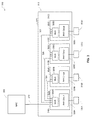
- FIG. 3 illustrates an example multi-chip module with a high-rate interface according to some aspects of the subject technology.
- FIG. 4 illustrates an example single-port Ethernet system according to some aspects of the subject technology.
- FIG. 5 illustrates an example programmable multiplexer according to some aspects of the subject technology.
- FIG. 6 illustrates an example media access control (MAC) device according to some aspects of the subject technology.
- MAC media access control
- FIG. 7 illustrates an example multi-chip module with multiple interfaces according to some aspects of the subject technology.
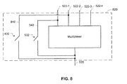
- FIG. 8 illustrates an example programmable multiplexer according to some aspects of the subject technology.
- FIG. 9 illustrates a multi-chip module according to some aspects of the subject technology.
- FIG. 1 shows an example of an Ethernet system 100 that may be used in an access point to provide a computing device with access to an Ethernet network.
- the Ethernet system 100 includes a media access control (MAC) device 105, a single-port physical layer device (PHY) 110, and a connector 130 (e.g., RJ-45 connector) that connects the Ethernet system 100 to an Ethernet cable (not shown).
- the Ethernet cable may include wires (e.g., copper wires) or optical fibers. In some implementations, the Ethernet cable includes four twisted wire pairs.
- the MAC device 105 implements data-link layer (OSI layer 2) processing of data, including encapsulation of data into frames and media access management.
- the MAC device 105 outputs a data stream to the PHY 110 via a MAC/PHY interface 115 (e.g., a serial gigabit media independent interface (SGMII)).
- the PHY 110 may perform physical-layer (OSI layer 1) processing on the data stream from the MAC device 105 to convert the data stream into a physical-layer data signal for transmission on the Ethernet cable.
- the physical layer may include a physical coding sublayer and a physical medium dependent sublayer.
- the physical-layer data signal from the PHY 110 is output to the Ethernet cable via the connector 130.
- FIG. 2 shows an example of an Ethernet system 200 that may be used in a multi-port Ethernet switch to connect multiple devices to an Ethernet network.
- the Ethernet system 200 includes a MAC device 205, a quad-port PHY 210, and four connectors 230A-230D (e.g., four RJ-45 connectors) that connect the Ethernet system 200 to four separate Ethernet cables (not shown).
- the MAC device 205 implements data-link layer (OSI layer 2) processing of data, including encapsulation of data into frames and media access management.
- the MAC device 205 may receive data to be transmitted on the four Ethernet cables to different computing devices, and process the data at the data-link layer into four data streams, where each data stream is to be transmitted on a different one of the Ethernet cables.
- the MAC device 205 may multiplex the data streams into a multiplexed data stream (e.g., a serial multiplexed data stream), and output the multiplexed data stream to the quad-port PHY 210 via a MAC/PHY interface 215 (e.g., a quad SGMII (QSGMII)).
- QSGMII quad SGMII
- each data stream may have a data rate of approximately 1 Gbit/s and the multiplexed data stream may have a data rate of approximately 4 Gbit/s.
- the quad-port PHY 210 includes a multiplexer (MUX) 220, and four physical layer (PHY) circuits 225A-225D.
- the MUX 220 demultiplexes the multiplexed data stream from the MAC device 205 into the four data streams.
- the MUX 220 may demultiplex a QSGMII data stream into four SGMII data streams.
- the MUX 220 outputs each data stream to a different one of the PHY circuits 225A-225D.
- Each PHY circuit 225A-225D performs physical-layer (OSI layer 1) processing on the respective data stream to convert the data stream into a physical-layer data signal for transmission on the respective Ethernet cable.
- Each PHY circuit 225A-225D outputs the respective physical-layer data signal to the respective Ethernet cable via the respective connector 230A-230D (e.g., RJ-45 connector).
- the quad-port PHY 210 may be integrated on a single chip.
- An advantage of integrating the quad-port PHY 210 is that it reduces the number of off-chip I/Os in an Ethernet switch. This is because the quad-port PHY 210 uses a single high-speed MAC/PHY interface to communicate with the MAC device 205.
- a PHY chip manufacturer may separately develop a single-port PHY chip and a multi-port PHY chip (e.g., a quad-port PHY chip).
- a multi-port PHY chip e.g., a quad-port PHY chip
- FIG. 3 illustrates an example multi-port system 300 including a multi-chip module (MCM) 312 according to aspects of the subject technology.
- the MCM 312 includes a first single-port PHY 310A, a second single-port PHY 310B, a third single-port PHY 310C, and a fourth single-port PHY 310D.
- Each single-port PHY 310A-310D may be integrated on a separate chip or die, and may be identical.
- the single-port PHYs 310A-310D may be mounted on a common substrate 315, such as a ceramic substrate, and/or another type of substrate to form the MCM 312.
- Each single-port PHY 310A-310D includes a MUX 320A-320D and a PHY circuit 325A-325D for performing physical-link layer processing.
- Each single-port PHY 310A-310D is connected to a respective Ethernet cable (not shown) via a respective connector 330A-330D (e.g., RJ-45 connector).
- the first single-port PHY 320A is connected to the MAC device 205 via a high-speed MAC/PHY interface 215.
- the first single-port PHY 320A is connected to the second, third and fourth single-port PHYs 310B, 310C and 310D via lower-speed interfaces 324, 326 and 328, respectively, as shown in FIG. 3 .
- the interfaces 324, 326 and 328 interconnect the PHYs 310A-310D of the MCM 312. Any of the lower-speed interfaces 324, 326 and 328 may include a conductive trace on the substrate 315.
- the MAC device 205 receives data to be transmitted on the four Ethernet cables, processes the data at the data-link layer into four data streams, and multiplexes the data streams into a multiplexed data stream (e.g., a serial multiplexed data stream).
- the multiplexed data stream is output to the first single-port PHY 310A via the MAC/PHY interface 215.
- the MAC device 205 may multiplex the data streams by interleaving the bits or bytes of the data streams.
- the MAC device 205 may use another multiplexing technique, including, but to limited to, frequency division multiplexing, code division multiplexing, etc.
- the MUX 320A of the first single-port PHY 310A demultiplexes the multiplexed data stream into the four data streams. Each demultiplexed data stream may have a data rate equal to one-fourth the data rate of the multiplexed data stream.
- the MUX 320A outputs one of the data streams to the respective PHY circuit 325A on the same chip.
- the PHY circuit 325A performs physical-layer (OSI layer 1) processing on the data stream to convert the data stream into a physical-layer data signal for transmission on the respective Ethernet cable via connector 330A.
- OSI layer 1 physical-layer
- the MUX 320A of the first single-port PHY 310A outputs each of the other three data streams to a different one of the second, third and fourth single-port PHYs 310B-310D via the respective interface 324, 326 and 328.
- the MUX 320B-320D in each of the second, third and fourth single-port PHYs 310B-310D passes the received data stream to the respective PHY circuit 325B-325D.
- Each PHY circuit 325B-325D performs physical-layer (OSI layer 1) processing on the respective data stream to convert the data stream into a physical-layer data signal for transmission on the respective Ethernet cable via the respective connector 330B-330D.
- OSI layer 1 physical-layer
- the single-port PHY that receives the multiplexed data stream from the MAC device 205, demultiplexes the multiplexed data stream, and outputs the demutiplexed data streams to other PHYs in the MCM 312 may be referred to as a master PHY.
- Each of the other single-port PHYs that receives a data stream from the master PHY may be referred to as a slave PHY.
- the first single-port PHY 310A acts as a master PHY and the second, third and fourth single-port PHYs 310B-310D act as slave PHYs.
- the MUX 320A-320D in each of the single-ports PHY 310A-310D may have the capability of demultiplexing a multiplexed data stream from the MAC device 205 into demultiplexed data streams.
- this capability of the respective MUX may be unused, in which case the respective MUX may simply pass a received data stream to the respective PHY circuit.
- any of the MUXs 320A-320D may be implemented using a programmable MUX that can be selectively programmed to operate in one of a first mode and a second mode.
- the MUX demultiplexs a multiplexed data stream from the MAC device 205 into multiple data streams, and, in the second mode, the MUX passes a received data stream to the respective PHY circuit.
- the MUX may be programmed in operate in the first mode or the second mode depending on whether the respective single-port PHY is to be used as a master or a slave.
- each of the single-port PHYs 310A-310D may be capable of acting as a master PHY or a slave PHY.
- a single-port PHY acts as a slave PHY
- three of the I/Os of the respective MUX are not used since they are not needed to output demultiplexed data streams to the other PHYs.
- three of the I/Os 322B of the second single-port PHY 310B are unused
- three of the I/Os 322C of the third single-port PHY 310C are unused
- three of the I/Os 322D of the fourth single-port PHY 310D are unused. All three of the corresponding I/Os 322A of the first single-port PHY 310A are used to output demultiplexed data streams to the other singe-port PHYs.
- the subject technology allows a multi-port MCM 312 with one interface to the MAC device 205 to be created using multiple single-port PHYs 310A-310D, each of which can be on a separate chip.
- any of the single-port PHYs 310A-310D may be used in a single-port system (e.g., access point).
- FIG. 4 shows an example in which the first single-port PHY 310A is used in a single-port Ethernet system 400 (e.g., an access point).
- the MUX 320A of the first single-port PHY 310A may receive a data stream from a MAC device 405 via a MAC/PHY interface 415, and pass the received data stream to the respective PHY circuit 325A for physical-layer processing.
- the demultiplexing function of the MUX 320A is not used, and three of the I/Os 322A of the MUX 320A are not used.
- the subject technology allows one type of chip to be used in multi-port and single-port applications.
- the subject technology allows one chip development to address both the multi-port market (e.g., Ethernet switch) and single-port market (e.g., access point) markets, thereby reducing development costs.
- the MCM 312 is described above using the example of four single-port PHYs, it is to be appreciated that the subject technology is not limit to this example, and that the MCM 312 may include any number of single-port PHYs.
- the MCM 312 may include N single-port PHYs, in which N is an integer and the MAC device 205 multiplexes N data streams into a multiplexed data stream.
- the MUX in a first one of the single-port PHYs s may demultiplex the multiplexed data stream into the N data streams, output one of the N data streams to the respective PHY circuit for physical-layer processing, and output each of the other data streams to a different one of the other single-port PHYs.
- FIG. 5 illustrates a programmable MUX 520 according to some aspects of the subject technology.
- the programmable MUX 520 may be used to implement any one of the MUXs 320A-320D.
- the programmable MUX 520 may be coupled to four I/Os 522-1 to 522-4 of the respective single-port PHY. I/Os 522-1 and 522-4 may couple the MUX 520 to separate external pins or contacts (not shown) of the respective single-port PHY for connection to other single-port PHYs and/or a MAC device.
- the programmable MUX 520 includes a multiplexer 530, a connection 535 to the respective PHY circuit, and a switch 532 connected between I/O 522-1 and the PHY circuit.
- the multiplexer 530 may be configured to receive a multiplexed data stream on I/O 522-1, demultiplex the multiplexed data stream into four data streams, output one of the demultiplxed data streams to the respective PHY circuit via connection 535, and output each of the other demultiplexed data streams to a different one of I/Os 522-2 to 522-4.
- the programmable MUX 520 may be selectively programmed to operate in one of a first mode and a second mode. In the first mode, the MUX 520 demultiplexes a multiplexed data stream. The MUX 520 may be programmed to operate in the first mode by opening switch 532 and powering on the multiplexer 530. When the MUX 520 is to operate in the first mode, I/O 522-1 may be connected to the MAC device 205 via a MAC/PHY interface 215, and each of I/Os 522-2 to 522-4 may be connected to a different one of the other single-port PHYs on the MCM 312.
- the multiplexer 530 receives a multiplexed data stream from the MAC device 205 via I/O 522-1, demultiplexes the multiplexed data stream, outputs one of the demultiplxed data streams to the respective PHY circuit via connection 535, and outputs each of the other demultiplexed data streams to a different one of the other single-port PHYs via the respective I/O 522-2 to 522-4.
- the MUX 520 passes a received data stream to the respective PHY circuit.
- the MUX 520 may be programmed to operate in the second mode by closing switch 532 and powering off the multiplexer 530. Closing the switch 532 creates a path 540 between I/O 522-1 and the respective PHY circuit, bypassing the multiplexer 530.
- I/O 522-1 may be connected to a master single-port PHY or a MAC device.
- the MUX 520 receives a data stream on I/O 522-1 from a master PHY or a MAC device, and passes the received data stream to the respective PHY circuit via path 540 and connection 535.
- FIG. 6 illustrates a MAC device 605 that may be used with the MCM 312 according to aspects of the subject technology.
- the MAC device 605 includes four MAC circuits 610A-610D and a multiplexer (MUX) 612.
- Each MAC circuit 610A-610D performs data-link layer (OSI layer 2) processing on data to be transmitted on a different one of the Ethernet cables, and outputs a data stream to the MUX 612.
- the MUX 612 multiplexes the data streams from the MAC circuits 610A-610D into a multiplexed data stream, and outputs the multiplexed data stream to the MCM 312 via a MAC/PHY interface 615.
- OSI layer 2 data-link layer
- the MUX 320A of the first single-port PHY 310A demultiplexes the multiplex data stream into the four data streams corresponding to MAC circuits 610A-610D.
- the MUX 320A of the first single-port PHY 310A outputs the data stream corresponding to MAC circuit 610A to the respective PHY circuit 325A for physical-layer processing, and outputs the data streams corresponding to MAC circuits 610B, 610C and 610D to the second, third and fourth single-port PHYs 610B, 610C and 610D, respectively.
- Each single-port PHY performs physical-layer (OSI layer 1) processing on the respective data stream.
- the MUX 612 may multiplex the data streams from MAC circuits 610A-610D using bit-interleaved multiplexing or byte-interleaved multiplexing.
- bit-interleaved multiplexing the MUX 612 interleaves the bits of the data streams, in which the bits of a particular data stream appear in every fourth bit of the multiplexed data stream. The MUX 612 may do this by sequentially outputting a first bit from each data stream, then sequentially outputting a second bit from each data stream, and so forth.
- the MUX 320A of the first single-port PHY 3 l0A may demultiplex the multiplexed data stream by de-interleaving the bits of the multiplexed data stream into the four data streams. For example, the MUX 320A may output a demultiplexed data stream at one of the outputs of the MUX 320A by outputting every fourth bit in the multiplexed data stream to that output.
- the MUX 612 interleaves the bytes of the data streams, in which the bytes of a particular data stream appear in every fourth byte of the multiplexed data stream.
- Each byte may be made up of 8 bits, 10 bits or another number of bits.
- the MUX 612 may do this by sequentially outputting a first byte from each data stream, then sequentially outputting a second byte from each data stream, and so forth.
- the MUX 320A of the first single-port PHY 310A may demultiplex the multiplexed data stream by de-interleaving the bytes of the multiplexed data stream into the four data streams. For example, the MUX 320A may output a demultiplexed data stream at one of the outputs of the MUX 320A by outputting every fourth byte in the multiplexed data stream to that output.
- the MAC device 605 is described above using the example of four MAC circuits 610A-610D, it is to be appreciated that the subject technology is not limit to this example, and that the MAC device 605 may include any number of MAC circuits. Generally speaking, the MAC device 605 may include N MAC circuits that output N data streams, in which N is an integer and the MUX 612 multiplexes the N data streams into a multiplexed data stream.
- each PHY circuit 325A-325D may output data to the respective Ethernet cable at a data rate of approximately 2.5 Gbit/s.
- Each PHY circuit 325A-325D may achieve a data rate of approximately 2.5 Gbit/s by modulating data using double square (DSQ) 128 modulation or other high-level modulation scheme.
- DSQ double square
- Any of the Ethernet cables may be a CAT 5e cable, a CAT 6 cable, or another type of cable.
- the MAC device 205 may output the multiplexed data stream at a data rate of approximately 10 Gbit/s, and the MUX 320A of the first single-port PHY 310A may demultiplex the multiplexed data stream into four data streams, where each data stream has a data rate of approximately 2.5 Gbit/s.
- the MUX 320 may output one of the data streams to the respective PHY circuit 325A, and output each of the other three data streams to a different one of the second, third and fourth single-port PHYs 310B-310D via the respective interface 324, 326 and 328.
- the single-port PHYs 310A-310D may also receive data from the respective Ethernet cables.
- the single-port PHYs 310A-310D may be bi-directional.
- the PHY circuit may perform physical layer (OSI layer 1) processing on the received physical-layer data signal to convert the physical-layer data signal into a data stream.
- OSI layer 1 physical layer
- the MUX 320B-320D in each of the second, third and fourth single-port PHYs 310B-310D may output the respective data stream to the MUX 320A of the first single-port PHY 310A via the respective interface 324, 326 and 328.
- the MUX 320A in the first single-port PHY 310A may multiplex the data stream from the respective PHY circuit 325A with the data streams from the other single-port PHYs 310B-310D into a multiplexed data stream, and output the multiplexed data stream to the MAC device 205 via the MAC/PHY interface 215.
- the MCM 312 may also be connected to multiple MAC devices via multiple MAC/PHY interfaces.
- FIG. 7 shows an example multi-port system 700 including four MAC devices 705A-705D connected to the single-port PHYs 310A-310D of the MCM 312 via separate MAC/PHY interfaces 715A-715D, respectively.
- Each MUX 320A-320D receives a data stream from the respective MAC device 705A-705D via the respective MAC/PHY interface 715A-715D, and passes the received data stream to the respective PHY circuit 325A-325D for physical-layer processing.
- the interfaces 324, 326 and 328 connecting the first single-port PHY 310A to the second, third and fourth single-port PHYs 310B-310D, respectively, are not used.
- Each MUX 320A-320D may be implemented using a programmable MUX that can be programmed to pass a data stream received on any I/O of the MUX to the respective PHY circuit for physical-layer processing.
- the MUX 320A-320D is each single-port PHY 310A-310D may be programmed to pass a data stream received on the I/O connected to the respective MAC/PHY interface 715A-715D to the respective PHY circuit 325A-325D.
- each single-port PHYs 310A-310D may operate independently, and the electrical interconnections (i.e., interfaces 324, 326 and 328) between the single-port PHYs 310A-310D are not used.
- the MUX 320A in the first single-port PHY 310A may be programmed to demultiplex a multiplex data stream received on the I/O connected to the MAC/PHY interface 215, output one of the demultiplexed data streams to the respective PHY circuit 325A, and output each of the other demultiplexed data streams to a different one of the three I/Os connected to the interfaces 324, 326 and 328.
- the MUX 320B-320D in each of the second, third and fourth single-port PHYs 310B-310D may be programmed to pass a data stream received on the I/O connected to the respective interface 324, 326 and 328 to the respective PHY circuit 325B-325D.
- the MCM 312 may be connected to a MAC device 205 via a single high-rate MAC/PHY interface or connected to multiple MAC devices 705A-705D via separate lower-rate MAC/PHY interfaces 715A-715D. This provides the MCM 312 with the flexibility of being used in different system configurations.
- FIG. 8 illustrates a programmable MUX 820 according to some aspects of the subject technology.
- the programmable MUX 820 is similar to the programmable MUX 520 in FIG. 5 , and further includes a second switch 832 connected between I/O 522-2 and connection 535 to the respective PHY circuit.
- the second switch 832 When the programmable MUX 820 is used to demultiplex a multiplexed data stream from the MAC device 205 or pass a data stream received on I/O 522-1 to the respective PHY circuit, the second switch 832 may be open. When the programmable MUX 820 is used to pass a data stream received from the respective MAC device 705A-705D in the system 700 in FIG. 7 , I/O 522-2 may be connected to the respective MAC device 705A-705D via the respective MAC/PHY interface 715A-715D, the second switch 832 may be closed, the first switch 532 may be open, and the multiplexer 530 may be powered off.
- closing the second switch 832 creates a path 840 between I/O 522-2 and the respective PHY circuit that bypasses the multiplexer 530.
- a data stream received from the respective MAC device on I/O 522-2 is passed to the respective PHY circuit.
- FIG. 9 illustrates an example multi-port system 900 including a multi-chip module (MCM) 912 according to aspects of the subject technology.
- the MCM 912 includes a first single-port PHY 910A, a second single-port PHY 910B, a third single-port PHY 910C, and a fourth single-port PHY 910D.
- Each single-port PHY 910A-910D may be integrated on a separate chip or die, and may be identical.
- the single-port PHYs 910A-910D may be mounted on a common substrate 914 to form the MCM 912.
- Each single-port PHY 910A-910D includes a packet router 920A-920D and a PHY circuit 925A-925D for performing physical-link layer processing.
- Each single-port PHY 910A-910D is connected to a respective Ethernet cable (not shown) via a respective connector 930A-930D (e.g., RJ-45 connector).
- the first single-port PHY 920A is connected to the MAC device 905 via a high-speed MAC/PHY interface 915.
- the first single-port PHY 320A is connected to the second, third and fourth single-port PHYs 910B, 910C and 910D via lower-speed interfaces 924, 926 and 928, respectively, as shown in FIG. 9 .
- the MAC device 905 receives data to be transmitted on the four Ethernet cables to four different computing devices (e.g., VoIP devices, access points, etc.).
- the MAC device 905 processes the data for each computing device into data packets, where each packet may include an address identifying the computing device as a destination of the packet.
- a data packet may also be referred to as a frame.
- the MAC device 905 outputs the data packets for the different computing devices to the MCM 912 via the interface 915.
- the MAC device 905 may output the data packets for the different computing devices one packet at a time. For example, the MAC device 905 may interleave the data packets for the different computing devices and output the interleaved packets to the MCM 912 via the interface 915.
- the data packets for the different computing devices may have different sizes.
- the MAC device 905 may manage the data packet traffic such that the data rate (number of bits per unit of time) for each computing device is approximately the same.
- the MAC device 905 may implement a traffic policy in which each computing device (and hence respective PHY) is allocated approximately an equal share of the total data rate of the interface 915.
- the MAC device 905 may include a buffer that temporarily stores data packets for the different computing devices. The MAC device 905 may then output the data packets in the buffer to the interface 915 in an order that results in approximately equal data rates for the computing devices. For example, if large data packets are addressed to a first one of the computing devices and smaller packets are addressed to a second one of the computing devices, then the MAC device 905 may output several packets addressed to the second computing device for every packet addressed to the first device such that the data rates for the devices are approximately equal.
- the MAC device 905 may manage the data packet traffic such that the data rate for each computing device is approximately 2.5 Gbits/s.
- the data rate of the interface 915 may be 10 Gbits/s.
- the router 920A of the first single-port PHY 910A looks at the addresses of incoming data packets from the MAC device 905, and routes the data packets accordingly. If a packet is addressed to a computing device corresponding to the first single-port PHY 910A, the router 920A routes the data packet to the respective PHY circuit 925A for physical-layer processing. If a packet is addressed to a computing device corresponding to the second single-port PHY 910B, the router 920A routes the data packet to the second single-port PHY 910B via the respective interface 924.
- the router 920A routes the data packet to the third single-port PHY 910C via the respective interface 926. If a packet is addressed to a computing device corresponding to the fourth single-port PHY 910D, the router 920A routes the data packet to the fourth single-port PHY 910D via the respective interface 928.
- the router 920B-920D in each of the second, third and fourth single-port PHYs 910B-910D passes received packets to the respective PHY circuit 925B-925D.
- Each PHY circuit 925B-925D performs physical-layer (OSI layer 1) processing on the respective data packets to convert the data packets into a physical-layer data signal for transmission to the respective computing device via the respective Ethernet cable.
- OSI layer 1 physical-layer
- the router 920A-920D in each of the single-port PHYs 910A-910D may have the capability of routing each data packet from the MAC device 905 to the respective PHY circuit or another single-port PHY based on the address of the packet.
- the address routing functionality of the respective router may be turned off, in which case the respective router may simply pass a received data packet to the respective PHY circuit without looking at the address of the packet.
- each router 920A-920D may be configured to be selectively programmed to operate in one of a first mode and a second mode.
- the router may be configured to route data packets based on addresses of the data packets. For example, the router may route packets addressed to a computing device corresponding to the corresponding single-port PHY to the respective PHY circuit, and route packets addressed to other computing devices to the corresponding single-port PHYs.
- the router In the second mode, the router may be configured to pass data packets received from a master PHY or a MAC device to the respective PHY without looking at the addresses of the packets.
- each of the single-port PHYs 910A-910D may be capable of acting as a master PHY or a slave PHY.
- a single-port PHY acts as a slave PHY
- three of the I/Os of the respective router are not used since they are not needed to route packets to the other PHYs.
- three of the I/Os 922B of the second single-port PHY 910B are unused
- three of the I/Os 922C of the third single-port PHY 910C are unused
- three of the I/Os 922D of the fourth single-port PHY 910D are unused. All three of the corresponding I/Os 922A of the first single-port PHY 910A are used to route packets to the other singe-port PHYs.
- the functions described above can be implemented in digital electronic circuitry, in computer software, firmware or hardware.
- the techniques can be implemented using one or more computer program products.
- Programmable processors and computers can be included in or packaged as mobile devices.
- the processes and logic flows can be performed by one or more programmable processors and by one or more programmable logic circuitry.
- Some implementations can include electronic components, such as microprocessors, storage and memory that store computer program instructions in a machine-readable or computer-readable medium (alternatively referred to as computer-readable storage media, machine-readable media, or machine-readable storage media).
- computer-readable media include RAM, ROM, read-only compact discs (CD-ROM), recordable compact discs (CD-R), rewritable compact discs (CD-RW), read-only digital versatile discs (e.g., DVD-ROM, dual-layer DVD-ROM), a variety of recordable/rewritable DVDs (e.g., DVD-RAM, DVD-RW, DVD+RW, etc.), flash memory (e.g., SD cards, mini-SD cards, micro-SD cards, etc.), magnetic and/or solid state hard drives, ultra density optical discs, any other optical or magnetic media, and floppy disks.
- CD-ROM read-only compact discs
- CD-R recordable compact discs
- CD-RW rewr
- the computer-readable media can store a computer program that is executable by at least one processing unit and includes sets of instructions for performing various operations.
- Examples of computer programs or computer code include machine code, such as is produced by a compiler, and files including higher-level code that are executed by a computer, an electronic component, or a microprocessor using an interpreter.
- Some implementations can be performed by a microprocessor or multi-core processors that execute software. Some implementations can be performed by one or more integrated circuits, such as application specific integrated circuits (ASICs) or field programmable gate arrays (FPGAs). In some implementations, such integrated circuits can execute instructions that are stored on the circuit itself.
- ASICs application specific integrated circuits
- FPGAs field programmable gate arrays
- Computer readable storage medium also referred to as computer readable medium.
- processing unit(s) e.g., one or more processors, cores of processors, or other processing units
- Examples of computer readable media include, but are not limited to, CD-ROMs, flash drives, RAM chips, hard drives, EPROMs, etc.
- the computer readable media does not include carrier waves and electronic signals passing wirelessly or over wired connections.
- a processor configured to monitor and control an operation or a component may also mean the processor being programmed to monitor and control the operation or the processor being operable to monitor and control the operation.
- a processor configured to execute code can be construed as a processor programmed to execute code or operable to execute code.
- a phrase such as an "aspect” does not imply that such aspect is essential to the subject technology or that such aspect applies to all configurations of the subject technology.
- a disclosure relating to an aspect may apply to all configurations, or one or more configurations.
- a phrase such as an aspect may refer to one or more aspects and vice versa.
- a phrase such as a “configuration” does not imply that such configuration is essential to the subject technology or that such configuration applies to all configurations of the subject technology.
- a disclosure relating to a configuration may apply to all configurations, or one or more configurations.
- a phrase such as a configuration may refer to one or more configurations and vice versa.
- example is used herein to mean “serving as an example or illustration.” Any aspect or design described herein as “example” is not necessarily to be construed as preferred or advantageous over other aspects or designs.
Landscapes
- Engineering & Computer Science (AREA)
- Computer Networks & Wireless Communication (AREA)
- Signal Processing (AREA)
- Microelectronics & Electronic Packaging (AREA)
- Small-Scale Networks (AREA)
- Time-Division Multiplex Systems (AREA)
- Data Exchanges In Wide-Area Networks (AREA)
Abstract
Description
- The present description relates generally to multi-chip modules, and more particularly, to multi-chip modules with a high-rate interface.
- Ethernet is widely used to transport voice, data and multimedia traffic between computing devices because of its high speed, relatively low cost, and ease of installation. A computing device (e.g., a voice over Internet (VoIP) device, a network camera, a computer, etc.) may be connected to an Ethernet switch or an access point by an Ethernet cable, and may communicate with another computing device via the Ethernet switch or access point.
- According to an aspect, a multi-chip module comprises:
- a substrate;
- a first physical-layer (PHY) chip mounted on the substrate, the first PHY chip comprising a multiplexer and a physical-layer (PHY) circuit;
- a second PHY chip mounted on the substrate; and
- an interface coupling the first PHY chip to the second PHY chip;
- wherein the multiplexer of the first PHY chip is configured to receive a multiplexed data stream from a media access control (MAC) device, to demultiplex the multiplexed data stream into a first data stream and a second data stream, to output the first data stream to the PHY circuit of the first PHY chip, and to output the second data stream to the second PHY chip via the interface.
- Advantageously, the multiplexer is configured to demultiplex the multiplexed data stream by de-interleaving bytes or bits in the multiplexed data stream.
- Advantageously, the multi-chip module further comprises:
- a third PHY chip mounted on the substrate;
- a fourth PHY chip mounted on the substrate;
- a second interface coupling the first PHY chip to the third PHY chip; and
- a third interface coupling the first PHY chip to the fourth PHY chip;
- wherein the multiplexer of the first PHY chip is further configured to demultiplex the multiplexed data stream into a third data stream and a fourth data stream, to output the third data stream to the third PHY chip via the second interface, and to output the fourth data stream to the fourth PHY chip via the third interface.
- Advantageously, the first data stream has a data rate that is approximately one-fourth a data rate of the multiplexed data stream.
- Advantageously, the multiplexed data stream has a data rate of approximately 10 Gbits per second, and each of the first, second, third and fourth data streams has a data rate of approximately 2.5 Gbits per second.
- Advantageously, the second PHY chip comprises a second multiplexer and a second PHY circuit, and wherein the second multiplexer is configured to receive the second data stream from the first PHY chip via the first interface, and to pass the second data stream to the second PHY circuit.
- Advantageously, the second multiplexer is configured to selectively operate in one of a first mode and a second mode, in the first mode, the second multiplexer is configured to demultiplex a multiplexed data stream, in the second mode, the second multiplexer is configured to pass the second data stream to the second PHY circuit, and the second multiplexer is programmed to operate in the second mode.
- Advantageously, the first PHY chip and the second PHY chip are substantially identical.
- Advantageously, the first PHY circuit is configured to convert the first data stream into a first physical-layer data signal for transmission on a first Ethernet cable, and the second PHY circuit is configured to convert the second data stream into a second physical-layer data signal for transmission on a second Ethernet cable.
- According to an aspect, a physical-layer (PHY) chip comprises:
- a multiplexer configured to selectively operate in one of a first mode and a second mode; and
- a PHY circuit;
- wherein, in the first mode, the multiplexer is configured to demultiplex a multiplexed data stream received by the PHY chip into a first data stream and a second data stream, to output the first data stream to the PHY circuit, and to output the second data stream to another PHY chip, and, in the second mode, the multiplexer is configured to pass a data stream received by the PHY chip to the PHY circuit;
- wherein the PHY circuit is configured to convert a data stream from the multiplexer into a physical-layer data signal for transmission on an Ethernet cable.
- Advantageously, the multiplexer is configured to demultiplex the multiplexed data stream by de-interleaving bytes or bits in the multiplexed data stream.
- Advantageously, the PHY chip further comprises:
- a first input/output (I/O) coupled to the multiplexer; and
- a second I/O coupled to the multiplexer;
- wherein, in the first mode, the multiplexer is configured to receive the multiplexed data stream on the first I/O, and to output the second data stream to the other PHY chip on the second I/O, and, in the second mode, the multiplexer is configured to pass a data stream received on the first I/O to the PHY circuit.
- Advantageously, the multiplexer is further configured to selectively operate in a third mode, and wherein, in the third mode, the multiplexer is configured to pass a data stream received on the second I/O to the PHY circuit.
- According to an aspect, a multi-chip module comprises:
- a substrate;
- a first physical-layer (PHY) chip mounted on the substrate, the first PHY chip comprising a router and a physical-layer (PHY) circuit;
- a second PHY chip mounted on the substrate; and
- an interface coupling the first PHY chip to the second PHY chip;
- wherein the router of the first PHY chip is configured to receive a plurality of data packets from a media access control (MAC) device, to route one or more of the plurality of data packets having a first address to the PHY circuit, and to route one or more of the plurality of data packets having a second address to the second PHY chip via the interface.
- Advantageously, the multi-chip module further comprises:
- a third PHY chip mounted on the substrate;
- a fourth PHY chip mounted on the substrate;
- a second interface coupling the first PHY chip to the third PHY chip; and
- a third interface coupling the first PHY chip to the fourth PHY chip;
- wherein the router of the first PHY chip is further configured to route one or more of the plurality of data packets having a third address to the third PHY chip via the second interface, and to route one or more of the plurality of data packets having a fourth address to the fourth PHY chip via the third interface.
- Advantageously, the second PHY chip comprises a second router and a second PHY circuit, and wherein the second router is configured to pass data packets received from the first PHY chip via first interface to the second PHY circuit.
- Advantageously, the second router is configured to selectively operate in one of a first mode and a second mode, in the first mode, the second router is configured to route data packets based on addresses of the data packets, in the second mode, the second router is configured to pass data packets from the first PHY chip to the second PHY circuit, and the second router is programmed to operate in the second mode.
- Advantageously, the first PHY chip and the second PHY chip are substantially identical.
- Advantageously, in the second mode, the router is configured to pass the data packets from the first PHY chip to the second PHY circuit without looking at addresses in the data packets.
- Advantageously, the first PHY circuit is configured to convert data packets from the first router into a first physical-layer data signal for transmission on a first Ethernet cable, and the second PHY circuit is configured to convert data packets from the second router into a second physical-layer data signal for transmission on a second Ethernet cable.
- Certain features of the subject technology are set forth in the appended claims. However, for purpose of explanation, several embodiments of the subject technology are set forth in the following figures.
-
FIG. 1 illustrates an example of an Ethernet system that includes a single-port physical layer (PHY) chip. -
FIG. 2 illustrates an example of an Ethernet system that includes a multi-port physical layer (PHY) chip. -
FIG. 3 illustrates an example multi-chip module with a high-rate interface according to some aspects of the subject technology. -
FIG. 4 illustrates an example single-port Ethernet system according to some aspects of the subject technology. -
FIG. 5 illustrates an example programmable multiplexer according to some aspects of the subject technology. -
FIG. 6 illustrates an example media access control (MAC) device according to some aspects of the subject technology. -
FIG. 7 illustrates an example multi-chip module with multiple interfaces according to some aspects of the subject technology. -
FIG. 8 illustrates an example programmable multiplexer according to some aspects of the subject technology. -
FIG. 9 illustrates a multi-chip module according to some aspects of the subject technology. - The detailed description set forth below is intended as a description of various configurations of the subject technology and is not intended to represent the only configurations in which the subject technology may be practiced. The appended drawings are incorporated herein and constitute a part of the detailed description. The detailed description includes specific details for the purpose of providing a thorough understanding of the subject technology. However, the subject technology is not limited to the specific details set forth herein and may be practiced without one or more of the specific details. In some instances, structures and components are shown in block diagram form in order to avoid obscuring the concepts of the subject technology.
-
FIG. 1 shows an example of anEthernet system 100 that may be used in an access point to provide a computing device with access to an Ethernet network. TheEthernet system 100 includes a media access control (MAC)device 105, a single-port physical layer device (PHY) 110, and a connector 130 (e.g., RJ-45 connector) that connects theEthernet system 100 to an Ethernet cable (not shown). The Ethernet cable may include wires (e.g., copper wires) or optical fibers. In some implementations, the Ethernet cable includes four twisted wire pairs. - The
MAC device 105 implements data-link layer (OSI layer 2) processing of data, including encapsulation of data into frames and media access management. TheMAC device 105 outputs a data stream to thePHY 110 via a MAC/PHY interface 115 (e.g., a serial gigabit media independent interface (SGMII)). ThePHY 110 may perform physical-layer (OSI layer 1) processing on the data stream from theMAC device 105 to convert the data stream into a physical-layer data signal for transmission on the Ethernet cable. The physical layer may include a physical coding sublayer and a physical medium dependent sublayer. The physical-layer data signal from thePHY 110 is output to the Ethernet cable via theconnector 130. -
FIG. 2 shows an example of anEthernet system 200 that may be used in a multi-port Ethernet switch to connect multiple devices to an Ethernet network. TheEthernet system 200 includes aMAC device 205, a quad-port PHY 210, and fourconnectors 230A-230D (e.g., four RJ-45 connectors) that connect theEthernet system 200 to four separate Ethernet cables (not shown). - The
MAC device 205 implements data-link layer (OSI layer 2) processing of data, including encapsulation of data into frames and media access management. TheMAC device 205 may receive data to be transmitted on the four Ethernet cables to different computing devices, and process the data at the data-link layer into four data streams, where each data stream is to be transmitted on a different one of the Ethernet cables. TheMAC device 205 may multiplex the data streams into a multiplexed data stream (e.g., a serial multiplexed data stream), and output the multiplexed data stream to the quad-port PHY 210 via a MAC/PHY interface 215 (e.g., a quad SGMII (QSGMII)). For QSGMII implementations, each data stream may have a data rate of approximately 1 Gbit/s and the multiplexed data stream may have a data rate of approximately 4 Gbit/s. - The quad-
port PHY 210 includes a multiplexer (MUX) 220, and four physical layer (PHY)circuits 225A-225D. TheMUX 220 demultiplexes the multiplexed data stream from theMAC device 205 into the four data streams. For QSGMII implementations, theMUX 220 may demultiplex a QSGMII data stream into four SGMII data streams. TheMUX 220 outputs each data stream to a different one of thePHY circuits 225A-225D. EachPHY circuit 225A-225D performs physical-layer (OSI layer 1) processing on the respective data stream to convert the data stream into a physical-layer data signal for transmission on the respective Ethernet cable. EachPHY circuit 225A-225D outputs the respective physical-layer data signal to the respective Ethernet cable via therespective connector 230A-230D (e.g., RJ-45 connector). - The quad-
port PHY 210 may be integrated on a single chip. An advantage of integrating the quad-port PHY 210 is that it reduces the number of off-chip I/Os in an Ethernet switch. This is because the quad-port PHY 210 uses a single high-speed MAC/PHY interface to communicate with theMAC device 205. - To address both the single-port market (e.g., access point market) and the multi-port market (e.g., Ethernet switch market), a PHY chip manufacturer may separately develop a single-port PHY chip and a multi-port PHY chip (e.g., a quad-port PHY chip). However, having separate chip developments to address both markets drives up development costs. Accordingly, it is desirable to develop a PHY chip that can address both markets.
-
FIG. 3 illustrates anexample multi-port system 300 including a multi-chip module (MCM) 312 according to aspects of the subject technology. TheMCM 312 includes a first single-port PHY 310A, a second single-port PHY 310B, a third single-port PHY 310C, and a fourth single-port PHY 310D. Each single-port PHY 310A-310D may be integrated on a separate chip or die, and may be identical. The single-port PHYs 310A-310D may be mounted on acommon substrate 315, such as a ceramic substrate, and/or another type of substrate to form theMCM 312. - Each single-
port PHY 310A-310D includes aMUX 320A-320D and aPHY circuit 325A-325D for performing physical-link layer processing. Each single-port PHY 310A-310D is connected to a respective Ethernet cable (not shown) via arespective connector 330A-330D (e.g., RJ-45 connector). The first single-port PHY 320A is connected to theMAC device 205 via a high-speed MAC/PHY interface 215. In addition, the first single-port PHY 320A is connected to the second, third and fourth single-port PHYs speed interfaces FIG. 3 . Theinterfaces PHYs 310A-310D of theMCM 312. Any of the lower-speed interfaces substrate 315. - In operation, the
MAC device 205 receives data to be transmitted on the four Ethernet cables, processes the data at the data-link layer into four data streams, and multiplexes the data streams into a multiplexed data stream (e.g., a serial multiplexed data stream). The multiplexed data stream is output to the first single-port PHY 310A via the MAC/PHY interface 215. TheMAC device 205 may multiplex the data streams by interleaving the bits or bytes of the data streams. TheMAC device 205 may use another multiplexing technique, including, but to limited to, frequency division multiplexing, code division multiplexing, etc. - The
MUX 320A of the first single-port PHY 310A demultiplexes the multiplexed data stream into the four data streams. Each demultiplexed data stream may have a data rate equal to one-fourth the data rate of the multiplexed data stream. TheMUX 320A outputs one of the data streams to therespective PHY circuit 325A on the same chip. ThePHY circuit 325A performs physical-layer (OSI layer 1) processing on the data stream to convert the data stream into a physical-layer data signal for transmission on the respective Ethernet cable viaconnector 330A. - The
MUX 320A of the first single-port PHY 310A outputs each of the other three data streams to a different one of the second, third and fourth single-port PHYs 310B-310D via therespective interface MUX 320B-320D in each of the second, third and fourth single-port PHYs 310B-310D passes the received data stream to therespective PHY circuit 325B-325D. EachPHY circuit 325B-325D performs physical-layer (OSI layer 1) processing on the respective data stream to convert the data stream into a physical-layer data signal for transmission on the respective Ethernet cable via therespective connector 330B-330D. - The single-port PHY that receives the multiplexed data stream from the
MAC device 205, demultiplexes the multiplexed data stream, and outputs the demutiplexed data streams to other PHYs in theMCM 312 may be referred to as a master PHY. Each of the other single-port PHYs that receives a data stream from the master PHY may be referred to as a slave PHY. In the example inFIG. 3 , the first single-port PHY 310A acts as a master PHY and the second, third and fourth single-port PHYs 310B-310D act as slave PHYs. - The
MUX 320A-320D in each of the single-ports PHY 310A-310D may have the capability of demultiplexing a multiplexed data stream from theMAC device 205 into demultiplexed data streams. When a single-port PHY acts as a slave, this capability of the respective MUX may be unused, in which case the respective MUX may simply pass a received data stream to the respective PHY circuit. - Any of the
MUXs 320A-320D may be implemented using a programmable MUX that can be selectively programmed to operate in one of a first mode and a second mode. In the first mode, the MUX demultiplexs a multiplexed data stream from theMAC device 205 into multiple data streams, and, in the second mode, the MUX passes a received data stream to the respective PHY circuit. The MUX may be programmed in operate in the first mode or the second mode depending on whether the respective single-port PHY is to be used as a master or a slave. - Thus, each of the single-
port PHYs 310A-310D may be capable of acting as a master PHY or a slave PHY. When a single-port PHY acts as a slave PHY, three of the I/Os of the respective MUX are not used since they are not needed to output demultiplexed data streams to the other PHYs. As shown in the example inFIG. 3 , three of the I/Os 322B of the second single-port PHY 310B are unused, three of the I/Os 322C of the third single-port PHY 310C are unused, and three of the I/Os 322D of the fourth single-port PHY 310D are unused. All three of the corresponding I/Os 322A of the first single-port PHY 310A are used to output demultiplexed data streams to the other singe-port PHYs. - Thus, the subject technology allows a
multi-port MCM 312 with one interface to theMAC device 205 to be created using multiple single-port PHYs 310A-310D, each of which can be on a separate chip. In addition, any of the single-port PHYs 310A-310D may be used in a single-port system (e.g., access point). -
FIG. 4 shows an example in which the first single-port PHY 310A is used in a single-port Ethernet system 400 (e.g., an access point). In this example, theMUX 320A of the first single-port PHY 310A may receive a data stream from aMAC device 405 via a MAC/PHY interface 415, and pass the received data stream to therespective PHY circuit 325A for physical-layer processing. In this case, the demultiplexing function of theMUX 320A is not used, and three of the I/Os 322A of theMUX 320A are not used. - Therefore, the subject technology allows one type of chip to be used in multi-port and single-port applications. In other words, the subject technology allows one chip development to address both the multi-port market (e.g., Ethernet switch) and single-port market (e.g., access point) markets, thereby reducing development costs.
- Although the
MCM 312 is described above using the example of four single-port PHYs, it is to be appreciated that the subject technology is not limit to this example, and that theMCM 312 may include any number of single-port PHYs. Generally speaking, theMCM 312 may include N single-port PHYs, in which N is an integer and theMAC device 205 multiplexes N data streams into a multiplexed data stream. The MUX in a first one of the single-port PHYs s may demultiplex the multiplexed data stream into the N data streams, output one of the N data streams to the respective PHY circuit for physical-layer processing, and output each of the other data streams to a different one of the other single-port PHYs. -
FIG. 5 illustrates aprogrammable MUX 520 according to some aspects of the subject technology. Theprogrammable MUX 520 may be used to implement any one of theMUXs 320A-320D. Theprogrammable MUX 520 may be coupled to four I/Os 522-1 to 522-4 of the respective single-port PHY. I/Os 522-1 and 522-4 may couple theMUX 520 to separate external pins or contacts (not shown) of the respective single-port PHY for connection to other single-port PHYs and/or a MAC device. - The
programmable MUX 520 includes amultiplexer 530, aconnection 535 to the respective PHY circuit, and aswitch 532 connected between I/O 522-1 and the PHY circuit. Themultiplexer 530 may be configured to receive a multiplexed data stream on I/O 522-1, demultiplex the multiplexed data stream into four data streams, output one of the demultiplxed data streams to the respective PHY circuit viaconnection 535, and output each of the other demultiplexed data streams to a different one of I/Os 522-2 to 522-4. - The
programmable MUX 520 may be selectively programmed to operate in one of a first mode and a second mode. In the first mode, theMUX 520 demultiplexes a multiplexed data stream. TheMUX 520 may be programmed to operate in the first mode by openingswitch 532 and powering on themultiplexer 530. When theMUX 520 is to operate in the first mode, I/O 522-1 may be connected to theMAC device 205 via a MAC/PHY interface 215, and each of I/Os 522-2 to 522-4 may be connected to a different one of the other single-port PHYs on theMCM 312. - In the first mode, the
multiplexer 530 receives a multiplexed data stream from theMAC device 205 via I/O 522-1, demultiplexes the multiplexed data stream, outputs one of the demultiplxed data streams to the respective PHY circuit viaconnection 535, and outputs each of the other demultiplexed data streams to a different one of the other single-port PHYs via the respective I/O 522-2 to 522-4. - In the second mode, the
MUX 520 passes a received data stream to the respective PHY circuit. TheMUX 520 may be programmed to operate in the second mode by closingswitch 532 and powering off themultiplexer 530. Closing theswitch 532 creates apath 540 between I/O 522-1 and the respective PHY circuit, bypassing themultiplexer 530. When theMUX 520 is to operate in the second mode, I/O 522-1 may be connected to a master single-port PHY or a MAC device. In the second mode, theMUX 520 receives a data stream on I/O 522-1 from a master PHY or a MAC device, and passes the received data stream to the respective PHY circuit viapath 540 andconnection 535. -
FIG. 6 illustrates aMAC device 605 that may be used with theMCM 312 according to aspects of the subject technology. TheMAC device 605 includes fourMAC circuits 610A-610D and a multiplexer (MUX) 612. EachMAC circuit 610A-610D performs data-link layer (OSI layer 2) processing on data to be transmitted on a different one of the Ethernet cables, and outputs a data stream to theMUX 612. TheMUX 612 multiplexes the data streams from theMAC circuits 610A-610D into a multiplexed data stream, and outputs the multiplexed data stream to theMCM 312 via a MAC/PHY interface 615. - At the MCM 312 (shown in
FIG. 3 ), theMUX 320A of the first single-port PHY 310A demultiplexes the multiplex data stream into the four data streams corresponding toMAC circuits 610A-610D. TheMUX 320A of the first single-port PHY 310A outputs the data stream corresponding toMAC circuit 610A to therespective PHY circuit 325A for physical-layer processing, and outputs the data streams corresponding toMAC circuits port PHYs - In some implementations, the
MUX 612 may multiplex the data streams fromMAC circuits 610A-610D using bit-interleaved multiplexing or byte-interleaved multiplexing. In bit-interleaved multiplexing, theMUX 612 interleaves the bits of the data streams, in which the bits of a particular data stream appear in every fourth bit of the multiplexed data stream. TheMUX 612 may do this by sequentially outputting a first bit from each data stream, then sequentially outputting a second bit from each data stream, and so forth. TheMUX 320A of the first single-port PHY 3 l0A may demultiplex the multiplexed data stream by de-interleaving the bits of the multiplexed data stream into the four data streams. For example, theMUX 320A may output a demultiplexed data stream at one of the outputs of theMUX 320A by outputting every fourth bit in the multiplexed data stream to that output. - In byte-interleaved multiplexing, the
MUX 612 interleaves the bytes of the data streams, in which the bytes of a particular data stream appear in every fourth byte of the multiplexed data stream. Each byte may be made up of 8 bits, 10 bits or another number of bits. TheMUX 612 may do this by sequentially outputting a first byte from each data stream, then sequentially outputting a second byte from each data stream, and so forth. TheMUX 320A of the first single-port PHY 310A may demultiplex the multiplexed data stream by de-interleaving the bytes of the multiplexed data stream into the four data streams. For example, theMUX 320A may output a demultiplexed data stream at one of the outputs of theMUX 320A by outputting every fourth byte in the multiplexed data stream to that output. - Although the
MAC device 605 is described above using the example of fourMAC circuits 610A-610D, it is to be appreciated that the subject technology is not limit to this example, and that theMAC device 605 may include any number of MAC circuits. Generally speaking, theMAC device 605 may include N MAC circuits that output N data streams, in which N is an integer and theMUX 612 multiplexes the N data streams into a multiplexed data stream. - In some implementations, each
PHY circuit 325A-325D may output data to the respective Ethernet cable at a data rate of approximately 2.5 Gbit/s. EachPHY circuit 325A-325D may achieve a data rate of approximately 2.5 Gbit/s by modulating data using double square (DSQ) 128 modulation or other high-level modulation scheme. Any of the Ethernet cables may be a CAT 5e cable, a CAT 6 cable, or another type of cable. - In these implementations, the
MAC device 205 may output the multiplexed data stream at a data rate of approximately 10 Gbit/s, and theMUX 320A of the first single-port PHY 310A may demultiplex the multiplexed data stream into four data streams, where each data stream has a data rate of approximately 2.5 Gbit/s. The MUX 320 may output one of the data streams to therespective PHY circuit 325A, and output each of the other three data streams to a different one of the second, third and fourth single-port PHYs 310B-310D via therespective interface - Although aspects of the subject technology aspects are described using the example in which the single-
port PHYs 310A-310D transmit data on the respective Ethernet cables, it is to be appreciated that the single-port PHYs 310A-310D may also receive data from the respective Ethernet cables. Thus, the single-port PHYs 310A-310D may be bi-directional. In some implementations, when a PHY circuit receives a physical-layer data signal from the respective Ethernet cable, the PHY circuit may perform physical layer (OSI layer 1) processing on the received physical-layer data signal to convert the physical-layer data signal into a data stream. TheMUX 320B-320D in each of the second, third and fourth single-port PHYs 310B-310D may output the respective data stream to theMUX 320A of the first single-port PHY 310A via therespective interface MUX 320A in the first single-port PHY 310A may multiplex the data stream from therespective PHY circuit 325A with the data streams from the other single-port PHYs 310B-310D into a multiplexed data stream, and output the multiplexed data stream to theMAC device 205 via the MAC/PHY interface 215. - The
MCM 312 may also be connected to multiple MAC devices via multiple MAC/PHY interfaces. In this regard,FIG. 7 shows anexample multi-port system 700 including fourMAC devices 705A-705D connected to the single-port PHYs 310A-310D of theMCM 312 via separate MAC/PHY interfaces 715A-715D, respectively. EachMUX 320A-320D receives a data stream from therespective MAC device 705A-705D via the respective MAC/PHY interface 715A-715D, and passes the received data stream to therespective PHY circuit 325A-325D for physical-layer processing. In this case, theinterfaces port PHY 310A to the second, third and fourth single-port PHYs 310B-310D, respectively, are not used. - Each
MUX 320A-320D may be implemented using a programmable MUX that can be programmed to pass a data stream received on any I/O of the MUX to the respective PHY circuit for physical-layer processing. For example, when theMCM 312 is used in themulti-port system 700 inFIG. 7 , theMUX 320A-320D is each single-port PHY 310A-310D may be programmed to pass a data stream received on the I/O connected to the respective MAC/PHY interface 715A-715D to therespective PHY circuit 325A-325D. In this case, each single-port PHYs 310A-310D may operate independently, and the electrical interconnections (i.e., interfaces 324, 326 and 328) between the single-port PHYs 310A-310D are not used. - When the
MCM 312 is used in themulti-port system 300 inFIG. 3 , theMUX 320A in the first single-port PHY 310A may be programmed to demultiplex a multiplex data stream received on the I/O connected to the MAC/PHY interface 215, output one of the demultiplexed data streams to therespective PHY circuit 325A, and output each of the other demultiplexed data streams to a different one of the three I/Os connected to theinterfaces MUX 320B-320D in each of the second, third and fourth single-port PHYs 310B-310D may be programmed to pass a data stream received on the I/O connected to therespective interface respective PHY circuit 325B-325D. - Thus, the
MCM 312 may be connected to aMAC device 205 via a single high-rate MAC/PHY interface or connected tomultiple MAC devices 705A-705D via separate lower-rate MAC/PHY interfaces 715A-715D. This provides theMCM 312 with the flexibility of being used in different system configurations. -
FIG. 8 illustrates aprogrammable MUX 820 according to some aspects of the subject technology. Theprogrammable MUX 820 is similar to theprogrammable MUX 520 inFIG. 5 , and further includes asecond switch 832 connected between I/O 522-2 andconnection 535 to the respective PHY circuit. - When the
programmable MUX 820 is used to demultiplex a multiplexed data stream from theMAC device 205 or pass a data stream received on I/O 522-1 to the respective PHY circuit, thesecond switch 832 may be open. When theprogrammable MUX 820 is used to pass a data stream received from therespective MAC device 705A-705D in thesystem 700 inFIG. 7 , I/O 522-2 may be connected to therespective MAC device 705A-705D via the respective MAC/PHY interface 715A-715D, thesecond switch 832 may be closed, thefirst switch 532 may be open, and themultiplexer 530 may be powered off. In this case, closing thesecond switch 832 creates apath 840 between I/O 522-2 and the respective PHY circuit that bypasses themultiplexer 530. As a result, a data stream received from the respective MAC device on I/O 522-2 is passed to the respective PHY circuit. -
FIG. 9 illustrates anexample multi-port system 900 including a multi-chip module (MCM) 912 according to aspects of the subject technology. TheMCM 912 includes a first single-port PHY 910A, a second single-port PHY 910B, a third single-port PHY 910C, and a fourth single-port PHY 910D. Each single-port PHY 910A-910D may be integrated on a separate chip or die, and may be identical. The single-port PHYs 910A-910D may be mounted on acommon substrate 914 to form theMCM 912. - Each single-
port PHY 910A-910D includes apacket router 920A-920D and aPHY circuit 925A-925D for performing physical-link layer processing. Each single-port PHY 910A-910D is connected to a respective Ethernet cable (not shown) via arespective connector 930A-930D (e.g., RJ-45 connector). The first single-port PHY 920A is connected to theMAC device 905 via a high-speed MAC/PHY interface 915. In addition, the first single-port PHY 320A is connected to the second, third and fourth single-port PHYs speed interfaces FIG. 9 . - In operation, the
MAC device 905 receives data to be transmitted on the four Ethernet cables to four different computing devices (e.g., VoIP devices, access points, etc.). TheMAC device 905 processes the data for each computing device into data packets, where each packet may include an address identifying the computing device as a destination of the packet. A data packet may also be referred to as a frame. TheMAC device 905 outputs the data packets for the different computing devices to theMCM 912 via theinterface 915. TheMAC device 905 may output the data packets for the different computing devices one packet at a time. For example, theMAC device 905 may interleave the data packets for the different computing devices and output the interleaved packets to theMCM 912 via theinterface 915. - In some implementations, the data packets for the different computing devices may have different sizes. In these implementations, the
MAC device 905 may manage the data packet traffic such that the data rate (number of bits per unit of time) for each computing device is approximately the same. In other words, theMAC device 905 may implement a traffic policy in which each computing device (and hence respective PHY) is allocated approximately an equal share of the total data rate of theinterface 915. - To do this, the
MAC device 905 may include a buffer that temporarily stores data packets for the different computing devices. TheMAC device 905 may then output the data packets in the buffer to theinterface 915 in an order that results in approximately equal data rates for the computing devices. For example, if large data packets are addressed to a first one of the computing devices and smaller packets are addressed to a second one of the computing devices, then theMAC device 905 may output several packets addressed to the second computing device for every packet addressed to the first device such that the data rates for the devices are approximately equal. For implementations in which each single-port PHY 910A-910D operates at a data rate of approximately 2.5 Gbits/s, theMAC device 905 may manage the data packet traffic such that the data rate for each computing device is approximately 2.5 Gbits/s. In this case, the data rate of theinterface 915 may be 10 Gbits/s. - The
router 920A of the first single-port PHY 910A looks at the addresses of incoming data packets from theMAC device 905, and routes the data packets accordingly. If a packet is addressed to a computing device corresponding to the first single-port PHY 910A, therouter 920A routes the data packet to therespective PHY circuit 925A for physical-layer processing. If a packet is addressed to a computing device corresponding to the second single-port PHY 910B, therouter 920A routes the data packet to the second single-port PHY 910B via therespective interface 924. If a packet is addressed to a computing device corresponding to the third single-port PHY 910C, therouter 920A routes the data packet to the third single-port PHY 910C via therespective interface 926. If a packet is addressed to a computing device corresponding to the fourth single-port PHY 910D, therouter 920A routes the data packet to the fourth single-port PHY 910D via therespective interface 928. - The
router 920B-920D in each of the second, third and fourth single-port PHYs 910B-910D passes received packets to therespective PHY circuit 925B-925D. EachPHY circuit 925B-925D performs physical-layer (OSI layer 1) processing on the respective data packets to convert the data packets into a physical-layer data signal for transmission to the respective computing device via the respective Ethernet cable. - The
router 920A-920D in each of the single-port PHYs 910A-910D may have the capability of routing each data packet from theMAC device 905 to the respective PHY circuit or another single-port PHY based on the address of the packet. When a single-port PHY 910A-910D acts as a slave, the address routing functionality of the respective router may be turned off, in which case the respective router may simply pass a received data packet to the respective PHY circuit without looking at the address of the packet. - In some implementations, each
router 920A-920D may be configured to be selectively programmed to operate in one of a first mode and a second mode. In the first mode, the router may be configured to route data packets based on addresses of the data packets. For example, the router may route packets addressed to a computing device corresponding to the corresponding single-port PHY to the respective PHY circuit, and route packets addressed to other computing devices to the corresponding single-port PHYs. In the second mode, the router may be configured to pass data packets received from a master PHY or a MAC device to the respective PHY without looking at the addresses of the packets. - Thus, each of the single-
port PHYs 910A-910D may be capable of acting as a master PHY or a slave PHY. When a single-port PHY acts as a slave PHY, three of the I/Os of the respective router are not used since they are not needed to route packets to the other PHYs. As shown in the example inFIG. 9 , three of the I/Os 922B of the second single-port PHY 910B are unused, three of the I/Os 922C of the third single-port PHY 910C are unused, and three of the I/Os 922D of the fourth single-port PHY 910D are unused. All three of the corresponding I/Os 922A of the first single-port PHY 910A are used to route packets to the other singe-port PHYs. - The functions described above can be implemented in digital electronic circuitry, in computer software, firmware or hardware. The techniques can be implemented using one or more computer program products. Programmable processors and computers can be included in or packaged as mobile devices. The processes and logic flows can be performed by one or more programmable processors and by one or more programmable logic circuitry.
- Some implementations can include electronic components, such as microprocessors, storage and memory that store computer program instructions in a machine-readable or computer-readable medium (alternatively referred to as computer-readable storage media, machine-readable media, or machine-readable storage media). Some examples of such computer-readable media include RAM, ROM, read-only compact discs (CD-ROM), recordable compact discs (CD-R), rewritable compact discs (CD-RW), read-only digital versatile discs (e.g., DVD-ROM, dual-layer DVD-ROM), a variety of recordable/rewritable DVDs (e.g., DVD-RAM, DVD-RW, DVD+RW, etc.), flash memory (e.g., SD cards, mini-SD cards, micro-SD cards, etc.), magnetic and/or solid state hard drives, ultra density optical discs, any other optical or magnetic media, and floppy disks. The computer-readable media can store a computer program that is executable by at least one processing unit and includes sets of instructions for performing various operations. Examples of computer programs or computer code include machine code, such as is produced by a compiler, and files including higher-level code that are executed by a computer, an electronic component, or a microprocessor using an interpreter.
- Some implementations can be performed by a microprocessor or multi-core processors that execute software. Some implementations can be performed by one or more integrated circuits, such as application specific integrated circuits (ASICs) or field programmable gate arrays (FPGAs). In some implementations, such integrated circuits can execute instructions that are stored on the circuit itself.
- Many of the above-described features and applications may be implemented as software processes that are specified as a set of instructions recorded on a computer readable storage medium (also referred to as computer readable medium). When these instructions are executed by one or more processing unit(s) (e.g., one or more processors, cores of processors, or other processing units), they cause the processing unit(s) to perform the actions indicated in the instructions. Examples of computer readable media include, but are not limited to, CD-ROMs, flash drives, RAM chips, hard drives, EPROMs, etc. The computer readable media does not include carrier waves and electronic signals passing wirelessly or over wired connections.
- The previous description is provided to enable any person skilled in the art to practice the various aspects described herein. Various modifications to these aspects will be readily apparent to those skilled in the art, and the generic principles defmed herein may be applied to other aspects. Thus, the claims are not intended to be limited to the aspects shown herein, but are to be accorded the full scope consistent with the language claims, wherein reference to an element in the singular is not intended to mean "one and only one" unless specifically so stated, but rather "one or more." Unless specifically stated otherwise, the term "some" refers to one or more. Pronouns in the masculine (e.g., his) include the feminine and neuter gender (e.g., her and its) and vice versa. Headings and subheadings, if any, are used for convenience only and do not limit the subject disclosure.
- The predicate words "configured to", "operable to", and "programmed to" do not imply any particular tangible or intangible modification of a subject, but, rather, are intended to be used interchangeably. For example, a processor configured to monitor and control an operation or a component may also mean the processor being programmed to monitor and control the operation or the processor being operable to monitor and control the operation. Likewise, a processor configured to execute code can be construed as a processor programmed to execute code or operable to execute code.
- A phrase such as an "aspect" does not imply that such aspect is essential to the subject technology or that such aspect applies to all configurations of the subject technology. A disclosure relating to an aspect may apply to all configurations, or one or more configurations. A phrase such as an aspect may refer to one or more aspects and vice versa. A phrase such as a "configuration" does not imply that such configuration is essential to the subject technology or that such configuration applies to all configurations of the subject technology. A disclosure relating to a configuration may apply to all configurations, or one or more configurations. A phrase such as a configuration may refer to one or more configurations and vice versa.
- The word "example" is used herein to mean "serving as an example or illustration." Any aspect or design described herein as "example" is not necessarily to be construed as preferred or advantageous over other aspects or designs.
- All structural and functional equivalents to the elements of the various aspects described throughout this disclosure that are known or later come to be known to those of ordinary skill in the art are expressly incorporated herein by reference and are intended to be encompassed by the claims. Moreover, nothing disclosed herein is intended to be dedicated to the public regardless of whether such disclosure is explicitly recited in the claims. No claim element is to be construed under the provisions of 35 U.S.C. §112, sixth paragraph, unless the element is expressly recited using the phrase "means for" or, in the case of a method claim, the element is recited using the phrase "step for." Furthermore, to the extent that the term "include," "have," or the like is used in the description or the claims, such term is intended to be inclusive in a manner similar to the term "comprise" as "comprise" is interpreted when employed as a transitional word in a claim.
Claims (15)
- A multi-chip module, comprising:a substrate;a first physical-layer (PHY) chip mounted on the substrate, the first PHY chip comprising a multiplexer and a physical-layer (PHY) circuit;a second PHY chip mounted on the substrate; andan interface coupling the first PHY chip to the second PHY chip;wherein the multiplexer of the first PHY chip is configured to receive a multiplexed data stream from a media access control (MAC) device, to demultiplex the multiplexed data stream into a first data stream and a second data stream, to output the first data stream to the PHY circuit of the first PHY chip, and to output the second data stream to the second PHY chip via the interface.
- The multi-chip module of claim 1, wherein the multiplexer is configured to demultiplex the multiplexed data stream by de-interleaving bytes or bits in the multiplexed data stream.
- The multi-chip module of claim 1 or 2, further comprising:a third PHY chip mounted on the substrate;a fourth PHY chip mounted on the substrate;a second interface coupling the first PHY chip to the third PHY chip; anda third interface coupling the first PHY chip to the fourth PHY chip;wherein the multiplexer of the first PHY chip is further configured to demultiplex the multiplexed data stream into a third data stream and a fourth data stream, to output the third data stream to the third PHY chip via the second interface, and to output the fourth data stream to the fourth PHY chip via the third interface.
- The multi-chip module of any preceding claim, wherein the first data stream has a data rate that is approximately one-fourth a data rate of the multiplexed data stream.
- The multi-chip module of any preceding claim, wherein the multiplexed data stream has a data rate of approximately 10 Gbits per second.
- The multi-chip module of any of claims 3 to 5, wherein each of the first, second, third and fourth data streams has a data rate of approximately 2.5 Gbits per second.
- The multi-chip module of any preceding claim, wherein the second PHY chip comprises a second multiplexer and a second PHY circuit, and wherein the second multiplexer is configured to receive the second data stream from the first PHY chip via the first interface, and to pass the second data stream to the second PHY circuit.
- The multi-chip module of claim 7, wherein the second multiplexer is configured to selectively operate in one of a first mode and a second mode, in the first mode, the second multiplexer is configured to demultiplex a multiplexed data stream, in the second mode, the second multiplexer is configured to pass the second data stream to the second PHY circuit, and the second multiplexer is programmed to operate in the second mode.
- The multi-chip module of any preceding claim, wherein the first PHY chip and the second PHY chip are substantially identical.
- The multi-chip module of any preceding claim, wherein the first PHY circuit is configured to convert the first data stream into a first physical-layer data signal for transmission on a first Ethernet cable, and the second PHY circuit is configured to convert the second data stream into a second physical-layer data signal for transmission on a second Ethernet cable.
- A physical-layer (PHY) chip, comprising:a multiplexer configured to selectively operate in one of a first mode and a second mode;
anda PHY circuit;wherein, in the first mode, the multiplexer is configured to demultiplex a multiplexed data stream received by the PHY chip into a first data stream and a second data stream, to output the first data stream to the PHY circuit, and to output the second data stream to another PHY chip, and, in the second mode, the multiplexer is configured to pass a data stream received by the PHY chip to the PHY circuit;wherein the PHY circuit is configured to convert a data stream from the multiplexer into a physical-layer data signal for transmission on an Ethernet cable. - The PHY device of claim 11, wherein the multiplexer is configured to demultiplex the multiplexed data stream by de-interleaving bytes or bits in the multiplexed data stream.
- The PHY chip of claim 11 or 12, further comprising:a first input/output (I/O) coupled to the multiplexer; anda second I/O coupled to the multiplexer;wherein, in the first mode, the multiplexer is configured to receive the multiplexed data stream on the first I/O, and to output the second data stream to the other PHY chip on the second I/O, and, in the second mode, the multiplexer is configured to pass a data stream received on the first I/O to the PHY circuit.
- The PHY chip of claim 13, wherein the multiplexer is further configured to selectively operate in a third mode, and wherein, in the third mode, the multiplexer is configured to pass a data stream received on the second I/O to the PHY circuit.
- A multi-chip module, comprising:a substrate;a first physical-layer (PHY) chip mounted on the substrate, the first PHY chip comprising a router and a physical-layer (PHY) circuit;a second PHY chip mounted on the substrate; andan interface coupling the first PHY chip to the second PHY chip;wherein the router of the first PHY chip is configured to receive a plurality of data packets from a media access control (MAC) device, to route one or more of the plurality of data packets having a first address to the PHY circuit, and to route one or more of the plurality of data packets having a second address to the second PHY chip via the interface.
Applications Claiming Priority (1)
| Application Number | Priority Date | Filing Date | Title |
|---|---|---|---|
| US13/648,227 US8964772B2 (en) | 2012-10-09 | 2012-10-09 | Method for implementing a multi-chip module with a high-rate interface |
Publications (3)
| Publication Number | Publication Date |
|---|---|
| EP2720390A2 true EP2720390A2 (en) | 2014-04-16 |
| EP2720390A3 EP2720390A3 (en) | 2017-11-29 |
| EP2720390B1 EP2720390B1 (en) | 2020-12-09 |
Family
ID=49385075
Family Applications (1)
| Application Number | Title | Priority Date | Filing Date |
|---|---|---|---|
| EP13004860.6A Active EP2720390B1 (en) | 2012-10-09 | 2013-10-09 | Method for implementing a multi-chip module with a high-rate interface |
Country Status (4)
| Country | Link |
|---|---|
| US (2) | US8964772B2 (en) |
| EP (1) | EP2720390B1 (en) |
| CN (1) | CN103716297B (en) |
| TW (1) | TWI513263B (en) |
Families Citing this family (22)
| Publication number | Priority date | Publication date | Assignee | Title |
|---|---|---|---|---|
| US9729472B2 (en) * | 2011-06-11 | 2017-08-08 | Texas Instruments Incorporated | Network physical link (PHY) switch system |
| US8964772B2 (en) * | 2012-10-09 | 2015-02-24 | Broadcom Corporation | Method for implementing a multi-chip module with a high-rate interface |
| US9647961B2 (en) | 2014-02-14 | 2017-05-09 | Bedrock Automation Platforms Inc. | Communication network hopping architecture |
| CN105245422B (en) * | 2015-11-18 | 2018-11-23 | 中工科安科技有限公司 | A kind of data link layer circuitry and its method for interchanging data of industry real-time ethernet |
| CN105281999B (en) * | 2015-11-18 | 2018-11-30 | 中工科安科技有限公司 | A kind of bus-type driver port and its control method |
| CN108540391A (en) * | 2018-03-26 | 2018-09-14 | 上海康斐信息技术有限公司 | Design and router network interface extended method for the extension of router network interface |
| CN109600457B (en) * | 2019-01-28 | 2022-06-03 | 伟乐视讯科技股份有限公司 | PHY-MAC interface control device and method with one mapping at most |
| US11855056B1 (en) | 2019-03-15 | 2023-12-26 | Eliyan Corporation | Low cost solution for 2.5D and 3D packaging using USR chiplets |
| CN110138624A (en) * | 2019-07-04 | 2019-08-16 | 上海赫千电子科技有限公司 | Vehicle-mounted ethernet test equipment, system and test method |
| CN111131088B (en) * | 2019-12-19 | 2022-03-11 | 北京东土军悦科技有限公司 | Card insertion type interface board and card insertion type equipment |
| CN114731294B (en) * | 2020-01-21 | 2023-07-07 | 华为技术有限公司 | A switching network chip and switching equipment |
| KR102833253B1 (en) * | 2020-08-11 | 2025-07-10 | 삼성전자주식회사 | Memory controller, methods of operaitng memory controller and storage device |
| US20220210854A1 (en) * | 2020-12-30 | 2022-06-30 | Google Llc | Fixed Broadband Wireless Access CPE with Embedded IoT Gateways |
| US11855043B1 (en) | 2021-05-06 | 2023-12-26 | Eliyan Corporation | Complex system-in-package architectures leveraging high-bandwidth long-reach die-to-die connectivity over package substrates |
| US12204794B1 (en) | 2021-05-18 | 2025-01-21 | Eliyan Corporation | Architecture for DRAM control optimization using simultaneous bidirectional memory interfaces |
| US11842986B1 (en) | 2021-11-25 | 2023-12-12 | Eliyan Corporation | Multi-chip module (MCM) with interface adapter circuitry |
| US12190038B1 (en) | 2021-11-25 | 2025-01-07 | Eliyan Corporation | Multi-chip module (MCM) with multi-port unified memory |
| US11841815B1 (en) | 2021-12-31 | 2023-12-12 | Eliyan Corporation | Chiplet gearbox for low-cost multi-chip module applications |
| CN114500393B (en) * | 2021-12-31 | 2024-03-15 | 伟乐视讯科技股份有限公司 | Communication method and communication equipment for MAC (media access control) to multiple PHY (physical layer) modules |
| US12579093B1 (en) | 2021-12-31 | 2026-03-17 | Eliyan Corp. | Chiplet gearbox for low-cost multi-chip module applications |
| US12182040B1 (en) * | 2023-06-05 | 2024-12-31 | Eliyan Corporation | Multi-chip module (MCM) with scalable high bandwidth memory |
| US12650936B1 (en) | 2023-10-06 | 2026-06-09 | Eliyan Corp. | Chiplet-based multi-chip module with die-to-die (D2D) interface that employs bandwidth balancing circuitry |
Family Cites Families (6)
| Publication number | Priority date | Publication date | Assignee | Title |
|---|---|---|---|---|
| US7286557B2 (en) * | 2001-11-16 | 2007-10-23 | Intel Corporation | Interface and related methods for rate pacing in an ethernet architecture |
| TW569572B (en) * | 2002-07-18 | 2004-01-01 | Macronix Int Co Ltd | Chip of multi-port Ethernet network switch and daisy chain test method thereof |
| US8514877B2 (en) * | 2006-01-17 | 2013-08-20 | Broadcom Israel Research, Ltd. | Method and system for a plurality of physical layers for network connection |
| EP2577945B1 (en) * | 2010-06-01 | 2019-12-18 | Hewlett-Packard Enterprise Development LP | Multiplexed serial media independent interface |
| US8395416B2 (en) * | 2010-09-21 | 2013-03-12 | Intel Corporation | Incorporating an independent logic block in a system-on-a-chip |
| US8964772B2 (en) * | 2012-10-09 | 2015-02-24 | Broadcom Corporation | Method for implementing a multi-chip module with a high-rate interface |
-
2012
- 2012-10-09 US US13/648,227 patent/US8964772B2/en active Active
-
2013
- 2013-10-02 TW TW102135666A patent/TWI513263B/en not_active IP Right Cessation
- 2013-10-08 CN CN201310464784.9A patent/CN103716297B/en active Active
- 2013-10-09 EP EP13004860.6A patent/EP2720390B1/en active Active
-
2015
- 2015-01-16 US US14/599,411 patent/US9843538B2/en active Active
Non-Patent Citations (1)
| Title |
|---|
| None |
Also Published As
| Publication number | Publication date |
|---|---|
| US9843538B2 (en) | 2017-12-12 |
| US8964772B2 (en) | 2015-02-24 |
| CN103716297B (en) | 2017-06-09 |
| TW201415848A (en) | 2014-04-16 |
| US20150139240A1 (en) | 2015-05-21 |
| US20140098825A1 (en) | 2014-04-10 |
| EP2720390A3 (en) | 2017-11-29 |
| CN103716297A (en) | 2014-04-09 |
| TWI513263B (en) | 2015-12-11 |
| EP2720390B1 (en) | 2020-12-09 |
Similar Documents
| Publication | Publication Date | Title |
|---|---|---|
| EP2720390B1 (en) | Method for implementing a multi-chip module with a high-rate interface | |
| US7701957B1 (en) | Method and apparatus for switching, merging, and demerging data between data communication locations | |
| CN101252537B (en) | Switching network communicating system, method and master control board | |
| KR100545429B1 (en) | Protocol independent data transmission methods, devices, information processing devices, network interfaces and systems | |
| US8054853B2 (en) | Systems and methods for combining time division multiplexed and packet connection in a meshed switching architecture | |
| US8340123B2 (en) | Multi-channel transceiver module card | |
| EP2430804B1 (en) | Universal service transport transitional encoding | |
| EP1480391A2 (en) | A physical layer device having an analog serdes pass through mode | |
| CN101277196B (en) | Communication system, communication method and cable fastener plate based on PCIE switching network | |
| KR101463289B1 (en) | A device and method for implementing a channel of signaling communication network and management communication network | |
| JP5882530B2 (en) | Configurable multi-mode media independent interface | |
| US7668202B2 (en) | Communications bus having low latency interrupts and control signals, hotpluggability error detection and recovery, bandwidth allocation, network integrity verification, protocol tunneling and discoverability features | |
| CN1747606B (en) | Service data transmission method and apparatus thereof | |
| US7539184B2 (en) | Reconfigurable interconnect/switch for selectably coupling network devices, media, and switch fabric | |
| JP2015515195A (en) | Multiple serial media independent interface | |
| CN106713149B (en) | Daughter card and wire clamping board of router | |
| US7583599B1 (en) | Transporting stream client signals via packet interface using GFP mapping | |
| HK1192982A (en) | Method for implementing a multi-chip module with a high-rate interface | |
| KR100611104B1 (en) | Ethernet line interface device | |
| US20040230860A1 (en) | Method and devices using path numbering in a fibre channel network | |
| KR100748087B1 (en) | High speed packet matching device using S.P.I.Switch and its initialization method | |
| KR20010047624A (en) | Backplane system with a point-to-point bus architecture | |
| CN101094075A (en) | Ethernet(r) communication system relaying control signals | |
| Dicorato et al. | Hardware functionality of the medium-speed AAPN Demonstrator Prototype | |
| KR20110068736A (en) | Packet / TDM combined switch and switching method that accepts TMD line and Carrier Ethernet packet signals |
Legal Events
| Date | Code | Title | Description |
|---|---|---|---|
| PUAI | Public reference made under article 153(3) epc to a published international application that has entered the european phase |
Free format text: ORIGINAL CODE: 0009012 |
|
| 17P | Request for examination filed |
Effective date: 20131009 |
|
| AK | Designated contracting states |
Kind code of ref document: A2 Designated state(s): AL AT BE BG CH CY CZ DE DK EE ES FI FR GB GR HR HU IE IS IT LI LT LU LV MC MK MT NL NO PL PT RO RS SE SI SK SM TR |
|
| AX | Request for extension of the european patent |
Extension state: BA ME |
|
| RBV | Designated contracting states (corrected) |
Designated state(s): AL AT BE BG CH CY CZ DE DK EE ES FI FR GB GR HR HU IE IS IT LI LT LU LV MC MK MT NL NO PL PT RO RS SE SI SK SM TR |
|
| RAP1 | Party data changed (applicant data changed or rights of an application transferred) |
Owner name: AVAGO TECHNOLOGIES GENERAL IP (SINGAPORE) PTE. LTD |
|
| PUAL | Search report despatched |
Free format text: ORIGINAL CODE: 0009013 |
|
| STAA | Information on the status of an ep patent application or granted ep patent |
Free format text: STATUS: EXAMINATION IS IN PROGRESS |
|
| AK | Designated contracting states |
Kind code of ref document: A3 Designated state(s): AL AT BE BG CH CY CZ DE DK EE ES FI FR GB GR HR HU IE IS IT LI LT LU LV MC MK MT NL NO PL PT RO RS SE SI SK SM TR |
|
| AX | Request for extension of the european patent |
Extension state: BA ME |
|
| RIC1 | Information provided on ipc code assigned before grant |
Ipc: H04J 3/04 20060101ALI20171023BHEP Ipc: H04J 3/06 20060101AFI20171023BHEP Ipc: H04L 12/741 20130101ALI20171023BHEP Ipc: H04L 12/931 20130101ALI20171023BHEP Ipc: H04L 29/06 20060101ALI20171023BHEP Ipc: H04L 12/935 20130101ALI20171023BHEP |
|
| 17Q | First examination report despatched |
Effective date: 20171108 |
|
| RAP1 | Party data changed (applicant data changed or rights of an application transferred) |
Owner name: AVAGO TECHNOLOGIES INTERNATIONAL SALES PTE. LIMITE |
|
| GRAP | Despatch of communication of intention to grant a patent |
Free format text: ORIGINAL CODE: EPIDOSNIGR1 |
|
| STAA | Information on the status of an ep patent application or granted ep patent |
Free format text: STATUS: GRANT OF PATENT IS INTENDED |
|
| INTG | Intention to grant announced |
Effective date: 20200511 |
|
| GRAS | Grant fee paid |
Free format text: ORIGINAL CODE: EPIDOSNIGR3 |
|
| GRAA | (expected) grant |
Free format text: ORIGINAL CODE: 0009210 |
|
| STAA | Information on the status of an ep patent application or granted ep patent |
Free format text: STATUS: THE PATENT HAS BEEN GRANTED |
|
| AK | Designated contracting states |
Kind code of ref document: B1 Designated state(s): AL AT BE BG CH CY CZ DE DK EE ES FI FR GB GR HR HU IE IS IT LI LT LU LV MC MK MT NL NO PL PT RO RS SE SI SK SM TR |
|
| REG | Reference to a national code |
Ref country code: GB Ref legal event code: FG4D |
|
| REG | Reference to a national code |
Ref country code: AT Ref legal event code: REF Ref document number: 1344445 Country of ref document: AT Kind code of ref document: T Effective date: 20201215 Ref country code: CH Ref legal event code: EP |
|
| REG | Reference to a national code |
Ref country code: DE Ref legal event code: R096 Ref document number: 602013074570 Country of ref document: DE |
|
| REG | Reference to a national code |
Ref country code: IE Ref legal event code: FG4D |
|
| PG25 | Lapsed in a contracting state [announced via postgrant information from national office to epo] |
Ref country code: GR Free format text: LAPSE BECAUSE OF FAILURE TO SUBMIT A TRANSLATION OF THE DESCRIPTION OR TO PAY THE FEE WITHIN THE PRESCRIBED TIME-LIMIT Effective date: 20210310 Ref country code: FI Free format text: LAPSE BECAUSE OF FAILURE TO SUBMIT A TRANSLATION OF THE DESCRIPTION OR TO PAY THE FEE WITHIN THE PRESCRIBED TIME-LIMIT Effective date: 20201209 Ref country code: RS Free format text: LAPSE BECAUSE OF FAILURE TO SUBMIT A TRANSLATION OF THE DESCRIPTION OR TO PAY THE FEE WITHIN THE PRESCRIBED TIME-LIMIT Effective date: 20201209 Ref country code: NO Free format text: LAPSE BECAUSE OF FAILURE TO SUBMIT A TRANSLATION OF THE DESCRIPTION OR TO PAY THE FEE WITHIN THE PRESCRIBED TIME-LIMIT Effective date: 20210309 |
|
| REG | Reference to a national code |
Ref country code: AT Ref legal event code: MK05 Ref document number: 1344445 Country of ref document: AT Kind code of ref document: T Effective date: 20201209 |
|
| PG25 | Lapsed in a contracting state [announced via postgrant information from national office to epo] |
Ref country code: BG Free format text: LAPSE BECAUSE OF FAILURE TO SUBMIT A TRANSLATION OF THE DESCRIPTION OR TO PAY THE FEE WITHIN THE PRESCRIBED TIME-LIMIT Effective date: 20210309 Ref country code: LV Free format text: LAPSE BECAUSE OF FAILURE TO SUBMIT A TRANSLATION OF THE DESCRIPTION OR TO PAY THE FEE WITHIN THE PRESCRIBED TIME-LIMIT Effective date: 20201209 Ref country code: SE Free format text: LAPSE BECAUSE OF FAILURE TO SUBMIT A TRANSLATION OF THE DESCRIPTION OR TO PAY THE FEE WITHIN THE PRESCRIBED TIME-LIMIT Effective date: 20201209 |
|
| REG | Reference to a national code |
Ref country code: NL Ref legal event code: MP Effective date: 20201209 |
|
| PG25 | Lapsed in a contracting state [announced via postgrant information from national office to epo] |
Ref country code: NL Free format text: LAPSE BECAUSE OF FAILURE TO SUBMIT A TRANSLATION OF THE DESCRIPTION OR TO PAY THE FEE WITHIN THE PRESCRIBED TIME-LIMIT Effective date: 20201209 Ref country code: HR Free format text: LAPSE BECAUSE OF FAILURE TO SUBMIT A TRANSLATION OF THE DESCRIPTION OR TO PAY THE FEE WITHIN THE PRESCRIBED TIME-LIMIT Effective date: 20201209 |
|
| REG | Reference to a national code |
Ref country code: LT Ref legal event code: MG9D |
|
| PG25 | Lapsed in a contracting state [announced via postgrant information from national office to epo] |
Ref country code: LT Free format text: LAPSE BECAUSE OF FAILURE TO SUBMIT A TRANSLATION OF THE DESCRIPTION OR TO PAY THE FEE WITHIN THE PRESCRIBED TIME-LIMIT Effective date: 20201209 Ref country code: PT Free format text: LAPSE BECAUSE OF FAILURE TO SUBMIT A TRANSLATION OF THE DESCRIPTION OR TO PAY THE FEE WITHIN THE PRESCRIBED TIME-LIMIT Effective date: 20210409 Ref country code: SK Free format text: LAPSE BECAUSE OF FAILURE TO SUBMIT A TRANSLATION OF THE DESCRIPTION OR TO PAY THE FEE WITHIN THE PRESCRIBED TIME-LIMIT Effective date: 20201209 Ref country code: RO Free format text: LAPSE BECAUSE OF FAILURE TO SUBMIT A TRANSLATION OF THE DESCRIPTION OR TO PAY THE FEE WITHIN THE PRESCRIBED TIME-LIMIT Effective date: 20201209 Ref country code: SM Free format text: LAPSE BECAUSE OF FAILURE TO SUBMIT A TRANSLATION OF THE DESCRIPTION OR TO PAY THE FEE WITHIN THE PRESCRIBED TIME-LIMIT Effective date: 20201209 Ref country code: CZ Free format text: LAPSE BECAUSE OF FAILURE TO SUBMIT A TRANSLATION OF THE DESCRIPTION OR TO PAY THE FEE WITHIN THE PRESCRIBED TIME-LIMIT Effective date: 20201209 Ref country code: EE Free format text: LAPSE BECAUSE OF FAILURE TO SUBMIT A TRANSLATION OF THE DESCRIPTION OR TO PAY THE FEE WITHIN THE PRESCRIBED TIME-LIMIT Effective date: 20201209 |
|
| PG25 | Lapsed in a contracting state [announced via postgrant information from national office to epo] |
Ref country code: PL Free format text: LAPSE BECAUSE OF FAILURE TO SUBMIT A TRANSLATION OF THE DESCRIPTION OR TO PAY THE FEE WITHIN THE PRESCRIBED TIME-LIMIT Effective date: 20201209 Ref country code: AT Free format text: LAPSE BECAUSE OF FAILURE TO SUBMIT A TRANSLATION OF THE DESCRIPTION OR TO PAY THE FEE WITHIN THE PRESCRIBED TIME-LIMIT Effective date: 20201209 |
|
| REG | Reference to a national code |
Ref country code: DE Ref legal event code: R097 Ref document number: 602013074570 Country of ref document: DE |
|
| PG25 | Lapsed in a contracting state [announced via postgrant information from national office to epo] |
Ref country code: IS Free format text: LAPSE BECAUSE OF FAILURE TO SUBMIT A TRANSLATION OF THE DESCRIPTION OR TO PAY THE FEE WITHIN THE PRESCRIBED TIME-LIMIT Effective date: 20210409 |
|
| PLBE | No opposition filed within time limit |
Free format text: ORIGINAL CODE: 0009261 |
|
| STAA | Information on the status of an ep patent application or granted ep patent |
Free format text: STATUS: NO OPPOSITION FILED WITHIN TIME LIMIT |
|
| PG25 | Lapsed in a contracting state [announced via postgrant information from national office to epo] |
Ref country code: AL Free format text: LAPSE BECAUSE OF FAILURE TO SUBMIT A TRANSLATION OF THE DESCRIPTION OR TO PAY THE FEE WITHIN THE PRESCRIBED TIME-LIMIT Effective date: 20201209 Ref country code: IT Free format text: LAPSE BECAUSE OF FAILURE TO SUBMIT A TRANSLATION OF THE DESCRIPTION OR TO PAY THE FEE WITHIN THE PRESCRIBED TIME-LIMIT Effective date: 20201209 |
|
| 26N | No opposition filed |
Effective date: 20210910 |
|
| PG25 | Lapsed in a contracting state [announced via postgrant information from national office to epo] |
Ref country code: SI Free format text: LAPSE BECAUSE OF FAILURE TO SUBMIT A TRANSLATION OF THE DESCRIPTION OR TO PAY THE FEE WITHIN THE PRESCRIBED TIME-LIMIT Effective date: 20201209 Ref country code: ES Free format text: LAPSE BECAUSE OF FAILURE TO SUBMIT A TRANSLATION OF THE DESCRIPTION OR TO PAY THE FEE WITHIN THE PRESCRIBED TIME-LIMIT Effective date: 20201209 Ref country code: DK Free format text: LAPSE BECAUSE OF FAILURE TO SUBMIT A TRANSLATION OF THE DESCRIPTION OR TO PAY THE FEE WITHIN THE PRESCRIBED TIME-LIMIT Effective date: 20201209 |
|
| REG | Reference to a national code |
Ref country code: CH Ref legal event code: PL |
|
| PG25 | Lapsed in a contracting state [announced via postgrant information from national office to epo] |
Ref country code: IS Free format text: LAPSE BECAUSE OF FAILURE TO SUBMIT A TRANSLATION OF THE DESCRIPTION OR TO PAY THE FEE WITHIN THE PRESCRIBED TIME-LIMIT Effective date: 20210409 |
|
| REG | Reference to a national code |
Ref country code: BE Ref legal event code: MM Effective date: 20211031 |
|
| GBPC | Gb: european patent ceased through non-payment of renewal fee |
Effective date: 20211009 |
|
| PG25 | Lapsed in a contracting state [announced via postgrant information from national office to epo] |
Ref country code: MC Free format text: LAPSE BECAUSE OF FAILURE TO SUBMIT A TRANSLATION OF THE DESCRIPTION OR TO PAY THE FEE WITHIN THE PRESCRIBED TIME-LIMIT Effective date: 20201209 |
|
| PG25 | Lapsed in a contracting state [announced via postgrant information from national office to epo] |
Ref country code: LU Free format text: LAPSE BECAUSE OF NON-PAYMENT OF DUE FEES Effective date: 20211009 Ref country code: GB Free format text: LAPSE BECAUSE OF NON-PAYMENT OF DUE FEES Effective date: 20211009 Ref country code: BE Free format text: LAPSE BECAUSE OF NON-PAYMENT OF DUE FEES Effective date: 20211031 |
|
| PG25 | Lapsed in a contracting state [announced via postgrant information from national office to epo] |
Ref country code: LI Free format text: LAPSE BECAUSE OF NON-PAYMENT OF DUE FEES Effective date: 20211031 Ref country code: CH Free format text: LAPSE BECAUSE OF NON-PAYMENT OF DUE FEES Effective date: 20211031 |
|
| PG25 | Lapsed in a contracting state [announced via postgrant information from national office to epo] |
Ref country code: FR Free format text: LAPSE BECAUSE OF NON-PAYMENT OF DUE FEES Effective date: 20211031 |
|
| PG25 | Lapsed in a contracting state [announced via postgrant information from national office to epo] |
Ref country code: IE Free format text: LAPSE BECAUSE OF NON-PAYMENT OF DUE FEES Effective date: 20211009 |
|
| PG25 | Lapsed in a contracting state [announced via postgrant information from national office to epo] |
Ref country code: HU Free format text: LAPSE BECAUSE OF FAILURE TO SUBMIT A TRANSLATION OF THE DESCRIPTION OR TO PAY THE FEE WITHIN THE PRESCRIBED TIME-LIMIT; INVALID AB INITIO Effective date: 20131009 |
|
| PG25 | Lapsed in a contracting state [announced via postgrant information from national office to epo] |
Ref country code: CY Free format text: LAPSE BECAUSE OF FAILURE TO SUBMIT A TRANSLATION OF THE DESCRIPTION OR TO PAY THE FEE WITHIN THE PRESCRIBED TIME-LIMIT Effective date: 20201209 |
|
| PG25 | Lapsed in a contracting state [announced via postgrant information from national office to epo] |
Ref country code: MK Free format text: LAPSE BECAUSE OF FAILURE TO SUBMIT A TRANSLATION OF THE DESCRIPTION OR TO PAY THE FEE WITHIN THE PRESCRIBED TIME-LIMIT Effective date: 20201209 |
|
| PG25 | Lapsed in a contracting state [announced via postgrant information from national office to epo] |
Ref country code: MT Free format text: LAPSE BECAUSE OF FAILURE TO SUBMIT A TRANSLATION OF THE DESCRIPTION OR TO PAY THE FEE WITHIN THE PRESCRIBED TIME-LIMIT Effective date: 20201209 |
|
| PG25 | Lapsed in a contracting state [announced via postgrant information from national office to epo] |
Ref country code: TR Free format text: LAPSE BECAUSE OF FAILURE TO SUBMIT A TRANSLATION OF THE DESCRIPTION OR TO PAY THE FEE WITHIN THE PRESCRIBED TIME-LIMIT Effective date: 20201209 |
|
| PGFP | Annual fee paid to national office [announced via postgrant information from national office to epo] |
Ref country code: DE Payment date: 20251010 Year of fee payment: 13 |