EP2720260A1 - Microchip charge patterning - Google Patents
Microchip charge patterning Download PDFInfo
- Publication number
- EP2720260A1 EP2720260A1 EP13188458.7A EP13188458A EP2720260A1 EP 2720260 A1 EP2720260 A1 EP 2720260A1 EP 13188458 A EP13188458 A EP 13188458A EP 2720260 A1 EP2720260 A1 EP 2720260A1
- Authority
- EP
- European Patent Office
- Prior art keywords
- charge
- scorotron
- dry film
- microchip
- depositing
- Prior art date
- Legal status (The legal status is an assumption and is not a legal conclusion. Google has not performed a legal analysis and makes no representation as to the accuracy of the status listed.)
- Granted
Links
Images


Classifications
-
- G—PHYSICS
- G03—PHOTOGRAPHY; CINEMATOGRAPHY; ANALOGOUS TECHNIQUES USING WAVES OTHER THAN OPTICAL WAVES; ELECTROGRAPHY; HOLOGRAPHY
- G03G—ELECTROGRAPHY; ELECTROPHOTOGRAPHY; MAGNETOGRAPHY
- G03G5/00—Recording-members for original recording by exposure, e.g. to light, to heat or to electrons; Manufacture thereof; Selection of materials therefor
- G03G5/02—Charge-receiving layers
-
- H—ELECTRICITY
- H10—SEMICONDUCTOR DEVICES; ELECTRIC SOLID-STATE DEVICES NOT OTHERWISE PROVIDED FOR
- H10W—GENERIC PACKAGES, INTERCONNECTIONS, CONNECTORS OR OTHER CONSTRUCTIONAL DETAILS OF DEVICES COVERED BY CLASS H10
- H10W46/00—Marks applied to devices, e.g. for alignment or identification
-
- H—ELECTRICITY
- H10—SEMICONDUCTOR DEVICES; ELECTRIC SOLID-STATE DEVICES NOT OTHERWISE PROVIDED FOR
- H10W—GENERIC PACKAGES, INTERCONNECTIONS, CONNECTORS OR OTHER CONSTRUCTIONAL DETAILS OF DEVICES COVERED BY CLASS H10
- H10W46/00—Marks applied to devices, e.g. for alignment or identification
- H10W46/101—Marks applied to devices, e.g. for alignment or identification characterised by the type of information, e.g. logos or symbols
-
- H—ELECTRICITY
- H10—SEMICONDUCTOR DEVICES; ELECTRIC SOLID-STATE DEVICES NOT OTHERWISE PROVIDED FOR
- H10W—GENERIC PACKAGES, INTERCONNECTIONS, CONNECTORS OR OTHER CONSTRUCTIONAL DETAILS OF DEVICES COVERED BY CLASS H10
- H10W46/00—Marks applied to devices, e.g. for alignment or identification
- H10W46/301—Marks applied to devices, e.g. for alignment or identification for alignment
-
- H—ELECTRICITY
- H10—SEMICONDUCTOR DEVICES; ELECTRIC SOLID-STATE DEVICES NOT OTHERWISE PROVIDED FOR
- H10W—GENERIC PACKAGES, INTERCONNECTIONS, CONNECTORS OR OTHER CONSTRUCTIONAL DETAILS OF DEVICES COVERED BY CLASS H10
- H10W46/00—Marks applied to devices, e.g. for alignment or identification
- H10W46/401—Marks applied to devices, e.g. for alignment or identification for identification or tracking
-
- H—ELECTRICITY
- H10—SEMICONDUCTOR DEVICES; ELECTRIC SOLID-STATE DEVICES NOT OTHERWISE PROVIDED FOR
- H10W—GENERIC PACKAGES, INTERCONNECTIONS, CONNECTORS OR OTHER CONSTRUCTIONAL DETAILS OF DEVICES COVERED BY CLASS H10
- H10W46/00—Marks applied to devices, e.g. for alignment or identification
- H10W46/601—Marks applied to devices, e.g. for alignment or identification for use after dicing
- H10W46/603—Formed on wafers or substrates before dicing and remaining on chips after dicing
-
- H—ELECTRICITY
- H10—SEMICONDUCTOR DEVICES; ELECTRIC SOLID-STATE DEVICES NOT OTHERWISE PROVIDED FOR
- H10W—GENERIC PACKAGES, INTERCONNECTIONS, CONNECTORS OR OTHER CONSTRUCTIONAL DETAILS OF DEVICES COVERED BY CLASS H10
- H10W72/00—Interconnections or connectors in packages
- H10W72/01—Manufacture or treatment
- H10W72/0198—Manufacture or treatment batch processes
Definitions
- the system uses the encoding to identify and position the microchips as part of the assembly process.
- the fabrication process should be compatible with existing devices on the chips. In addition, the process should not increase the manufacturing costs, but still allow the patterning on a scalable level between larger areas and small features. In order to provide a flexible system, the system should allow for varying magnitudes of charge density, and ideally but not necessarily, both positive and negative polarity, for multiple levels of chip control and identification. The charge patterns should have good stability to allow long shelf life of the patterned devices.
- chips being attracted to each other. They may gather together or conglomerate based upon their respective charges. The density of the chips needs to remain low enough the chips do not exchange charge by contact with each other.
- Figure 1 show an embodiment of an overall method of forming charge patterns on microchips.
- Figure 2 shows an embodiment of a method of forming charge patterns on a microchip.
- Figure 3 shows an embodiment of a method of printing charge patterns on a microchip.
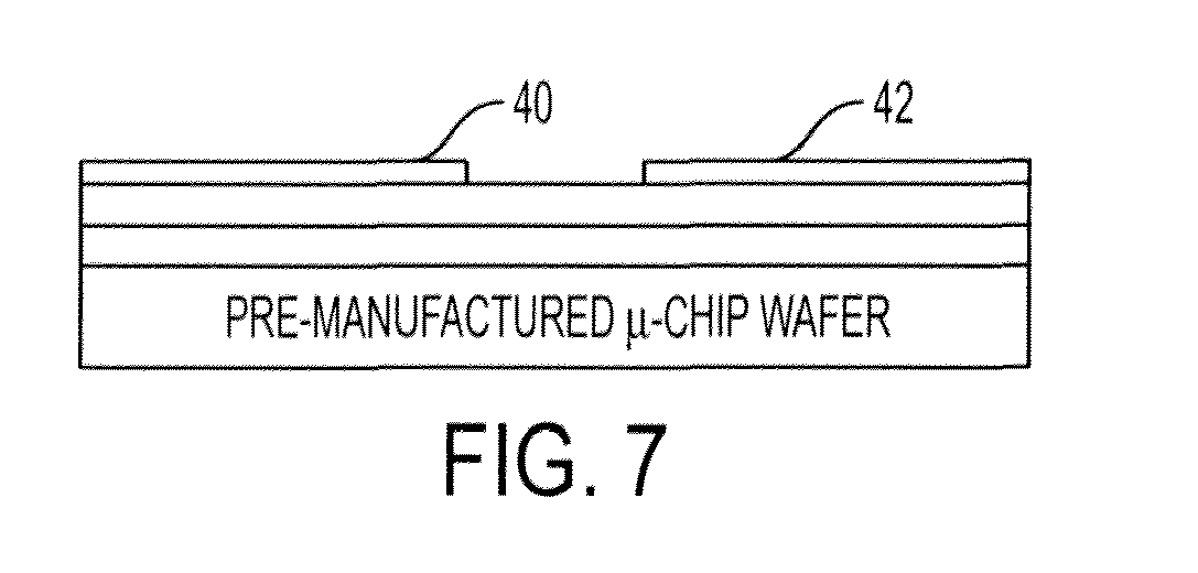
- Figures 4-7 show an embodiment of a method of photolithographically forming charge patterns on a microchip.
- Figures 8-10 show an embodiment of a method of forming a charge pattern using a scorotron.
- Figures 11-13 show an embodiment of a method of forming a bipolar charge template.
- Figure 12-16 show an alternative embodiment of a method of forming a bipolar charge template.
- Figure 1 shows an overall embodiment of a method of forming charge patterns on a microchip.
- the microchips are fabricated on a substrate, such as silicon, gallium arsenide, complementary metal oxide semiconductor (CMOS) etc.
- CMOS complementary metal oxide semiconductor
- the process then deposits materials on the microchips to enable charging at 13.
- the microchips are then submersed in a fluid that causes charge to develop on the materials deposited.
- the materials on the microchips are charged using an external device. The end result is microchips with charge patterns on their surfaces in 19.
- Figure 2 shows an embodiment of a method of forming charge patterns on a microchip.
- the process will more than likely begin at the wafer level at 10, after manufacture of the individual microchips on the wafer. This allows the process of charge patterning to occur in a more mass-produced manner, using techniques compatible with chip fabrication processes. However, no limitation is intended by this discussion and none should be implied.
- the individual chips can be patterned using the same techniques after singulation from the wafer.
- the manufactured microchip 12 has a shield 14 to protect the circuitry on the chip.
- the shield has an insulator 16.
- the insulator allows charge or material patterns deposited on the surface to avoid interaction with the circuitry on the microchip.
- the pattern ABBAB may represent different charges, such as + --+ -, or a pattern of materials into which charge will be developed.
- the charge pattern may consist of alternating regions of differing charge magnitude and/or polarity. The embodiment in this portion of the discussion has the patterns being charge.
- the microchips can be placed into a fluid to create an ⁇ ink' bottle 22 or other dispenser.
- the fluid may contain other additives such as a charge control agent.
- the charge control agent may either allow the charge to remain stable on the surface of the chips 12, or may cause the charge to develop on the surface of the wafer.
- the charge generation may take the form of depositing a material, and developing a charge in the material thorough the interaction of the charge patterning material with the fluid component of the ink.
- One approach uses deposition of a thin-film of the charge patterning material using solution processing techniques such as spin-coating, printing, dip-coating or self-assembly, or vapor deposition techniques such as plasma enhanced chemical vapor deposition (PECVD) or atomic layer deposition (ALD), followed by immersion in solution after deposition of the film.
- solution processing techniques such as spin-coating, printing, dip-coating or self-assembly
- vapor deposition techniques such as plasma enhanced chemical vapor deposition (PECVD) or atomic layer deposition (ALD)
- PECVD plasma enhanced chemical vapor deposition
- ALD atomic layer deposition
- materials that could be deposited by solution or vapor techniques include polymers such as polyethylene, polystyrene, polymethylmethacrylate, and parylene and polyvinylalcohol, as well as cationic and anionic polyelectrolytes such as polystyrenesulfonic acid, polyallylamine, polyacrylic acid, and poly(dial
- organometallic salts such as zinc stearate or aluminum stearate as well as oxides, such as silica, alumina or titania.
- oxides such as silica, alumina or titania.
- materials which form self-assembled monolayers such as octadecyltrichlorosilane, phenethyltrichlorosilane, hexamethyldisilazane, allyltrimethoxysilane or perfluorooctyltrichlorosilane may also be used.
- the charge patterning material may not be a pure material but rather a blend of one or more materials, possibly to enhance charge generating properties, improve processing performance, or impart new functionality to the film such as making it light sensitive.
- materials deposited from solution they would likely be first dissolved in a solvent such as toluene, hexane, water, isopropanol, or tetrahydrofuran to enable solution processing.
- An example process may involve spin coating the material onto the surface of the microchip, patterning the material either using light directly if a light-sensitive formulation of the charge-patterning material is used, or in a separate step through photolithographic/etching cycles, and immersing the chip into solution where free charges are formed through interaction between the fluid and the material.
- a first polymer is spun onto the insulator 16 and photolithographically defined in Figure 5 , exposing a portion of the insulator 16.
- a second polymer 42 is then spun on or otherwise deposited on the first polymer and the exposed insulator in Figure 6 .
- the second polymer is then patterned to define a region separate from the first region, typically with a region of the insulator.
- the two different polymers then retain different charges, or magnitudes of charge to form a charge pattern.
- Typical functional groups that develop a negative surface change include sulfonic acids, phosphonic acids, and carboxylic acids amongst others.
- Typical functional groups that develop positive surface charges include amines and imidazoles, amongst others.
- the range of Coulomb interaction of the charged microchips is controlled by the ionic strength of the solution, but is typically rather short, in the range of 1 to 10 micrometers due to the high ion content.
- non-polar fluids In this embodiment the use of non-polar fluids is desired however, since such Coulomb interactions between charged entities are felt over much larger length scales, in the range of 10-100 micrometers.
- non-polar fluids include isoparaffinic liquids such as the isopar series of fluids, and other hydrocarbon liquids such as dodecane.
- charge control agents typically amphiphilic surfactant materials (both ionic and nonionic), such as phosphatidylcholine (lecithin), sorbitan monooeleate (span-80), aluminium-di-tert-butyl salicylate (ALOHOS), polyisobutylene succinimide (OLOA), or sodium dioctylsulfosuccinate (AOT) amongst others may need to be added to the liquid to assist in developing charge.
- amphiphilic surfactant materials such as phosphatidylcholine (lecithin), sorbitan monooeleate (span-80), aluminium-di-tert-butyl salicylate (ALOHOS), polyisobutylene succinimide (OLOA), or sodium dioctylsulfosuccinate (AOT) amongst others may need to be added to the liquid to assist in developing charge.
- charging of the surface can be done through tribo-actions.
- the toner particles are charged by contacting specifically designed developer particles.
- the charge patterning material has to be selected such that it charges in specific ways when contacted with the developer material.
- the density of the chips should stay low enough to control charge exchange between microchips accidentally hitting each other.
- an ink-jet head 30 can deposit the charge-patterning material.
- Candidate material may include waxes, polymers, such as polyelectrolytes, or blends of materials amongst others. After deposition of the charge patterning material, as in previous descriptions the chips would be singulated and immersed in a fluid where free charges would be generated.
- a self-assembled monolayer can be used along with another material, such as an oxide, to create charged regions on the chip. This could be accomplished, for example, by first depositing the oxide, then depositing the self-assembled monolayer having the desired functionality over the oxide. Using photolithography and etching this self-assembled monolayer could then be patterned revealing the oxide underneath.
- the oxide could be deposited followed be patterning of a sacrificial blocking material (such as photoresist), deposition of the self-assembled monolayer could then take place, followed by removal of the sacrificial material, again revealing the underlying oxide surface, creating an oxide, self-assembled monolayer pattern.
- This second approach has the benefit in that the self-assembled monolayer deposition and blocking material removal steps can be carried out either at the wafer scale, or at the chiplet scale after wafer singulation.
- Figures 4-7 show processes of an embodiment in which photolithographic patterned polymers, inorganic materials or a mixture of the two are used. These materials can either be tribo-charged or chemically charged using a charge control agent, in a dielectric fluid to carry different polarities of charge. Photolithographic defined charging of a dielectric with a corona device is another approach, using dry film resist. Commercially available dry film resists express substantial conductivity difference between exposed ultraviolet and unexposed regions. Figures 4-7 show a process for photolithographic materials.
- a photoconductor coating In a photoconductor coating embodiment, one may use inorganic photoconductor materials such as amorphous silicon and selenium, or single layer or multilayer organic photoconductors. If such a photoconductor coating is used, it receives charge from a corotron or scorotron to give the desired charge signs and patterns.
- a corotron is a corona charging device typically used in electrophotography/Xerography that has a wire connected to a high voltage power source. In a typical application, the wire generates an electric field that charges up a photoreceptor in preparation for receiving charged toner particles.
- a scorotron is a screen corotron.
- FIG. 8 Another embodiment uses photolithographic define charging of a dielectric with a corona device.
- Commercially available dry film resist expresses substantially conductivity difference between ultraviolet exposed and unexposed regions.
- Figures 8-10 show one embodiment of such a process.
- a dry film resist is laminated onto the insulator layer 16 over the microchip or microchip wafer 12.
- ultraviolet light exposes a portion 52 of the dry resist, creating high and low conductivity regions.
- the wafer or microchip 12 is grounded by connection 54 and charged with a scorotron or corotron 56, to form charge patterns based upon the previously exposed regions 50 and 52 of the dry film resist.
- This forms a single charge template, where the surface has one polarity of charge.
- One may verify the charge patterns by spreading beads of known charge and imaging with a camera, or measuring the field directly in air with a non-contact electrostatic volt meter.
- FIGS 11-13 show an embodiment of a method of forming a dual charge template.
- Ultraviolet light exposes a portion of the dry film resist 50 to form a low conductivity region 52.
- Using a stencil mask 62 on top of the dry film resist allows exposure of only a portion of the low conductivity region formed by the UV exposure.
- the scorotron 64 applies charge of a first polarity to a portion of the low conductivity region not protected by the mask 62. The process shifts the mask 62 to cover the charged portion of the low conductivity region.
- the scorotron then charges the uncharged portion of the low conductivity region with a lower dose of the opposite sign ions to create the other sign charge pattern.
- the opposite sign charge pass of the scorotron is referred to as 66.
- a bipolar or a dual charge template can result from a dual exposure, shown in Figures 14-16.
- Figure 14 shows a first exposure forming a first low conductivity region 52 on the dry film resist 50. This first region then receives a first polarity charge from a scorotron 62.
- the dry film resist then receives a second exposure of UV light to form a second low conductivity region 70. This second region then receives a charge of the opposite polarity from the scorotron 64.
- charge patterns can be generated on the surface of microchips, either before or after singulation from a wafer.
- the techniques used are compatible with semiconductor fabrication processes, either using scorotron or corotron charging, tribo-charging, or by application of charged materials. Free charges may then be generated directly or through the interaction of these materials with the surrounding fluid in the chip "ink.”
- the charge patterns contain information usable in automated systems to sort, organize and arrange microchips into larger circuits.
Landscapes
- Physics & Mathematics (AREA)
- General Physics & Mathematics (AREA)
- Application Of Or Painting With Fluid Materials (AREA)
- Manufacturing Of Printed Wiring (AREA)
- Exposure Of Semiconductors, Excluding Electron Or Ion Beam Exposure (AREA)
- Internal Circuitry In Semiconductor Integrated Circuit Devices (AREA)
- Wire Bonding (AREA)
Abstract


Description
- Systems exist that assemble microchips automatically based upon some sort of encoding such as electrostatic or magnetic coding. The system uses the encoding to identify and position the microchips as part of the assembly process.
- Examples of these systems can be found in
US Patent 7,861,405 , and its related cases,US Patent Publications 20100192365 ,20100186221 , and20100186222 , owned by the assignee of this application. Another example is shown inUS Patent 7,332,361 , that teaches charge-encoded elements having basic or acidic surfaces capable of carrying charge in non-polar liquids with charge control agents. Examples include two-particle electrophoretic ink, liquid toner, inorganic oxides and polymers. Standard photolithography or ink-jet technology can be used to pattern these materials to form charge-encoded elements. All of these references are incorporated by reference here. The system uses a charge or magnetic polarity on the chip to sort and position the microchips. - These references make general mention of possible methods of how chips have the charge or polarity, but give no details. For example, issues can arise with the deposition of the charge or polarity. Currently, no current technique exists to deposit a charge pattern on isolated microchips. One approach has charged one end of a nanowire, another has charged up one side of a symmetric microchip, but no work appears to be done on isolated microchips or charge patterning.
- The fabrication process should be compatible with existing devices on the chips. In addition, the process should not increase the manufacturing costs, but still allow the patterning on a scalable level between larger areas and small features. In order to provide a flexible system, the system should allow for varying magnitudes of charge density, and ideally but not necessarily, both positive and negative polarity, for multiple levels of chip control and identification. The charge patterns should have good stability to allow long shelf life of the patterned devices.
- Another issue with patterning may arise with the chips being attracted to each other. They may gather together or conglomerate based upon their respective charges. The density of the chips needs to remain low enough the chips do not exchange charge by contact with each other.
-
Figure 1 show an embodiment of an overall method of forming charge patterns on microchips. -
Figure 2 shows an embodiment of a method of forming charge patterns on a microchip. -
Figure 3 shows an embodiment of a method of printing charge patterns on a microchip. -
Figures 4-7 show an embodiment of a method of photolithographically forming charge patterns on a microchip. -
Figures 8-10 show an embodiment of a method of forming a charge pattern using a scorotron. -
Figures 11-13 show an embodiment of a method of forming a bipolar charge template. -
Figure 12-16 show an alternative embodiment of a method of forming a bipolar charge template. -
Figure 1 shows an overall embodiment of a method of forming charge patterns on a microchip. At 11, the microchips are fabricated on a substrate, such as silicon, gallium arsenide, complementary metal oxide semiconductor (CMOS) etc. The process then deposits materials on the microchips to enable charging at 13. In one approach, shown in more detail inFigures 2-7 , the microchips are then submersed in a fluid that causes charge to develop on the materials deposited. In another approach, shown in more detail inFigures 8-16 , the materials on the microchips are charged using an external device. The end result is microchips with charge patterns on their surfaces in 19. -
Figure 2 shows an embodiment of a method of forming charge patterns on a microchip. The process will more than likely begin at the wafer level at 10, after manufacture of the individual microchips on the wafer. This allows the process of charge patterning to occur in a more mass-produced manner, using techniques compatible with chip fabrication processes. However, no limitation is intended by this discussion and none should be implied. The individual chips can be patterned using the same techniques after singulation from the wafer. - Using manufacturing techniques compatible with chip processing, the manufactured
microchip 12 has ashield 14 to protect the circuitry on the chip. The shield has aninsulator 16. The insulator allows charge or material patterns deposited on the surface to avoid interaction with the circuitry on the microchip. The pattern ABBAB may represent different charges, such as + --+ -, or a pattern of materials into which charge will be developed. Through the techniques discussed in more detail further, the charge pattern may consist of alternating regions of differing charge magnitude and/or polarity. The embodiment in this portion of the discussion has the patterns being charge. - Once singulated, the microchips can be placed into a fluid to create an `ink'
bottle 22 or other dispenser. The fluid may contain other additives such as a charge control agent. The charge control agent may either allow the charge to remain stable on the surface of thechips 12, or may cause the charge to develop on the surface of the wafer. The charge generation may take the form of depositing a material, and developing a charge in the material thorough the interaction of the charge patterning material with the fluid component of the ink. - One approach uses deposition of a thin-film of the charge patterning material using solution processing techniques such as spin-coating, printing, dip-coating or self-assembly, or vapor deposition techniques such as plasma enhanced chemical vapor deposition (PECVD) or atomic layer deposition (ALD), followed by immersion in solution after deposition of the film. Examples of materials that could be deposited by solution or vapor techniques include polymers such as polyethylene, polystyrene, polymethylmethacrylate, and parylene and polyvinylalcohol, as well as cationic and anionic polyelectrolytes such as polystyrenesulfonic acid, polyallylamine, polyacrylic acid, and poly(diallyldimethylammonium chloride). Other examples include organometallic salts such as zinc stearate or aluminum stearate as well as oxides, such as silica, alumina or titania. In addition materials which form self-assembled monolayers such as octadecyltrichlorosilane, phenethyltrichlorosilane, hexamethyldisilazane, allyltrimethoxysilane or perfluorooctyltrichlorosilane may also be used.
- The charge patterning material may not be a pure material but rather a blend of one or more materials, possibly to enhance charge generating properties, improve processing performance, or impart new functionality to the film such as making it light sensitive. For materials deposited from solution, they would likely be first dissolved in a solvent such as toluene, hexane, water, isopropanol, or tetrahydrofuran to enable solution processing. An example process may involve spin coating the material onto the surface of the microchip, patterning the material either using light directly if a light-sensitive formulation of the charge-patterning material is used, or in a separate step through photolithographic/etching cycles, and immersing the chip into solution where free charges are formed through interaction between the fluid and the material.
- In
Figure 4 , a first polymer is spun onto theinsulator 16 and photolithographically defined inFigure 5 , exposing a portion of theinsulator 16. Asecond polymer 42 is then spun on or otherwise deposited on the first polymer and the exposed insulator inFigure 6 . The second polymer is then patterned to define a region separate from the first region, typically with a region of the insulator. The two different polymers then retain different charges, or magnitudes of charge to form a charge pattern. In addition to the use of two solution processed polymers, other embodiments may use a combination of a solution processed material to generate one polarity/magnitude of charge and a vapor deposited material to generate another polarity/magnitude of charge, other embodiments could use two different vapor deposited materials. - If immersed in a polar liquid, such as water, most surfaces become charged, as some of the surface molecules dissociate. Charge tends to be more negative or positive depending on the chemical composition of the surface. Typical functional groups that develop a negative surface change include sulfonic acids, phosphonic acids, and carboxylic acids amongst others. Typical functional groups that develop positive surface charges include amines and imidazoles, amongst others. The range of Coulomb interaction of the charged microchips is controlled by the ionic strength of the solution, but is typically rather short, in the range of 1 to 10 micrometers due to the high ion content.
- In this embodiment the use of non-polar fluids is desired however, since such Coulomb interactions between charged entities are felt over much larger length scales, in the range of 10-100 micrometers. Examples of non-polar fluids include isoparaffinic liquids such as the isopar series of fluids, and other hydrocarbon liquids such as dodecane. In non-polar liquids charge control agents, typically amphiphilic surfactant materials (both ionic and nonionic), such as phosphatidylcholine (lecithin), sorbitan monooeleate (span-80), aluminium-di-tert-butyl salicylate (ALOHOS), polyisobutylene succinimide (OLOA), or sodium dioctylsulfosuccinate (AOT) amongst others may need to be added to the liquid to assist in developing charge.
- If the surrounding liquid is air, charging of the surface can be done through tribo-actions. For example, in Xerography, the toner particles are charged by contacting specifically designed developer particles. The charge patterning material has to be selected such that it charges in specific ways when contacted with the developer material. The density of the chips should stay low enough to control charge exchange between microchips accidentally hitting each other.
- In another approach, shown in
Figure 3 , an ink-jet head 30 can deposit the charge-patterning material. Candidate material may include waxes, polymers, such as polyelectrolytes, or blends of materials amongst others. After deposition of the charge patterning material, as in previous descriptions the chips would be singulated and immersed in a fluid where free charges would be generated. - In another approach, a self-assembled monolayer can be used along with another material, such as an oxide, to create charged regions on the chip. This could be accomplished, for example, by first depositing the oxide, then depositing the self-assembled monolayer having the desired functionality over the oxide. Using photolithography and etching this self-assembled monolayer could then be patterned revealing the oxide underneath. In another approach, the oxide could be deposited followed be patterning of a sacrificial blocking material (such as photoresist), deposition of the self-assembled monolayer could then take place, followed by removal of the sacrificial material, again revealing the underlying oxide surface, creating an oxide, self-assembled monolayer pattern. This second approach has the benefit in that the self-assembled monolayer deposition and blocking material removal steps can be carried out either at the wafer scale, or at the chiplet scale after wafer singulation.
-
Figures 4-7 show processes of an embodiment in which photolithographic patterned polymers, inorganic materials or a mixture of the two are used. These materials can either be tribo-charged or chemically charged using a charge control agent, in a dielectric fluid to carry different polarities of charge. Photolithographic defined charging of a dielectric with a corona device is another approach, using dry film resist. Commercially available dry film resists express substantial conductivity difference between exposed ultraviolet and unexposed regions.Figures 4-7 show a process for photolithographic materials. - In a photoconductor coating embodiment, one may use inorganic photoconductor materials such as amorphous silicon and selenium, or single layer or multilayer organic photoconductors. If such a photoconductor coating is used, it receives charge from a corotron or scorotron to give the desired charge signs and patterns. As the terms are used here, a corotron is a corona charging device typically used in electrophotography/Xerography that has a wire connected to a high voltage power source. In a typical application, the wire generates an electric field that charges up a photoreceptor in preparation for receiving charged toner particles. A scorotron is a screen corotron.
- Another embodiment uses photolithographic define charging of a dielectric with a corona device. Commercially available dry film resist expresses substantially conductivity difference between ultraviolet exposed and unexposed regions.
Figures 8-10 show one embodiment of such a process. InFigure 8 , a dry film resist is laminated onto theinsulator layer 16 over the microchip ormicrochip wafer 12. InFigure 9 , ultraviolet light exposes aportion 52 of the dry resist, creating high and low conductivity regions. InFigure 10 , the wafer ormicrochip 12 is grounded byconnection 54 and charged with a scorotron orcorotron 56, to form charge patterns based upon the previously exposedregions -
Figures 11-13 show an embodiment of a method of forming a dual charge template. Ultraviolet light exposes a portion of the dry film resist 50 to form alow conductivity region 52. Using astencil mask 62 on top of the dry film resist allows exposure of only a portion of the low conductivity region formed by the UV exposure. Thescorotron 64 applies charge of a first polarity to a portion of the low conductivity region not protected by themask 62. The process shifts themask 62 to cover the charged portion of the low conductivity region. The scorotron then charges the uncharged portion of the low conductivity region with a lower dose of the opposite sign ions to create the other sign charge pattern. In order to differentiate between the two scorotron processes, the opposite sign charge pass of the scorotron is referred to as 66. - In an alternative embodiment, a bipolar or a dual charge template can result from a dual exposure, shown in
Figures 14-16. Figure 14 shows a first exposure forming a firstlow conductivity region 52 on the dry film resist 50. This first region then receives a first polarity charge from ascorotron 62. The dry film resist then receives a second exposure of UV light to form a secondlow conductivity region 70. This second region then receives a charge of the opposite polarity from thescorotron 64. - In this manner, charge patterns can be generated on the surface of microchips, either before or after singulation from a wafer. The techniques used are compatible with semiconductor fabrication processes, either using scorotron or corotron charging, tribo-charging, or by application of charged materials. Free charges may then be generated directly or through the interaction of these materials with the surrounding fluid in the chip "ink." The charge patterns contain information usable in automated systems to sort, organize and arrange microchips into larger circuits.
- It will be appreciated that several of the above-disclosed and other features and functions, or alternatives thereof, may be desirably combined into many other different systems or applications. Also that various presently unforeseen or unanticipated alternatives, modifications, variations, or improvements therein may be subsequently made by those skilled in the art which are also intended to be encompassed by the following claims.
- It will be understood that features disclosed in association with particular embodiments are intended to be used with other embodiments unless it would be impractical to do so.
Claims (9)
- A method of forming a charge pattern on a microchip, comprising:depositing a material on the surface of the microchip; andusing an external device to develop charge in the material.
- The method of claim 1, wherein using an external device to develop the charge comprises charging the material with one of either a corotron or a scorotron.
- The method of claim 1 or claim 2, wherein depositing the material comprises depositing a photoconductor.
- The method of claim 1 or claim 2, wherein depositing the material comprises laminating a dry film photoresist onto a wafer and exposing the dry film photoresist to ultraviolet light, and developing the charge comprises charging the exposed photoresist with a scorotron.
- The method of claim 4, wherein exposing the dry film comprises applying a stencil mask to the dry film resist to expose a portion of a low conductivity region and applying a first charge with a scorotron.
- The method of claim 4 or claim 5, further comprising re-exposing the dry film resist with a second charge with a scorotron.
- The method of any of the preceding claims, further comprising singulating the wafer into microchips after charging.
- The method of any of the preceding claims, wherein the depositing of the material comprises depositing one of a polymer, an inorganic material or a mixture of an inorganic and a polymer.
- The method of claim 8, wherein developing the charge comprises tribo-charging.
Applications Claiming Priority (1)
| Application Number | Priority Date | Filing Date | Title |
|---|---|---|---|
| US13/652,220 US8685769B1 (en) | 2012-10-15 | 2012-10-15 | Microchip charge patterning |
Publications (2)
| Publication Number | Publication Date |
|---|---|
| EP2720260A1 true EP2720260A1 (en) | 2014-04-16 |
| EP2720260B1 EP2720260B1 (en) | 2019-07-31 |
Family
ID=49328425
Family Applications (1)
| Application Number | Title | Priority Date | Filing Date |
|---|---|---|---|
| EP13188458.7A Active EP2720260B1 (en) | 2012-10-15 | 2013-10-14 | Microchip charge patterning |
Country Status (3)
| Country | Link |
|---|---|
| US (1) | US8685769B1 (en) |
| EP (1) | EP2720260B1 (en) |
| JP (1) | JP6279870B2 (en) |
Families Citing this family (1)
| Publication number | Priority date | Publication date | Assignee | Title |
|---|---|---|---|---|
| US10141285B2 (en) * | 2013-09-19 | 2018-11-27 | Palo Alto Research Center Incorporated | Externally induced charge patterning using rectifying devices |
Citations (5)
| Publication number | Priority date | Publication date | Assignee | Title |
|---|---|---|---|---|
| US6710436B1 (en) * | 2002-12-12 | 2004-03-23 | Sun Microsystems, Inc. | Method and apparatus for electrostatically aligning integrated circuits |
| WO2006138263A2 (en) * | 2005-06-13 | 2006-12-28 | Electrox Corporation | System and method for the manipulation, classification sorting, purification, placement, and alignment of nano fibers using electrostatic forces and electrographic techniques |
| US7332361B2 (en) | 2004-12-14 | 2008-02-19 | Palo Alto Research Center Incorporated | Xerographic micro-assembler |
| WO2010034824A2 (en) * | 2008-09-26 | 2010-04-01 | Imec | Method for performing parallel stochastic assembly |
| US20100186221A1 (en) | 2008-03-03 | 2010-07-29 | Palo Alto Research Center, Incorporated | Micro-assembler |
Family Cites Families (8)
| Publication number | Priority date | Publication date | Assignee | Title |
|---|---|---|---|---|
| AU607347B2 (en) * | 1988-11-15 | 1991-02-28 | Olin Hunt Specialty Products Inc. | Method of high resolution electrostatic transfer of a high density image to a nonconductive receiving substrate |
| EP1297387A2 (en) * | 2000-06-30 | 2003-04-02 | President And Fellows of Harvard College | Electric microcontact printing method and apparatus |
| JP4175531B2 (en) * | 2000-11-13 | 2008-11-05 | 株式会社リコー | Charger |
| US6825970B2 (en) * | 2001-09-14 | 2004-11-30 | E Ink Corporation | Methods for addressing electro-optic materials |
| US7843621B2 (en) * | 2002-06-10 | 2010-11-30 | E Ink Corporation | Components and testing methods for use in the production of electro-optic displays |
| JP3967202B2 (en) * | 2002-06-11 | 2007-08-29 | 株式会社タムラ製作所 | Method for forming protruding electrode |
| JP2012085515A (en) * | 2010-09-16 | 2012-04-26 | Murata Mfg Co Ltd | Charging device of electret, charging method of electret, and vibration power generating device |
| US10014261B2 (en) * | 2012-10-15 | 2018-07-03 | Palo Alto Research Center Incorporated | Microchip charge patterning |
-
2012
- 2012-10-15 US US13/652,220 patent/US8685769B1/en active Active
-
2013
- 2013-10-01 JP JP2013206542A patent/JP6279870B2/en active Active
- 2013-10-14 EP EP13188458.7A patent/EP2720260B1/en active Active
Patent Citations (8)
| Publication number | Priority date | Publication date | Assignee | Title |
|---|---|---|---|---|
| US6710436B1 (en) * | 2002-12-12 | 2004-03-23 | Sun Microsystems, Inc. | Method and apparatus for electrostatically aligning integrated circuits |
| US7332361B2 (en) | 2004-12-14 | 2008-02-19 | Palo Alto Research Center Incorporated | Xerographic micro-assembler |
| WO2006138263A2 (en) * | 2005-06-13 | 2006-12-28 | Electrox Corporation | System and method for the manipulation, classification sorting, purification, placement, and alignment of nano fibers using electrostatic forces and electrographic techniques |
| US20100186221A1 (en) | 2008-03-03 | 2010-07-29 | Palo Alto Research Center, Incorporated | Micro-assembler |
| US20100186222A1 (en) | 2008-03-03 | 2010-07-29 | Palo Alto Research Center, Incorporated | Micro-assembler |
| US20100192365A1 (en) | 2008-03-03 | 2010-08-05 | Palo Alto Research Center, Incorporated | Micro-assembler |
| US7861405B2 (en) | 2008-03-03 | 2011-01-04 | Palo Alto Research Center Incorporated | System for forming a micro-assembler |
| WO2010034824A2 (en) * | 2008-09-26 | 2010-04-01 | Imec | Method for performing parallel stochastic assembly |
Non-Patent Citations (1)
| Title |
|---|
| HUANG C ET AL: "ORGANIC FIELD-EFFECT TRANSISTORS AND UNIPOLAR LOGIC GATES ON CHARGED ELECTRETS FROM SPIN-ON ORGANOSILSESQUIOXANE RESINS", ADVANCED FUNCTIONAL MATERIALS, WILEY - V C H VERLAG GMBH & CO. KGAA, DE, vol. 17, no. 1, 5 January 2007 (2007-01-05), pages 142 - 153, XP001504246, ISSN: 1616-301X, DOI: 10.1002/ADFM.200600690 * |
Also Published As
| Publication number | Publication date |
|---|---|
| US8685769B1 (en) | 2014-04-01 |
| EP2720260B1 (en) | 2019-07-31 |
| US20140106512A1 (en) | 2014-04-17 |
| JP6279870B2 (en) | 2018-02-14 |
| JP2014082491A (en) | 2014-05-08 |
Similar Documents
| Publication | Publication Date | Title |
|---|---|---|
| US20230187373A1 (en) | Microchip charge patterning | |
| McCarty et al. | Ionic electrets: electrostatic charging of surfaces by transferring mobile ions upon contact | |
| JP6678234B2 (en) | Graphene-based magnetic Hall sensor for fluid flow analysis at the nanoscale level | |
| Jeong et al. | Electrical biomolecule detection using nanopatterned silicon via block copolymer lithography | |
| BR112015029548B1 (en) | MANUFACTURING METHOD AND INTEGRATED CIRCUIT SUBSTRATE | |
| US9761620B1 (en) | Method and system for manufacturing using a programmable patterning structure | |
| US20150076961A1 (en) | Method for reduction of stiction while manipulating micro objects on a surface | |
| KR20080104947A (en) | A method for focusing patterning of charged particles using a patterned perforated mask and a mask used therein | |
| EP2720260B1 (en) | Microchip charge patterning | |
| Cole et al. | Nanocontact electrification: patterned surface charges affecting adhesion, transfer, and printing | |
| EP2851338A2 (en) | Externally induced charge patterning using rectifying devices for assembling micro-objects | |
| Cole et al. | Nanocontact electrification through forced delamination of dielectric interfaces | |
| KR102198983B1 (en) | Method for manufacturing pattern-formed body | |
| KR20070051004A (en) | Stamp manufacturing method, thin film transistor and liquid crystal display device manufacturing method using the same | |
| Truman et al. | A stack of functional nanolayers for simultaneous emulsion separation and sensing | |
| EP1424602A3 (en) | Photoreceptor for electrophotography having an overcoat layer with salt | |
| Schnupp et al. | Electrodeposition of photoresist: optimization of deposition conditions, investigation of lithographic processes and chemical resistance | |
| Dickey et al. | Transistors formed from a single lithography step using information encoded in topography | |
| JP5068950B2 (en) | Toner and image forming method using the same | |
| Smallwood | Electrochemical materials for integrated magnetics | |
| JP4327133B2 (en) | Electronic circuit manufacturing method | |
| US8304150B1 (en) | Electrostatic printing of functional toner materials for the construction of useful micro-structures | |
| JP6714924B2 (en) | Sample detection device, sample detection device, and ion current detection method | |
| US10308504B2 (en) | Hierarchical micro assembler system | |
| SU409450A1 (en) | METHOD OF FORMING ELECTROSTATIC IMAGE |
Legal Events
| Date | Code | Title | Description |
|---|---|---|---|
| PUAI | Public reference made under article 153(3) epc to a published international application that has entered the european phase |
Free format text: ORIGINAL CODE: 0009012 |
|
| AK | Designated contracting states |
Kind code of ref document: A1 Designated state(s): AL AT BE BG CH CY CZ DE DK EE ES FI FR GB GR HR HU IE IS IT LI LT LU LV MC MK MT NL NO PL PT RO RS SE SI SK SM TR |
|
| AX | Request for extension of the european patent |
Extension state: BA ME |
|
| 17P | Request for examination filed |
Effective date: 20141016 |
|
| RBV | Designated contracting states (corrected) |
Designated state(s): AL AT BE BG CH CY CZ DE DK EE ES FI FR GB GR HR HU IE IS IT LI LT LU LV MC MK MT NL NO PL PT RO RS SE SI SK SM TR |
|
| STAA | Information on the status of an ep patent application or granted ep patent |
Free format text: STATUS: EXAMINATION IS IN PROGRESS |
|
| 17Q | First examination report despatched |
Effective date: 20180503 |
|
| GRAP | Despatch of communication of intention to grant a patent |
Free format text: ORIGINAL CODE: EPIDOSNIGR1 |
|
| STAA | Information on the status of an ep patent application or granted ep patent |
Free format text: STATUS: GRANT OF PATENT IS INTENDED |
|
| INTG | Intention to grant announced |
Effective date: 20190226 |
|
| GRAS | Grant fee paid |
Free format text: ORIGINAL CODE: EPIDOSNIGR3 |
|
| GRAA | (expected) grant |
Free format text: ORIGINAL CODE: 0009210 |
|
| STAA | Information on the status of an ep patent application or granted ep patent |
Free format text: STATUS: THE PATENT HAS BEEN GRANTED |
|
| AK | Designated contracting states |
Kind code of ref document: B1 Designated state(s): AL AT BE BG CH CY CZ DE DK EE ES FI FR GB GR HR HU IE IS IT LI LT LU LV MC MK MT NL NO PL PT RO RS SE SI SK SM TR |
|
| REG | Reference to a national code |
Ref country code: CH Ref legal event code: EP Ref country code: GB Ref legal event code: FG4D |
|
| REG | Reference to a national code |
Ref country code: AT Ref legal event code: REF Ref document number: 1161830 Country of ref document: AT Kind code of ref document: T Effective date: 20190815 |
|
| REG | Reference to a national code |
Ref country code: IE Ref legal event code: FG4D |
|
| REG | Reference to a national code |
Ref country code: DE Ref legal event code: R096 Ref document number: 602013058430 Country of ref document: DE |
|
| REG | Reference to a national code |
Ref country code: NL Ref legal event code: MP Effective date: 20190731 |
|
| REG | Reference to a national code |
Ref country code: LT Ref legal event code: MG4D |
|
| REG | Reference to a national code |
Ref country code: AT Ref legal event code: MK05 Ref document number: 1161830 Country of ref document: AT Kind code of ref document: T Effective date: 20190731 |
|
| PG25 | Lapsed in a contracting state [announced via postgrant information from national office to epo] |
Ref country code: NO Free format text: LAPSE BECAUSE OF FAILURE TO SUBMIT A TRANSLATION OF THE DESCRIPTION OR TO PAY THE FEE WITHIN THE PRESCRIBED TIME-LIMIT Effective date: 20191031 Ref country code: HR Free format text: LAPSE BECAUSE OF FAILURE TO SUBMIT A TRANSLATION OF THE DESCRIPTION OR TO PAY THE FEE WITHIN THE PRESCRIBED TIME-LIMIT Effective date: 20190731 Ref country code: SE Free format text: LAPSE BECAUSE OF FAILURE TO SUBMIT A TRANSLATION OF THE DESCRIPTION OR TO PAY THE FEE WITHIN THE PRESCRIBED TIME-LIMIT Effective date: 20190731 Ref country code: FI Free format text: LAPSE BECAUSE OF FAILURE TO SUBMIT A TRANSLATION OF THE DESCRIPTION OR TO PAY THE FEE WITHIN THE PRESCRIBED TIME-LIMIT Effective date: 20190731 Ref country code: LT Free format text: LAPSE BECAUSE OF FAILURE TO SUBMIT A TRANSLATION OF THE DESCRIPTION OR TO PAY THE FEE WITHIN THE PRESCRIBED TIME-LIMIT Effective date: 20190731 Ref country code: PT Free format text: LAPSE BECAUSE OF FAILURE TO SUBMIT A TRANSLATION OF THE DESCRIPTION OR TO PAY THE FEE WITHIN THE PRESCRIBED TIME-LIMIT Effective date: 20191202 Ref country code: AT Free format text: LAPSE BECAUSE OF FAILURE TO SUBMIT A TRANSLATION OF THE DESCRIPTION OR TO PAY THE FEE WITHIN THE PRESCRIBED TIME-LIMIT Effective date: 20190731 Ref country code: BG Free format text: LAPSE BECAUSE OF FAILURE TO SUBMIT A TRANSLATION OF THE DESCRIPTION OR TO PAY THE FEE WITHIN THE PRESCRIBED TIME-LIMIT Effective date: 20191031 Ref country code: NL Free format text: LAPSE BECAUSE OF FAILURE TO SUBMIT A TRANSLATION OF THE DESCRIPTION OR TO PAY THE FEE WITHIN THE PRESCRIBED TIME-LIMIT Effective date: 20190731 |
|
| PG25 | Lapsed in a contracting state [announced via postgrant information from national office to epo] |
Ref country code: AL Free format text: LAPSE BECAUSE OF FAILURE TO SUBMIT A TRANSLATION OF THE DESCRIPTION OR TO PAY THE FEE WITHIN THE PRESCRIBED TIME-LIMIT Effective date: 20190731 Ref country code: ES Free format text: LAPSE BECAUSE OF FAILURE TO SUBMIT A TRANSLATION OF THE DESCRIPTION OR TO PAY THE FEE WITHIN THE PRESCRIBED TIME-LIMIT Effective date: 20190731 Ref country code: LV Free format text: LAPSE BECAUSE OF FAILURE TO SUBMIT A TRANSLATION OF THE DESCRIPTION OR TO PAY THE FEE WITHIN THE PRESCRIBED TIME-LIMIT Effective date: 20190731 Ref country code: GR Free format text: LAPSE BECAUSE OF FAILURE TO SUBMIT A TRANSLATION OF THE DESCRIPTION OR TO PAY THE FEE WITHIN THE PRESCRIBED TIME-LIMIT Effective date: 20191101 Ref country code: IS Free format text: LAPSE BECAUSE OF FAILURE TO SUBMIT A TRANSLATION OF THE DESCRIPTION OR TO PAY THE FEE WITHIN THE PRESCRIBED TIME-LIMIT Effective date: 20191130 Ref country code: RS Free format text: LAPSE BECAUSE OF FAILURE TO SUBMIT A TRANSLATION OF THE DESCRIPTION OR TO PAY THE FEE WITHIN THE PRESCRIBED TIME-LIMIT Effective date: 20190731 |
|
| PG25 | Lapsed in a contracting state [announced via postgrant information from national office to epo] |
Ref country code: TR Free format text: LAPSE BECAUSE OF FAILURE TO SUBMIT A TRANSLATION OF THE DESCRIPTION OR TO PAY THE FEE WITHIN THE PRESCRIBED TIME-LIMIT Effective date: 20190731 |
|
| PG25 | Lapsed in a contracting state [announced via postgrant information from national office to epo] |
Ref country code: RO Free format text: LAPSE BECAUSE OF FAILURE TO SUBMIT A TRANSLATION OF THE DESCRIPTION OR TO PAY THE FEE WITHIN THE PRESCRIBED TIME-LIMIT Effective date: 20190731 Ref country code: EE Free format text: LAPSE BECAUSE OF FAILURE TO SUBMIT A TRANSLATION OF THE DESCRIPTION OR TO PAY THE FEE WITHIN THE PRESCRIBED TIME-LIMIT Effective date: 20190731 Ref country code: PL Free format text: LAPSE BECAUSE OF FAILURE TO SUBMIT A TRANSLATION OF THE DESCRIPTION OR TO PAY THE FEE WITHIN THE PRESCRIBED TIME-LIMIT Effective date: 20190731 Ref country code: IT Free format text: LAPSE BECAUSE OF FAILURE TO SUBMIT A TRANSLATION OF THE DESCRIPTION OR TO PAY THE FEE WITHIN THE PRESCRIBED TIME-LIMIT Effective date: 20190731 Ref country code: DK Free format text: LAPSE BECAUSE OF FAILURE TO SUBMIT A TRANSLATION OF THE DESCRIPTION OR TO PAY THE FEE WITHIN THE PRESCRIBED TIME-LIMIT Effective date: 20190731 |
|
| PG25 | Lapsed in a contracting state [announced via postgrant information from national office to epo] |
Ref country code: MC Free format text: LAPSE BECAUSE OF FAILURE TO SUBMIT A TRANSLATION OF THE DESCRIPTION OR TO PAY THE FEE WITHIN THE PRESCRIBED TIME-LIMIT Effective date: 20190731 Ref country code: SM Free format text: LAPSE BECAUSE OF FAILURE TO SUBMIT A TRANSLATION OF THE DESCRIPTION OR TO PAY THE FEE WITHIN THE PRESCRIBED TIME-LIMIT Effective date: 20190731 Ref country code: SK Free format text: LAPSE BECAUSE OF FAILURE TO SUBMIT A TRANSLATION OF THE DESCRIPTION OR TO PAY THE FEE WITHIN THE PRESCRIBED TIME-LIMIT Effective date: 20190731 Ref country code: CZ Free format text: LAPSE BECAUSE OF FAILURE TO SUBMIT A TRANSLATION OF THE DESCRIPTION OR TO PAY THE FEE WITHIN THE PRESCRIBED TIME-LIMIT Effective date: 20190731 Ref country code: IS Free format text: LAPSE BECAUSE OF FAILURE TO SUBMIT A TRANSLATION OF THE DESCRIPTION OR TO PAY THE FEE WITHIN THE PRESCRIBED TIME-LIMIT Effective date: 20200224 |
|
| REG | Reference to a national code |
Ref country code: CH Ref legal event code: PL |
|
| REG | Reference to a national code |
Ref country code: DE Ref legal event code: R097 Ref document number: 602013058430 Country of ref document: DE |
|
| PLBE | No opposition filed within time limit |
Free format text: ORIGINAL CODE: 0009261 |
|
| STAA | Information on the status of an ep patent application or granted ep patent |
Free format text: STATUS: NO OPPOSITION FILED WITHIN TIME LIMIT |
|
| PG2D | Information on lapse in contracting state deleted |
Ref country code: IS |
|
| PG25 | Lapsed in a contracting state [announced via postgrant information from national office to epo] |
Ref country code: LI Free format text: LAPSE BECAUSE OF NON-PAYMENT OF DUE FEES Effective date: 20191031 Ref country code: LU Free format text: LAPSE BECAUSE OF NON-PAYMENT OF DUE FEES Effective date: 20191014 Ref country code: CH Free format text: LAPSE BECAUSE OF NON-PAYMENT OF DUE FEES Effective date: 20191031 Ref country code: IS Free format text: LAPSE BECAUSE OF FAILURE TO SUBMIT A TRANSLATION OF THE DESCRIPTION OR TO PAY THE FEE WITHIN THE PRESCRIBED TIME-LIMIT Effective date: 20191030 |
|
| 26N | No opposition filed |
Effective date: 20200603 |
|
| REG | Reference to a national code |
Ref country code: BE Ref legal event code: MM Effective date: 20191031 |
|
| PG25 | Lapsed in a contracting state [announced via postgrant information from national office to epo] |
Ref country code: SI Free format text: LAPSE BECAUSE OF FAILURE TO SUBMIT A TRANSLATION OF THE DESCRIPTION OR TO PAY THE FEE WITHIN THE PRESCRIBED TIME-LIMIT Effective date: 20190731 Ref country code: BE Free format text: LAPSE BECAUSE OF NON-PAYMENT OF DUE FEES Effective date: 20191031 |
|
| PG25 | Lapsed in a contracting state [announced via postgrant information from national office to epo] |
Ref country code: IE Free format text: LAPSE BECAUSE OF NON-PAYMENT OF DUE FEES Effective date: 20191014 |
|
| PG25 | Lapsed in a contracting state [announced via postgrant information from national office to epo] |
Ref country code: CY Free format text: LAPSE BECAUSE OF FAILURE TO SUBMIT A TRANSLATION OF THE DESCRIPTION OR TO PAY THE FEE WITHIN THE PRESCRIBED TIME-LIMIT Effective date: 20190731 |
|
| PG25 | Lapsed in a contracting state [announced via postgrant information from national office to epo] |
Ref country code: MT Free format text: LAPSE BECAUSE OF FAILURE TO SUBMIT A TRANSLATION OF THE DESCRIPTION OR TO PAY THE FEE WITHIN THE PRESCRIBED TIME-LIMIT Effective date: 20190731 Ref country code: HU Free format text: LAPSE BECAUSE OF FAILURE TO SUBMIT A TRANSLATION OF THE DESCRIPTION OR TO PAY THE FEE WITHIN THE PRESCRIBED TIME-LIMIT; INVALID AB INITIO Effective date: 20131014 |
|
| PG25 | Lapsed in a contracting state [announced via postgrant information from national office to epo] |
Ref country code: MK Free format text: LAPSE BECAUSE OF FAILURE TO SUBMIT A TRANSLATION OF THE DESCRIPTION OR TO PAY THE FEE WITHIN THE PRESCRIBED TIME-LIMIT Effective date: 20190731 |
|
| REG | Reference to a national code |
Ref country code: DE Ref legal event code: R079 Ref document number: 602013058430 Country of ref document: DE Free format text: PREVIOUS MAIN CLASS: H01L0021980000 Ipc: H10W0090240000 |
|
| PGFP | Annual fee paid to national office [announced via postgrant information from national office to epo] |
Ref country code: GB Payment date: 20251219 Year of fee payment: 13 |
|
| PGFP | Annual fee paid to national office [announced via postgrant information from national office to epo] |
Ref country code: FR Payment date: 20251219 Year of fee payment: 13 |
|
| PGFP | Annual fee paid to national office [announced via postgrant information from national office to epo] |
Ref country code: DE Payment date: 20251230 Year of fee payment: 13 |