EP2720257A1 - Semiconductor element, hemt element, and method for manufacturing semiconductor element - Google Patents
Semiconductor element, hemt element, and method for manufacturing semiconductor element Download PDFInfo
- Publication number
- EP2720257A1 EP2720257A1 EP20120842688 EP12842688A EP2720257A1 EP 2720257 A1 EP2720257 A1 EP 2720257A1 EP 20120842688 EP20120842688 EP 20120842688 EP 12842688 A EP12842688 A EP 12842688A EP 2720257 A1 EP2720257 A1 EP 2720257A1
- Authority
- EP
- European Patent Office
- Prior art keywords
- layer
- semiconductor device
- group
- iii nitride
- electrode
- Prior art date
- Legal status (The legal status is an assumption and is not a legal conclusion. Google has not performed a legal analysis and makes no representation as to the accuracy of the status listed.)
- Ceased
Links
Images


Classifications
-
- H—ELECTRICITY
- H10—SEMICONDUCTOR DEVICES; ELECTRIC SOLID-STATE DEVICES NOT OTHERWISE PROVIDED FOR
- H10D—INORGANIC ELECTRIC SEMICONDUCTOR DEVICES
- H10D30/00—Field-effect transistors [FET]
- H10D30/40—FETs having zero-dimensional [0D], one-dimensional [1D] or two-dimensional [2D] charge carrier gas channels
- H10D30/47—FETs having zero-dimensional [0D], one-dimensional [1D] or two-dimensional [2D] charge carrier gas channels having two-dimensional [2D] charge carrier gas channels, e.g. nanoribbon FETs or high electron mobility transistors [HEMT]
-
- H—ELECTRICITY
- H10—SEMICONDUCTOR DEVICES; ELECTRIC SOLID-STATE DEVICES NOT OTHERWISE PROVIDED FOR
- H10D—INORGANIC ELECTRIC SEMICONDUCTOR DEVICES
- H10D30/00—Field-effect transistors [FET]
- H10D30/01—Manufacture or treatment
- H10D30/015—Manufacture or treatment of FETs having heterojunction interface channels or heterojunction gate electrodes, e.g. HEMT
-
- H—ELECTRICITY
- H10—SEMICONDUCTOR DEVICES; ELECTRIC SOLID-STATE DEVICES NOT OTHERWISE PROVIDED FOR
- H10D—INORGANIC ELECTRIC SEMICONDUCTOR DEVICES
- H10D30/00—Field-effect transistors [FET]
- H10D30/40—FETs having zero-dimensional [0D], one-dimensional [1D] or two-dimensional [2D] charge carrier gas channels
- H10D30/47—FETs having zero-dimensional [0D], one-dimensional [1D] or two-dimensional [2D] charge carrier gas channels having two-dimensional [2D] charge carrier gas channels, e.g. nanoribbon FETs or high electron mobility transistors [HEMT]
- H10D30/471—High electron mobility transistors [HEMT] or high hole mobility transistors [HHMT]
- H10D30/475—High electron mobility transistors [HEMT] or high hole mobility transistors [HHMT] having wider bandgap layer formed on top of lower bandgap active layer, e.g. undoped barrier HEMTs such as i-AlGaN/GaN HEMTs
-
- H—ELECTRICITY
- H10—SEMICONDUCTOR DEVICES; ELECTRIC SOLID-STATE DEVICES NOT OTHERWISE PROVIDED FOR
- H10D—INORGANIC ELECTRIC SEMICONDUCTOR DEVICES
- H10D62/00—Semiconductor bodies, or regions thereof, of devices having potential barriers
- H10D62/80—Semiconductor bodies, or regions thereof, of devices having potential barriers characterised by the materials
- H10D62/82—Heterojunctions
- H10D62/824—Heterojunctions comprising only Group III-V materials heterojunctions, e.g. GaN/AlGaN heterojunctions
-
- H—ELECTRICITY
- H10—SEMICONDUCTOR DEVICES; ELECTRIC SOLID-STATE DEVICES NOT OTHERWISE PROVIDED FOR
- H10D—INORGANIC ELECTRIC SEMICONDUCTOR DEVICES
- H10D64/00—Electrodes of devices having potential barriers
- H10D64/60—Electrodes characterised by their materials
- H10D64/602—Heterojunction gate electrodes for FETs
-
- H—ELECTRICITY
- H10—SEMICONDUCTOR DEVICES; ELECTRIC SOLID-STATE DEVICES NOT OTHERWISE PROVIDED FOR
- H10D—INORGANIC ELECTRIC SEMICONDUCTOR DEVICES
- H10D64/00—Electrodes of devices having potential barriers
- H10D64/60—Electrodes characterised by their materials
- H10D64/66—Electrodes having a conductor capacitively coupled to a semiconductor by an insulator, e.g. MIS electrodes
- H10D64/68—Electrodes having a conductor capacitively coupled to a semiconductor by an insulator, e.g. MIS electrodes characterised by the insulator, e.g. by the gate insulator
- H10D64/693—Electrodes having a conductor capacitively coupled to a semiconductor by an insulator, e.g. MIS electrodes characterised by the insulator, e.g. by the gate insulator the insulator comprising nitrogen, e.g. nitrides, oxynitrides or nitrogen-doped materials
-
- H—ELECTRICITY
- H10—SEMICONDUCTOR DEVICES; ELECTRIC SOLID-STATE DEVICES NOT OTHERWISE PROVIDED FOR
- H10P—GENERIC PROCESSES OR APPARATUS FOR THE MANUFACTURE OR TREATMENT OF DEVICES COVERED BY CLASS H10
- H10P14/00—Formation of materials, e.g. in the shape of layers or pillars
- H10P14/20—Formation of materials, e.g. in the shape of layers or pillars of semiconductor materials
- H10P14/24—Formation of materials, e.g. in the shape of layers or pillars of semiconductor materials using chemical vapour deposition [CVD]
-
- H—ELECTRICITY
- H10—SEMICONDUCTOR DEVICES; ELECTRIC SOLID-STATE DEVICES NOT OTHERWISE PROVIDED FOR
- H10P—GENERIC PROCESSES OR APPARATUS FOR THE MANUFACTURE OR TREATMENT OF DEVICES COVERED BY CLASS H10
- H10P14/00—Formation of materials, e.g. in the shape of layers or pillars
- H10P14/20—Formation of materials, e.g. in the shape of layers or pillars of semiconductor materials
- H10P14/29—Formation of materials, e.g. in the shape of layers or pillars of semiconductor materials characterised by the substrates
- H10P14/2901—Materials
- H10P14/2902—Materials being Group IVA materials
- H10P14/2904—Silicon carbide
-
- H—ELECTRICITY
- H10—SEMICONDUCTOR DEVICES; ELECTRIC SOLID-STATE DEVICES NOT OTHERWISE PROVIDED FOR
- H10P—GENERIC PROCESSES OR APPARATUS FOR THE MANUFACTURE OR TREATMENT OF DEVICES COVERED BY CLASS H10
- H10P14/00—Formation of materials, e.g. in the shape of layers or pillars
- H10P14/20—Formation of materials, e.g. in the shape of layers or pillars of semiconductor materials
- H10P14/29—Formation of materials, e.g. in the shape of layers or pillars of semiconductor materials characterised by the substrates
- H10P14/2901—Materials
- H10P14/2902—Materials being Group IVA materials
- H10P14/2905—Silicon, silicon germanium or germanium
-
- H—ELECTRICITY
- H10—SEMICONDUCTOR DEVICES; ELECTRIC SOLID-STATE DEVICES NOT OTHERWISE PROVIDED FOR
- H10P—GENERIC PROCESSES OR APPARATUS FOR THE MANUFACTURE OR TREATMENT OF DEVICES COVERED BY CLASS H10
- H10P14/00—Formation of materials, e.g. in the shape of layers or pillars
- H10P14/20—Formation of materials, e.g. in the shape of layers or pillars of semiconductor materials
- H10P14/32—Formation of materials, e.g. in the shape of layers or pillars of semiconductor materials characterised by intermediate layers between substrates and deposited layers
- H10P14/3202—Materials thereof
- H10P14/3214—Materials thereof being Group IIIA-VA semiconductors
- H10P14/3216—Nitrides
-
- H—ELECTRICITY
- H10—SEMICONDUCTOR DEVICES; ELECTRIC SOLID-STATE DEVICES NOT OTHERWISE PROVIDED FOR
- H10P—GENERIC PROCESSES OR APPARATUS FOR THE MANUFACTURE OR TREATMENT OF DEVICES COVERED BY CLASS H10
- H10P14/00—Formation of materials, e.g. in the shape of layers or pillars
- H10P14/20—Formation of materials, e.g. in the shape of layers or pillars of semiconductor materials
- H10P14/32—Formation of materials, e.g. in the shape of layers or pillars of semiconductor materials characterised by intermediate layers between substrates and deposited layers
- H10P14/3242—Structure
- H10P14/3244—Layer structure
- H10P14/3248—Layer structure consisting of two layers
-
- H—ELECTRICITY
- H10—SEMICONDUCTOR DEVICES; ELECTRIC SOLID-STATE DEVICES NOT OTHERWISE PROVIDED FOR
- H10P—GENERIC PROCESSES OR APPARATUS FOR THE MANUFACTURE OR TREATMENT OF DEVICES COVERED BY CLASS H10
- H10P14/00—Formation of materials, e.g. in the shape of layers or pillars
- H10P14/20—Formation of materials, e.g. in the shape of layers or pillars of semiconductor materials
- H10P14/34—Deposited materials, e.g. layers
- H10P14/3402—Deposited materials, e.g. layers characterised by the chemical composition
- H10P14/3414—Deposited materials, e.g. layers characterised by the chemical composition being group IIIA-VIA materials
- H10P14/3416—Nitrides
-
- H—ELECTRICITY
- H10—SEMICONDUCTOR DEVICES; ELECTRIC SOLID-STATE DEVICES NOT OTHERWISE PROVIDED FOR
- H10P—GENERIC PROCESSES OR APPARATUS FOR THE MANUFACTURE OR TREATMENT OF DEVICES COVERED BY CLASS H10
- H10P14/00—Formation of materials, e.g. in the shape of layers or pillars
- H10P14/60—Formation of materials, e.g. in the shape of layers or pillars of insulating materials
- H10P14/63—Formation of materials, e.g. in the shape of layers or pillars of insulating materials characterised by the formation processes
- H10P14/6326—Deposition processes
- H10P14/6349—Deposition of epitaxial materials
-
- H—ELECTRICITY
- H10—SEMICONDUCTOR DEVICES; ELECTRIC SOLID-STATE DEVICES NOT OTHERWISE PROVIDED FOR
- H10D—INORGANIC ELECTRIC SEMICONDUCTOR DEVICES
- H10D62/00—Semiconductor bodies, or regions thereof, of devices having potential barriers
- H10D62/80—Semiconductor bodies, or regions thereof, of devices having potential barriers characterised by the materials
- H10D62/85—Semiconductor bodies, or regions thereof, of devices having potential barriers characterised by the materials being Group III-V materials, e.g. GaAs
- H10D62/8503—Nitride Group III-V materials, e.g. AlN or GaN
Definitions
- the present invention relates to a semiconductor device, and particularly to a semiconductor device in which a Schottky diode junction is established between an epitaxial substrate having a multilayer structure made of a group-III nitride semiconductor and a metal electrode.
- a group-III nitride semiconductor is attracting attention as a semiconductor material for a next-generation high-frequency/high-power device, because the nitride semiconductor has a high breakdown electric field and a high saturation electron velocity.
- an HEMT (high electron mobility transistor) device in which a barrier layer made of AlGaN and a channel layer made of GaN are laminated takes advantage of the feature that causes a high-concentration two-dimensional electron gas (2DEG) to occur in a lamination interface (hetero interface) due to the large polarization effect (a spontaneous polarization effect and a piezo polarization effect) specific to a nitride material (for example, see Non-Patent Document 1).
- 2DEG high-concentration two-dimensional electron gas
- a single crystal (a different kind single crystal) having a composition different from that of a group-III nitride, such as silicon and SiC is used as a base substrate of an HEMT-device substrate.
- a buffer layer such as a strained-superlattice layer or a low-temperature growth buffer layer is generally formed as an initially-grown layer on the base substrate. Accordingly, a configuration in which a barrier layer, a channel layer, and a buffer layer are epitaxially formed on a base substrate is the most basic configuration of the HEMT-device substrate including a base substrate made of a different kind single crystal.
- a spacer layer having a thickness of about 1 nm may be sometimes provided between the barrier layer and the channel layer, for the purpose of facilitating a spatial confinement of the two-dimensional electron gas.
- the spacer layer is made of, for example, AlN.
- a cap layer made of, for example, an n-type GaN layer or a superlattice layer may be sometimes formed on the barrier layer, for the purpose of controlling the energy level at the most superficial surface of the HEMT-device substrate and improving contact characteristics of contact with an electrode.
- a nitride HEMT device has the most general configuration in which a channel layer is made of GaN and a barrier layer is made of AlGaN
- the concentration of a two-dimensional electron gas existing in an HEMT-device substrate increases as the AlN mole fraction in AlGaN of the barrier layer increases (for example, see Non-Patent Document 2). If the concentration of the two-dimensional electron gas can be considerably increased, the controllable current density of the HEMT device, that is, the power density that can be handled, would be considerably improved.
- an HEMT device having a structure with reduced strain such as an HEMT device in which a channel layer is made of GaN and a barrier layer is made of InAlN, in which the dependence on a piezo polarization effect is small and almost only a spontaneous polarization is used to generate a two-dimensional electron gas with a high concentration (for example, see Non-Patent Document 3).
- a junction formed between a gate electrode and the barrier layer is generally a Schottky junction.
- a large leakage current occurs when a reverse voltage is applied to the Schottky junction.
- Forming a contact layer made of AlN on the InAlN layer can reduce the leakage current.
- an HEMT device having such a configuration involves a problem that the mobility of a two-dimensional electron gas is low. The cause thereof is assumed to be occurrence of strain in the InAlN layer due to the lattice constant of the AlN layer being smaller than that of the InAlN layer.
- Non-Patent Document 1 " Highly Reliable 250W High Electron Mobility Transistor Power Amplifier", TOSHIHIDE KIKKAWA, Jpn. J. Appl. Phys. 44, (2005), 4896
- Non-Patent Document 2 Gallium Nitride Based High Power Heterojunction Field Effect Transistors: process Development and Present Status at USCB", Stacia Keller, Yi-Feng Wu, Giacinta Parish, Naiqian Ziang, Jane J. Xu, Bernd P. Keller, Steven P. DenBaars, and Umesh K. Mishra, IEEE Trans. Electron Devices 48, (2001), 552
- Non-Patent Document 3 " Can InAlN/GaN be an alternative to high power/high temperature AlGaN/GaN devices?", F. Medjdoub, J.-F. Carlin, M. Gonschorek, E. Feltin, M.A. Py, D. Ducatteau, C. Gaquiere, N. Grandjean, and E. Kohn, IEEE IEDM Tech. Digest in IEEE IEDM 2006, 673
- the present invention has been made in view of the problems described above, and an object of the present invention is to provide a semiconductor device in which a reverse leakage current is suppressed and the mobility of a two-dimensional electron gas is high.
- a first aspect of the present invention is a semiconductor device including: an epitaxial substrate in which a group of group-III nitride layers are laminated on a base substrate such that a (0001) crystal plane is substantially in parallel with a substrate surface; and a Schottky electrode.
- the Schottky electrode is bonded to the cap layer.
- a second aspect of the present invention is the semiconductor device according to the first aspect, wherein the intermediate layer has a film thickness of 0.5 nm or more.
- a third aspect of the present invention is the semiconductor device according to the second aspect, wherein the intermediate layer has a film thickness of 6 nm or less.
- a fourth aspect of the present invention is the semiconductor device according to any one of the first to third aspects, wherein the cap layer has a film thickness of 0.5 nm or more and 6 nm or less.
- a fifth aspect of the present invention is the semiconductor device according to any one of the first to fourth aspects, wherein the band gap of the second group-III nitride is larger than the band gap of the first group-III nitride.
- a sixth aspect of the present invention is the semiconductor device according to any one of the first to fifth aspects, wherein the Schottky electrode contains at least one of Ni, Pt, Pd, and Au.
- a seventh aspect of the present invention is the semiconductor device according to any one of the first to sixth aspects, wherein the cap layer has a root-mean-square surface roughness of 0.5 nm or less.
- a tenth aspect of the present invention is the semiconductor device according to the ninth aspect, wherein the first group-III nitride is GaN.
- a twelfth aspect of the present invention is the semiconductor device according to the eleventh aspect, wherein the third group-III nitride is AlN.
- a thirteenth aspect of the present invention is the semiconductor device according to any one of the first to twelfth aspects, wherein an ohmic electrode as well as the Schottky electrode is bonded to the cap layer.
- a fourteenth aspect of the present invention is an HEMT device that is the semiconductor device according to the thirteenth aspect, including the Schottky electrode serving as a gate electrode, and the ohmic electrodes serving as a source electrode and a drain electrode.
- a fifteenth aspect of the present invention is a method of manufacturing a semiconductor device.
- the semiconductor device includes: an epitaxial substrate in which a group of group-III nitride layers are laminated on a base substrate such that a (0001) crystal plane is substantially in parallel with a substrate surface; and a Schottky electrode.
- a sixteenth aspect of the present invention is the method of manufacturing the semiconductor device according to the fifteenth aspect, wherein the intermediate layer is formed with a thickness of 0.5 nm or more.
- a seventeenth aspect of the present invention is the method of manufacturing the semiconductor device according to the sixteenth aspect, wherein the intermediate layer is formed with a thickness of 6 nm or less.
- An eighteenth aspect of the present invention is the method of manufacturing the semiconductor device according to any one of the fifteenth to seventeenth aspects, wherein the cap layer is formed with a thickness of 0.5 nm or more and 6 nm or less.
- a nineteenth aspect of the present invention is the method of manufacturing the semiconductor device according to any one of the fifteenth to eighteenth aspects, wherein the band gap of the second group-III nitride is larger than the band gap of the first group-III nitride.
- a twentieth aspect of the present invention is the method of manufacturing the semiconductor device according to any one of the fifteenth to nineteenth aspects, wherein, in the Schottky electrode formation step, the Schottky electrode is formed so as to contain at least one ofNi, Pt, Pd, and Au.
- a twenty-third aspect of the present invention is the method of manufacturing the semiconductor device according to the twenty-second aspect, wherein the first group-III nitride is GaN.
- a twenty-fifth aspect of the present invention is the method of manufacturing the semiconductor device according to the twenty-fourth aspect, wherein the third group-III nitride is AlN.
- a twenty-sixth aspect of the present invention is the method of manufacturing the semiconductor device according to any one of the fifteenth to twenty-fifth aspects, further including an ohmic electrode formation step of forming an ohmic electrode such that the ohmic electrode is bonded to the cap layer on which the Schottky electrode is formed.
- the intermediate layer made of GaN and the cap layer made of AlN are provided on the barrier layer in the mentioned order, and an electrode is formed on the cap layer with a Schottky junction, to form an MIS junction.
- FIG. 1 is a schematic cross-sectional view showing an outline configuration of an HEMT device 20 that is one aspect of a semiconductor device according to an embodiment of the present invention.
- the HEMT device 20 has a configuration in which a source electrode 7, a drain electrode 8, and a gate electrode 9 are arranged on an epitaxial substrate 10.
- the epitaxial substrate 10 has a configuration in which a base substrate 1, a buffer layer 2, a channel layer 3, a spacer layer 4, a barrier layer 5, an intermediate layer 6a, and a cap layer 6b are laminated.
- the source electrode 7, the drain electrode 8, and the gate electrode 9 are formed on the cap layer 6b.
- the thickness ratio among the layers shown in FIG. 1 does not reflect the actual ratio.
- all of the buffer layer 2, the channel layer 3, the spacer layer 4, the barrier layer 5, the intermediate layer 6a, and the cap layer 6b are epitaxially formed through a MOCVD process (Metal Organic Chemical Vapor Deposition) (details will be described later).
- MOCVD process Metal Organic Chemical Vapor Deposition
- MOCVD metal-organic chemical vapor deposition
- LPE liquid phase deposition processes
- the base substrate 1 No particular limitation is put on the base substrate 1, as long as the base substrate 1 allows a nitride semiconductor layer with good crystallinity to be formed thereon.
- a single crystal 6H-SiC substrate is used.
- a substrate made of sapphire, Si, GaAs, spinel, MgO, ZnO, ferrite, or the like, may be adopted.
- the buffer layer 2 is a layer made of AlN, and formed with a thickness of about several hundreds nm, for the purpose of obtaining good crystal quality of the channel layer 3, the spacer layer 4, the barrier layer 5, the intermediate layer 6a, and the cap layer 6b which will be formed on the buffer layer 2.
- the buffer layer 2 is formed with a thickness of 200 nm.
- the channel layer 3 and the barrier layer 5 are formed so as to satisfy such composition ranges that a band gap of the second group-III nitride constituting the latter is greater than a band gap of the first group-III nitride constituting the former.
- the intermediate layer 6a is a layer made of GaN.
- the cap layer 6b is a layer made of AlN. Functions and effects exerted by providing of these intermediate layer 6a and the cap layer 6b in the HEMT device 20 will be described later.
- the spacer layer 4 is provided between the channel layer 3 and the barrier layer 5.
- a two-dimensional electron gas region 3e in which a two-dimensional electron gas exists with a high concentration, is formed at an interface between the channel layer 3 and the spacer layer 4 (more specifically, in a portion of the channel layer 3 near this interface).
- the spacer layer 4 and the barrier layer 5 are formed so as to satisfy such composition ranges that a band gap of the third group-III nitride constituting the former is equal to or greater than the band gap of the second group-III nitride constituting the latter.
- the spacer layer 4 is a binary compound of Al and N, which can increase the suppression of the alloy scattering effect as compared with a ternary compound containing Ga. This improves the concentration and mobility of the two-dimensional electron gas.
- the discussion about these composition ranges does not exclude that the spacer layer 4 contains impurities.
- the spacer layer 4 is provided in the epitaxial substrate 10. It may be also acceptable that the barrier layer 5 is formed directly on the channel layer 3. In this case, the two-dimensional electron gas region 3e is formed at an interface between the channel layer 3 and the barrier layer 5.
- Each of the source electrode 7 and the drain electrode 8 is a multilayer metal electrode in which each metal layer has a thickness of about more than ten nm to one hundred and several tens of nm.
- Each of the source electrode 7 and the drain electrode 8 has an ohmic contact with the cap layer 6b.
- a metal used for the source electrode 7 and the drain electrode 8 may be made of a metal material that provides a good ohmic contact relative to the epitaxial substrate 10 (relative to the cap layer 6b). It is preferable that multilayer metal electrodes made of Ti/Al/Ni/Au are formed as the source electrode 7 and the drain electrode 8. However, this is not limiting. For example, a multilayer metal electrode made of Ti/Al/Pt/Au or Ti/Al may be formed.
- the formation of the source electrode 7 and the drain electrode 8 can be implemented through a photolithography process and a vacuum vapor deposition process.
- the gate electrode 9 is a single-layer or multilayer metal electrode in which one or more metal layers are formed with a thickness of about more than ten nm to one hundred and several tens of nm.
- the gate electrode 9 has a Schottky contact with the barrier layer 5.
- the gate electrode 9 is formed by using, as a material thereof, a metal having a high work function, such as Pd, Pt, Ni, or Au.
- the cap layer 6b made of AlN is provided, not only the above-mentioned materials but also a metal material that is used for forming an ohmic junction with a group-III nitride semiconductor is also adoptable as a material of the gate electrode 9.
- a multilayer metal film containing Ti/Al may be formed. This is because, in such a case, a junction is made between AlN having a wide band gap and a metal material having a relatively low work function, which allows a Schottky contact to be relatively easily obtained.
- the formation of the gate electrode 9 can be implemented through a photolithography process and a vacuum vapor deposition process.
- the gate electrode 9, the cap layer 6b, and the barrier layer 5 form a so-called MIS (metal-insulator-semiconductor) junction. Since the HEMT device 20 has such an MIS junction, in principle, a reverse leakage current is suppressed as compared with a conventional HEMT device in which the gate electrode 9 has a Schottky junction directly with the barrier layer 5.
- MIS metal-insulator-semiconductor
- a leakage current caused upon application of -100V is suppressed down to about 1/100 to 1/1000 of a leakage current occurring in a case where a gate electrode is formed directly on a barrier layer.
- FIGS. 2 to 4 are diagrams for explaining an effect exerted by the HEMT device in which the cap layer 6b is provided immediately below the gate electrode 9, that is, an effect exerted by the HEMT device having the above-described MIS junction. More specifically, FIG. 2 illustrates the relationship between the surface roughness and the thickness of the cap layer 6b with respect to three types of HEMT devices whose barrier layers 5 have three different levels of compositions, namely, In 0.14 Al 0.86 N, In 0.18 Al 0.82 N, and In 0.24 Al 0.76 N. However, for convenience of discussion, the intermediate layer 6a is not provided in these HEMT devices.
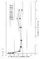
- FIG. 3 illustrates the relationship between a reverse leakage current and the thickness of the cap layer 6b with respect to the same HEMT devices.
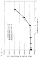
- FIG. 4 illustrates the relationship between a contact resistance and the thickness of the cap layer 6b with respect to the same HEMT devices.
- the value is highest when the thickness of the cap layer 6b is 0 nm (in other words, when the cap layer 6b is not provided), and the value sharply drops until the thickness of the cap layer 6b reaches 0.5 nm, and when the thickness of the cap layer 6b is 0.5 nm or more, the value remains almost unchanged at a value (0.5 nm or less) smaller than the value obtained when the thickness of the cap layer 6b is 0 nm.
- the surface of the cap layer 6b is more flattened than the surface of the barrier layer 5.
- the contact resistance is almost constant at a value equal to or less than 1.0 ⁇ 10 -5 / ⁇ cm 2 , while when the thickness of the cap layer 6b exceeds 6 nm, the contact resistance rapidly increases. This result indicates that it is preferable that the cap layer 6b has a thickness of 6 nm or less from the viewpoint of keeping a contact resistance of an ohmic electrode at a sufficiently low value.
- the cap layer 6b with a thickness of 0.5 nm or more and 6 nm or less.
- the HEMT device 20 includes the intermediate layer 6a provided between the barrier layer 5 and the cap layer 6b. This is for the purpose of keeping a high mobility of the two-dimensional electron gas. More specifically, providing the above-described cap layer 6b directly on the barrier layer 5 reduces the mobility of the two-dimensional electron gas, and therefore, in this embodiment, to suppress such reduction, the intermediate layer 6a is formed on the barrier layer 5 and then the cap layer 6b is formed thereon.
- the thickness of the intermediate layer 6a is preferably 0.5 nm or more and 6 nm or less. Forming the intermediate layer 6a with a thickness of 0.5 nm or more achieves a higher mobility as compared with when the intermediate layer 6a is not provided.
- the upper limit of the thickness of the intermediate layer 6a may be set within a range where a sheet resistance is kept so low that no influence is given on it. For example, in a case where the thickness of the cap layer 6b is 0.5 nm or more and 6 nm or less, forming the intermediate layer 6a with a thickness of (0.5 nm or more and) 6 nm or less can reduce the sheet resistance to 300 ⁇ / ⁇ or less.
- the HEMT device 20 is also characterized in that the intermediate layer 6a and the cap layer 6b are formed over the whole surface of the barrier layer 5 so that they are uniformly provided not only immediately below the gate electrode 9 but also immediately below the source electrode 7 and the drain electrode 8.
- the function and effect of reduction in the reverse leakage current are obtained as long as the intermediate layer 6a and the cap layer 6b exist only immediately below the gate electrode 9, but to achieve such a configuration, a photolithography process, an etching process, and the like, are required, which may cause a cost increase.
- This embodiment forms the intermediate layer 6a and the cap layer 6b over the whole surface of the barrier layer 5, without those processes. Therefore, it can be also said that an HEMT device having excellent characteristics is achieved with suppression of the costs.
- a so-called recessed ohmic in which the cap layer 6b, the intermediate layer 6a, and the barrier layer 5 are partially removed by etching is performed prior to forming those electrodes, and then the source electrode 7 and the drain electrode 8 are formed on the barrier layer 5 exposed as a result of the etching.
- the preparation of the epitaxial substrate 10 can be performed by using a known MOCVD apparatus. More specifically, an MOCVD apparatus is used that is configured to feed, into a reactor, a metal organic (MO) source gas (TMI, TMA and TMG) for In, Al and Ga, an ammonia gas (NH 3 gas), a hydrogen gas, and a nitrogen gas.
- a metal organic (MO) source gas TMI, TMA and TMG
- NH 3 gas ammonia gas
- hydrogen gas a hydrogen gas
- nitrogen gas a nitrogen gas
- a (0001)-oriented 6H-SiC substrate having a diameter of two inches is prepared as the base substrate 1, and this base substrate 1 is placed on a susceptor provided in a reactor of the MOCVD apparatus.
- the inside of the reactor is vacuumed, and then, an atmosphere in a hydrogen/nitrogen mixed flow state is created while a pressure inside the reactor is kept at a predetermined value in the range from 5 kPa to 50 kPa. In this condition, the susceptor is heated to thereby raise the temperature of the substrate.
- the temperature of the susceptor reaches a predetermined temperature in the range from 950°C to 1250°C (for example, 1050°C), which is a buffer layer formation temperature, an Al source gas and a NH 3 gas are introduced into the reactor, and thereby an AlN layer serving as the buffer layer 2 is formed.
- the channel layer formation temperature T1 is a value determined in a temperature range of 950°C or more and 1250°C or less in accordance with a value of an AlN mole fraction y1 in the channel layer 3.
- a pressure can be appropriately selected from the range from 10 kPa to an atmospheric pressure (100 kPa).
- a nitrogen gas atmosphere inside the reactor is maintained while the temperature of the susceptor is kept.
- the pressure in the reactor is set to be 10 kPa, and then a metal organic source gas and an ammonia gas are introduced into the reactor, so that an In x3 Al y3 Ga z3 N layer serving as the spacer layer 4 is formed with a predetermined thickness.
- the temperature of the susceptor is kept at a predetermined barrier layer formation temperature that is 650°C or more and 800°C or less, and the pressure in the reactor is kept at a predetermined value in the range from 1 kPa to 30 kPa.
- an ammonia gas and a metal organic source gas with a flow ratio in accordance with the composition of the barrier layer 5 are introduced into the reactor such that the so-called V/III ratio has a predetermined value of 3000 or more and 20000 or less.
- the temperature of the susceptor is set to be a predetermined intermediate layer formation temperature.
- a TMG and a NH 3 gas are fed, so that a GaN layer serving as the intermediate layer 6a is formed with a predetermined thickness.
- the temperature of the susceptor is set to be a predetermined cap layer formation temperature.
- a TMA and a NH 3 gas are fed, so that an AlN layer serving as the cap layer 6b is formed with a predetermined thickness.
- the preparation of the epitaxial substrate 10 is completed.
- the epitaxial substrate 10 After the formation of the epitaxial substrate 10, this is used to prepare an HEMT device. Subsequent steps are achieved through a known method.
- multilayer metal patterns serving as the source electrode 7 and the drain electrode 8 are formed in expected formation positions on the cap layer 6b.
- the epitaxial substrate 10 having these source electrode 7 and drain electrode 8 formed thereon is subjected to a heat treatment for several tens of seconds in a nitrogen gas atmosphere at a predetermined temperature of 650°C to 1000°C.
- a multilayer metal pattern serving as the gate electrode 9 is formed in an expected formation position on the cap layer 6b.
- a resultant is singulated into chips each having a predetermined size. Thereby, a large number of HEMT devices 20 are obtained. On the HEMT device 20 thus obtained, die bonding and wire bonding are performed as appropriate.
- an intermediate layer made of GaN is provided on a barrier layer, and a cap layer made of AlN is additionally provided, and a gate electrode is formed on the cap layer with a Schottky junction, to form an MIS junction.
- an HEMT device the aspect of forming an MIS junction between a gate electrode and a barrier layer is also applicable to other electronic devices using a Schottky junction, such as a Schottky barrier diode and a photosensor.
- the cap layer 6b is made of AlN.
- the cap layer 6b may be made of a group-III nitride having insulating properties and having a band gap larger than that of the second group-III nitride.
- a group-III nitride having insulating properties means a group-III nitride whose specific resistance is 10 8 ⁇ cm or more.
- the epitaxial substrate 10 according to the above-described embodiment including the intermediate layer 6a and the cap layer 6b was prepared, and evaluated for the two-dimensional electron gas concentration, the mobility of the two-dimensional electron gas, and the sheet resistance. Then, by using this epitaxial substrate 10, four types of HEMT devices 20 were prepared which were different from one another in terms of the configuration of the gate electrode 9. Each of the HEMT devices 20 was evaluated for a reverse leakage current caused upon application of -100V.
- a comparative example 1 an epitaxial substrate including neither the intermediate layer 6a nor the cap layer 6b was prepared, and evaluated for the two-dimensional electron gas concentration, the mobility of the two-dimensional electron gas, and the sheet resistance. Then, similarly to the example 1, the gate electrode 9 was formed on this epitaxial substrate, to thereby prepare four types of HEMT devices. Each of the HEMT devices was evaluated for a reverse leakage current caused upon application of -100V.
- an epitaxial substrate not including the intermediate layer 6a and including only the cap layer 6b was prepared, and evaluated for the two-dimensional electron gas concentration, the mobility of the two-dimensional electron gas, and the sheet resistance.
- the gate electrode 9 was formed on the epitaxial substrate, to thereby prepare four types of HEMT devices. Each of the HEMT devices was evaluated for a reverse leakage current caused upon application of -100V.
- the epitaxial substrate 10 was prepared. Until the formation of the spacer layer 4, all the epitaxial substrates 10 were prepared under the same conditions.
- a plurality of (0001)-oriented 6H-SiC substrates having a diameter of two inches were prepared as the base substrate 1.
- the thickness thereof was 300 ⁇ m.
- Each of the substrates was placed in a reactor of an MOCVD apparatus, and the inside of the reactor was vacuumed. Then, the pressure in the reactor was set to be 30 kPa, and an atmosphere in a hydrogen/nitrogen mixed flow state was created. Then, the susceptor was heated, to thereby raise the temperature of the base substrate 1.
- a TMA bubbling gas and an ammonia gas were introduced into the reactor, and an AlN layer having a thickness of 200 nm was formed as the buffer layer.
- the temperature of the susceptor was set to be a predetermined temperature
- a TMG bubbling gas serving as the metal organic source gas and an ammonia gas were introduced into the reactor with a predetermined flow ratio.
- a GaN layer serving as the channel layer 3 was formed with a thickness of 2 ⁇ m.
- the pressure in the reactor was set to be 10 kPa, and then a TMA bubbling gas and an ammonia gas were introduced into the reactor.
- a TMA bubbling gas and an ammonia gas were introduced into the reactor.
- an AlN layer having a thickness of 1 nm was formed as the spacer layer 4.
- the barrier layer 5 was then formed with a thickness of 15 nm.
- the composition of the barrier layer 5 was In 0.18 Al 0.82 N.
- the temperature of the susceptor was 745°C.
- the temperature of the susceptor was kept at 745°C which is the barrier layer formation temperature, and in this condition a GaN layer serving as the intermediate layer 6a was formed with a thickness of 3 nm, and then an AlN layer serving as the cap layer 6b was formed with a thickness of 3 nm.
- the cap layer 6b was formed with a thickness of 3 nm. In the comparative example 1, nothing was formed.
- each of the epitaxial substrates after the final layer was formed, the temperature of the susceptor was lowered to the vicinity of a room temperature, and the inside of the reactor was returned to the atmospheric pressure. Then, the prepared epitaxial substrates 10 were taken out. Through the above-described procedures, each of the epitaxial substrates 10 was obtained.
- an electrode pattern made of Ti/Al/Ni/Au (with film thicknesses of 25/75/15/100 nm, respectively) was formed on an upper surface of each epitaxial substrate in expected formation positions where the source electrode 7 and the drain electrode 8 were to be formed. Then, a heat treatment was performed in nitrogen for 30 seconds at 800°C.
- a pattern of the gate electrode 9 was formed on the upper surface of each epitaxial substrate in an expected formation position where the gate electrode 9 was to be formed.
- four types of gate electrodes 9 in total were formed, namely, a single layer metal electrode (12 nm) made of Au only and three types of multilayer metal electrodes made of Ni/Au (with film thicknesses of 6 nm / 12 nm), Pd/Au (with film thicknesses of 6 nm / 12 nm), and Pt/Au (with film thicknesses of 6 nm / 12 nm).
- the gate electrode 9 was formed such that the gate length was 1 ⁇ m, the gate width was 100 ⁇ m, the interval between the gate electrode 9 and the source electrode 7 was 2 ⁇ m, and the interval between the gate electrode 9 and the drain electrode was 10 ⁇ m.
- Table 1 shows a list of, with respect to each of the HEMT devices, the configurations of the intermediate layer 6a and the cap layer 6b of the epitaxial substrate, the two-dimensional electron gas concentration, the mobility of the two-dimensional electron gas, the sheet resistance, the configuration of the gate electrode of the HEMT device, and a result of measurement of the reverse leakage current caused upon application of -100V.
- the reverse leakage current was suppressed to the same level as in the example 1, but the mobility of the two-dimensional electron gas was lower than in the example 1 and the comparative example 1 while the sheet resistance was higher than in the example 1 and the comparative example 1.
- cap layer 6b with the intermediate layer 6a being provided on the barrier layer 5 exerts an effect in terms of reducing the reverse leakage current while maintaining a good two-dimensional electron gas concentration and a good sheet resistance.
- HEMT devices whose intermediate layers 6a had different thicknesses, including a case of providing no intermediate layer 6a, were prepared. More specifically, the HEMT devices were prepared through the same procedures as in the example 1, except that the thickness of the intermediate layer 6a was varied in eight levels of 0 nm, 0.1 nm, 0.5 nm, 1.5 nm, 3 nm, 6 nm, 8nm, and 10 nm and that the material of the gate electrode 9 was only Ni/Au (with film thicknesses of 6 nm/12nm).
- Table 2 shows a list of, with respect to each of the HEMT devices, the film thickness of the epitaxial substrate, the two-dimensional electron gas concentration, the mobility of the two-dimensional electron gas, the sheet resistance, and a result of measurement of the reverse leakage current caused in the HEMT device upon application of -100V.
- the thickness of the intermediate layer 6a when the thickness of the intermediate layer 6a is 0.5 nm or more, the value of the mobility of the two-dimensional electron gas is higher than when the intermediate layer 6a is not provided.
- the thickness of the intermediate layer 6a is 6 nm or less, the value of the two-dimensional electron gas concentration is at a similar level to that obtained when the intermediate layer 6a is not provided.
- the sheet resistance is kept at a value equal to or less than 300 ⁇ / ⁇ , which is lower than when the intermediate layer 6a is not provided.
- the intermediate layer 6a with a thickness of 0.5 nm or more between the cap layer 6b and the barrier layer 5 achieves an HEMT device in which a leakage current is reduced and the mobility of a two-dimensional electron gas is high. It is further revealed that forming the intermediate layer 6a with a thickness of 6 nm or less achieves an HEMT device having a high two-dimensional electron gas concentration and a low sheet resistance.
Landscapes
- Junction Field-Effect Transistors (AREA)
- Chemical & Material Sciences (AREA)
- Engineering & Computer Science (AREA)
- Materials Engineering (AREA)
Abstract
Description
- The present invention relates to a semiconductor device, and particularly to a semiconductor device in which a Schottky diode junction is established between an epitaxial substrate having a multilayer structure made of a group-III nitride semiconductor and a metal electrode.
- A group-III nitride semiconductor is attracting attention as a semiconductor material for a next-generation high-frequency/high-power device, because the nitride semiconductor has a high breakdown electric field and a high saturation electron velocity. For example, an HEMT (high electron mobility transistor) device in which a barrier layer made of AlGaN and a channel layer made of GaN are laminated takes advantage of the feature that causes a high-concentration two-dimensional electron gas (2DEG) to occur in a lamination interface (hetero interface) due to the large polarization effect (a spontaneous polarization effect and a piezo polarization effect) specific to a nitride material (for example, see Non-Patent Document 1).
- In some cases, a single crystal (a different kind single crystal) having a composition different from that of a group-III nitride, such as silicon and SiC, is used as a base substrate of an HEMT-device substrate. In this case, a buffer layer such as a strained-superlattice layer or a low-temperature growth buffer layer is generally formed as an initially-grown layer on the base substrate. Accordingly, a configuration in which a barrier layer, a channel layer, and a buffer layer are epitaxially formed on a base substrate is the most basic configuration of the HEMT-device substrate including a base substrate made of a different kind single crystal. Additionally, a spacer layer having a thickness of about 1 nm may be sometimes provided between the barrier layer and the channel layer, for the purpose of facilitating a spatial confinement of the two-dimensional electron gas. The spacer layer is made of, for example, AlN. Moreover, a cap layer made of, for example, an n-type GaN layer or a superlattice layer may be sometimes formed on the barrier layer, for the purpose of controlling the energy level at the most superficial surface of the HEMT-device substrate and improving contact characteristics of contact with an electrode.
- For example, it is known that, in a case where a nitride HEMT device has the most general configuration in which a channel layer is made of GaN and a barrier layer is made of AlGaN, the concentration of a two-dimensional electron gas existing in an HEMT-device substrate increases as the AlN mole fraction in AlGaN of the barrier layer increases (for example, see Non-Patent Document 2). If the concentration of the two-dimensional electron gas can be considerably increased, the controllable current density of the HEMT device, that is, the power density that can be handled, would be considerably improved.
- Also attracting attention is an HEMT device having a structure with reduced strain, such as an HEMT device in which a channel layer is made of GaN and a barrier layer is made of InAlN, in which the dependence on a piezo polarization effect is small and almost only a spontaneous polarization is used to generate a two-dimensional electron gas with a high concentration (for example, see Non-Patent Document 3).
- In a case of preparing an HEMT device including a channel layer made of GaN and a barrier layer made of InAlN, a junction formed between a gate electrode and the barrier layer is generally a Schottky junction. In this case, however, depending on the composition of the InAlN layer and the conditions under which the InAlN layer has been formed, there is a possibility that a large leakage current occurs when a reverse voltage is applied to the Schottky junction.
- Forming a contact layer made of AlN on the InAlN layer can reduce the leakage current. However, an HEMT device having such a configuration involves a problem that the mobility of a two-dimensional electron gas is low. The cause thereof is assumed to be occurrence of strain in the InAlN layer due to the lattice constant of the AlN layer being smaller than that of the InAlN layer.
- Non-Patent Document 1: "Highly Reliable 250W High Electron Mobility Transistor Power Amplifier", TOSHIHIDE KIKKAWA, Jpn. J. Appl. Phys. 44, (2005), 4896
- Non-Patent Document 2: "Gallium Nitride Based High Power Heterojunction Field Effect Transistors: process Development and Present Status at USCB", Stacia Keller, Yi-Feng Wu, Giacinta Parish, Naiqian Ziang, Jane J. Xu, Bernd P. Keller, Steven P. DenBaars, and Umesh K. Mishra, IEEE Trans. Electron Devices 48, (2001), 552
- Non-Patent Document 3: "Can InAlN/GaN be an alternative to high power/high temperature AlGaN/GaN devices?", F. Medjdoub, J.-F. Carlin, M. Gonschorek, E. Feltin, M.A. Py, D. Ducatteau, C. Gaquiere, N. Grandjean, and E. Kohn, IEEE IEDM Tech. Digest in IEEE IEDM 2006, 673
- The present invention has been made in view of the problems described above, and an object of the present invention is to provide a semiconductor device in which a reverse leakage current is suppressed and the mobility of a two-dimensional electron gas is high.
- To solve the problems described above, a first aspect of the present invention is a semiconductor device including: an epitaxial substrate in which a group of group-III nitride layers are laminated on a base substrate such that a (0001) crystal plane is substantially in parallel with a substrate surface; and a Schottky electrode. The epitaxial substrate includes: a channel layer made of a first group-III nitride having a composition of Inx1Aly1Gaz1N (x1+y1+z1=1, z1>0); a barrier layer made of a second group-III nitride having a composition of Inx2Aly2N (x2+y2=1, x2>0, y2>0); an intermediate layer made of GaN and adjacent to the barrier layer; and a cap layer made of AlN and adjacent to the intermediate layer. The Schottky electrode is bonded to the cap layer.
- A second aspect of the present invention is the semiconductor device according to the first aspect, wherein the intermediate layer has a film thickness of 0.5 nm or more.
- A third aspect of the present invention is the semiconductor device according to the second aspect, wherein the intermediate layer has a film thickness of 6 nm or less.
- A fourth aspect of the present invention is the semiconductor device according to any one of the first to third aspects, wherein the cap layer has a film thickness of 0.5 nm or more and 6 nm or less.
- A fifth aspect of the present invention is the semiconductor device according to any one of the first to fourth aspects, wherein the band gap of the second group-III nitride is larger than the band gap of the first group-III nitride.
- A sixth aspect of the present invention is the semiconductor device according to any one of the first to fifth aspects, wherein the Schottky electrode contains at least one of Ni, Pt, Pd, and Au.
- A seventh aspect of the present invention is the semiconductor device according to any one of the first to sixth aspects, wherein the cap layer has a root-mean-square surface roughness of 0.5 nm or less.
- An eighth aspect of the present invention is the semiconductor device according to any one of the first to seventh aspects, wherein the second group-III nitride is Inx2Aly2N (x2+y2=1, 0.14≤x2≤0.24).
- A ninth aspect of the present invention is the semiconductor device according to any one of the first to eighth aspects, wherein the first group-III nitride is Aly1Gaz1N (y1+z1=1, z1>0).
- A tenth aspect of the present invention is the semiconductor device according to the ninth aspect, wherein the first group-III nitride is GaN.
- An eleventh aspect of the present invention is the semiconductor device according to the ninth or tenth aspect, further including a spacer layer provided between the channel layer and the barrier layer, the spacer layer being made of a third group-III nitride having a composition of Inx3Aly3Gaz3N (x3+y3+z3=1, y3>0) and having a band gap larger than that of the second group-III nitride.
- A twelfth aspect of the present invention is the semiconductor device according to the eleventh aspect, wherein the third group-III nitride is AlN.
- A thirteenth aspect of the present invention is the semiconductor device according to any one of the first to twelfth aspects, wherein an ohmic electrode as well as the Schottky electrode is bonded to the cap layer.
- A fourteenth aspect of the present invention is an HEMT device that is the semiconductor device according to the thirteenth aspect, including the Schottky electrode serving as a gate electrode, and the ohmic electrodes serving as a source electrode and a drain electrode.
- A fifteenth aspect of the present invention is a method of manufacturing a semiconductor device. The semiconductor device includes: an epitaxial substrate in which a group of group-III nitride layers are laminated on a base substrate such that a (0001) crystal plane is substantially in parallel with a substrate surface; and a Schottky electrode. The method includes: a channel layer formation step of forming a channel layer on a base substrate, the channel layer being made of a first group-III nitride having a composition of Inx1Aly1Gaz1N (x1+y1+z1=1, z1>0); a barrier layer formation step of forming a barrier layer on the channel layer, the barrier layer being made of a second group-III nitride having a composition of Inx2Aly2N (x2+y2=1, x2>0, y2>0); an intermediate layer formation step of forming an intermediate layer, the intermediate layer being made of GaN and adjacent to the barrier layer; a cap layer formation step of forming a cap layer, the cap layer being made of AlN and adjacent to the intermediate layer; and a Schottky electrode formation step of forming a Schottky electrode, the Schottky electrode being bonded to the cap layer.
- A sixteenth aspect of the present invention is the method of manufacturing the semiconductor device according to the fifteenth aspect, wherein the intermediate layer is formed with a thickness of 0.5 nm or more.
- A seventeenth aspect of the present invention is the method of manufacturing the semiconductor device according to the sixteenth aspect, wherein the intermediate layer is formed with a thickness of 6 nm or less.
- An eighteenth aspect of the present invention is the method of manufacturing the semiconductor device according to any one of the fifteenth to seventeenth aspects, wherein the cap layer is formed with a thickness of 0.5 nm or more and 6 nm or less.
- A nineteenth aspect of the present invention is the method of manufacturing the semiconductor device according to any one of the fifteenth to eighteenth aspects, wherein the band gap of the second group-III nitride is larger than the band gap of the first group-III nitride.
- A twentieth aspect of the present invention is the method of manufacturing the semiconductor device according to any one of the fifteenth to nineteenth aspects, wherein, in the Schottky electrode formation step, the Schottky electrode is formed so as to contain at least one ofNi, Pt, Pd, and Au.
- A twenty-first aspect of the present invention is the method of manufacturing the semiconductor device according to any one of the fifteenth to twentieth aspects, wherein the second group-III nitride is Inx2Aly2N (x2+y2=1, 0.14≤x2≤0.24).
- A twenty-second aspect of the present invention is the method of manufacturing the semiconductor device according to any one of the fifteenth to twenty-first aspects, wherein the first group-III nitride is Aly1Gaz1N (y1+z1=1, z1>0).
- A twenty-third aspect of the present invention is the method of manufacturing the semiconductor device according to the twenty-second aspect, wherein the first group-III nitride is GaN.
- A twenty-fourth aspect of the present invention is the method of manufacturing the semiconductor device according to the twenty-second or twenty-third aspect, further including a spacer layer formation step of forming a spacer layer between the channel layer and the barrier layer, the spacer layer being made of a third group-III nitride having a composition of Inx3Aly3Gaz3N (x3+y3+z3=1, y3>0) and having a band gap larger than that of the second group-III nitride.
- A twenty-fifth aspect of the present invention is the method of manufacturing the semiconductor device according to the twenty-fourth aspect, wherein the third group-III nitride is AlN.
- A twenty-sixth aspect of the present invention is the method of manufacturing the semiconductor device according to any one of the fifteenth to twenty-fifth aspects, further including an ohmic electrode formation step of forming an ohmic electrode such that the ohmic electrode is bonded to the cap layer on which the Schottky electrode is formed.
- In the first to twenty-sixth aspects of the present invention, the intermediate layer made of GaN and the cap layer made of AlN are provided on the barrier layer in the mentioned order, and an electrode is formed on the cap layer with a Schottky junction, to form an MIS junction. This achieves a semiconductor device in which a reverse leakage current is suppressed and the mobility of a two-dimensional electron gas is kept high as compared with a case where an electrode is formed directly on a barrier layer with a Schottky junction.
-
- [
FIG. 1 ] A schematic cross-sectional view showing an outline configuration of anHEMT device 20 that is one aspect of a semiconductor device according to an embodiment of the present invention. - [
FIG. 2 ] A diagram illustrating the relationship between the surface roughness and thickness of acap layer 6b. - [
FIG. 3 ] A diagram illustrating the relationship between a reverse leakage current and thecap layer 6b. - [
FIG. 4 ] A diagram plotting a contact resistance of an ohmic electrode against the thickness of thecap layer 6b. -
FIG. 1 is a schematic cross-sectional view showing an outline configuration of anHEMT device 20 that is one aspect of a semiconductor device according to an embodiment of the present invention. Roughly, theHEMT device 20 has a configuration in which asource electrode 7, adrain electrode 8, and agate electrode 9 are arranged on anepitaxial substrate 10. More specifically, theepitaxial substrate 10 has a configuration in which abase substrate 1, abuffer layer 2, achannel layer 3, aspacer layer 4, a barrier layer 5, an intermediate layer 6a, and acap layer 6b are laminated. Additionally, thesource electrode 7, thedrain electrode 8, and thegate electrode 9 are formed on thecap layer 6b. The thickness ratio among the layers shown inFIG. 1 does not reflect the actual ratio. In one preferred example, all of thebuffer layer 2, thechannel layer 3, thespacer layer 4, the barrier layer 5, the intermediate layer 6a, and thecap layer 6b are epitaxially formed through a MOCVD process (Metal Organic Chemical Vapor Deposition) (details will be described later). - The following description is directed to a case where the MOCVD process is used for the formation of each layer. However, a method appropriately selected from other epitaxial growth processes including vapor deposition processes and liquid phase deposition processes such as MBE, HVPE, and LPE may be adopted, or different growth processes may be adopted in combination, as long as the method can form each of the layers with good crystallinity.
- No particular limitation is put on the
base substrate 1, as long as thebase substrate 1 allows a nitride semiconductor layer with good crystallinity to be formed thereon. In one preferable example, a single crystal 6H-SiC substrate is used. However, a substrate made of sapphire, Si, GaAs, spinel, MgO, ZnO, ferrite, or the like, may be adopted. - The
buffer layer 2 is a layer made of AlN, and formed with a thickness of about several hundreds nm, for the purpose of obtaining good crystal quality of thechannel layer 3, thespacer layer 4, the barrier layer 5, the intermediate layer 6a, and thecap layer 6b which will be formed on thebuffer layer 2. In one preferable example, thebuffer layer 2 is formed with a thickness of 200 nm. - The
channel layer 3 is a layer made of a group-III nitride (first group-III nitride) having a composition of Inx1Aly1Gaz1N (x1+y1+z1=1), and formed with a thickness of about several µm. Thechannel layer 3 is preferably made of a group-III nitride having a composition of Aly1Gaz1N (y1+z1=1, z1>0), and more preferably made of GaN. - The barrier layer 5 is a layer made of a group-III nitride (second group-III nitride) having a composition of Inx2Aly2N (x2+y2=1, x2>, y2>0), and formed with a thickness of about several nm to several tens of nm. Preferably, 0.14≤x2≤0.24 is satisfied. The value of x2 being outside this range is not preferable, because strain acting on the barrier layer 5 exceeds ±0.5%, at which crystal strain starts to increase its influence on the reliability of a Schottky junction.
- The
channel layer 3 and the barrier layer 5 are formed so as to satisfy such composition ranges that a band gap of the second group-III nitride constituting the latter is greater than a band gap of the first group-III nitride constituting the former. - The intermediate layer 6a is a layer made of GaN. The
cap layer 6b is a layer made of AlN. Functions and effects exerted by providing of these intermediate layer 6a and thecap layer 6b in theHEMT device 20 will be described later. - Moreover, the
spacer layer 4 is provided between thechannel layer 3 and the barrier layer 5. Thespacer layer 4 is a layer made of a group-III nitride (third group-III nitride) having a composition of Inx3Aly3Gaz3N (x3+y3+z3=1) and containing at least Al (that satisfies y3>0), and formed with a thickness in the range from 0.5 nm to 1.5 nm. - In the
epitaxial substrate 10 having such a layer configuration, a two-dimensionalelectron gas region 3e, in which a two-dimensional electron gas exists with a high concentration, is formed at an interface between thechannel layer 3 and the spacer layer 4 (more specifically, in a portion of thechannel layer 3 near this interface). - Preferably, the
spacer layer 4 and the barrier layer 5 are formed so as to satisfy such composition ranges that a band gap of the third group-III nitride constituting the former is equal to or greater than the band gap of the second group-III nitride constituting the latter. In such a case, an alloy scattering effect is suppressed, and the concentration and the mobility of a two-dimensional electron gas are improved. More preferably, thespacer layer 4 is made of AlN (x3=0, y3=1, z3=0). In this case, thespacer layer 4 is a binary compound of Al and N, which can increase the suppression of the alloy scattering effect as compared with a ternary compound containing Ga. This improves the concentration and mobility of the two-dimensional electron gas. The discussion about these composition ranges does not exclude that thespacer layer 4 contains impurities. - However, it is not essential that the
spacer layer 4 is provided in theepitaxial substrate 10. It may be also acceptable that the barrier layer 5 is formed directly on thechannel layer 3. In this case, the two-dimensionalelectron gas region 3e is formed at an interface between thechannel layer 3 and the barrier layer 5. - Each of the
source electrode 7 and thedrain electrode 8 is a multilayer metal electrode in which each metal layer has a thickness of about more than ten nm to one hundred and several tens of nm. Each of thesource electrode 7 and thedrain electrode 8 has an ohmic contact with thecap layer 6b. A metal used for thesource electrode 7 and thedrain electrode 8 may be made of a metal material that provides a good ohmic contact relative to the epitaxial substrate 10 (relative to thecap layer 6b). It is preferable that multilayer metal electrodes made of Ti/Al/Ni/Au are formed as thesource electrode 7 and thedrain electrode 8. However, this is not limiting. For example, a multilayer metal electrode made of Ti/Al/Pt/Au or Ti/Al may be formed. The formation of thesource electrode 7 and thedrain electrode 8 can be implemented through a photolithography process and a vacuum vapor deposition process. - On the other hand, the
gate electrode 9 is a single-layer or multilayer metal electrode in which one or more metal layers are formed with a thickness of about more than ten nm to one hundred and several tens of nm. Thegate electrode 9 has a Schottky contact with the barrier layer 5. It is preferable that thegate electrode 9 is formed by using, as a material thereof, a metal having a high work function, such as Pd, Pt, Ni, or Au. Alternatively, it may be possible that a multilayer metal film consisted of some of the above-mentioned metals or consisted of some of the above-mentioned metals and Al, for example, is formed as thegate electrode 9. Since thecap layer 6b made of AlN is provided, not only the above-mentioned materials but also a metal material that is used for forming an ohmic junction with a group-III nitride semiconductor is also adoptable as a material of thegate electrode 9. For example, a multilayer metal film containing Ti/Al may be formed. This is because, in such a case, a junction is made between AlN having a wide band gap and a metal material having a relatively low work function, which allows a Schottky contact to be relatively easily obtained. The formation of thegate electrode 9 can be implemented through a photolithography process and a vacuum vapor deposition process. - In the
HEMT device 20 having the above-described configuration, thegate electrode 9, thecap layer 6b, and the barrier layer 5 (more exactly, with interposition of the intermediate layer 6a) form a so-called MIS (metal-insulator-semiconductor) junction. Since theHEMT device 20 has such an MIS junction, in principle, a reverse leakage current is suppressed as compared with a conventional HEMT device in which thegate electrode 9 has a Schottky junction directly with the barrier layer 5. A specific value varies depending on, for example, the composition and the thickness of each part. In a case where theHEMT device 20 has the configuration described in this embodiment, for example, a leakage current caused upon application of -100V is suppressed down to about 1/100 to 1/1000 of a leakage current occurring in a case where a gate electrode is formed directly on a barrier layer. -
FIGS. 2 to 4 are diagrams for explaining an effect exerted by the HEMT device in which thecap layer 6b is provided immediately below thegate electrode 9, that is, an effect exerted by the HEMT device having the above-described MIS junction. More specifically,FIG. 2 illustrates the relationship between the surface roughness and the thickness of thecap layer 6b with respect to three types of HEMT devices whose barrier layers 5 have three different levels of compositions, namely, In0.14Al0.86N, In0.18Al0.82N, and In0.24Al0.76N. However, for convenience of discussion, the intermediate layer 6a is not provided in these HEMT devices.FIG. 3 illustrates the relationship between a reverse leakage current and the thickness of thecap layer 6b with respect to the same HEMT devices.FIG. 4 illustrates the relationship between a contact resistance and the thickness of thecap layer 6b with respect to the same HEMT devices. - In
FIGS. 2 and3 , the value is highest when the thickness of thecap layer 6b is 0 nm (in other words, when thecap layer 6b is not provided), and the value sharply drops until the thickness of thecap layer 6b reaches 0.5 nm, and when the thickness of thecap layer 6b is 0.5 nm or more, the value remains almost unchanged at a value (0.5 nm or less) smaller than the value obtained when the thickness of thecap layer 6b is 0 nm. This means that forming thecap layer 6b with a thickness of 0.5 nm or more can improve the surface flatness thereof and providing thegate electrode 9 on thecap layer 6b having such an excellent surface flatness can reduce the reverse leakage current. The surface of thecap layer 6b is more flattened than the surface of the barrier layer 5. - In
FIG. 4 , when the thickness of thecap layer 6b is 6 nm or less, the contact resistance is almost constant at a value equal to or less than 1.0×10⁻⁵/Ωcm2, while when the thickness of thecap layer 6b exceeds 6 nm, the contact resistance rapidly increases. This result indicates that it is preferable that thecap layer 6b has a thickness of 6 nm or less from the viewpoint of keeping a contact resistance of an ohmic electrode at a sufficiently low value. - From the above, it is preferable to form the
cap layer 6b with a thickness of 0.5 nm or more and 6 nm or less. - The
HEMT device 20 according to this embodiment includes the intermediate layer 6a provided between the barrier layer 5 and thecap layer 6b. This is for the purpose of keeping a high mobility of the two-dimensional electron gas. More specifically, providing the above-describedcap layer 6b directly on the barrier layer 5 reduces the mobility of the two-dimensional electron gas, and therefore, in this embodiment, to suppress such reduction, the intermediate layer 6a is formed on the barrier layer 5 and then thecap layer 6b is formed thereon. - The thickness of the intermediate layer 6a is preferably 0.5 nm or more and 6 nm or less. Forming the intermediate layer 6a with a thickness of 0.5 nm or more achieves a higher mobility as compared with when the intermediate layer 6a is not provided. The upper limit of the thickness of the intermediate layer 6a may be set within a range where a sheet resistance is kept so low that no influence is given on it. For example, in a case where the thickness of the
cap layer 6b is 0.5 nm or more and 6 nm or less, forming the intermediate layer 6a with a thickness of (0.5 nm or more and) 6 nm or less can reduce the sheet resistance to 300Ω/□ or less. - The
HEMT device 20 according to this embodiment is also characterized in that the intermediate layer 6a and thecap layer 6b are formed over the whole surface of the barrier layer 5 so that they are uniformly provided not only immediately below thegate electrode 9 but also immediately below thesource electrode 7 and thedrain electrode 8. In fact, the function and effect of reduction in the reverse leakage current are obtained as long as the intermediate layer 6a and thecap layer 6b exist only immediately below thegate electrode 9, but to achieve such a configuration, a photolithography process, an etching process, and the like, are required, which may cause a cost increase. This embodiment forms the intermediate layer 6a and thecap layer 6b over the whole surface of the barrier layer 5, without those processes. Therefore, it can be also said that an HEMT device having excellent characteristics is achieved with suppression of the costs. Needless to say, it may be also possible that, in order to form thesource electrode 7 and thedrain electrode 8 directly on the barrier layer 5, a so-called recessed ohmic in which thecap layer 6b, the intermediate layer 6a, and the barrier layer 5 are partially removed by etching is performed prior to forming those electrodes, and then thesource electrode 7 and thedrain electrode 8 are formed on the barrier layer 5 exposed as a result of the etching. - Next, a method for preparing the
HEMT device 20 having the above-described configuration will be described. - The preparation of the
epitaxial substrate 10 can be performed by using a known MOCVD apparatus. More specifically, an MOCVD apparatus is used that is configured to feed, into a reactor, a metal organic (MO) source gas (TMI, TMA and TMG) for In, Al and Ga, an ammonia gas (NH3 gas), a hydrogen gas, and a nitrogen gas. - Firstly, for example, a (0001)-oriented 6H-SiC substrate having a diameter of two inches is prepared as the
base substrate 1, and thisbase substrate 1 is placed on a susceptor provided in a reactor of the MOCVD apparatus. The inside of the reactor is vacuumed, and then, an atmosphere in a hydrogen/nitrogen mixed flow state is created while a pressure inside the reactor is kept at a predetermined value in the range from 5 kPa to 50 kPa. In this condition, the susceptor is heated to thereby raise the temperature of the substrate. - When the temperature of the susceptor reaches a predetermined temperature in the range from 950°C to 1250°C (for example, 1050°C), which is a buffer layer formation temperature, an Al source gas and a NH3 gas are introduced into the reactor, and thereby an AlN layer serving as the
buffer layer 2 is formed. - After the formation of the AlN layer, the temperature of the susceptor is kept at a predetermined channel layer formation temperature, and a metal organic source gas and an ammonia gas are introduced into the reactor in accordance with the composition of the
channel layer 3, and thereby an Inx1Aly1Gaz1N layer (x1=0, 0≤y1≤0.3) serving as thechannel layer 3 is formed. Here, the channel layer formation temperature T1 is a value determined in a temperature range of 950°C or more and 1250°C or less in accordance with a value of an AlN mole fraction y1 in thechannel layer 3. No particular limitation is put on the pressure in the reactor at a time when thechannel layer 3 is formed. A pressure can be appropriately selected from the range from 10 kPa to an atmospheric pressure (100 kPa). - After the formation of the Inx1Aly1Gaz1N layer, a nitrogen gas atmosphere inside the reactor is maintained while the temperature of the susceptor is kept. The pressure in the reactor is set to be 10 kPa, and then a metal organic source gas and an ammonia gas are introduced into the reactor, so that an Inx3Aly3Gaz3N layer serving as the
spacer layer 4 is formed with a predetermined thickness. - After the formation of the Inx3Aly3Gaz3N layer, then, in order to form an Inx2Aly2N serving as the barrier layer 5, the temperature of the susceptor is kept at a predetermined barrier layer formation temperature that is 650°C or more and 800°C or less, and the pressure in the reactor is kept at a predetermined value in the range from 1 kPa to 30 kPa. Then, an ammonia gas and a metal organic source gas with a flow ratio in accordance with the composition of the barrier layer 5 are introduced into the reactor such that the so-called V/III ratio has a predetermined value of 3000 or more and 20000 or less.
- After the formation of the Inx3Aly3Gaz3N layer, then the temperature of the susceptor is set to be a predetermined intermediate layer formation temperature. In this condition, a TMG and a NH3 gas are fed, so that a GaN layer serving as the intermediate layer 6a is formed with a predetermined thickness.
- After the formation of the GaN layer, then the temperature of the susceptor is set to be a predetermined cap layer formation temperature. In this condition, a TMA and a NH3 gas are fed, so that an AlN layer serving as the
cap layer 6b is formed with a predetermined thickness. Upon the formation of thecap layer 6b, the preparation of theepitaxial substrate 10 is completed. - After the formation of the
epitaxial substrate 10, this is used to prepare an HEMT device. Subsequent steps are achieved through a known method. - Firstly, through a photolithography process and a vacuum vapor deposition process, multilayer metal patterns serving as the
source electrode 7 and thedrain electrode 8 are formed in expected formation positions on thecap layer 6b. - Then, in order to give excellent ohmic characteristics to the
source electrode 7 and thedrain electrode 8, theepitaxial substrate 10 having thesesource electrode 7 and drainelectrode 8 formed thereon is subjected to a heat treatment for several tens of seconds in a nitrogen gas atmosphere at a predetermined temperature of 650°C to 1000°C. - Then, through a photolithography process and a vacuum vapor deposition process, a multilayer metal pattern serving as the
gate electrode 9 is formed in an expected formation position on thecap layer 6b. - Then, a resultant is singulated into chips each having a predetermined size. Thereby, a large number of
HEMT devices 20 are obtained. On theHEMT device 20 thus obtained, die bonding and wire bonding are performed as appropriate. - As thus far described, in this embodiment, an intermediate layer made of GaN is provided on a barrier layer, and a cap layer made of AlN is additionally provided, and a gate electrode is formed on the cap layer with a Schottky junction, to form an MIS junction. This achieves an HEMT device in which a reverse leakage current is largely reduced and the mobility of the two-dimensional electron gas is high as compared with a case where a gate electrode is formed directly on a barrier layer with a Schottky junction.
- Although the description of the above-described embodiment has been given with respect to an HEMT device, the aspect of forming an MIS junction between a gate electrode and a barrier layer is also applicable to other electronic devices using a Schottky junction, such as a Schottky barrier diode and a photosensor.
- In the above-described embodiment, the
cap layer 6b is made of AlN. However, thecap layer 6b may be made of a group-III nitride having insulating properties and having a band gap larger than that of the second group-III nitride. Here, a group-III nitride having insulating properties means a group-III nitride whose specific resistance is 108 Ωcm or more. When the specific resistance is in this range, the above-described MIS junction is successfully formed. As long as the specific resistance satisfies this range, the presence of conductive impurities in thecap layer 6b is allowed. - In an example 1, the
epitaxial substrate 10 according to the above-described embodiment including the intermediate layer 6a and thecap layer 6b was prepared, and evaluated for the two-dimensional electron gas concentration, the mobility of the two-dimensional electron gas, and the sheet resistance. Then, by using thisepitaxial substrate 10, four types ofHEMT devices 20 were prepared which were different from one another in terms of the configuration of thegate electrode 9. Each of theHEMT devices 20 was evaluated for a reverse leakage current caused upon application of -100V. - In a comparative example 1, an epitaxial substrate including neither the intermediate layer 6a nor the
cap layer 6b was prepared, and evaluated for the two-dimensional electron gas concentration, the mobility of the two-dimensional electron gas, and the sheet resistance. Then, similarly to the example 1, thegate electrode 9 was formed on this epitaxial substrate, to thereby prepare four types of HEMT devices. Each of the HEMT devices was evaluated for a reverse leakage current caused upon application of -100V. - Furthermore, in a comparative example 2, an epitaxial substrate not including the intermediate layer 6a and including only the
cap layer 6b was prepared, and evaluated for the two-dimensional electron gas concentration, the mobility of the two-dimensional electron gas, and the sheet resistance. Then, similarly to the example 1, thegate electrode 9 was formed on the epitaxial substrate, to thereby prepare four types of HEMT devices. Each of the HEMT devices was evaluated for a reverse leakage current caused upon application of -100V. - That is, four types of
gate electrodes 9 having different configurations were formed on each of the three types of epitaxial substrates. Thus, twelve types of HEMT devices in total were obtained. - Firstly, the
epitaxial substrate 10 was prepared. Until the formation of thespacer layer 4, all theepitaxial substrates 10 were prepared under the same conditions. - To be specific, firstly, a plurality of (0001)-oriented 6H-SiC substrates having a diameter of two inches were prepared as the
base substrate 1. The thickness thereof was 300 µm. Each of the substrates was placed in a reactor of an MOCVD apparatus, and the inside of the reactor was vacuumed. Then, the pressure in the reactor was set to be 30 kPa, and an atmosphere in a hydrogen/nitrogen mixed flow state was created. Then, the susceptor was heated, to thereby raise the temperature of thebase substrate 1. - After the temperature of the susceptor reached 1050°C, a TMA bubbling gas and an ammonia gas were introduced into the reactor, and an AlN layer having a thickness of 200 nm was formed as the buffer layer.
- Then, the temperature of the susceptor was set to be a predetermined temperature, a TMG bubbling gas serving as the metal organic source gas and an ammonia gas were introduced into the reactor with a predetermined flow ratio. Thus, a GaN layer serving as the
channel layer 3 was formed with a thickness of 2 µm. - After the formation of the
channel layer 3, the pressure in the reactor was set to be 10 kPa, and then a TMA bubbling gas and an ammonia gas were introduced into the reactor. Thus, an AlN layer having a thickness of 1 nm was formed as thespacer layer 4. - After the formation of the
spacer layer 4, the barrier layer 5 was then formed with a thickness of 15 nm. The composition of the barrier layer 5 was In0.18Al0.82N. The temperature of the susceptor was 745°C. - After the formation of the barrier layer 5, in the example 1, the temperature of the susceptor was kept at 745°C which is the barrier layer formation temperature, and in this condition a GaN layer serving as the intermediate layer 6a was formed with a thickness of 3 nm, and then an AlN layer serving as the
cap layer 6b was formed with a thickness of 3 nm. In the comparative example 2, thecap layer 6b was formed with a thickness of 3 nm. In the comparative example 1, nothing was formed. - In each of the epitaxial substrates, after the final layer was formed, the temperature of the susceptor was lowered to the vicinity of a room temperature, and the inside of the reactor was returned to the atmospheric pressure. Then, the prepared
epitaxial substrates 10 were taken out. Through the above-described procedures, each of theepitaxial substrates 10 was obtained. - Then, a part of each of the epitaxial substrates was cut out in a singulating manner. A specimen to be evaluated thus obtained was subjected to Hall effect measurement. In this measurement, the two-dimensional electron gas concentration, the two-dimensional electron gas mobility, and the sheet resistance was obtained with respect to each of the epitaxial substrates.
- Then, through a photolithography process and a vacuum vapor deposition process, an electrode pattern made of Ti/Al/Ni/Au (with film thicknesses of 25/75/15/100 nm, respectively) was formed on an upper surface of each epitaxial substrate in expected formation positions where the
source electrode 7 and thedrain electrode 8 were to be formed. Then, a heat treatment was performed in nitrogen for 30 seconds at 800°C. - Then, through a photolithography process and a vacuum vapor deposition process, a pattern of the
gate electrode 9 was formed on the upper surface of each epitaxial substrate in an expected formation position where thegate electrode 9 was to be formed. Here, four types ofgate electrodes 9 in total were formed, namely, a single layer metal electrode (12 nm) made of Au only and three types of multilayer metal electrodes made of Ni/Au (with film thicknesses of 6 nm / 12 nm), Pd/Au (with film thicknesses of 6 nm / 12 nm), and Pt/Au (with film thicknesses of 6 nm / 12 nm). Thegate electrode 9 was formed such that the gate length was 1 µm, the gate width was 100 µm, the interval between thegate electrode 9 and thesource electrode 7 was 2 µm, and the interval between thegate electrode 9 and the drain electrode was 10 µm. - Finally, a resultant was singulated into chips. Thus, an HEMT device was obtained.
- Die bonding and wire bonding were performed on the obtained HEMT device, and then a reverse leakage current caused upon application of -100V was measured.
- Table 1 shows a list of, with respect to each of the HEMT devices, the configurations of the intermediate layer 6a and the
cap layer 6b of the epitaxial substrate, the two-dimensional electron gas concentration, the mobility of the two-dimensional electron gas, the sheet resistance, the configuration of the gate electrode of the HEMT device, and a result of measurement of the reverse leakage current caused upon application of -100V.[Table 1] Configuration of Epitaxial Substrate Two-Dimensional Electron Gas Concentration (/cm2) Mobility of Two-Dimensional Electron Gas (cm2/Vs) Sheet Resistance (Ω/□) Configuration of Gate Metal Leakage Current (A) (Upon Application of -100V) Example 1 Intermediate Layer: GaN ( Thickness 3 nm)2.35E+13 980 271 Ni/Au 1.46E-08 Pd/Au 1.04E-08 Cap Layer: AlN ( Thickness 3 nm)Pt/Au 4.62E-09 Au 1.12E-08 Comparative Example 1 Intermediate Layer: Non 2.30E+13 990 274 Ni/Au 2.88E-05 Pd/Au 1.92E-05 Cap Layer: Non Pt/Au 9.26E-06 Au 2.34E-05 Comparative Example 2 Intermediate Layer: Non 2.50E+13 650 384 Ni/Au 2.62E-08 Pd/Au 2.21E-08 Cap Layer: AlN ( Thickness 3 nm)Pt/Au 1.12E-08 Au 2.40E-08 - The results shown in Table 1 reveal that, in all the HEMT devices according to the example 1, that is, irrespective of the configuration of the
gate electrode 9, the reverse leakage currents were suppressed to about 1/100 to 1/1000 of the reverse leakage currents in the HEMT devices according to the comparative example 1 in which the preparation was performed under the same conditions except the intermediate layer 6a and thecap layer 6b. It is also revealed that there is almost no difference between the example 1 and the comparative example 1 in terms of the two-dimensional electron gas concentration, the mobility of the two-dimensional electron gas, and the sheet resistance. - On the other hand, in the HEMT devices according to the comparative example 2 in which the intermediate layer 6a was not provided and only the
cap layer 6b was provided, the reverse leakage current was suppressed to the same level as in the example 1, but the mobility of the two-dimensional electron gas was lower than in the example 1 and the comparative example 1 while the sheet resistance was higher than in the example 1 and the comparative example 1. - The above-described results indicate that providing the
cap layer 6b directly on the barrier layer 5 exerts an effect of reducing the leakage current, but on the other hand, has a disadvantage in that the mobility of the two-dimensional electron gas and the sheet resistance are deteriorated, and also indicate that interposing the intermediate layer 6a between those layers can suppress deterioration in the sheet resistance, which is otherwise caused by reduction in the mobility of the two-dimensional electron gas, while maintaining the effect of reducing the leakage current exerted by thecap layer 6b. - In other words, providing the
cap layer 6b with the intermediate layer 6a being provided on the barrier layer 5 exerts an effect in terms of reducing the reverse leakage current while maintaining a good two-dimensional electron gas concentration and a good sheet resistance. - In this example, HEMT devices whose intermediate layers 6a had different thicknesses, including a case of providing no intermediate layer 6a, were prepared. More specifically, the HEMT devices were prepared through the same procedures as in the example 1, except that the thickness of the intermediate layer 6a was varied in eight levels of 0 nm, 0.1 nm, 0.5 nm, 1.5 nm, 3 nm, 6 nm, 8nm, and 10 nm and that the material of the
gate electrode 9 was only Ni/Au (with film thicknesses of 6 nm/12nm). - In the course of preparation of the HEMT devices, at a time when the epitaxial substrates were obtained, Hall effect measurement was performed similarly to the example 1. Thereby, the two-dimensional electron gas concentration, the mobility of the two-dimensional electron gas, and the sheet resistance were obtained with respect to each of the epitaxial substrates.
- Additionally, similarly to the example 1, a reverse leakage current was measured with respect to the obtained HEMT devices.
- Table 2 shows a list of, with respect to each of the HEMT devices, the film thickness of the epitaxial substrate, the two-dimensional electron gas concentration, the mobility of the two-dimensional electron gas, the sheet resistance, and a result of measurement of the reverse leakage current caused in the HEMT device upon application of -100V.
[Table 2] Film Thickness of Intermediate Layer (nm) Two-Dimensional Electron Gas Concentration (/cm2) Mobility of Two-Dimensional Electron Gas (cm2/Vs) Sheet Resistance (Ω/□) Leakage Current (A) (Upon Application of -100V) Example 2 0 2.50E+13 650 384 2.62E-08 0.1 2.48E+13 655 384 2.18E-08 0.5 2.43E+13 975 263 1.86E-08 1.5 2.38E+13 982 267 1.42E-08 3 2.35E+13 980 271 1.46E-08 6 2.15E+13 988 294 1.36E-08 8 1.02E+13 988 619 1.56E-08 10 8.50E+12 985 745 1.49E-08 - As shown in Table 2, when the thickness of the intermediate layer 6a is 0.5 nm or more, the value of the mobility of the two-dimensional electron gas is higher than when the intermediate layer 6a is not provided. When the thickness of the intermediate layer 6a is 6 nm or less, the value of the two-dimensional electron gas concentration is at a similar level to that obtained when the intermediate layer 6a is not provided. When the thickness of the intermediate layer 6a is 0.5 nm or more and 6 nm or less, the sheet resistance is kept at a value equal to or less than 300Ω/□, which is lower than when the intermediate layer 6a is not provided.
- On the other hand, as shown in Table 2, in any of the HEMT devices, the value of the leakage current is reduced to 1/1000 or less of that obtained in the comparative example 1 (in the similar case where the gate electrode was Ni/Au) shown in Table 1.
- From the above, it is revealed that forming the intermediate layer 6a with a thickness of 0.5 nm or more between the
cap layer 6b and the barrier layer 5 achieves an HEMT device in which a leakage current is reduced and the mobility of a two-dimensional electron gas is high. It is further revealed that forming the intermediate layer 6a with a thickness of 6 nm or less achieves an HEMT device having a high two-dimensional electron gas concentration and a low sheet resistance.
Claims (26)
- A semiconductor device comprising:an epitaxial substrate in which a group of group-III nitride layers are laminated on a base substrate such that a (0001) crystal plane is substantially in parallel with a substrate surface; anda Schottky electrode,whereinsaid epitaxial substrate includes:a channel layer made of a first group-III nitride having a composition of Inx1Aly1Gaz1N (x1+y1+z1=1, z1>0);a barrier layer made of a second group-III nitride having a composition ofInx2Aly2N (x2+y2=1, x2>0, y2>0);an intermediate layer made of GaN and adjacent to said barrier layer; anda cap layer made of AlN and adjacent to said intermediate layer,said Schottky electrode is bonded to said cap layer.
- The semiconductor device according to claim 1, wherein
said intermediate layer has a film thickness of 0.5 nm or more. - The semiconductor device according to claim 2, wherein
said intermediate layer has a film thickness of 6 nm or less. - The semiconductor device according to any one of claims 1 to 3, wherein
said cap layer has a film thickness of 0.5 nm or more and 6 nm or less. - The semiconductor device according to any one of claims 1 to 4, wherein
the band gap of said second group-III nitride is larger than the band gap of said first group-III nitride. - The semiconductor device according to any one of claims 1 to 5, wherein
said Schottky electrode contains at least one ofNi, Pt, Pd, and Au. - The semiconductor device according to any one of claims 1 to 6, wherein
said cap layer has a root-mean-square surface roughness of 0.5 nm or less. - The semiconductor device according to any one of claims 1 to 7, wherein
said second group-III nitride is Inx2Aly2N (x2+y2=1, 0.14≤x2≤0.24). - The semiconductor device according to any one of claims 1 to 8, wherein
said first group-III nitride is Aly1Gaz1N (y1+z1=1, z1>0). - The semiconductor device according to claim 9, wherein
said first group-III nitride is GaN. - The semiconductor device according to claim 9 or 10, further comprising
a spacer layer provided between said channel layer and said barrier layer, said spacer layer being made of a third group-III nitride having a composition of Inx3Aly3Gaz3N (x3+y3+z3=1, y3>0) and having a band gap larger than that of said second group-III nitride. - The semiconductor device according to claim 11, wherein
said third group-III nitride is AlN. - The semiconductor device according to any one of claims 1 to 12, wherein
an ohmic electrode as well as said Schottky electrode is bonded to said cap layer. - An HEMT device that is the semiconductor device according to claim 13, comprising said Schottky electrode serving as a gate electrode, and said ohmic electrodes serving as a source electrode and a drain electrode.
- A method of manufacturing a semiconductor device,
said semiconductor device comprising:an epitaxial substrate in which a group of group-III nitride layers are laminated on a base substrate such that a (0001) crystal plane is substantially in parallel with a substrate surface; anda Schottky electrode,said method comprising:a channel layer formation step of forming a channel layer on a base substrate, said channel layer being made of a first group-III nitride having a composition of Inx1Aly1Gaz1N (x1+y1+z1=1, z1>0);a barrier layer formation step of forming a barrier layer on said channel layer, said barrier layer being made of a second group-III nitride having a composition ofInx2Aly2N (x2+y2=1, x2>0, y2>0);an intermediate layer formation step of forming an intermediate layer, said intermediate layer being made of GaN and adjacent to said barrier layer;a cap layer formation step of forming a cap layer, said cap layer being made of AlN and adjacent to said intermediate layer; anda Schottky electrode formation step of forming a Schottky electrode, said Schottky electrode being bonded to said cap layer. - The method of manufacturing the semiconductor device according to claim 15, wherein
said intermediate layer is formed with a thickness of 0.5 nm or more. - The method of manufacturing the semiconductor device according to claim 16, wherein
said intermediate layer is formed with a thickness of 6 nm or less. - The method of manufacturing the semiconductor device according to any one of claims 15 to 17, wherein
said cap layer is formed with a thickness of 0.5 nm or more and 6 nm or less. - The method of manufacturing the semiconductor device according to any one of claims 15 to 18, wherein
the band gap of said second group-III nitride is larger than the band gap of said first group-III nitride. - The method of manufacturing the semiconductor device according to any one of claims 15 to 19, wherein
in said Schottky electrode formation step, said Schottky electrode is formed so as to contain at least one ofNi, Pt, Pd, and Au. - The method of manufacturing the semiconductor device according to any one of claims 15 to 20, wherein
said second group-III nitride is Inx2Aly2N (x2+y2=1, 0.14≤x2≤0.24). - The method of manufacturing the semiconductor device according to any one of claims 15 to 21, wherein
said first group-III nitride is Aly1Gaz1N (y1+z1=1, z1>0). - The method of manufacturing the semiconductor device according to claim 22, wherein
said first group-III nitride is GaN. - The method of manufacturing the semiconductor device according to claim 22 or 23, further comprising
a spacer layer formation step of forming a spacer layer between said channel layer and said barrier layer, said spacer layer being made of a third group-III nitride having a composition of Inx3Aly3Gaz3N (x3+y3+z3=1, y3>0) and having a band gap larger than that of said second group-III nitride. - The method of manufacturing the semiconductor device according to claim 24, wherein
said third group-III nitride is AlN. - The method of manufacturing the semiconductor device according to any one of claims 15 to 25, further comprising
an ohmic electrode formation step of forming an ohmic electrode such that said ohmic electrode is bonded to said cap layer on which said Schottky electrode is formed.
Applications Claiming Priority (1)
| Application Number | Priority Date | Filing Date | Title |
|---|---|---|---|
| PCT/JP2012/070521 WO2014024310A1 (en) | 2012-08-10 | 2012-08-10 | Semiconductor element, hemt element, and method for manufacturing semiconductor element |
Publications (2)
| Publication Number | Publication Date |
|---|---|
| EP2720257A1 true EP2720257A1 (en) | 2014-04-16 |
| EP2720257A4 EP2720257A4 (en) | 2015-09-23 |
Family
ID=50065536
Family Applications (1)
| Application Number | Title | Priority Date | Filing Date |
|---|---|---|---|
| EP12842688.9A Ceased EP2720257A4 (en) | 2012-08-10 | 2012-08-10 | SEMICONDUCTOR ELEMENT, HEMT ELEMENT, AND METHOD FOR MANUFACTURING SEMICONDUCTOR ELEMENT |
Country Status (5)
| Country | Link |
|---|---|
| US (1) | US9478650B2 (en) |
| EP (1) | EP2720257A4 (en) |
| KR (1) | KR101933230B1 (en) |
| CN (1) | CN103828030B (en) |
| WO (1) | WO2014024310A1 (en) |
Families Citing this family (12)
| Publication number | Priority date | Publication date | Assignee | Title |
|---|---|---|---|---|
| US9660068B2 (en) * | 2013-11-06 | 2017-05-23 | Sharp Kabushiki Kaisha | Nitride semiconductor |
| JP6149786B2 (en) * | 2014-04-11 | 2017-06-21 | 豊田合成株式会社 | Semiconductor device and manufacturing method of semiconductor device |
| JP6964517B2 (en) * | 2015-03-29 | 2021-11-10 | 住友化学株式会社 | Laminated board measurement method |
| JP6792135B2 (en) * | 2015-10-30 | 2020-11-25 | 富士通株式会社 | Compound semiconductor device and its manufacturing method |
| CN105576031A (en) * | 2015-12-30 | 2016-05-11 | 东莞市青麦田数码科技有限公司 | A GaAs channel MOS interface structure with GaN as the interface layer |
| CN106601787B (en) * | 2016-12-01 | 2020-06-26 | 北京大学 | InxAlyGa1-x-yN/GaN heterostructure and epitaxial method thereof |
| CN108573853B (en) * | 2017-03-09 | 2021-01-29 | 合肥彩虹蓝光科技有限公司 | GaN-based HEMT device epitaxial structure and growth method thereof |
| CN108682625A (en) * | 2018-05-22 | 2018-10-19 | 西安电子科技大学 | RESURF GaN base Schottky-barrier diodes based on field plate and p-type GaN cap |
| JP7439536B2 (en) * | 2020-01-28 | 2024-02-28 | 富士通株式会社 | semiconductor equipment |
| CN112736131B (en) * | 2021-01-05 | 2023-02-10 | 西安电子科技大学 | YAlN/GaN high electron mobility transistor and its manufacturing method |
| CN117546301A (en) * | 2021-06-30 | 2024-02-09 | 索尼集团公司 | Semiconductor device, semiconductor module, and wireless communication apparatus |
| CN117239001A (en) * | 2023-11-13 | 2023-12-15 | 合肥美镓传感科技有限公司 | Photoelectric detector, preparation method thereof, detection method thereof and photoelectric detector array |
Family Cites Families (36)
| Publication number | Priority date | Publication date | Assignee | Title |
|---|---|---|---|---|
| JP3209270B2 (en) * | 1999-01-29 | 2001-09-17 | 日本電気株式会社 | Heterojunction field effect transistor |
| JP4577460B2 (en) * | 1999-04-01 | 2010-11-10 | ソニー株式会社 | Semiconductor device and manufacturing method thereof |
| US6495894B2 (en) * | 2000-05-22 | 2002-12-17 | Ngk Insulators, Ltd. | Photonic device, a substrate for fabricating a photonic device, a method for fabricating the photonic device and a method for manufacturing the photonic device-fabricating substrate |
| JP4001262B2 (en) * | 2001-02-27 | 2007-10-31 | 日本碍子株式会社 | Method for manufacturing nitride film |
| JP4179539B2 (en) * | 2003-01-15 | 2008-11-12 | 富士通株式会社 | Compound semiconductor device and manufacturing method thereof |
| JP4727169B2 (en) * | 2003-08-04 | 2011-07-20 | 日本碍子株式会社 | Epitaxial substrate, method for manufacturing epitaxial substrate, method for suppressing warpage of epitaxial substrate, and semiconductor multilayer structure using epitaxial substrate |
| EP1612866B1 (en) * | 2004-06-30 | 2014-07-30 | Imec | AlGaN/GaN Hemt Devices |
| US7709859B2 (en) | 2004-11-23 | 2010-05-04 | Cree, Inc. | Cap layers including aluminum nitride for nitride-based transistors |
| US7253454B2 (en) * | 2005-03-03 | 2007-08-07 | Cree, Inc. | High electron mobility transistor |
| JP2006295126A (en) * | 2005-03-15 | 2006-10-26 | Sumitomo Electric Ind Ltd | Group III nitride semiconductor device and epitaxial substrate |
| JP2007103778A (en) * | 2005-10-06 | 2007-04-19 | Mitsubishi Electric Corp | Field effect transistor |
| JP4462330B2 (en) * | 2007-11-02 | 2010-05-12 | 住友電気工業株式会社 | Group III nitride electronic devices |
| EP2259295A4 (en) * | 2008-03-24 | 2013-11-27 | Ngk Insulators Ltd | EPITAXIAL SUBSTRATE FOR SEMICONDUCTOR ELEMENT, SEMICONDUCTOR ELEMENT, AND PROCESS FOR PRODUCING EPITAXIAL SUBSTRATE FOR SEMICONDUCTOR ELEMENT |
| CN101981658B (en) * | 2008-03-24 | 2014-10-29 | 日本碍子株式会社 | Semiconductor element, epitaxial substrate for semiconductor element, and manufacturing method thereof |
| JP5465469B2 (en) * | 2008-09-04 | 2014-04-09 | 日本碍子株式会社 | Epitaxial substrate, semiconductor device substrate, and HEMT element |
| JP4677499B2 (en) * | 2008-12-15 | 2011-04-27 | Dowaエレクトロニクス株式会社 | Epitaxial substrate for electronic device and manufacturing method thereof |
| WO2010151721A1 (en) | 2009-06-25 | 2010-12-29 | The Government Of The United States Of America, As Represented By The Secretary Of The Navy | Transistor with enhanced channel charge inducing material layer and threshold voltage control |
| JP5580009B2 (en) * | 2009-08-28 | 2014-08-27 | 日本碍子株式会社 | Epitaxial substrate for semiconductor element, semiconductor element, and method for producing epitaxial substrate for semiconductor element |
| JP5702058B2 (en) * | 2009-08-28 | 2015-04-15 | 日本碍子株式会社 | Epitaxial substrate for semiconductor element, semiconductor element, and method for producing epitaxial substrate for semiconductor element |
| DE102009041548A1 (en) * | 2009-09-15 | 2011-03-24 | Fraunhofer-Gesellschaft zur Förderung der angewandten Forschung e.V. | Semiconductor structure |
| JP5308290B2 (en) * | 2009-09-15 | 2013-10-09 | 日本碍子株式会社 | Epitaxial substrate for semiconductor device, Schottky junction structure, and method for suppressing leakage current of Schottky junction structure |
| WO2011055543A1 (en) * | 2009-11-04 | 2011-05-12 | Dowaエレクトロニクス株式会社 | Epitaxially laminated iii-nitride substrate |
| JP5524235B2 (en) * | 2009-11-06 | 2014-06-18 | 日本碍子株式会社 | Epitaxial substrate for semiconductor element and method for manufacturing epitaxial substrate for semiconductor element |
| WO2011102045A1 (en) * | 2010-02-16 | 2011-08-25 | 日本碍子株式会社 | Epitaxial substrate and method for producing same |
| EP2555232A4 (en) * | 2010-03-24 | 2014-12-10 | Ngk Insulators Ltd | EPITAXIAL SUBSTRATE FOR SEMICONDUCTOR ELEMENT AND SEMICONDUCTOR ELEMENT |
| WO2011136052A1 (en) * | 2010-04-28 | 2011-11-03 | 日本碍子株式会社 | Epitaxial substrate and method for producing epitaxial substrate |
| JPWO2012014675A1 (en) * | 2010-07-29 | 2013-09-12 | 日本碍子株式会社 | Semiconductor device, HEMT device, and method for manufacturing semiconductor device |
| EP2600394B1 (en) * | 2010-07-29 | 2017-12-27 | NGK Insulators, Ltd. | Epitaxial substrate for semiconductor element and production method thereof |
| CN103081080B (en) * | 2010-08-25 | 2016-01-13 | 日本碍子株式会社 | Epitaxial substrate for semiconductor element, semiconductor element, method for manufacturing epitaxial substrate for semiconductor element, and method for manufacturing semiconductor element |
| JP5724339B2 (en) * | 2010-12-03 | 2015-05-27 | 富士通株式会社 | Compound semiconductor device and manufacturing method thereof |
| US8895993B2 (en) * | 2011-01-31 | 2014-11-25 | Taiwan Semiconductor Manufacturing Company, Ltd. | Low gate-leakage structure and method for gallium nitride enhancement mode transistor |
| JP5776217B2 (en) * | 2011-02-24 | 2015-09-09 | 富士通株式会社 | Compound semiconductor device |
| US8710511B2 (en) * | 2011-07-29 | 2014-04-29 | Northrop Grumman Systems Corporation | AIN buffer N-polar GaN HEMT profile |
| JP5117609B1 (en) * | 2011-10-11 | 2013-01-16 | 株式会社東芝 | Nitride semiconductor wafer, nitride semiconductor device, and method for growing nitride semiconductor crystal |
| US9165766B2 (en) * | 2012-02-03 | 2015-10-20 | Transphorm Inc. | Buffer layer structures suited for III-nitride devices with foreign substrates |
| EP2667415B1 (en) * | 2012-05-22 | 2021-02-17 | Nexperia B.V. | Heterojunction semiconductor device and manufacturing method |
-
2012
- 2012-08-10 WO PCT/JP2012/070521 patent/WO2014024310A1/en not_active Ceased
- 2012-08-10 KR KR1020137010864A patent/KR101933230B1/en not_active Expired - Fee Related
- 2012-08-10 CN CN201280003274.5A patent/CN103828030B/en not_active Expired - Fee Related
- 2012-08-10 EP EP12842688.9A patent/EP2720257A4/en not_active Ceased
-
2013
- 2013-04-02 US US13/855,148 patent/US9478650B2/en not_active Expired - Fee Related
Also Published As
| Publication number | Publication date |
|---|---|
| KR101933230B1 (en) | 2018-12-27 |
| CN103828030B (en) | 2017-11-10 |
| EP2720257A4 (en) | 2015-09-23 |
| US20140042451A1 (en) | 2014-02-13 |
| US9478650B2 (en) | 2016-10-25 |
| KR20150043182A (en) | 2015-04-22 |
| WO2014024310A1 (en) | 2014-02-13 |
| CN103828030A (en) | 2014-05-28 |
Similar Documents
| Publication | Publication Date | Title |
|---|---|---|
| US9478650B2 (en) | Semiconductor device, HEMT device, and method of manufacturing semiconductor device | |
| EP2610898B1 (en) | Method for fabricating epitaxial substrate for semiconductor device, and method for fabricating semiconductor device | |
| CN102623490B (en) | Low gate-leakage structure and method for gallium nitride enhancement mode transistor | |
| EP2600394B1 (en) | Epitaxial substrate for semiconductor element and production method thereof | |
| TWI518901B (en) | Semiconductor equipment | |
| TWI518899B (en) | Semiconductor device | |
| JP5634681B2 (en) | Semiconductor element | |
| EP2290696B1 (en) | Epitaxial substrate for semiconductor device, semiconductor device, and method of manufacturing epitaxial substrate for semiconductor device | |
| US9382641B2 (en) | Epitaxial substrate for semiconductor device, semiconductor device, and method of manufacturing epitaxial substrate for semiconductor device | |
| CN104518019A (en) | Semiconductor device and manufacturing method thereof | |
| CN1921148A (en) | Nitride semiconductor device | |
| WO2013109884A1 (en) | Iiii -n- based double heterostructure field effect transistor and method of forming the same | |
| US20120168771A1 (en) | Semiconductor element, hemt element, and method of manufacturing semiconductor element | |
| US10332975B2 (en) | Epitaxial substrate for semiconductor device and method for manufacturing same | |
| CN102024845B (en) | Epitaxial substrate for semiconductor device, schottky junction structure, and leakage current suppression method for schottky junction structure | |
| JP5806545B2 (en) | Semiconductor device, HEMT device, and method for manufacturing semiconductor device | |
| JP2016167473A (en) | Nitride semiconductor multilayer substrate, nitride semiconductor device, and method of manufacturing nitride semiconductor multilayer substrate |
Legal Events
| Date | Code | Title | Description |
|---|---|---|---|
| PUAI | Public reference made under article 153(3) epc to a published international application that has entered the european phase |
Free format text: ORIGINAL CODE: 0009012 |
|
| AK | Designated contracting states |
Kind code of ref document: A1 Designated state(s): AL AT BE BG CH CY CZ DE DK EE ES FI FR GB GR HR HU IE IS IT LI LT LU LV MC MK MT NL NO PL PT RO RS SE SI SK SM TR |
|
| AX | Request for extension of the european patent |
Extension state: BA ME |
|
| 17P | Request for examination filed |
Effective date: 20141222 |
|
| RBV | Designated contracting states (corrected) |
Designated state(s): AL AT BE BG CH CY CZ DE DK EE ES FI FR GB GR HR HU IE IS IT LI LT LU LV MC MK MT NL NO PL PT RO RS SE SI SK SM TR |
|
| RA4 | Supplementary search report drawn up and despatched (corrected) |
Effective date: 20150826 |
|
| RIC1 | Information provided on ipc code assigned before grant |
Ipc: H01L 21/338 20060101ALI20150820BHEP Ipc: H01L 29/205 20060101ALI20150820BHEP Ipc: H01L 29/778 20060101AFI20150820BHEP Ipc: H01L 21/205 20060101ALI20150820BHEP Ipc: H01L 29/20 20060101ALN20150820BHEP |
|
| DAX | Request for extension of the european patent (deleted) | ||
| 17Q | First examination report despatched |
Effective date: 20161006 |
|
| REG | Reference to a national code |
Ref country code: DE Ref legal event code: R003 |
|
| STAA | Information on the status of an ep patent application or granted ep patent |
Free format text: STATUS: THE APPLICATION HAS BEEN REFUSED |
|
| 18R | Application refused |
Effective date: 20200227 |