EP2720081A1 - LCD device and manufacturing method thereof - Google Patents
LCD device and manufacturing method thereof Download PDFInfo
- Publication number
- EP2720081A1 EP2720081A1 EP13188016.3A EP13188016A EP2720081A1 EP 2720081 A1 EP2720081 A1 EP 2720081A1 EP 13188016 A EP13188016 A EP 13188016A EP 2720081 A1 EP2720081 A1 EP 2720081A1
- Authority
- EP
- European Patent Office
- Prior art keywords
- substrate
- thickness
- electrode
- lcd device
- disposed
- Prior art date
- Legal status (The legal status is an assumption and is not a legal conclusion. Google has not performed a legal analysis and makes no representation as to the accuracy of the status listed.)
- Withdrawn
Links
Images




Classifications
-
- G—PHYSICS
- G02—OPTICS
- G02F—OPTICAL DEVICES OR ARRANGEMENTS FOR THE CONTROL OF LIGHT BY MODIFICATION OF THE OPTICAL PROPERTIES OF THE MEDIA OF THE ELEMENTS INVOLVED THEREIN; NON-LINEAR OPTICS; FREQUENCY-CHANGING OF LIGHT; OPTICAL LOGIC ELEMENTS; OPTICAL ANALOGUE/DIGITAL CONVERTERS
- G02F1/00—Devices or arrangements for the control of the intensity, colour, phase, polarisation or direction of light arriving from an independent light source, e.g. switching, gating or modulating; Non-linear optics
- G02F1/01—Devices or arrangements for the control of the intensity, colour, phase, polarisation or direction of light arriving from an independent light source, e.g. switching, gating or modulating; Non-linear optics for the control of the intensity, phase, polarisation or colour
- G02F1/13—Devices or arrangements for the control of the intensity, colour, phase, polarisation or direction of light arriving from an independent light source, e.g. switching, gating or modulating; Non-linear optics for the control of the intensity, phase, polarisation or colour based on liquid crystals, e.g. single liquid crystal display cells
- G02F1/133—Constructional arrangements; Operation of liquid crystal cells; Circuit arrangements
- G02F1/1333—Constructional arrangements; Manufacturing methods
- G02F1/1339—Gaskets; Spacers; Sealing of cells
-
- G—PHYSICS
- G02—OPTICS
- G02F—OPTICAL DEVICES OR ARRANGEMENTS FOR THE CONTROL OF LIGHT BY MODIFICATION OF THE OPTICAL PROPERTIES OF THE MEDIA OF THE ELEMENTS INVOLVED THEREIN; NON-LINEAR OPTICS; FREQUENCY-CHANGING OF LIGHT; OPTICAL LOGIC ELEMENTS; OPTICAL ANALOGUE/DIGITAL CONVERTERS
- G02F1/00—Devices or arrangements for the control of the intensity, colour, phase, polarisation or direction of light arriving from an independent light source, e.g. switching, gating or modulating; Non-linear optics
- G02F1/01—Devices or arrangements for the control of the intensity, colour, phase, polarisation or direction of light arriving from an independent light source, e.g. switching, gating or modulating; Non-linear optics for the control of the intensity, phase, polarisation or colour
- G02F1/13—Devices or arrangements for the control of the intensity, colour, phase, polarisation or direction of light arriving from an independent light source, e.g. switching, gating or modulating; Non-linear optics for the control of the intensity, phase, polarisation or colour based on liquid crystals, e.g. single liquid crystal display cells
- G02F1/133—Constructional arrangements; Operation of liquid crystal cells; Circuit arrangements
- G02F1/1333—Constructional arrangements; Manufacturing methods
- G02F1/1335—Structural association of cells with optical devices, e.g. polarisers or reflectors
- G02F1/133509—Filters, e.g. light shielding masks
- G02F1/133512—Light shielding layers, e.g. black matrix
-
- G—PHYSICS
- G02—OPTICS
- G02F—OPTICAL DEVICES OR ARRANGEMENTS FOR THE CONTROL OF LIGHT BY MODIFICATION OF THE OPTICAL PROPERTIES OF THE MEDIA OF THE ELEMENTS INVOLVED THEREIN; NON-LINEAR OPTICS; FREQUENCY-CHANGING OF LIGHT; OPTICAL LOGIC ELEMENTS; OPTICAL ANALOGUE/DIGITAL CONVERTERS
- G02F1/00—Devices or arrangements for the control of the intensity, colour, phase, polarisation or direction of light arriving from an independent light source, e.g. switching, gating or modulating; Non-linear optics
- G02F1/01—Devices or arrangements for the control of the intensity, colour, phase, polarisation or direction of light arriving from an independent light source, e.g. switching, gating or modulating; Non-linear optics for the control of the intensity, phase, polarisation or colour
- G02F1/13—Devices or arrangements for the control of the intensity, colour, phase, polarisation or direction of light arriving from an independent light source, e.g. switching, gating or modulating; Non-linear optics for the control of the intensity, phase, polarisation or colour based on liquid crystals, e.g. single liquid crystal display cells
- G02F1/133—Constructional arrangements; Operation of liquid crystal cells; Circuit arrangements
- G02F1/1333—Constructional arrangements; Manufacturing methods
- G02F1/1337—Surface-induced orientation of the liquid crystal molecules, e.g. by alignment layers
-
- G—PHYSICS
- G02—OPTICS
- G02F—OPTICAL DEVICES OR ARRANGEMENTS FOR THE CONTROL OF LIGHT BY MODIFICATION OF THE OPTICAL PROPERTIES OF THE MEDIA OF THE ELEMENTS INVOLVED THEREIN; NON-LINEAR OPTICS; FREQUENCY-CHANGING OF LIGHT; OPTICAL LOGIC ELEMENTS; OPTICAL ANALOGUE/DIGITAL CONVERTERS
- G02F1/00—Devices or arrangements for the control of the intensity, colour, phase, polarisation or direction of light arriving from an independent light source, e.g. switching, gating or modulating; Non-linear optics
- G02F1/01—Devices or arrangements for the control of the intensity, colour, phase, polarisation or direction of light arriving from an independent light source, e.g. switching, gating or modulating; Non-linear optics for the control of the intensity, phase, polarisation or colour
- G02F1/13—Devices or arrangements for the control of the intensity, colour, phase, polarisation or direction of light arriving from an independent light source, e.g. switching, gating or modulating; Non-linear optics for the control of the intensity, phase, polarisation or colour based on liquid crystals, e.g. single liquid crystal display cells
- G02F1/133—Constructional arrangements; Operation of liquid crystal cells; Circuit arrangements
- G02F1/1333—Constructional arrangements; Manufacturing methods
- G02F1/1339—Gaskets; Spacers; Sealing of cells
- G02F1/13394—Gaskets; Spacers; Sealing of cells spacers regularly patterned on the cell subtrate, e.g. walls, pillars
-
- G—PHYSICS
- G02—OPTICS
- G02F—OPTICAL DEVICES OR ARRANGEMENTS FOR THE CONTROL OF LIGHT BY MODIFICATION OF THE OPTICAL PROPERTIES OF THE MEDIA OF THE ELEMENTS INVOLVED THEREIN; NON-LINEAR OPTICS; FREQUENCY-CHANGING OF LIGHT; OPTICAL LOGIC ELEMENTS; OPTICAL ANALOGUE/DIGITAL CONVERTERS
- G02F1/00—Devices or arrangements for the control of the intensity, colour, phase, polarisation or direction of light arriving from an independent light source, e.g. switching, gating or modulating; Non-linear optics
- G02F1/01—Devices or arrangements for the control of the intensity, colour, phase, polarisation or direction of light arriving from an independent light source, e.g. switching, gating or modulating; Non-linear optics for the control of the intensity, phase, polarisation or colour
- G02F1/13—Devices or arrangements for the control of the intensity, colour, phase, polarisation or direction of light arriving from an independent light source, e.g. switching, gating or modulating; Non-linear optics for the control of the intensity, phase, polarisation or colour based on liquid crystals, e.g. single liquid crystal display cells
- G02F1/133—Constructional arrangements; Operation of liquid crystal cells; Circuit arrangements
- G02F1/1333—Constructional arrangements; Manufacturing methods
- G02F1/1343—Electrodes
-
- G—PHYSICS
- G02—OPTICS
- G02F—OPTICAL DEVICES OR ARRANGEMENTS FOR THE CONTROL OF LIGHT BY MODIFICATION OF THE OPTICAL PROPERTIES OF THE MEDIA OF THE ELEMENTS INVOLVED THEREIN; NON-LINEAR OPTICS; FREQUENCY-CHANGING OF LIGHT; OPTICAL LOGIC ELEMENTS; OPTICAL ANALOGUE/DIGITAL CONVERTERS
- G02F1/00—Devices or arrangements for the control of the intensity, colour, phase, polarisation or direction of light arriving from an independent light source, e.g. switching, gating or modulating; Non-linear optics
- G02F1/01—Devices or arrangements for the control of the intensity, colour, phase, polarisation or direction of light arriving from an independent light source, e.g. switching, gating or modulating; Non-linear optics for the control of the intensity, phase, polarisation or colour
- G02F1/13—Devices or arrangements for the control of the intensity, colour, phase, polarisation or direction of light arriving from an independent light source, e.g. switching, gating or modulating; Non-linear optics for the control of the intensity, phase, polarisation or colour based on liquid crystals, e.g. single liquid crystal display cells
- G02F1/133—Constructional arrangements; Operation of liquid crystal cells; Circuit arrangements
- G02F1/1333—Constructional arrangements; Manufacturing methods
- G02F1/1343—Electrodes
- G02F1/13439—Electrodes characterised by their electrical, optical, physical properties; materials therefor; method of making
-
- G—PHYSICS
- G02—OPTICS
- G02F—OPTICAL DEVICES OR ARRANGEMENTS FOR THE CONTROL OF LIGHT BY MODIFICATION OF THE OPTICAL PROPERTIES OF THE MEDIA OF THE ELEMENTS INVOLVED THEREIN; NON-LINEAR OPTICS; FREQUENCY-CHANGING OF LIGHT; OPTICAL LOGIC ELEMENTS; OPTICAL ANALOGUE/DIGITAL CONVERTERS
- G02F1/00—Devices or arrangements for the control of the intensity, colour, phase, polarisation or direction of light arriving from an independent light source, e.g. switching, gating or modulating; Non-linear optics
- G02F1/01—Devices or arrangements for the control of the intensity, colour, phase, polarisation or direction of light arriving from an independent light source, e.g. switching, gating or modulating; Non-linear optics for the control of the intensity, phase, polarisation or colour
- G02F1/13—Devices or arrangements for the control of the intensity, colour, phase, polarisation or direction of light arriving from an independent light source, e.g. switching, gating or modulating; Non-linear optics for the control of the intensity, phase, polarisation or colour based on liquid crystals, e.g. single liquid crystal display cells
- G02F1/133—Constructional arrangements; Operation of liquid crystal cells; Circuit arrangements
- G02F1/1333—Constructional arrangements; Manufacturing methods
- G02F1/1339—Gaskets; Spacers; Sealing of cells
- G02F1/13396—Spacers having different sizes
-
- G—PHYSICS
- G02—OPTICS
- G02F—OPTICAL DEVICES OR ARRANGEMENTS FOR THE CONTROL OF LIGHT BY MODIFICATION OF THE OPTICAL PROPERTIES OF THE MEDIA OF THE ELEMENTS INVOLVED THEREIN; NON-LINEAR OPTICS; FREQUENCY-CHANGING OF LIGHT; OPTICAL LOGIC ELEMENTS; OPTICAL ANALOGUE/DIGITAL CONVERTERS
- G02F2201/00—Constructional arrangements not provided for in groups G02F1/00 - G02F7/00
- G02F2201/50—Protective arrangements
- G02F2201/503—Arrangements improving the resistance to shock
Definitions
- the invention relates in general to a display device, and more particularly to a liquid crystal display (LCD) device with spacers.
- LCD liquid crystal display
- the liquid crystal display being a kind of display screen, normally has two substrates, and a liquid crystal molecule layer is interposed between the two substrates.
- a plurality of spacers are used for controlling the thickness of the LCD, maintaining a uniform cell gap between upper and lower substrates, and preventing the non-uniform thickness and the response characteristics of liquid crystal molecules from changing, which may result in a blurred display frame.
- reducing the cell gap between upper and lower substrates of an LCD may save the usage amount and increase the response rate of liquid crystal molecules.
- thickness of spacer determines its capacity for receiving stress between upper and lower substrates of the LCD. As the cell gap between two substrates diminishes and makes the thickness of the spacer reduce to such an extent that the spacer can no longer bear the stress of the substrates, the stress may be concentrated on the spacer and further make the spacer deformed or shifted.
- the disposition of spacers affects the inclination of liquid crystal molecules.
- the distribution problems of spacers, such as deformation and shifting will affect the actuation of liquid crystal molecules, and accordingly change the contrast or even the view angle and quality the LCD.
- the disclosure is directed to a liquid crystal display (LCD) device.
- the electrodes of LCD device have at least have two thickness, and the thickness of the electrode corresponding to the main spacer is smaller than that corresponding to the auxiliary spacer.
- a liquid crystal display (LCD) device comprising a first substrate, a first electrode, a second substrate, a liquid crystal layer, a main spacer and an auxiliary spacer.
- the first electrode is disposed on the first substrate and has a first thickness and a second thickness, wherein the first thickness is smaller than the second thickness.
- the second substrate and the first substrate are disposed oppositely.
- the liquid crystal layer is disposed between the first substrate and the second substrate.
- the main spacer is disposed between the first substrate and the second substrate and corresponding to the part of the first electrode having the first thickness.
- the auxiliary spacer is disposed between the first substrate and the second substrate and corresponding to the part of the first electrode having the second thickness.
- a manufacturing method of LCD device comprises the following steps.
- a first substrate is provided, wherein a first electrode is disposed on the first substrate and has a first thickness and a second thickness, and the first thickness is smaller than the second thickness.
- a main spacer is disposed on a part of the first substrate corresponding to the first electrode having the first thickness.
- An auxiliary spacer is formed on a part of the first substrate corresponding to the second thickness.
- the first substrate is aligned and sealing with a second substrate.
- a liquid crystal layer is injected between the first substrate and the second substrate.
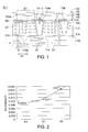
- FIG. 1 shows a cross-sectional view of an LCD device according to an embodiment of the invention
- FIGS. 2-4 show broken line charts illustrating the correlation between the disposition position of a spacer and thickness of the corresponding first electrode according to an embodiment of the invention
- FIG. 5 shows a relative position between a spacer and a light shielding layer of an LCD device according to an embodiment of the invention
- FIG. 6 shows a cross-sectional view of an LCD device according to an embodiment of the invention.
- FIGS. 7-11 show a process flow for manufacturing an LCD device of FIG. 1 .
- FIG. 1 shows a cross-sectional view of an LCD device 10-1 according to an embodiment of the invention.
- the LCD device 10-1 comprises a first substrate 100, a light shielding layer 102, a color filtering layer 104, a first electrode 106, a first alignment layer 108, a main spacer 110a, an auxiliary spacer 110b, a liquid crystal layer 112, a transistor 114, a second electrode 116, a second alignment layer 118 and a second substrate 120.
- the light shielding layer 102 may be disposed on the first substrate 100.
- the light shielding layer 102 can be a black matrix (BM) layer, a metal or non-metal opaque layer, and the light shielding layer 102 has an edge 102a.
- the color filtering layer 104 may be disposed on the light shielding layer 102 for selecting the range of wavelength of the light which could pass through.
- the color filtering layer 104 is a color filter (CF).
- the color filtering layer 104 may selectively comprise a protection layer formed by a polymer such as epoxy resin and acrylic resin for protecting the color filtering layer 104 and enhancing surface smoothness.
- the first electrode 106 may be disposed on the color filtering layer 104.
- the first electrode 106 may be formed by a conductive material.
- the first electrode 106 is a transparent conductive layer formed by such as indium tin oxide (ITO).
- ITO indium tin oxide
- the first electrode 106 has a recess C.
- the shape of the recess C may be semi-circular, step-shaped or any other shapes, and a step-shaped recess C is illustrated for exemplification purpose.
- the recess C has a first thickness H1, the surrounding area of the recess C has a second thickness H2, and the first thickness H1 is smaller than the second thickness H2.
- the main spacer 110a is disposed in the recess C of the first electrode 106 and corresponding to a part of the first electrode 106 having the first thickness H1.
- the auxiliary spacer 110b is disposed on the surrounding area of the recess C of the first electrode 106 and corresponding to a part of the first electrode 106 having the second thickness H2.
- the alignment layer 108 is disposed on a part of the first electrode 106 having the second thickness H2, and is surrounding the sidewall of the main spacer 110a.
- the second substrate 120 has a common electrode E, a main scan line S1, an auxiliary scan line S2 and a transistor 114.
- the transistor 114 is a thin film transistor (TFT).
- the second electrode 116 is disposed on the second substrate 120.
- the second electrode 116 and the first electrode 106 can be formed by the same material.
- the second alignment layer 118 is disposed on the second electrode 116 and the second substrate 120.
- the height of the main spacer 110a is larger than that of the auxiliary spacer 110b.
- the main spacer 110a is mainly used for supporting the stress received between the first substrate 100 and the second substrate 120.
- the disposition of the auxiliary spacer 110b may reduce the space of the liquid crystal layer 112 that needs to be filled with liquid crystal molecules LC, hence reducing the usage amount of liquid crystal molecules LC and avoiding the bubble problem occurring to the liquid crystal layer 112.
- the LCD device 10-1 may be a touch LCD device.
- the auxiliary spacer 110b may prevent the panel of the touch LCD device from being short-circuited when the panel is pressed.
- the main spacer 110a is disposed between the first substrate 100 and the second substrate 120, and the height of the main spacer 110a is exactly equal to the distance from the surface of the recess C of the first electrode 106 to the second alignment layer 118.
- the height of the auxiliary spacer 110b is smaller than the distance from the surface of the first electrode 106 having the second thickness H2 (the peripheral part except the recess C) to the second alignment layer 118.
- the main spacer 110a is disposed in the recess C and is tightly embedded into the recess C.
- the recess C provides the main spacer 110a with a supporting force perpendicular to the first electrode 106 and parallel to the first electrode 106, such that the main spacer 110a can be more firmly fixed on the first electrode 106 and will not be shifted or deformed even when the first substrate 100 and the second substrate 120 respectively receive a stress.
- FIGS. 2-4 show broken line charts illustrating the correlation between the disposition position of a spacer and thickness of the corresponding first electrode according to an embodiment of the invention.
- the vertical axis of the broken line chart which adopts micrometer ( ⁇ m) as unit of measurement, represents the difference between the second thickness H2 and the first thickness H1 of the first electrode 106.
- the horizontal axis of the broken line chart represents the measuring results of the samples K1, K2, and K3.
- the difference between the second thickness H2 and the first thickness H1 of the first electrode 106 must at least be larger than 8nm such that the main spacer 110a (illustrated in FIG. 1 ) can be firmly fixed in the recess C.
- the vertical axis of the broken line chart which adopts micrometer ( ⁇ m) as unit of measurement, represents a ratio of the difference between the second thickness H2 and the first thickness H1 to the second thickness H2.
- the horizontal axis of the broken line chart represents the measuring results of the samples K1, K2, and K3.
- the ratio of the difference between the second thickness H2 and the first thickness H1 to the second thickness H2 must at least be larger than 0.05, such that the main spacer 110a (illustrated in FIG. 1 ) can be firmly fixed in the recess C.
- the vertical axis of the broken line chart which adopts ⁇ m as unit of measurement, represents the ratio of the first thickness H1 to the second thickness H2 of the first electrode 106.
- the horizontal axis of the broken line chart represents the measuring results of the samples K1, K2, and K3.
- the ratio of the first thickness H1 to the second thickness H2 of the first electrode 106 must at least be smaller than 0.95 such that the main spacer 110a (illustrated in FIG. 1 ) can be firmly fixed in the recess C. (illustrated in FIG. 1 ).
- FIG. 5 shows a top view of a spacer and a light shielding layer of an LCD device 10-1 according to an embodiment of the invention.
- the main spacer 110a may be a tapered cylinder, wherein the top surface and the bottom surface may have different diameters.
- the diameter of the top surface may be larger than that of the bottom surface, and the invention is not limited thererto.
- the light shielding layer 102 (slashed area) covers the main spacer 110a and the auxiliary spacer 110b, but the light shielding layer 102 does not cover the pixel unit P.
- the distance R1 is equal to the diameter of the top surface of the main spacer 110a.
- the distance R2 is the width of the light shielding layer 102, such as the distance from the edge 102a to the edge 102b of the light shielding layer 102.
- the LCD device 10-1 of FIG. 1 could be a vertical alignment (VA) LCD device, and the long axis of the liquid crystal molecules LC is perpendicular to the alignment layer 108 and the alignment layer 118.
- VA vertical alignment
- the liquid crystal molecules LC are affected by the electrical field between the first electrode 106 and the second electrode 116 and rotate accordingly. The stronger the electrical field received by the liquid crystal molecules LC, the larger the influence generated on the liquid crystal molecules LC by the electrical field. In other words, the liquid crystal molecules LC are actuated by the alignment layer 108, the alignment layer 118, and the electrical field between the first electrode 106 and the second electrode 116.
- the liquid crystal molecules LC are arranged according to the alignment layer 108 and the alignment layer 118. In an area with stronger electrical field, the liquid crystal molecules LC are mainly affected by the electrical field between the first electrode 106 and the second electrode 116 and are twisted according to the electrical field.
- the liquid crystal molecules LC are affected by the alignment layer 108,118 and the electrical field between the first electrode 106 and the second electrode 116 to move in an irregular manner.
- An unexpected display effect such as wave pattern may easily occur in the unstable area A1. Therefore, the edge 102a of the light shielding layer 102 must be designed to at least cover the unstable area A1.
- the edge 116a of the second electrode 116 is protruded from the edge 102a of the light shielding layer 102 by a protrusion distance R being 1.5 ⁇ m to 10 ⁇ m.
- the size of the light shielding layer 102 determines the aperture ratio of the LCD device 10-1.
- the width of the light shielding layer 102 such as the distance R2 can be reduced to increase the aperture ratio of the LCD device 10-1.
- the distance D1 between the edge 102a or edge 102b 102 and the main spacer 110a is reduced accordingly. Therefore, the distance D1 between the edge 102a and the main spacer 110a is an important parameter in the design of increasing the aperture ratio of the LCD device 10-1 and shielding the unstable area A1 with the light shielding layer 102.
- the distance D1 between the edge 102a of the light shielding layer 102 and the main spacer 110a is at least larger than 5 micrometers ( ⁇ m) and smaller than 26 ⁇ m.
- the distance D1 between the edge 102a and the main spacer 110a is larger than 10 ⁇ m, the light shielding layer 102 is large enough to shield the unstable area A1.
- FIG. 6 a cross-sectional view of an LCD device10-2 according to an embodiment of the invention.
- the LCD device 10-2 comprises a first substrate 100, a light shielding layer 102, a color filtering layer 104, a first electrode 106, a first alignment layer 108, a liquid crystal layer 112, a transistor 114, a second electrode 216, a second alignment layer 218 and a second substrate 120.
- the LCD device 10-2 is similar to the LCD device 10-1 of FIG.1 . Common reference numerals are used throughout the drawings and the detailed description to indicate the same elements, and the similarities are not repeated here.
- the schematic diagrams of the LCD devices 10-1 and 10-2 can be different areas of the same LCD device.
- the LCD device 10-2 has a contact hole H.
- the transistor 114 has a drain electrode D and a source electrode S.
- the second electrode 216 can be electrically connected to the drain electrode D of the transistor 114 through the contact hole H.
- the second alignment layer 218 covers the second electrode 216 and the second substrate 120.
- the arrangement of the liquid crystal molecules LC is affected by the alignment layer 108 and the alignment layer 218, and the liquid crystal molecules LC are affected by the electrical field between the first electrode 106 and the second electrode 216 and rotate accordingly.
- the LCD device 10-2 has a contact hole H, and the second electrode 216 and the alignment layer 218 are disposed above the contact hole H in a manner different from that disposed surrounding the contact hole H.
- An unstable area A2 is formed around the contact hole H and the second electrode 216. Since the liquid crystal molecules LC in the unstable area A2 move in an irregular manner, a non-expected display effect such as wave pattern may easily occur in the unstable area A2. Therefore, the edge 102a of the light shielding layer 102 must at least cover the unstable area A2.
- the distance D2 between an edge 102a of the light shielding layer 102 of the LCD device 10-2 and an edge of the contact hole H at least is larger than 5 ⁇ m and smaller than 26 ⁇ m.
- the distance D2 between the edge 102a and the contact hole H is larger than 10 ⁇ m, the light shielding layer 102 is large enough to shield the unstable area A2. Therefore, the distance D2 between the edge 102a of the light shielding layer 102 and the contact hole H is an important parameter in the design of increasing the aperture ratio of the LCD device 10-2 and shielding the unstable area A2 with the light shielding layer 102.
- FIGS. 7-11 are processes of manufacturing an LCD device 10-1 of FIG. 1 .
- a first substrate 100 is provided, and a light shielding layer 102, a color filtering layer 104 and a conductive material 106' are accordingly formed on the first substrate 100.
- the conductive material 106' can be a transparent conductive material such as indium tin oxide (ITO).
- a photo process is performed for exposure and development processing, and a recess C is formed by an etching process. Then, a first electrode 106 is formed, wherein the first electrode 106 has a first thickness H1 and a second thickness H2, and the second thickness H2 is larger than the first thickness H1.
- the recess C can be circular, rectangular or elliptical, and any shapes would do as long as the recess C can be tightly engaged in conjunction with the top surface of the main spacer 110a (illustrated in FIG. 1 ).
- a main spacer 110a and an auxiliary spacer 110b are formed at the same time by using a mask or a half-tone mask.
- the main spacer 110a is formed in the recess C of the first electrode 106 and corresponding to the first thickness H1.
- the auxiliary spacer 110b is formed in the surrounding area of the recess C of the first electrode 106 and corresponding to the second thickness H2.
- a first alignment layer 108 is formed, wherein the first alignment layer 108 covers the exposed first electrode 106 (the part of the first electrode 106 having the thickness H2), a sidewall of the main spacer 110a, and a sidewall of the auxiliary spacer 110b to form a first plate 12.
- a second plate 14 is provided, wherein the second plate 14 comprises a second electrode 116, a second alignment layer 118 and a second substrate 120.
- the second substrate 120 has a transistor 114, a main scan line S1, an auxiliary scan line S2 and a common electrode E.
- the first plate 12 and the second plate are assembled together.
- Liquid crystal molecules LC are injected between the first substrate 100 and the second substrate 120 to form a liquid crystal layer 112. Then, the manufacturing process of the LCD device 10-1 is completed.
- the main spacer 110a is formed in the recess C after the recess C is formed on the first electrode 106.
- another recess (not illustrated) can be formed on the second electrode 116 for receiving a corresponding main spacer. That is, the main spacer 110a does not have to be embedded in the recess C of the first electrode 106, and any design would do as long as one of the first substrate 100 and the second substrate 120 has a recess for receiving and fixing the main spacer 110a.
- the LCD device 10-1 of FIG. 11 is exemplified by a vertical alignment (VA) LCD device.
- VA vertical alignment
- the design of embedding the main spacer 110a in the recess C according to an embodiment of the invention can also be used in any LCD devices requiring aligning and sealing upper and lower substrates, such as an in-plane switching (IPS) display.
- IPS in-plane switching
- the first electrode has a first thickness and a second thickness, and the second thickness is larger than the first thickness.
- the main spacer is disposed on the part of the first substrate corresponding to the first thickness of the first electrode, such that the main spacer can be tightly engaged through the thickness difference between the first thickness and the second thickness. Therefore, the problem that the first substrate and the second substrate may compress the main spacer after receiving a stress so that the main spacer become shifted and deformed can thus be avoided.
- the range of distance between an edge of the light shielding layer and the main spacer and/or the range of distance between an edge of the light shielding layer and the contact hole can be designed in a manner that the unstable area in which the liquid crystal molecules move irregularly can be shielded even after the width of the light shielding layer is reduced. Therefore, not only increasing the aperture ratio of LCD device but also maintaining the display quality can be achieved.
Landscapes
- Physics & Mathematics (AREA)
- Nonlinear Science (AREA)
- Mathematical Physics (AREA)
- Chemical & Material Sciences (AREA)
- Crystallography & Structural Chemistry (AREA)
- General Physics & Mathematics (AREA)
- Optics & Photonics (AREA)
- Spectroscopy & Molecular Physics (AREA)
- Liquid Crystal (AREA)
Abstract
Description
- The invention relates in general to a display device, and more particularly to a liquid crystal display (LCD) device with spacers.
- With the development of electronic products, electronic devices with a display screen have become popular in everyday life. The liquid crystal display (LCD), being a kind of display screen, normally has two substrates, and a liquid crystal molecule layer is interposed between the two substrates. A plurality of spacers are used for controlling the thickness of the LCD, maintaining a uniform cell gap between upper and lower substrates, and preventing the non-uniform thickness and the response characteristics of liquid crystal molecules from changing, which may result in a blurred display frame.
- In general, reducing the cell gap between upper and lower substrates of an LCD may save the usage amount and increase the response rate of liquid crystal molecules. However, thickness of spacer determines its capacity for receiving stress between upper and lower substrates of the LCD. As the cell gap between two substrates diminishes and makes the thickness of the spacer reduce to such an extent that the spacer can no longer bear the stress of the substrates, the stress may be concentrated on the spacer and further make the spacer deformed or shifted. The disposition of spacers affects the inclination of liquid crystal molecules. The distribution problems of spacers, such as deformation and shifting, will affect the actuation of liquid crystal molecules, and accordingly change the contrast or even the view angle and quality the LCD.
- The disclosure is directed to a liquid crystal display (LCD) device. The electrodes of LCD device have at least have two thickness, and the thickness of the electrode corresponding to the main spacer is smaller than that corresponding to the auxiliary spacer.
- According to an embodiment of the disclosure, a liquid crystal display (LCD) device comprising a first substrate, a first electrode, a second substrate, a liquid crystal layer, a main spacer and an auxiliary spacer is provided. The first electrode is disposed on the first substrate and has a first thickness and a second thickness, wherein the first thickness is smaller than the second thickness. The second substrate and the first substrate are disposed oppositely. The liquid crystal layer is disposed between the first substrate and the second substrate. The main spacer is disposed between the first substrate and the second substrate and corresponding to the part of the first electrode having the first thickness. The auxiliary spacer is disposed between the first substrate and the second substrate and corresponding to the part of the first electrode having the second thickness.
- According to another embodiment of the disclosure, a manufacturing method of LCD device is provided. The method comprises the following steps. A first substrate is provided, wherein a first electrode is disposed on the first substrate and has a first thickness and a second thickness, and the first thickness is smaller than the second thickness. A main spacer is disposed on a part of the first substrate corresponding to the first electrode having the first thickness. An auxiliary spacer is formed on a part of the first substrate corresponding to the second thickness. The first substrate is aligned and sealing with a second substrate. A liquid crystal layer is injected between the first substrate and the second substrate.
- The above and other aspects of the invention will become better understood with regard to the following detailed description of the preferred but non-limiting embodiment(s). The following description is made with reference to the accompanying drawings.
-
FIG. 1 shows a cross-sectional view of an LCD device according to an embodiment of the invention; -
FIGS. 2-4 show broken line charts illustrating the correlation between the disposition position of a spacer and thickness of the corresponding first electrode according to an embodiment of the invention -
FIG. 5 shows a relative position between a spacer and a light shielding layer of an LCD device according to an embodiment of the invention; -
FIG. 6 shows a cross-sectional view of an LCD device according to an embodiment of the invention; -
FIGS. 7-11 show a process flow for manufacturing an LCD device ofFIG. 1 . -
FIG. 1 shows a cross-sectional view of an LCD device 10-1 according to an embodiment of the invention. Referring toFIG. 1 , the LCD device 10-1 comprises afirst substrate 100, alight shielding layer 102, acolor filtering layer 104, afirst electrode 106, afirst alignment layer 108, amain spacer 110a, anauxiliary spacer 110b, aliquid crystal layer 112, atransistor 114, asecond electrode 116, asecond alignment layer 118 and asecond substrate 120. - As indicated in
FIG. 1 , thelight shielding layer 102 may be disposed on thefirst substrate 100. Thelight shielding layer 102 can be a black matrix (BM) layer, a metal or non-metal opaque layer, and thelight shielding layer 102 has anedge 102a. Thecolor filtering layer 104 may be disposed on thelight shielding layer 102 for selecting the range of wavelength of the light which could pass through. Thecolor filtering layer 104 is a color filter (CF). In an embodiment, thecolor filtering layer 104 may selectively comprise a protection layer formed by a polymer such as epoxy resin and acrylic resin for protecting thecolor filtering layer 104 and enhancing surface smoothness. - The
first electrode 106 may be disposed on thecolor filtering layer 104. Thefirst electrode 106 may be formed by a conductive material. Preferably, thefirst electrode 106 is a transparent conductive layer formed by such as indium tin oxide (ITO). Thefirst electrode 106 has a recess C. The shape of the recess C may be semi-circular, step-shaped or any other shapes, and a step-shaped recess C is illustrated for exemplification purpose. The recess C has a first thickness H1, the surrounding area of the recess C has a second thickness H2, and the first thickness H1 is smaller than the second thickness H2. Themain spacer 110a is disposed in the recess C of thefirst electrode 106 and corresponding to a part of thefirst electrode 106 having the first thickness H1. Theauxiliary spacer 110b is disposed on the surrounding area of the recess C of thefirst electrode 106 and corresponding to a part of thefirst electrode 106 having the second thickness H2. Thealignment layer 108 is disposed on a part of thefirst electrode 106 having the second thickness H2, and is surrounding the sidewall of themain spacer 110a. - The
second substrate 120 has a common electrode E, a main scan line S1, an auxiliary scan line S2 and atransistor 114. Thetransistor 114 is a thin film transistor (TFT). Thesecond electrode 116 is disposed on thesecond substrate 120. Thesecond electrode 116 and thefirst electrode 106 can be formed by the same material. Thesecond alignment layer 118 is disposed on thesecond electrode 116 and thesecond substrate 120. - In the present embodiment, the height of the
main spacer 110a is larger than that of theauxiliary spacer 110b. Themain spacer 110a is mainly used for supporting the stress received between thefirst substrate 100 and thesecond substrate 120. The disposition of theauxiliary spacer 110b may reduce the space of theliquid crystal layer 112 that needs to be filled with liquid crystal molecules LC, hence reducing the usage amount of liquid crystal molecules LC and avoiding the bubble problem occurring to theliquid crystal layer 112. In an embodiment, the LCD device 10-1 may be a touch LCD device. Theauxiliary spacer 110b may prevent the panel of the touch LCD device from being short-circuited when the panel is pressed. - As indicated in
FIG. 1 , themain spacer 110a is disposed between thefirst substrate 100 and thesecond substrate 120, and the height of themain spacer 110a is exactly equal to the distance from the surface of the recess C of thefirst electrode 106 to thesecond alignment layer 118. The height of theauxiliary spacer 110b is smaller than the distance from the surface of thefirst electrode 106 having the second thickness H2 (the peripheral part except the recess C) to thesecond alignment layer 118. Themain spacer 110a is disposed in the recess C and is tightly embedded into the recess C. The recess C provides themain spacer 110a with a supporting force perpendicular to thefirst electrode 106 and parallel to thefirst electrode 106, such that themain spacer 110a can be more firmly fixed on thefirst electrode 106 and will not be shifted or deformed even when thefirst substrate 100 and thesecond substrate 120 respectively receive a stress. -
FIGS. 2-4 show broken line charts illustrating the correlation between the disposition position of a spacer and thickness of the corresponding first electrode according to an embodiment of the invention. Referring toFIG. 2 , the vertical axis of the broken line chart, which adopts micrometer (µm) as unit of measurement, represents the difference between the second thickness H2 and the first thickness H1 of thefirst electrode 106. The horizontal axis of the broken line chart represents the measuring results of the samples K1, K2, and K3. As indicated inFIG. 2 , the difference between the second thickness H2 and the first thickness H1 of thefirst electrode 106 must at least be larger than 8nm such that the main spacer 110a (illustrated inFIG. 1 ) can be firmly fixed in the recess C. - Referring to
FIG. 3 , the vertical axis of the broken line chart, which adopts micrometer (µm) as unit of measurement, represents a ratio of the difference between the second thickness H2 and the first thickness H1 to the second thickness H2. The horizontal axis of the broken line chart represents the measuring results of the samples K1, K2, and K3. As indicated inFIG. 3 , the ratio of the difference between the second thickness H2 and the first thickness H1 to the second thickness H2 must at least be larger than 0.05, such that the main spacer 110a (illustrated inFIG. 1 ) can be firmly fixed in the recess C. - Referring to
FIG. 4 . The vertical axis of the broken line chart, which adopts µm as unit of measurement, represents the ratio of the first thickness H1 to the second thickness H2 of thefirst electrode 106. The horizontal axis of the broken line chart represents the measuring results of the samples K1, K2, and K3. As indicated inFIG. 4 , the ratio of the first thickness H1 to the second thickness H2 of thefirst electrode 106 must at least be smaller than 0.95 such that the main spacer 110a (illustrated inFIG. 1 ) can be firmly fixed in the recess C. (illustrated inFIG. 1 ). -
FIG. 5 shows a top view of a spacer and a light shielding layer of an LCD device 10-1 according to an embodiment of the invention. InFIG. 5 , only themain spacer 110a, theauxiliary spacer 110b and thelight shielding layer 102 are illustrated for description purpose. Themain spacer 110a may be a tapered cylinder, wherein the top surface and the bottom surface may have different diameters. For example, the diameter of the top surface may be larger than that of the bottom surface, and the invention is not limited thererto. As indicated inFIG. 5 , the light shielding layer 102 (slashed area) covers themain spacer 110a and theauxiliary spacer 110b, but thelight shielding layer 102 does not cover the pixel unit P. The distance R1 is equal to the diameter of the top surface of themain spacer 110a. The distance R2 is the width of thelight shielding layer 102, such as the distance from theedge 102a to theedge 102b of thelight shielding layer 102. - Referring to
FIG. 1 andFIG. 5 . The LCD device 10-1 ofFIG. 1 could be a vertical alignment (VA) LCD device, and the long axis of the liquid crystal molecules LC is perpendicular to thealignment layer 108 and thealignment layer 118. However, the liquid crystal molecules LC are affected by the electrical field between thefirst electrode 106 and thesecond electrode 116 and rotate accordingly. The stronger the electrical field received by the liquid crystal molecules LC, the larger the influence generated on the liquid crystal molecules LC by the electrical field. In other words, the liquid crystal molecules LC are actuated by thealignment layer 108, thealignment layer 118, and the electrical field between thefirst electrode 106 and thesecond electrode 116. In an area with a weaker electrical field, the liquid crystal molecules LC are arranged according to thealignment layer 108 and thealignment layer 118. In an area with stronger electrical field, the liquid crystal molecules LC are mainly affected by the electrical field between thefirst electrode 106 and thesecond electrode 116 and are twisted according to the electrical field. - In the unstable area A1 between the
alignment layer 108, thealignment layer 118, thefirst electrode 106 and thesecond electrode 116, the liquid crystal molecules LC are affected by the alignment layer 108,118 and the electrical field between thefirst electrode 106 and thesecond electrode 116 to move in an irregular manner. An unexpected display effect such as wave pattern may easily occur in the unstable area A1. Therefore, theedge 102a of thelight shielding layer 102 must be designed to at least cover the unstable area A1. Besides, theedge 116a of thesecond electrode 116 is protruded from theedge 102a of thelight shielding layer 102 by a protrusion distance R being 1.5µm to 10µm. - Referring to
FIG. 1 andFIG. 5 . The size of thelight shielding layer 102 determines the aperture ratio of the LCD device 10-1. In an embodiment, the width of thelight shielding layer 102, such as the distance R2 can be reduced to increase the aperture ratio of the LCD device 10-1. As the distance R2 is reduced, the distance D1 between theedge 102a oredge 102bmain spacer 110a is reduced accordingly. Therefore, the distance D1 between theedge 102a and themain spacer 110a is an important parameter in the design of increasing the aperture ratio of the LCD device 10-1 and shielding the unstable area A1 with thelight shielding layer 102. - In an embodiment of the LCD device 10-1, the distance D1 between the
edge 102a of thelight shielding layer 102 and themain spacer 110a is at least larger than 5 micrometers (µm) and smaller than 26µm. When the distance D1 between theedge 102a and themain spacer 110a is larger than 10µm, thelight shielding layer 102 is large enough to shield the unstable area A1. -
FIG. 6 a cross-sectional view of an LCD device10-2 according to an embodiment of the invention. As indicated inFIG. 6 , the LCD device 10-2 comprises afirst substrate 100, alight shielding layer 102, acolor filtering layer 104, afirst electrode 106, afirst alignment layer 108, aliquid crystal layer 112, atransistor 114, asecond electrode 216, asecond alignment layer 218 and asecond substrate 120. The LCD device 10-2 is similar to the LCD device 10-1 ofFIG.1 . Common reference numerals are used throughout the drawings and the detailed description to indicate the same elements, and the similarities are not repeated here. The schematic diagrams of the LCD devices 10-1 and 10-2 can be different areas of the same LCD device. - The LCD device 10-2 has a contact hole H. The
transistor 114 has a drain electrode D and a source electrode S. Thesecond electrode 216 can be electrically connected to the drain electrode D of thetransistor 114 through the contact hole H. Thesecond alignment layer 218 covers thesecond electrode 216 and thesecond substrate 120. Similarly, the arrangement of the liquid crystal molecules LC is affected by thealignment layer 108 and thealignment layer 218, and the liquid crystal molecules LC are affected by the electrical field between thefirst electrode 106 and thesecond electrode 216 and rotate accordingly. The LCD device 10-2 has a contact hole H, and thesecond electrode 216 and thealignment layer 218 are disposed above the contact hole H in a manner different from that disposed surrounding the contact hole H. An unstable area A2 is formed around the contact hole H and thesecond electrode 216. Since the liquid crystal molecules LC in the unstable area A2 move in an irregular manner, a non-expected display effect such as wave pattern may easily occur in the unstable area A2. Therefore, theedge 102a of thelight shielding layer 102 must at least cover the unstable area A2. - In an embodiment, the distance D2 between an
edge 102a of thelight shielding layer 102 of the LCD device 10-2 and an edge of the contact hole H at least is larger than 5µm and smaller than 26µm. When the distance D2 between theedge 102a and the contact hole H is larger than 10µm, thelight shielding layer 102 is large enough to shield the unstable area A2. Therefore, the distance D2 between theedge 102a of thelight shielding layer 102 and the contact hole H is an important parameter in the design of increasing the aperture ratio of the LCD device 10-2 and shielding the unstable area A2 with thelight shielding layer 102. -
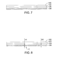
FIGS. 7-11 are processes of manufacturing an LCD device 10-1 ofFIG. 1 . Referring toFIG. 1 . Firstly, afirst substrate 100 is provided, and alight shielding layer 102, acolor filtering layer 104 and a conductive material 106' are accordingly formed on thefirst substrate 100. The conductive material 106' can be a transparent conductive material such as indium tin oxide (ITO). - Referring to
FIG. 8 . A photo process is performed for exposure and development processing, and a recess C is formed by an etching process. Then, afirst electrode 106 is formed, wherein thefirst electrode 106 has a first thickness H1 and a second thickness H2, and the second thickness H2 is larger than the first thickness H1. In the present embodiment, the recess C can be circular, rectangular or elliptical, and any shapes would do as long as the recess C can be tightly engaged in conjunction with the top surface of the main spacer 110a (illustrated inFIG. 1 ). - Referring to
FIG. 9 . Amain spacer 110a and anauxiliary spacer 110b are formed at the same time by using a mask or a half-tone mask. Themain spacer 110a is formed in the recess C of thefirst electrode 106 and corresponding to the first thickness H1. Theauxiliary spacer 110b is formed in the surrounding area of the recess C of thefirst electrode 106 and corresponding to the second thickness H2. - Referring to
FIG. 10 . Afirst alignment layer 108 is formed, wherein thefirst alignment layer 108 covers the exposed first electrode 106 (the part of thefirst electrode 106 having the thickness H2), a sidewall of themain spacer 110a, and a sidewall of theauxiliary spacer 110b to form afirst plate 12. Then, a second plate 14 is provided, wherein the second plate 14 comprises asecond electrode 116, asecond alignment layer 118 and asecond substrate 120. Thesecond substrate 120 has atransistor 114, a main scan line S1, an auxiliary scan line S2 and a common electrode E. Then, thefirst plate 12 and the second plate are assembled together. Referring toFIG. 11 . Liquid crystal molecules LC are injected between thefirst substrate 100 and thesecond substrate 120 to form aliquid crystal layer 112. Then, the manufacturing process of the LCD device 10-1 is completed. - In the manufacturing method of the LCD device 10-1 as indicated in
FIGS. 7-11 , themain spacer 110a is formed in the recess C after the recess C is formed on thefirst electrode 106. In another embodiment, another recess (not illustrated) can be formed on thesecond electrode 116 for receiving a corresponding main spacer. That is, themain spacer 110a does not have to be embedded in the recess C of thefirst electrode 106, and any design would do as long as one of thefirst substrate 100 and thesecond substrate 120 has a recess for receiving and fixing themain spacer 110a. - The LCD device 10-1 of
FIG. 11 is exemplified by a vertical alignment (VA) LCD device. The design of embedding themain spacer 110a in the recess C according to an embodiment of the invention can also be used in any LCD devices requiring aligning and sealing upper and lower substrates, such as an in-plane switching (IPS) display. - An LCD device and a manufacturing method thereof are disclosed in above embodiments of the invention. The first electrode has a first thickness and a second thickness, and the second thickness is larger than the first thickness. The main spacer is disposed on the part of the first substrate corresponding to the first thickness of the first electrode, such that the main spacer can be tightly engaged through the thickness difference between the first thickness and the second thickness. Therefore, the problem that the first substrate and the second substrate may compress the main spacer after receiving a stress so that the main spacer become shifted and deformed can thus be avoided. In some embodiments, the range of distance between an edge of the light shielding layer and the main spacer and/or the range of distance between an edge of the light shielding layer and the contact hole can be designed in a manner that the unstable area in which the liquid crystal molecules move irregularly can be shielded even after the width of the light shielding layer is reduced. Therefore, not only increasing the aperture ratio of LCD device but also maintaining the display quality can be achieved.
- While the invention has been described by way of example and in terms of the preferred embodiment(s), it is to be understood that the invention is not limited thereto. On the contrary, it is intended to cover various modifications and similar arrangements and procedures, and the scope of the appended claims therefore should be accorded the broadest interpretation so as to encompass all such modifications and similar arrangements and procedures.
Claims (15)
- A liquid crystal display (LCD) device, comprising:a first substrate;a first electrode disposed on the first substrate, wherein the first electrode comprises a first thickness and a second thickness, and the first thickness is smaller than the second thickness;a second substrate disposed opposite to the first substrate;a liquid crystal layer disposed between the first substrate and the second substrate;a main spacer disposed between the first substrate and the second substrate and corresponding to a part of the first electrode having the first thickness; andan auxiliary spacer disposed between the first substrate and the second substrate and corresponding to a part of the first electrode having the second thickness.
- The LCD device according to claim 1, wherein a difference between the second thickness and the first thickness is larger than 8nm and smaller than 4µm.
- The LCD device according to claim 1, wherein the ratio of the first thickness to the second thickness is larger than 0.1 and smaller than 0.95.
- The LCD device according to claim 1, wherein the second thickness and the first thickness has a difference, and the ratio of the difference to the second thickness is larger than 0.05 and smaller than 0.2.
- The LCD device according to claim 1, further comprising:a light shielding layer disposed between the first substrate and the first electrode, wherein a smallest distance between an edge of the light shielding layer and a sidewall of the main spacer is between 5µm to 26µm.
- The LCD device according to claim 1, further comprising:a transistor disposed on the second substrate;a second electrode electrically connected to the transistor through a contact hole; anda light shielding layer disposed between the first substrate and the first electrode, wherein the distance between an edge of the light shielding layer and the contact hole is between 5 to 26µm.
- The LCD device according to claim 6, wherein the edge of the second electrode is protruded from the light shielding layer by a protrusion distance being 1.5µm to 10µm.
- The LCD device according to claim 1, further comprising:a second electrode disposed on the second substrate; andan alignment layer disposed on a part of the first electrode having the second thickness, the second electrode and the second substrate and further encapsulating a sidewall of the main spacer.
- The LCD device according to claim 8, wherein the LCD device is a vertical alignment LCD device.
- The LCD device according to claim 1, further comprising:a light shielding layer disposed on the first substrate; anda color filtering layer disposed between the light shielding layer and the first electrode.
- The LCD device according to claim 1, wherein the first electrode has a recess having the first thickness, and a surrounding area of the recess has the second thickness, the main spacer is disposed in the recess and adjacent to the recess, and the recess is separated from an edge of the light shielding layer by 5µm to 26µm.
- The LCD device according to claim 1, wherein a height of the main spacer is larger than a height of the auxiliary spacer.
- A manufacturing method of LCD device, comprising:providing a first substrate, wherein a first electrode is disposed on the first substrate and has a first thickness and a second thickness, and the first thickness is smaller than the second thickness;forming a main spacer on the first substrate corresponding to a part of the first electrode having the first thickness;forming an auxiliary spacer on the first substrate corresponding to the second thickness;aligning and sealing the first substrate with a second substrate; andinjecting a liquid crystal layer between the first substrate and the second substrate.
- The manufacturing method of LCD device according to claim 13, wherein the step of providing the first substrate having the first electrode comprises:providing the first substrate;forming a conductive material on the first substrate; andetching the conductive material to form a recess, wherein the recess has the first thickness, and a surrounding area of the recess has the second thickness.
- The manufacturing method of LCD device according to claim 13, wherein the second substrate has a second electrode and a transistor, the second electrode is electrically connected to the transistor through a contact hole, and before sealing the first substrate with the second substrate, the manufacturing method of LCD device further comprises:forming an alignment layer on a part of the first electrode having the second thickness, the second electrode and the second substrate, and the alignment layer further encapsulating a sidewall of the main spacer.
Priority Applications (1)
| Application Number | Priority Date | Filing Date | Title |
|---|---|---|---|
| EP14168071.0A EP2767866A1 (en) | 2012-10-12 | 2013-10-10 | LCD device and manufacturing method thereof |
Applications Claiming Priority (1)
| Application Number | Priority Date | Filing Date | Title |
|---|---|---|---|
| CN201210387534.5A CN103728786B (en) | 2012-10-12 | 2012-10-12 | Liquid crystal display device and manufacturing method thereof |
Related Child Applications (1)
| Application Number | Title | Priority Date | Filing Date |
|---|---|---|---|
| EP14168071.0A Division EP2767866A1 (en) | 2012-10-12 | 2013-10-10 | LCD device and manufacturing method thereof |
Publications (1)
| Publication Number | Publication Date |
|---|---|
| EP2720081A1 true EP2720081A1 (en) | 2014-04-16 |
Family
ID=49304835
Family Applications (2)
| Application Number | Title | Priority Date | Filing Date |
|---|---|---|---|
| EP14168071.0A Withdrawn EP2767866A1 (en) | 2012-10-12 | 2013-10-10 | LCD device and manufacturing method thereof |
| EP13188016.3A Withdrawn EP2720081A1 (en) | 2012-10-12 | 2013-10-10 | LCD device and manufacturing method thereof |
Family Applications Before (1)
| Application Number | Title | Priority Date | Filing Date |
|---|---|---|---|
| EP14168071.0A Withdrawn EP2767866A1 (en) | 2012-10-12 | 2013-10-10 | LCD device and manufacturing method thereof |
Country Status (3)
| Country | Link |
|---|---|
| US (1) | US9360712B2 (en) |
| EP (2) | EP2767866A1 (en) |
| CN (1) | CN103728786B (en) |
Families Citing this family (12)
| Publication number | Priority date | Publication date | Assignee | Title |
|---|---|---|---|---|
| KR102208432B1 (en) * | 2014-12-31 | 2021-01-27 | 엘지디스플레이 주식회사 | Liquid Crystal Display Device |
| CN104793406A (en) * | 2015-04-29 | 2015-07-22 | 深圳市华星光电技术有限公司 | Liquid crystal display panel and liquid crystal display |
| JP2016224299A (en) * | 2015-06-01 | 2016-12-28 | 株式会社ジャパンディスプレイ | Liquid crystal display device and three-dimensional image display device |
| KR102439841B1 (en) * | 2015-08-31 | 2022-09-01 | 엘지디스플레이 주식회사 | liquid crystal display |
| KR102056595B1 (en) * | 2015-12-17 | 2019-12-17 | 주식회사 엘지화학 | Liquid crystal window and optical member comprising it |
| CN106324932B (en) * | 2016-10-09 | 2019-11-22 | 上海中航光电子有限公司 | Display panel and display device including same |
| JP2019101382A (en) * | 2017-12-08 | 2019-06-24 | シャープ株式会社 | Liquid crystal display device |
| US20190252637A1 (en) * | 2018-02-13 | 2019-08-15 | Innolux Corporation | Foldable display device |
| CN108803108A (en) * | 2018-05-30 | 2018-11-13 | 武汉华星光电技术有限公司 | A kind of touch control LCD (Liquid Crystal Display) panel, display device and terminal |
| CN113946073B (en) * | 2020-06-30 | 2023-06-02 | 京东方科技集团股份有限公司 | Display device and manufacturing method thereof |
| CN112612161B (en) * | 2020-12-11 | 2022-02-18 | 惠科股份有限公司 | Display panel, manufacturing method thereof and display device |
| CN215117092U (en) * | 2021-03-19 | 2021-12-10 | 合肥鑫晟光电科技有限公司 | Liquid crystal display panel and display device |
Citations (2)
| Publication number | Priority date | Publication date | Assignee | Title |
|---|---|---|---|---|
| US20070132920A1 (en) * | 2003-10-22 | 2007-06-14 | Toshiba Matsushita Display Technology Co., Ltd | Liquid crystal display cell |
| US20110222016A1 (en) * | 2010-03-10 | 2011-09-15 | Sony Corporation | Liquid crystal display panel |
Family Cites Families (2)
| Publication number | Priority date | Publication date | Assignee | Title |
|---|---|---|---|---|
| JP3912325B2 (en) * | 2003-05-15 | 2007-05-09 | セイコーエプソン株式会社 | Electro-optical device, electronic apparatus, and method of manufacturing electro-optical device |
| CN101943815A (en) * | 2009-07-07 | 2011-01-12 | 友达光电股份有限公司 | Liquid crystal display device and manufacturing method of electrode substrate thereof |
-
2012
- 2012-10-12 CN CN201210387534.5A patent/CN103728786B/en active Active
-
2013
- 2013-10-08 US US14/048,147 patent/US9360712B2/en active Active
- 2013-10-10 EP EP14168071.0A patent/EP2767866A1/en not_active Withdrawn
- 2013-10-10 EP EP13188016.3A patent/EP2720081A1/en not_active Withdrawn
Patent Citations (2)
| Publication number | Priority date | Publication date | Assignee | Title |
|---|---|---|---|---|
| US20070132920A1 (en) * | 2003-10-22 | 2007-06-14 | Toshiba Matsushita Display Technology Co., Ltd | Liquid crystal display cell |
| US20110222016A1 (en) * | 2010-03-10 | 2011-09-15 | Sony Corporation | Liquid crystal display panel |
Also Published As
| Publication number | Publication date |
|---|---|
| US20140104548A1 (en) | 2014-04-17 |
| EP2767866A1 (en) | 2014-08-20 |
| US9360712B2 (en) | 2016-06-07 |
| CN103728786B (en) | 2016-08-31 |
| CN103728786A (en) | 2014-04-16 |
Similar Documents
| Publication | Publication Date | Title |
|---|---|---|
| US9360712B2 (en) | LCD device and manufacturing method thereof | |
| US10394090B2 (en) | Display panel and manufacture method thereof, display device | |
| KR101357376B1 (en) | Liquid crystal display device | |
| US7643112B2 (en) | Color filter substrate and manufacturing method thereof | |
| US9110336B2 (en) | Liquid crystal display device | |
| US9798194B2 (en) | Liquid crystal display device | |
| US9285637B2 (en) | Liquid-crystal display | |
| CN101285959B (en) | Color filter substrate for liquid crystal display and method of manufacturing same | |
| US20200166795A1 (en) | Manufacturing method for flexible liquid crystal display panel | |
| US10928684B2 (en) | Display device | |
| KR20100025367A (en) | Array substrate, liquid crystal display panel having the same, and method of manufacturing the liquid crystal display panel | |
| CN101750780A (en) | Liquid crystal panel and liquid crystal display device | |
| CN111965906B (en) | Display panel and electronic device | |
| KR20150114393A (en) | Display panel and display device | |
| JP4244289B2 (en) | Substrate for liquid crystal display device and liquid crystal display device including the same | |
| CN107479264A (en) | Display panel and display device | |
| EP2866081A1 (en) | Liquid crystal display panel and liquid crystal display device containing the same | |
| KR101854124B1 (en) | Method of manufacturing polarizing plate, method of manufacturing display apparatus having the same and the display apparatus | |
| CN111948843B (en) | LCD panel | |
| CN112462556A (en) | Display panel | |
| JP2010054552A (en) | Liquid crystal display device | |
| US10895785B2 (en) | Liquid crystal display panel, liquid crystal display panel body component, and method of producing liquid crystal display panels | |
| KR20080058175A (en) | Liquid crystal display device and liquid crystal display device manufacturing method | |
| KR20080061047A (en) | Display device and manufacturing method thereof | |
| CN207337023U (en) | Display panel and display device |
Legal Events
| Date | Code | Title | Description |
|---|---|---|---|
| PUAI | Public reference made under article 153(3) epc to a published international application that has entered the european phase |
Free format text: ORIGINAL CODE: 0009012 |
|
| AK | Designated contracting states |
Kind code of ref document: A1 Designated state(s): AL AT BE BG CH CY CZ DE DK EE ES FI FR GB GR HR HU IE IS IT LI LT LU LV MC MK MT NL NO PL PT RO RS SE SI SK SM TR |
|
| AX | Request for extension of the european patent |
Extension state: BA ME |
|
| 17P | Request for examination filed |
Effective date: 20140604 |
|
| RBV | Designated contracting states (corrected) |
Designated state(s): AL AT BE BG CH CY CZ DE DK EE ES FI FR GB GR HR HU IE IS IT LI LT LU LV MC MK MT NL NO PL PT RO RS SE SI SK SM TR |
|
| 17Q | First examination report despatched |
Effective date: 20160707 |
|
| STAA | Information on the status of an ep patent application or granted ep patent |
Free format text: STATUS: EXAMINATION IS IN PROGRESS |
|
| STAA | Information on the status of an ep patent application or granted ep patent |
Free format text: STATUS: THE APPLICATION IS DEEMED TO BE WITHDRAWN |
|
| 18D | Application deemed to be withdrawn |
Effective date: 20161118 |