EP2717654A1 - Illuminating apparatus and brightness control method - Google Patents
Illuminating apparatus and brightness control method Download PDFInfo
- Publication number
- EP2717654A1 EP2717654A1 EP11866848.2A EP11866848A EP2717654A1 EP 2717654 A1 EP2717654 A1 EP 2717654A1 EP 11866848 A EP11866848 A EP 11866848A EP 2717654 A1 EP2717654 A1 EP 2717654A1
- Authority
- EP
- European Patent Office
- Prior art keywords
- light emitting
- luminance
- emitting elements
- light
- lighting device
- Prior art date
- Legal status (The legal status is an assumption and is not a legal conclusion. Google has not performed a legal analysis and makes no representation as to the accuracy of the status listed.)
- Granted
Links
Images


Classifications
-
- H—ELECTRICITY
- H05—ELECTRIC TECHNIQUES NOT OTHERWISE PROVIDED FOR
- H05B—ELECTRIC HEATING; ELECTRIC LIGHT SOURCES NOT OTHERWISE PROVIDED FOR; CIRCUIT ARRANGEMENTS FOR ELECTRIC LIGHT SOURCES, IN GENERAL
- H05B45/00—Circuit arrangements for operating light-emitting diodes [LED]
- H05B45/20—Controlling the colour of the light
-
- H—ELECTRICITY
- H05—ELECTRIC TECHNIQUES NOT OTHERWISE PROVIDED FOR
- H05B—ELECTRIC HEATING; ELECTRIC LIGHT SOURCES NOT OTHERWISE PROVIDED FOR; CIRCUIT ARRANGEMENTS FOR ELECTRIC LIGHT SOURCES, IN GENERAL
- H05B45/00—Circuit arrangements for operating light-emitting diodes [LED]
- H05B45/40—Details of LED load circuits
- H05B45/44—Details of LED load circuits with an active control inside an LED matrix
-
- H—ELECTRICITY
- H05—ELECTRIC TECHNIQUES NOT OTHERWISE PROVIDED FOR
- H05B—ELECTRIC HEATING; ELECTRIC LIGHT SOURCES NOT OTHERWISE PROVIDED FOR; CIRCUIT ARRANGEMENTS FOR ELECTRIC LIGHT SOURCES, IN GENERAL
- H05B45/00—Circuit arrangements for operating light-emitting diodes [LED]
- H05B45/60—Circuit arrangements for operating LEDs comprising organic material, e.g. for operating organic light-emitting diodes [OLED] or polymer light-emitting diodes [PLED]
-
- H—ELECTRICITY
- H05—ELECTRIC TECHNIQUES NOT OTHERWISE PROVIDED FOR
- H05B—ELECTRIC HEATING; ELECTRIC LIGHT SOURCES NOT OTHERWISE PROVIDED FOR; CIRCUIT ARRANGEMENTS FOR ELECTRIC LIGHT SOURCES, IN GENERAL
- H05B47/00—Circuit arrangements for operating light sources in general, i.e. where the type of light source is not relevant
- H05B47/10—Controlling the light source
- H05B47/155—Coordinated control of two or more light sources
-
- H—ELECTRICITY
- H05—ELECTRIC TECHNIQUES NOT OTHERWISE PROVIDED FOR
- H05B—ELECTRIC HEATING; ELECTRIC LIGHT SOURCES NOT OTHERWISE PROVIDED FOR; CIRCUIT ARRANGEMENTS FOR ELECTRIC LIGHT SOURCES, IN GENERAL
- H05B45/00—Circuit arrangements for operating light-emitting diodes [LED]
- H05B45/50—Circuit arrangements for operating light-emitting diodes [LED] responsive to malfunctions or undesirable behaviour of LEDs; responsive to LED life; Protective circuits
- H05B45/58—Circuit arrangements for operating light-emitting diodes [LED] responsive to malfunctions or undesirable behaviour of LEDs; responsive to LED life; Protective circuits involving end of life detection of LEDs
-
- Y—GENERAL TAGGING OF NEW TECHNOLOGICAL DEVELOPMENTS; GENERAL TAGGING OF CROSS-SECTIONAL TECHNOLOGIES SPANNING OVER SEVERAL SECTIONS OF THE IPC; TECHNICAL SUBJECTS COVERED BY FORMER USPC CROSS-REFERENCE ART COLLECTIONS [XRACs] AND DIGESTS
- Y02—TECHNOLOGIES OR APPLICATIONS FOR MITIGATION OR ADAPTATION AGAINST CLIMATE CHANGE
- Y02B—CLIMATE CHANGE MITIGATION TECHNOLOGIES RELATED TO BUILDINGS, e.g. HOUSING, HOUSE APPLIANCES OR RELATED END-USER APPLICATIONS
- Y02B20/00—Energy efficient lighting technologies, e.g. halogen lamps or gas discharge lamps
- Y02B20/30—Semiconductor lamps, e.g. solid state lamps [SSL] light emitting diodes [LED] or organic LED [OLED]
Definitions
- the present invention relates to a lighting device which comprises a light emitting part including a plurality of light emitting elements and which can adjust luminance and a luminance adjusting method.
- organic EL lighting devices One way to enable organic EL lighting devices to be used in the same way as conventional lighting devices having an electric light bulb or a fluorescent tube as their light emitting source is luminance (brightness) adjustment.
- luminance luminance
- a control part in order to adjust the luminance of the light emitting face, a control part usually adjusts drive voltages applied to, or drive currents flowing through, the organic EL elements according to operation (refer to Patent Literature 1).
- Patent Literature 1 Japanese Patent Application Laid-Open Publication No. 2009-266804
- an object of the present invention is to provide a lighting device and luminance adjusting method which easily enables fine adjustment of luminance in a light-emission mode in which the light emitting part is made to emit light at low luminance.
- a lighting device of the invention according to claim 1 is a lighting device comprising a light emitting part including a plurality of light emitting elements; a luminance setting part setting luminance in a predetermined luminance range; and a control part controlling light emission of the plurality of light emitting elements according to the luminance set by the luminance setting part. If the luminance set by the luminance setting part is less than or equal to threshold luminance that is less than the upper limit of the luminance range, the control part controls a part of light emitting elements of the plurality of light emitting elements not to emit light and intermittently changes the part of light emitting elements in the non-light emission state among the plurality of light emitting elements.
- a luminance adjusting method of the invention according to claim 9 is a luminance adjusting method for a lighting device comprising a light emitting part including a plurality of light emitting elements and comprises a luminance setting step of setting luminance in a predetermined luminance range; and a control step of controlling light emission of the plurality of light emitting elements according to the luminance set by the luminance setting step. If the luminance set by the luminance setting step is less than or equal to threshold luminance that is less than the upper limit of the luminance range, the control step controls a part of light emitting elements of the plurality of light emitting elements not to emit light and intermittently changes the part of light emitting elements in the non-light emission state among the plurality of light emitting elements.
- a light emitting element of the plurality of light emitting elements of the light emitting part is controlled not to emit light so that not all the light emitting elements of the light emitting part are used, that is, light emission is controlled so as to achieve the set luminance by means of light emission of only light emitting elements other than the some light emitting elements.
- fine adjustment of luminance can be easily performed even in a light emission mode in which to make elements emit light at low luminance.
- the light emitting element in the non-light emission state is changed among the plurality of light emitting elements intermittently, degradation progressing in only some light emitting elements is prevented, and thus luminance variation in the regions of the light emitting face can be prevented.
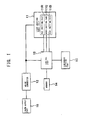
- FIG. 1 shows the configuration of a lighting device that is an embodiment of the present invention.
- This lighting device comprises a color light emitting panel part 11 including organic EL elements as light emitting elements.
- the light emitting panel part 11 has its square light emitting face divided into four equal parts and has four regions 11a to 11d as shown in FIG. 2 .
- This regional division corresponds to the grouping of a plurality of light emitting elements contained in the light emitting panel part 11.
- the four regions 11a to 11d are in a square shape, they may be in another shape such as a triangle or circle and also need not be equally divided parts.
- the light emitting panel part 11 has a structure in which an anode 22, a hole injection layer 23, a hole transporting layer 24, RGB light emitting layers 25R, 25G, 25B, an electron transporting layer 26, and a cathode 27 are laid one over another in that order on a glass substrate 21 as shown in FIG. 3 .
- the anode 22 is constituted by, e.g., an ITO film of 70 nm thickness formed by sputtering.
- the hole injection layer 23 is made of CuPc and 20 nm thick.
- the hole transporting layer 24 is made of NPB and 20 nm thick.
- the R (red) light emitting layer 25R includes CPB as a host material and Ir(phq) 2 tpy as a dopant; the G (green) light emitting layer 25G includes CPB as a host material and Ir(ppy) 3 as a dopant; and the B (blue) light emitting layer 25B includes PAND as a host material and DPAVBi as a dopant.
- the thicknesses of the RGB light emitting layers 25R, 25G, 25B are 40 nm.
- the electron transporting layer 26 is made of NBphen doped with CsxMoOx and 30 nm thick.
- the cathode 27 is constituted by an Al film of 70 to 100 nm thickness. Note that this internal structure of the light emitting panel part 11 is an illustrative example and that the present invention is not limited to this.
- each of the regions 11a to 11d comprises multiple sets of a red light emitting element 11R, a green light emitting element 11G, and a blue light emitting element 11B that are distinguished by the RGB light emitting layers 25R, 25G, 25B.
- the lighting device comprises an AC-DC converter 12, a control part 13, a memory 14, and a luminance setting part 15.
- the AC-DC converter 12 converts an alternating voltage from a power supply part 16 into a direct-current voltage and outputs this.
- the power supply part 16 is, for example, a commercial power supply.
- the output voltage of the AC-DC converter 12 is supplied as a direct-current power supply to the light emitting panel part 11 and the control part 13.
- the control part 13 is constituted by, e.g., a CPU and controls the light emission of the light emitting panel 11 on a region 11a to 11d basis.
- the control of the control part 13 includes luminescent color control as well as luminance control, and the control part 13 can control the red light emitting element 11R, the green light emitting element 11G, and the blue light emitting element 11B individually.
- the memory 14 and the luminance setting part 15 as well as the light emitting panel part 11 are connected to the control part 13.
- the memory 14 stores programs and data necessary for the control of the control part 13.
- the luminance setting part 15 sets the luminance of the entire light emitting panel part 11 according to the operation of a user.
- the luminance can be set at any level within a predetermined luminance range (a lower limit to an upper limit of luminance).
- a power on/off switch for this lighting device may be provided in the luminance setting part 15.
- luminance set by the luminance setting part 15 is hereinafter called set luminance.
- the control part 13 After the luminance of the entire panel is set by the luminance setting part 15, the control part 13 reads the set luminance (step S11) and determines whether or not the set luminance is less than or equal to threshold luminance (step S12).
- the threshold luminance is a luminance within the above luminance range and less than the upper limit of luminance.
- the luminance less than or equal to the threshold luminance is, for example, a luminance in an all-night light mode range. If the set luminance is greater than the threshold luminance, drive current corresponding to the set luminance is supplied to the light emitting elements 11R, 11G, 11B of the four regions 11a to 11d (step S13).
- the light emitting elements 11R, 11G, 11B of all the regions 11a to 11d of the light emitting panel part 11 are driven, and the drive current is controlled such that light emission at the set luminance is obtained from the light emitting elements 11R, 11G, 11B of all those regions 11a to 11d.
- the relations between the set luminance and the respective drive currents of the light emitting elements for the case of driving the light emitting elements of the four regions are stored beforehand as first data in the memory 14 and that the control part 13 controls the drive currents with use of the first data.
- step S14 the regions that were selected at the previous time are read out from the memory 14 (step S14). Then, the regions next to the regions read out at step S14 in order are selected from among the four regions 11a to 11d (step S15).
- the light emitting elements of two regions from among the four regions 11a to 11d are used for light emission.
- the order of region selection is, for example, the order of the regions 11a and 11d and the regions 11b and 11c, which order is repeated.
- the regions 11b and 11c are selected at step S15.
- step S16 After selecting new regions at step S15, the control part 13 starts light emission control for the selected regions (step S16).
- step S16 drive current corresponding to the set luminance of step S13 is supplied to the light emitting elements belonging to the selected two regions.
- the light-emission luminance of the light emitting elements of the selected two regions is controlled to be less than light-emission luminance at the upper limit of luminance. For example, because the light-emission luminance is obtained by multiplying the area of the regions in a light emission state by luminance per unit area, if the relation between the luminance per unit area and the drive current value has been determined, the drive current value corresponding to the set luminance can be decided on for each area of the regions to be in a light emission state.
- the drive current for the light emitting elements 11R, 11G, 11B of the two regions is adjusted such that color temperature becomes 2500 to 3500 K. This adjustment is performed such that the color temperature is, for example, 2500 to 3500 K.
- the drive current is controlled such that light emission at the set luminance is performed by only the light emitting elements 11R, 11G, 11B belonging to the selected two regions.
- the relations between the set luminance and the respective drive currents of the light emitting elements for the case of driving the light emitting elements of the two regions is stored beforehand as second data in the memory 14 and that the control part 13 controls the drive current with use of the second data.
- the control part 13 starts time measurement (step S17) and determines whether the measured time has exceeded a predetermined time (step S18).
- the predetermined time is, for example, three hours, but not being limited to this, may be one hour or six hours or longer. If the measured time has not exceeded the predetermined time, light emission control for the selected regions continues. Although in this embodiment the predetermined time is a fixed time period, it does not have to be a fixed time period.
- control part 13 When determining that the measured time has exceeded the predetermined time, the control part 13 returns to step S15 to select the next regions in order and executes light emission control for the newly selected regions at the next step S16.
- control part 13 resumes the process starting with step S11 by, e.g., an interruption.
- the control part 13 executes this control operation, when in the luminance setting part 15 the set luminance is gradually decreased from the upper limit of luminance within the above luminance range according to the operation of a user, the light emission state of the light emitting panel part 11 can be changed as shown in, e.g., FIG. 5 (a) to (d) . That is, first, when the luminance is set at a luminance within the above luminance range and close to the upper limit of luminance, all the light emitting elements of the regions 11a to 11d emit light at high luminance as shown in FIG. 5 (a) . When the set luminance is decreased to be greater than the threshold luminance, all the light emitting elements of the regions 11a to 11d emit light but at decreased overall luminance as shown in FIG.
- the light emitting elements of the regions 11a and 11d emit light with the light emitting elements of the regions 11b and 11c being in a non-light emission state as shown in FIG. 5 (c) .
- the drive current is controlled such that light emission at the set luminance is obtained with only the light emitting elements 11R, 11G, 11B of the two regions.
- the light emitting elements of the regions 11a and 11d are put in a non-light emission state, and instead the light emitting elements of the regions 11b and 11c emit light as shown in FIG. 5 (d) .
- the light emitting elements of regions in the non-light emission state are replaced with other ones of the light emitting elements of the light emitting panel part 11 each time the predetermined time has elapsed.
- the light emitting elements of the regions 11a to 11d are controlled to emit light in a balanced manner without a state in which only the light emitting elements of a specific region of the light emitting panel part 11 always emit light, and hence the burn-in of only a specific region can be lessened. Further, because the degradation of the light emitting elements of the regions 11a to 11d of the light emitting panel part 11 progresses evenly, luminance deviation and color deviation between the regions of the light emitting panel part 11 can be prevented.
- the lighting device of the above embodiment if the set luminance is less than or equal to the threshold luminance, then only the light emitting elements of some regions of the regions 11a to 11d emit light, and hence the fine adjustment of light-emission luminance in a low luminance range can be easily performed.
- the lighting device of the above embodiment at the same time that only the light emitting elements of some regions of the regions 11a to 11d emit light, by color-toning such that the color temperature of the light emission is 2500 to 3500 K, a light-emission color suitable for use as an all-night light can be obtained.
- surface emission is one of the features of organic EL lighting devices, at bedtime, the smaller lighting area can lessen glare and uncomfortable feeling.
- the light emitting face of the light emitting panel part 11 is divided into the regions 11a to 11d beforehand, the present invention not being limited to this, a single continuous light emitting face may be divided into light emitting elements of regions in the light emission state and light emitting elements of regions in the non-light emission state by the control of the control part 13.
- the light emission state of the light emitting panel part 11 can be changed as shown in FIG. 6 (a) to (d) .
- the light emitting elements of the entire area 31 of the light emitting face of the light emitting panel part 11 emit light at high luminance as shown in FIG. 6 (a) .
- the set luminance is decreased to be greater than the threshold luminance
- the light emitting elements of the entire area 31 emit light but at decreased overall luminance as shown in FIG. 6 (b) .
- the set luminance is further decreased to be less than or equal to the threshold luminance
- the light emitting surface is divided into an area 31a in the light emission state and an area 31b in the non-light emission state by the control of the control part 13.
- the light emitting elements of the area 31a and the light emitting elements of the area 31b in the non-light emission state are controlled separately.
- the drive current is controlled such that light emission at the set luminance is obtained with only the light emitting elements of the area 31a in the light emission state, whereas drive current is not supplied to the light emitting elements of the area 31b in the non-light emission state.
- the light emitting elements in the non-light emission state need only be replaced with other ones of the light emitting elements of the entire area 31 each time the predetermined time has elapsed.
- the light emitting elements in the non-light emission state are replaced, there may be some overlap between the light emitting elements in the non-light emission state before the replacement and the ones in the non-light emission state after the replacement, and in addition the size of the area in the non-light emission state, that is, the number of light emitting elements in the non-light emission state may change between before and after the replacement.
- the drive lifetime is a value at a luminance 30% slower than the upper limit of luminance. It is found out from FIG. 7 that as the color temperature decreases, the luminance ratio of the blue light emitting element having a shorter drive lifetime decreases, whereas that of the red light emitting element having a longer drive lifetime increases. Hence, by color-toning such that the color temperature is 2500 to 3500 K, the lifetime of the light emitting panel part can be made longer, and at the same time, a light-emission color suitable as an all-night light can be obtained as described previously.
- the present invention is not limited to this, other light emitting elements such as LEDs can be used.
- the light emitting part of the present invention may be, for example, a sphere-shaped light emitting part other than a light emitting panel.
- the light-emission color can be adjusted, the light-emission color may be fixed at a predetermined color.
Landscapes
- Electroluminescent Light Sources (AREA)
- Circuit Arrangement For Electric Light Sources In General (AREA)
Abstract
Description
- The present invention relates to a lighting device which comprises a light emitting part including a plurality of light emitting elements and which can adjust luminance and a luminance adjusting method.
- There have been proposed lighting devices which use organic EL (Electro Luminescence) elements as their light emitting source. Lighting devices using organic EL elements (organic EL lighting devices) are characterized by surface emission with no restriction on the shape, and this characteristic cannot be obtained with other lighting devices such as LED lighting devices. Hence, further development for practical use thereof in the future is being expected.
- One way to enable organic EL lighting devices to be used in the same way as conventional lighting devices having an electric light bulb or a fluorescent tube as their light emitting source is luminance (brightness) adjustment. In organic EL lighting devices, in order to adjust the luminance of the light emitting face, a control part usually adjusts drive voltages applied to, or drive currents flowing through, the organic EL elements according to operation (refer to Patent Literature 1).
- Patent Literature 1: Japanese Patent Application Laid-Open Publication No.
2009-266804 - However, with organic EL lighting devices, it is known that as accumulated light-emission time increases, the elements degrade, resulting in a decrease in luminance, and where they are made to emit light at low luminance like so-called all-night lights, there is the problem that it is difficult to finely adjust light-emission luminance to desired low luminance simply by controlling drive voltages or drive currents, because of variation in characteristics of the organic EL elements.
- The above fault can be cited as an example of the problem to be solved by the invention, and an object of the present invention is to provide a lighting device and luminance adjusting method which easily enables fine adjustment of luminance in a light-emission mode in which the light emitting part is made to emit light at low luminance.
- A lighting device of the invention according to claim 1 is a lighting device comprising a light emitting part including a plurality of light emitting elements; a luminance setting part setting luminance in a predetermined luminance range; and a control part controlling light emission of the plurality of light emitting elements according to the luminance set by the luminance setting part. If the luminance set by the luminance setting part is less than or equal to threshold luminance that is less than the upper limit of the luminance range, the control part controls a part of light emitting elements of the plurality of light emitting elements not to emit light and intermittently changes the part of light emitting elements in the non-light emission state among the plurality of light emitting elements.
- A luminance adjusting method of the invention according to claim 9 is a luminance adjusting method for a lighting device comprising a light emitting part including a plurality of light emitting elements and comprises a luminance setting step of setting luminance in a predetermined luminance range; and a control step of controlling light emission of the plurality of light emitting elements according to the luminance set by the luminance setting step. If the luminance set by the luminance setting step is less than or equal to threshold luminance that is less than the upper limit of the luminance range, the control step controls a part of light emitting elements of the plurality of light emitting elements not to emit light and intermittently changes the part of light emitting elements in the non-light emission state among the plurality of light emitting elements.
- According to the lighting device of the invention according to claim 1 and the luminance adjusting method of the invention according to claim 9, if the set luminance is less than or equal to threshold luminance that is less than the upper limit of the luminance range, a light emitting element of the plurality of light emitting elements of the light emitting part is controlled not to emit light so that not all the light emitting elements of the light emitting part are used, that is, light emission is controlled so as to achieve the set luminance by means of light emission of only light emitting elements other than the some light emitting elements. Hence, fine adjustment of luminance can be easily performed even in a light emission mode in which to make elements emit light at low luminance. Further, because the light emitting element in the non-light emission state is changed among the plurality of light emitting elements intermittently, degradation progressing in only some light emitting elements is prevented, and thus luminance variation in the regions of the light emitting face can be prevented.
-
-
FIG. 1 is a block diagram showing the configuration of a lighting device that is an embodiment of the present invention; -
FIG. 2 is a plan view showing the four regions of a light emitting face of the lighting device ofFIG. 1 ; -
FIG. 3 is a cross-sectional view showing the element structure of a light emitting panel part of the lighting device ofFIG. 1 ; -
FIG. 4 is a flow chart showing the control operation of the lighting device ofFIG. 1 ; -
FIG. 5 is a diagram showing example change in the light emission state of the light emitting panel part; -
FIG. 6 is a diagram showing example change in the light emission state of another light emitting panel part; and -
FIG. 7 is a diagram showing the chromaticity, drive lifetimes, and luminance ratios at color temperatures of 5000 K, 3000 K, and 2500 K of a red light emitting element, green light emitting element, and blue light emitting element of the light emitting panel part. - Embodiments of the present invention will be described in detail below with reference to the drawings.
-
FIG. 1 shows the configuration of a lighting device that is an embodiment of the present invention. This lighting device comprises a color lightemitting panel part 11 including organic EL elements as light emitting elements. The lightemitting panel part 11 has its square light emitting face divided into four equal parts and has fourregions 11a to 11d as shown inFIG. 2 . This regional division corresponds to the grouping of a plurality of light emitting elements contained in the lightemitting panel part 11. Although in this embodiment the fourregions 11a to 11d are in a square shape, they may be in another shape such as a triangle or circle and also need not be equally divided parts. - The light
emitting panel part 11 has a structure in which ananode 22, ahole injection layer 23, ahole transporting layer 24, RGBlight emitting layers electron transporting layer 26, and acathode 27 are laid one over another in that order on aglass substrate 21 as shown inFIG. 3 . Theanode 22 is constituted by, e.g., an ITO film of 70 nm thickness formed by sputtering. Thehole injection layer 23 is made of CuPc and 20 nm thick. Thehole transporting layer 24 is made of NPB and 20 nm thick. The R (red)light emitting layer 25R includes CPB as a host material and Ir(phq)2tpy as a dopant; the G (green)light emitting layer 25G includes CPB as a host material and Ir(ppy)3 as a dopant; and the B (blue)light emitting layer 25B includes PAND as a host material and DPAVBi as a dopant. The thicknesses of the RGBlight emitting layers electron transporting layer 26 is made of NBphen doped with CsxMoOx and 30 nm thick. Thecathode 27 is constituted by an Al film of 70 to 100 nm thickness. Note that this internal structure of the lightemitting panel part 11 is an illustrative example and that the present invention is not limited to this. - In the light
emitting panel part 11, each of theregions 11a to 11d comprises multiple sets of a redlight emitting element 11R, a greenlight emitting element 11G, and a bluelight emitting element 11B that are distinguished by the RGBlight emitting layers - The lighting device comprises an AC-
DC converter 12, acontrol part 13, amemory 14, and aluminance setting part 15. The AC-DC converter 12 converts an alternating voltage from apower supply part 16 into a direct-current voltage and outputs this. Thepower supply part 16 is, for example, a commercial power supply. The output voltage of the AC-DC converter 12 is supplied as a direct-current power supply to the lightemitting panel part 11 and thecontrol part 13. Thecontrol part 13 is constituted by, e.g., a CPU and controls the light emission of thelight emitting panel 11 on aregion 11a to 11d basis. The control of thecontrol part 13 includes luminescent color control as well as luminance control, and thecontrol part 13 can control the redlight emitting element 11R, the greenlight emitting element 11G, and the bluelight emitting element 11B individually. - The
memory 14 and theluminance setting part 15 as well as the lightemitting panel part 11 are connected to thecontrol part 13. Thememory 14 stores programs and data necessary for the control of thecontrol part 13. Theluminance setting part 15 sets the luminance of the entire lightemitting panel part 11 according to the operation of a user. In theluminance setting part 15, the luminance can be set at any level within a predetermined luminance range (a lower limit to an upper limit of luminance). A power on/off switch for this lighting device may be provided in theluminance setting part 15. Note that luminance set by theluminance setting part 15 is hereinafter called set luminance. - Next, the control operation of the lighting device having this configuration will be described using the flow chart of
FIG. 4 . - After the luminance of the entire panel is set by the
luminance setting part 15, thecontrol part 13 reads the set luminance (step S11) and determines whether or not the set luminance is less than or equal to threshold luminance (step S12). The threshold luminance is a luminance within the above luminance range and less than the upper limit of luminance. The luminance less than or equal to the threshold luminance is, for example, a luminance in an all-night light mode range. If the set luminance is greater than the threshold luminance, drive current corresponding to the set luminance is supplied to thelight emitting elements regions 11a to 11d (step S13). That is, thelight emitting elements regions 11a to 11d of the lightemitting panel part 11 are driven, and the drive current is controlled such that light emission at the set luminance is obtained from thelight emitting elements regions 11a to 11d. Note that the relations between the set luminance and the respective drive currents of the light emitting elements for the case of driving the light emitting elements of the four regions are stored beforehand as first data in thememory 14 and that thecontrol part 13 controls the drive currents with use of the first data. - In contrast, if the set luminance is less than the threshold luminance, the regions that were selected at the previous time are read out from the memory 14 (step S14). Then, the regions next to the regions read out at step S14 in order are selected from among the four
regions 11a to 11d (step S15). - In the case of light emission at luminance less than or equal to the threshold luminance, the light emitting elements of two regions from among the four
regions 11a to 11d are used for light emission. The order of region selection is, for example, the order of theregions regions regions regions - After selecting new regions at step S15, the
control part 13 starts light emission control for the selected regions (step S16). At step S16, drive current corresponding to the set luminance of step S13 is supplied to the light emitting elements belonging to the selected two regions. The light-emission luminance of the light emitting elements of the selected two regions is controlled to be less than light-emission luminance at the upper limit of luminance. For example, because the light-emission luminance is obtained by multiplying the area of the regions in a light emission state by luminance per unit area, if the relation between the luminance per unit area and the drive current value has been determined, the drive current value corresponding to the set luminance can be decided on for each area of the regions to be in a light emission state. Further, the drive current for thelight emitting elements light emitting elements memory 14 and that thecontrol part 13 controls the drive current with use of the second data. - Then, the
control part 13 starts time measurement (step S17) and determines whether the measured time has exceeded a predetermined time (step S18). The predetermined time is, for example, three hours, but not being limited to this, may be one hour or six hours or longer. If the measured time has not exceeded the predetermined time, light emission control for the selected regions continues. Although in this embodiment the predetermined time is a fixed time period, it does not have to be a fixed time period. - When determining that the measured time has exceeded the predetermined time, the
control part 13 returns to step S15 to select the next regions in order and executes light emission control for the newly selected regions at the next step S16. - If a change to the luminance setting by the
luminance setting part 15 has occurred during the execution of steps S11 to S18, thecontrol part 13 resumes the process starting with step S11 by, e.g., an interruption. - Because the
control part 13 executes this control operation, when in theluminance setting part 15 the set luminance is gradually decreased from the upper limit of luminance within the above luminance range according to the operation of a user, the light emission state of the light emittingpanel part 11 can be changed as shown in, e.g.,FIG. 5 (a) to (d) . That is, first, when the luminance is set at a luminance within the above luminance range and close to the upper limit of luminance, all the light emitting elements of theregions 11a to 11d emit light at high luminance as shown inFIG. 5 (a) . When the set luminance is decreased to be greater than the threshold luminance, all the light emitting elements of theregions 11a to 11d emit light but at decreased overall luminance as shown inFIG. 5 (b) . When the set luminance is further decreased to be less than or equal to the threshold luminance, the light emitting elements of theregions regions FIG. 5 (c) . The drive current is controlled such that light emission at the set luminance is obtained with only thelight emitting elements regions regions FIG. 5 (d) . In other words, the light emitting elements of regions in the non-light emission state are replaced with other ones of the light emitting elements of the light emittingpanel part 11 each time the predetermined time has elapsed. - According to the lighting device of the above embodiment, where the luminance is set to be less than or equal to the threshold luminance, the light emitting elements of the
regions 11a to 11d are controlled to emit light in a balanced manner without a state in which only the light emitting elements of a specific region of the light emittingpanel part 11 always emit light, and hence the burn-in of only a specific region can be lessened. Further, because the degradation of the light emitting elements of theregions 11a to 11d of the light emittingpanel part 11 progresses evenly, luminance deviation and color deviation between the regions of the light emittingpanel part 11 can be prevented. - Further, according to the lighting device of the above embodiment, if the set luminance is less than or equal to the threshold luminance, then only the light emitting elements of some regions of the
regions 11a to 11d emit light, and hence the fine adjustment of light-emission luminance in a low luminance range can be easily performed. - Yet further, according to the lighting device of the above embodiment, at the same time that only the light emitting elements of some regions of the
regions 11a to 11d emit light, by color-toning such that the color temperature of the light emission is 2500 to 3500 K, a light-emission color suitable for use as an all-night light can be obtained. Further, while surface emission is one of the features of organic EL lighting devices, at bedtime, the smaller lighting area can lessen glare and uncomfortable feeling. - Although in the above embodiment the light emitting face of the light emitting
panel part 11 is divided into theregions 11a to 11d beforehand, the present invention not being limited to this, a single continuous light emitting face may be divided into light emitting elements of regions in the light emission state and light emitting elements of regions in the non-light emission state by the control of thecontrol part 13. For example, where the light emitting surface of the light emittingpanel part 11 is not formed being divided into regions beforehand but is a single continuous light emitting face, the light emission state of the light emittingpanel part 11 can be changed as shown inFIG. 6 (a) to (d) . That is, first, when the luminance is set at a luminance within the above luminance range and close to the upper limit of luminance, the light emitting elements of theentire area 31 of the light emitting face of the light emittingpanel part 11 emit light at high luminance as shown inFIG. 6 (a) . When the set luminance is decreased to be greater than the threshold luminance, the light emitting elements of theentire area 31 emit light but at decreased overall luminance as shown inFIG. 6 (b) . When the set luminance is further decreased to be less than or equal to the threshold luminance, the light emitting surface is divided into anarea 31a in the light emission state and anarea 31b in the non-light emission state by the control of thecontrol part 13. That is, the light emitting elements of thearea 31a and the light emitting elements of thearea 31b in the non-light emission state are controlled separately. The drive current is controlled such that light emission at the set luminance is obtained with only the light emitting elements of thearea 31a in the light emission state, whereas drive current is not supplied to the light emitting elements of thearea 31b in the non-light emission state. When a predetermined time has elapsed with the set luminance being maintained less than or equal to the threshold luminance, an area 31c in the light emission state and an area 31d in the non-light emission state, the two areas differing in position from theareas FIG. 6 (d) . As such, in the present invention, the light emitting elements in the non-light emission state need only be replaced with other ones of the light emitting elements of theentire area 31 each time the predetermined time has elapsed. When the light emitting elements in the non-light emission state are replaced, there may be some overlap between the light emitting elements in the non-light emission state before the replacement and the ones in the non-light emission state after the replacement, and in addition the size of the area in the non-light emission state, that is, the number of light emitting elements in the non-light emission state may change between before and after the replacement.FIG. 7 shows the chromaticity, drive lifetimes, and luminance ratios at color temperatures of 5000 K, 3000 K, and 2500 K of the above redlight emitting element 11R, greenlight emitting element 11G, and bluelight emitting element 11B. The drive lifetime is a value at a luminance 30% slower than the upper limit of luminance. It is found out fromFIG. 7 that as the color temperature decreases, the luminance ratio of the blue light emitting element having a shorter drive lifetime decreases, whereas that of the red light emitting element having a longer drive lifetime increases. Hence, by color-toning such that the color temperature is 2500 to 3500 K, the lifetime of the light emitting panel part can be made longer, and at the same time, a light-emission color suitable as an all-night light can be obtained as described previously. - Although in the above embodiments organic EL elements are used as the light emitting elements of the light emitting
panel part 11, the present invention is not limited to this, other light emitting elements such as LEDs can be used. Further, the light emitting part of the present invention may be, for example, a sphere-shaped light emitting part other than a light emitting panel. Although in the above embodiments the light-emission color can be adjusted, the light-emission color may be fixed at a predetermined color. - Reference Signs List
- 11
- Color light emitting panel part
- 12
- AC-DC converter
- 13
- Control part
- 14
- Memory
- 15
- Luminance setting part
- 16
- Power supply part
Claims (9)
- A lighting device comprising a light emitting part including a plurality of light emitting elements; a luminance setting part setting luminance in a predetermined luminance range; and a control part controlling light emission of said plurality of light emitting elements according to the luminance set by said luminance setting part,
wherein if the luminance set by said luminance setting part is less than or equal to threshold luminance that is less than the upper limit of said luminance range, said control part controls a part of light emitting elements of said plurality of light emitting elements not to emit light and intermittently changes said part of light emitting elements in the non-light emission state among said plurality of light emitting elements. - A lighting device according to claim 1, wherein if the luminance set by said luminance setting part is less than or equal to said threshold luminance, said control part controls a light emitting element in a light emission state other than the light emitting elements in said non-light emission state from among said plurality of light emitting elements so as to achieve the luminance set by said luminance setting part by light emission of the light emitting elements in said light emission state.
- A lighting device according to claim 1 or 2, wherein said light emitting part is configured to emit color light, and
wherein if the luminance set by said luminance setting part is less than or equal to said threshold luminance, said control part controls light emitting elements in a light emission state other than the light emitting elements in said non-light emission state from among said plurality of light emitting elements such that light-emission color temperature thereof is 2500 K to 3000 K. - A lighting device according to claim 1 or 2, wherein said plurality of light emitting elements are formed being divided into a plurality of groups, and said control part selects a group to be in said non-light emission state from among said plurality of groups.
- A lighting device according to claim 4, wherein said light emitting part has divided light emitting faces corresponding to said plurality of groups.
- A lighting device according to claim 1 or 2, wherein said light emitting part has a light emitting face formed as a single continuous surface corresponding to said plurality of light emitting elements.
- A lighting device according to claim 1 or 2, Wherein said control part is operative to average frequencies of use of said plurality of light emitting elements by the intermittent replacement of the light emitting elements in said non-light emission state from among said plurality of light emitting elements.
- A lighting device according to any one of claims 1 to 7, wherein said light emitting part comprises a light emitting panel having organic EL elements as said light emitting elements.
- A luminance adjusting method for a lighting device comprising a light emitting part including a plurality of light emitting elements, comprising:a luminance setting step of setting luminance in a predetermined luminance range; anda control step of controlling light emission of said plurality of light emitting elements according to the luminance set by said luminance setting step,wherein if the luminance set by said luminance setting step is less than or equal to threshold luminance that is less than the upper limit of said luminance range, said control step controls a part of light emitting elements of said plurality of light emitting elements not to emit light and intermittently changes said part of light emitting elements in the non-light emission state among said plurality of light emitting elements.
Applications Claiming Priority (1)
| Application Number | Priority Date | Filing Date | Title |
|---|---|---|---|
| PCT/JP2011/062469 WO2012164683A1 (en) | 2011-05-31 | 2011-05-31 | Illuminating apparatus and brightness control method |
Publications (3)
| Publication Number | Publication Date |
|---|---|
| EP2717654A1 true EP2717654A1 (en) | 2014-04-09 |
| EP2717654A4 EP2717654A4 (en) | 2015-09-02 |
| EP2717654B1 EP2717654B1 (en) | 2018-03-07 |
Family
ID=47258569
Family Applications (1)
| Application Number | Title | Priority Date | Filing Date |
|---|---|---|---|
| EP11866848.2A Not-in-force EP2717654B1 (en) | 2011-05-31 | 2011-05-31 | Illuminating apparatus and brightness control method |
Country Status (3)
| Country | Link |
|---|---|
| EP (1) | EP2717654B1 (en) |
| JP (1) | JP5568687B2 (en) |
| WO (1) | WO2012164683A1 (en) |
Families Citing this family (4)
| Publication number | Priority date | Publication date | Assignee | Title |
|---|---|---|---|---|
| WO2014097397A1 (en) * | 2012-12-18 | 2014-06-26 | パイオニア株式会社 | Light-emitting device and method for controlling light-emitting device |
| WO2014097396A1 (en) * | 2012-12-18 | 2014-06-26 | パイオニア株式会社 | Light-emitting device and method for controlling light-emitting device |
| CN105745998A (en) | 2013-10-07 | 2016-07-06 | 飞利浦灯具控股公司 | Drive unit for driving load and drive method |
| JP7204456B2 (en) * | 2018-12-04 | 2023-01-16 | キヤノン株式会社 | Strobe device and its control method and program |
Family Cites Families (5)
| Publication number | Priority date | Publication date | Assignee | Title |
|---|---|---|---|---|
| JP2009266804A (en) | 2008-03-31 | 2009-11-12 | Yamagata Promotional Organization For Industrial Technology | Power feeding device of lighting fixture |
| JP2009289622A (en) * | 2008-05-29 | 2009-12-10 | Sharp Corp | Lighting device |
| JP2010176986A (en) * | 2009-01-28 | 2010-08-12 | Panasonic Electric Works Co Ltd | Color temperature variable lighting system and controller used in same |
| JP5345013B2 (en) * | 2009-07-31 | 2013-11-20 | エーイーテック株式会社 | Interior lighting signboard |
| JP5454029B2 (en) * | 2009-09-10 | 2014-03-26 | セイコーエプソン株式会社 | Lighting device and electronic device |
-
2011
- 2011-05-31 EP EP11866848.2A patent/EP2717654B1/en not_active Not-in-force
- 2011-05-31 WO PCT/JP2011/062469 patent/WO2012164683A1/en not_active Ceased
- 2011-05-31 JP JP2013517743A patent/JP5568687B2/en not_active Expired - Fee Related
Also Published As
| Publication number | Publication date |
|---|---|
| EP2717654A4 (en) | 2015-09-02 |
| JPWO2012164683A1 (en) | 2014-07-31 |
| JP5568687B2 (en) | 2014-08-06 |
| EP2717654B1 (en) | 2018-03-07 |
| WO2012164683A1 (en) | 2012-12-06 |
Similar Documents
| Publication | Publication Date | Title |
|---|---|---|
| EP3122160B1 (en) | Light-emitting device and led light bulb | |
| US9560713B2 (en) | Color tunable light source module with brightness control | |
| JP5620332B2 (en) | System and method for calibrating a solid state lighting panel | |
| TWI455097B (en) | Led selection for white point control in backlights | |
| TW201313071A (en) | Dimmable lighting devices and methods for dimming same | |
| JP2001272938A (en) | Color tone adjustment circuit, backlight module including the circuit, and light emitting diode display device | |
| CN101288341A (en) | Light source emitting mixed-color light and method for controlling chromaticity coordinates of such light source | |
| EP2717654B1 (en) | Illuminating apparatus and brightness control method | |
| CN109346005B (en) | Organic EL panel control device, light source device, organic EL panel control method, program, and recording medium | |
| JP5256623B2 (en) | Lighting device | |
| CN104838726B (en) | Scrolling Interrupt Adjustable Color LED Illumination Source | |
| KR101877195B1 (en) | Method for driving organic electroluminescent element | |
| JP4560494B2 (en) | Operation method of organic light emitting component and organic light emitting component | |
| US11869418B1 (en) | Micro light emitting diode display panel | |
| US8502458B2 (en) | Operating device and method for the combined operation of gas discharge lamps and semiconductor light sources | |
| JPWO2013030980A1 (en) | Lighting device | |
| JP2020030905A (en) | Led light-emitting device | |
| EP3446547B1 (en) | Led driver dimming | |
| JP2021124580A (en) | Liquid crystal display device | |
| TWI795208B (en) | A driving circuit and light-emitting device using the same | |
| US8604720B2 (en) | Light emitting diode driving method | |
| KR20080034294A (en) | Backlight unit and liquid crystal display including the same | |
| CA3020493C (en) | Led driver dimming | |
| WO2013018222A1 (en) | Lighting device and light emission control method for same | |
| JP2018198122A (en) | Light-emitting element and light-emitting device |
Legal Events
| Date | Code | Title | Description |
|---|---|---|---|
| PUAI | Public reference made under article 153(3) epc to a published international application that has entered the european phase |
Free format text: ORIGINAL CODE: 0009012 |
|
| 17P | Request for examination filed |
Effective date: 20131127 |
|
| AK | Designated contracting states |
Kind code of ref document: A1 Designated state(s): AL AT BE BG CH CY CZ DE DK EE ES FI FR GB GR HR HU IE IS IT LI LT LU LV MC MK MT NL NO PL PT RO RS SE SI SK SM TR |
|
| DAX | Request for extension of the european patent (deleted) | ||
| RA4 | Supplementary search report drawn up and despatched (corrected) |
Effective date: 20150805 |
|
| RIC1 | Information provided on ipc code assigned before grant |
Ipc: H05B 37/02 20060101AFI20150730BHEP Ipc: H05B 33/08 20060101ALI20150730BHEP |
|
| RAP1 | Party data changed (applicant data changed or rights of an application transferred) |
Owner name: PIONEER CORPORATION |
|
| GRAP | Despatch of communication of intention to grant a patent |
Free format text: ORIGINAL CODE: EPIDOSNIGR1 |
|
| STAA | Information on the status of an ep patent application or granted ep patent |
Free format text: STATUS: GRANT OF PATENT IS INTENDED |
|
| INTG | Intention to grant announced |
Effective date: 20170922 |
|
| GRAS | Grant fee paid |
Free format text: ORIGINAL CODE: EPIDOSNIGR3 |
|
| GRAA | (expected) grant |
Free format text: ORIGINAL CODE: 0009210 |
|
| STAA | Information on the status of an ep patent application or granted ep patent |
Free format text: STATUS: THE PATENT HAS BEEN GRANTED |
|
| AK | Designated contracting states |
Kind code of ref document: B1 Designated state(s): AL AT BE BG CH CY CZ DE DK EE ES FI FR GB GR HR HU IE IS IT LI LT LU LV MC MK MT NL NO PL PT RO RS SE SI SK SM TR |
|
| REG | Reference to a national code |
Ref country code: GB Ref legal event code: FG4D |
|
| REG | Reference to a national code |
Ref country code: CH Ref legal event code: EP Ref country code: AT Ref legal event code: REF Ref document number: 977910 Country of ref document: AT Kind code of ref document: T Effective date: 20180315 |
|
| REG | Reference to a national code |
Ref country code: DE Ref legal event code: R096 Ref document number: 602011046403 Country of ref document: DE |
|
| REG | Reference to a national code |
Ref country code: IE Ref legal event code: FG4D |
|
| REG | Reference to a national code |
Ref country code: DE Ref legal event code: R084 Ref document number: 602011046403 Country of ref document: DE |
|
| REG | Reference to a national code |
Ref country code: GB Ref legal event code: 746 Effective date: 20180423 |
|
| REG | Reference to a national code |
Ref country code: FR Ref legal event code: PLFP Year of fee payment: 8 |
|
| REG | Reference to a national code |
Ref country code: NL Ref legal event code: MP Effective date: 20180307 |
|
| REG | Reference to a national code |
Ref country code: LT Ref legal event code: MG4D |
|
| PG25 | Lapsed in a contracting state [announced via postgrant information from national office to epo] |
Ref country code: NO Free format text: LAPSE BECAUSE OF FAILURE TO SUBMIT A TRANSLATION OF THE DESCRIPTION OR TO PAY THE FEE WITHIN THE PRESCRIBED TIME-LIMIT Effective date: 20180607 Ref country code: FI Free format text: LAPSE BECAUSE OF FAILURE TO SUBMIT A TRANSLATION OF THE DESCRIPTION OR TO PAY THE FEE WITHIN THE PRESCRIBED TIME-LIMIT Effective date: 20180307 Ref country code: LT Free format text: LAPSE BECAUSE OF FAILURE TO SUBMIT A TRANSLATION OF THE DESCRIPTION OR TO PAY THE FEE WITHIN THE PRESCRIBED TIME-LIMIT Effective date: 20180307 Ref country code: CY Free format text: LAPSE BECAUSE OF FAILURE TO SUBMIT A TRANSLATION OF THE DESCRIPTION OR TO PAY THE FEE WITHIN THE PRESCRIBED TIME-LIMIT Effective date: 20180307 Ref country code: HR Free format text: LAPSE BECAUSE OF FAILURE TO SUBMIT A TRANSLATION OF THE DESCRIPTION OR TO PAY THE FEE WITHIN THE PRESCRIBED TIME-LIMIT Effective date: 20180307 Ref country code: ES Free format text: LAPSE BECAUSE OF FAILURE TO SUBMIT A TRANSLATION OF THE DESCRIPTION OR TO PAY THE FEE WITHIN THE PRESCRIBED TIME-LIMIT Effective date: 20180307 |
|
| REG | Reference to a national code |
Ref country code: AT Ref legal event code: MK05 Ref document number: 977910 Country of ref document: AT Kind code of ref document: T Effective date: 20180307 |
|
| PG25 | Lapsed in a contracting state [announced via postgrant information from national office to epo] |
Ref country code: GR Free format text: LAPSE BECAUSE OF FAILURE TO SUBMIT A TRANSLATION OF THE DESCRIPTION OR TO PAY THE FEE WITHIN THE PRESCRIBED TIME-LIMIT Effective date: 20180608 Ref country code: BG Free format text: LAPSE BECAUSE OF FAILURE TO SUBMIT A TRANSLATION OF THE DESCRIPTION OR TO PAY THE FEE WITHIN THE PRESCRIBED TIME-LIMIT Effective date: 20180607 Ref country code: RS Free format text: LAPSE BECAUSE OF FAILURE TO SUBMIT A TRANSLATION OF THE DESCRIPTION OR TO PAY THE FEE WITHIN THE PRESCRIBED TIME-LIMIT Effective date: 20180307 Ref country code: LV Free format text: LAPSE BECAUSE OF FAILURE TO SUBMIT A TRANSLATION OF THE DESCRIPTION OR TO PAY THE FEE WITHIN THE PRESCRIBED TIME-LIMIT Effective date: 20180307 Ref country code: SE Free format text: LAPSE BECAUSE OF FAILURE TO SUBMIT A TRANSLATION OF THE DESCRIPTION OR TO PAY THE FEE WITHIN THE PRESCRIBED TIME-LIMIT Effective date: 20180307 |
|
| PG25 | Lapsed in a contracting state [announced via postgrant information from national office to epo] |
Ref country code: RO Free format text: LAPSE BECAUSE OF FAILURE TO SUBMIT A TRANSLATION OF THE DESCRIPTION OR TO PAY THE FEE WITHIN THE PRESCRIBED TIME-LIMIT Effective date: 20180307 Ref country code: NL Free format text: LAPSE BECAUSE OF FAILURE TO SUBMIT A TRANSLATION OF THE DESCRIPTION OR TO PAY THE FEE WITHIN THE PRESCRIBED TIME-LIMIT Effective date: 20180307 Ref country code: EE Free format text: LAPSE BECAUSE OF FAILURE TO SUBMIT A TRANSLATION OF THE DESCRIPTION OR TO PAY THE FEE WITHIN THE PRESCRIBED TIME-LIMIT Effective date: 20180307 Ref country code: IT Free format text: LAPSE BECAUSE OF FAILURE TO SUBMIT A TRANSLATION OF THE DESCRIPTION OR TO PAY THE FEE WITHIN THE PRESCRIBED TIME-LIMIT Effective date: 20180307 Ref country code: AL Free format text: LAPSE BECAUSE OF FAILURE TO SUBMIT A TRANSLATION OF THE DESCRIPTION OR TO PAY THE FEE WITHIN THE PRESCRIBED TIME-LIMIT Effective date: 20180307 Ref country code: PL Free format text: LAPSE BECAUSE OF FAILURE TO SUBMIT A TRANSLATION OF THE DESCRIPTION OR TO PAY THE FEE WITHIN THE PRESCRIBED TIME-LIMIT Effective date: 20180307 |
|
| PG25 | Lapsed in a contracting state [announced via postgrant information from national office to epo] |
Ref country code: SK Free format text: LAPSE BECAUSE OF FAILURE TO SUBMIT A TRANSLATION OF THE DESCRIPTION OR TO PAY THE FEE WITHIN THE PRESCRIBED TIME-LIMIT Effective date: 20180307 Ref country code: SM Free format text: LAPSE BECAUSE OF FAILURE TO SUBMIT A TRANSLATION OF THE DESCRIPTION OR TO PAY THE FEE WITHIN THE PRESCRIBED TIME-LIMIT Effective date: 20180307 Ref country code: CZ Free format text: LAPSE BECAUSE OF FAILURE TO SUBMIT A TRANSLATION OF THE DESCRIPTION OR TO PAY THE FEE WITHIN THE PRESCRIBED TIME-LIMIT Effective date: 20180307 Ref country code: AT Free format text: LAPSE BECAUSE OF FAILURE TO SUBMIT A TRANSLATION OF THE DESCRIPTION OR TO PAY THE FEE WITHIN THE PRESCRIBED TIME-LIMIT Effective date: 20180307 |
|
| REG | Reference to a national code |
Ref country code: DE Ref legal event code: R097 Ref document number: 602011046403 Country of ref document: DE |
|
| REG | Reference to a national code |
Ref country code: CH Ref legal event code: PL |
|
| PG25 | Lapsed in a contracting state [announced via postgrant information from national office to epo] |
Ref country code: PT Free format text: LAPSE BECAUSE OF FAILURE TO SUBMIT A TRANSLATION OF THE DESCRIPTION OR TO PAY THE FEE WITHIN THE PRESCRIBED TIME-LIMIT Effective date: 20180709 |
|
| PLBE | No opposition filed within time limit |
Free format text: ORIGINAL CODE: 0009261 |
|
| STAA | Information on the status of an ep patent application or granted ep patent |
Free format text: STATUS: NO OPPOSITION FILED WITHIN TIME LIMIT |
|
| REG | Reference to a national code |
Ref country code: BE Ref legal event code: MM Effective date: 20180531 |
|
| PG25 | Lapsed in a contracting state [announced via postgrant information from national office to epo] |
Ref country code: MC Free format text: LAPSE BECAUSE OF FAILURE TO SUBMIT A TRANSLATION OF THE DESCRIPTION OR TO PAY THE FEE WITHIN THE PRESCRIBED TIME-LIMIT Effective date: 20180307 Ref country code: DK Free format text: LAPSE BECAUSE OF FAILURE TO SUBMIT A TRANSLATION OF THE DESCRIPTION OR TO PAY THE FEE WITHIN THE PRESCRIBED TIME-LIMIT Effective date: 20180307 |
|
| 26N | No opposition filed |
Effective date: 20181210 |
|
| PG25 | Lapsed in a contracting state [announced via postgrant information from national office to epo] |
Ref country code: LI Free format text: LAPSE BECAUSE OF NON-PAYMENT OF DUE FEES Effective date: 20180531 Ref country code: SI Free format text: LAPSE BECAUSE OF FAILURE TO SUBMIT A TRANSLATION OF THE DESCRIPTION OR TO PAY THE FEE WITHIN THE PRESCRIBED TIME-LIMIT Effective date: 20180307 Ref country code: CH Free format text: LAPSE BECAUSE OF NON-PAYMENT OF DUE FEES Effective date: 20180531 |
|
| REG | Reference to a national code |
Ref country code: IE Ref legal event code: MM4A |
|
| PG25 | Lapsed in a contracting state [announced via postgrant information from national office to epo] |
Ref country code: LU Free format text: LAPSE BECAUSE OF NON-PAYMENT OF DUE FEES Effective date: 20180531 |
|
| PG25 | Lapsed in a contracting state [announced via postgrant information from national office to epo] |
Ref country code: IE Free format text: LAPSE BECAUSE OF NON-PAYMENT OF DUE FEES Effective date: 20180531 |
|
| PG25 | Lapsed in a contracting state [announced via postgrant information from national office to epo] |
Ref country code: BE Free format text: LAPSE BECAUSE OF NON-PAYMENT OF DUE FEES Effective date: 20180531 |
|
| PG25 | Lapsed in a contracting state [announced via postgrant information from national office to epo] |
Ref country code: MT Free format text: LAPSE BECAUSE OF NON-PAYMENT OF DUE FEES Effective date: 20180531 |
|
| PG25 | Lapsed in a contracting state [announced via postgrant information from national office to epo] |
Ref country code: TR Free format text: LAPSE BECAUSE OF FAILURE TO SUBMIT A TRANSLATION OF THE DESCRIPTION OR TO PAY THE FEE WITHIN THE PRESCRIBED TIME-LIMIT Effective date: 20180307 |
|
| PG25 | Lapsed in a contracting state [announced via postgrant information from national office to epo] |
Ref country code: HU Free format text: LAPSE BECAUSE OF FAILURE TO SUBMIT A TRANSLATION OF THE DESCRIPTION OR TO PAY THE FEE WITHIN THE PRESCRIBED TIME-LIMIT; INVALID AB INITIO Effective date: 20110531 |
|
| PG25 | Lapsed in a contracting state [announced via postgrant information from national office to epo] |
Ref country code: MK Free format text: LAPSE BECAUSE OF NON-PAYMENT OF DUE FEES Effective date: 20180307 |
|
| PG25 | Lapsed in a contracting state [announced via postgrant information from national office to epo] |
Ref country code: IS Free format text: LAPSE BECAUSE OF FAILURE TO SUBMIT A TRANSLATION OF THE DESCRIPTION OR TO PAY THE FEE WITHIN THE PRESCRIBED TIME-LIMIT Effective date: 20180707 |
|
| REG | Reference to a national code |
Ref country code: FR Ref legal event code: PLFP Year of fee payment: 13 |
|
| PGFP | Annual fee paid to national office [announced via postgrant information from national office to epo] |
Ref country code: FR Payment date: 20240328 Year of fee payment: 14 |
|
| PGFP | Annual fee paid to national office [announced via postgrant information from national office to epo] |
Ref country code: GB Payment date: 20240402 Year of fee payment: 14 |
|
| PGFP | Annual fee paid to national office [announced via postgrant information from national office to epo] |
Ref country code: DE Payment date: 20240328 Year of fee payment: 14 |
|
| REG | Reference to a national code |
Ref country code: DE Ref legal event code: R119 Ref document number: 602011046403 Country of ref document: DE |
|
| GBPC | Gb: european patent ceased through non-payment of renewal fee |
Effective date: 20250531 |
|
| PG25 | Lapsed in a contracting state [announced via postgrant information from national office to epo] |
Ref country code: GB Free format text: LAPSE BECAUSE OF NON-PAYMENT OF DUE FEES Effective date: 20250531 |
|
| PG25 | Lapsed in a contracting state [announced via postgrant information from national office to epo] |
Ref country code: DE Free format text: LAPSE BECAUSE OF NON-PAYMENT OF DUE FEES Effective date: 20251202 |
|
| PG25 | Lapsed in a contracting state [announced via postgrant information from national office to epo] |
Ref country code: FR Free format text: LAPSE BECAUSE OF NON-PAYMENT OF DUE FEES Effective date: 20250531 |