EP2717467A1 - Driver amplifier circuit and power amplifier including the same - Google Patents
Driver amplifier circuit and power amplifier including the same Download PDFInfo
- Publication number
- EP2717467A1 EP2717467A1 EP12275190.2A EP12275190A EP2717467A1 EP 2717467 A1 EP2717467 A1 EP 2717467A1 EP 12275190 A EP12275190 A EP 12275190A EP 2717467 A1 EP2717467 A1 EP 2717467A1
- Authority
- EP
- European Patent Office
- Prior art keywords
- inverter
- output
- delay
- amplifier circuit
- waveform
- Prior art date
- Legal status (The legal status is an assumption and is not a legal conclusion. Google has not performed a legal analysis and makes no representation as to the accuracy of the status listed.)
- Withdrawn
Links
- 238000001914 filtration Methods 0.000 claims abstract description 24
- 230000001934 delay Effects 0.000 claims abstract description 20
- 230000000295 complement effect Effects 0.000 claims description 9
- 229910044991 metal oxide Inorganic materials 0.000 claims description 9
- 150000004706 metal oxides Chemical class 0.000 claims description 9
- 239000004065 semiconductor Substances 0.000 claims description 9
- 230000008878 coupling Effects 0.000 claims description 5
- 238000010168 coupling process Methods 0.000 claims description 5
- 238000005859 coupling reaction Methods 0.000 claims description 5
- 108010075750 P-Type Calcium Channels Proteins 0.000 claims description 3
- 108090000699 N-Type Calcium Channels Proteins 0.000 claims description 2
- 102000004129 N-Type Calcium Channels Human genes 0.000 claims description 2
- 238000007493 shaping process Methods 0.000 claims 2
- 238000010586 diagram Methods 0.000 description 14
- 108091006146 Channels Proteins 0.000 description 3
- 239000000470 constituent Substances 0.000 description 1
- 230000003111 delayed effect Effects 0.000 description 1
- 238000005516 engineering process Methods 0.000 description 1
- 230000004048 modification Effects 0.000 description 1
- 238000012986 modification Methods 0.000 description 1
- 230000003068 static effect Effects 0.000 description 1
Images





Classifications
-
- H—ELECTRICITY
- H03—ELECTRONIC CIRCUITRY
- H03F—AMPLIFIERS
- H03F3/00—Amplifiers with only discharge tubes or only semiconductor devices as amplifying elements
- H03F3/20—Power amplifiers, e.g. Class B amplifiers, Class C amplifiers
- H03F3/21—Power amplifiers, e.g. Class B amplifiers, Class C amplifiers with semiconductor devices only
- H03F3/217—Class D power amplifiers; Switching amplifiers
-
- H—ELECTRICITY
- H03—ELECTRONIC CIRCUITRY
- H03F—AMPLIFIERS
- H03F3/00—Amplifiers with only discharge tubes or only semiconductor devices as amplifying elements
- H03F3/20—Power amplifiers, e.g. Class B amplifiers, Class C amplifiers
-
- H—ELECTRICITY
- H03—ELECTRONIC CIRCUITRY
- H03F—AMPLIFIERS
- H03F1/00—Details of amplifiers with only discharge tubes, only semiconductor devices or only unspecified devices as amplifying elements
- H03F1/32—Modifications of amplifiers to reduce non-linear distortion
-
- H—ELECTRICITY
- H03—ELECTRONIC CIRCUITRY
- H03F—AMPLIFIERS
- H03F3/00—Amplifiers with only discharge tubes or only semiconductor devices as amplifying elements
- H03F3/20—Power amplifiers, e.g. Class B amplifiers, Class C amplifiers
- H03F3/21—Power amplifiers, e.g. Class B amplifiers, Class C amplifiers with semiconductor devices only
- H03F3/217—Class D power amplifiers; Switching amplifiers
- H03F3/2171—Class D power amplifiers; Switching amplifiers with field-effect devices
-
- H—ELECTRICITY
- H03—ELECTRONIC CIRCUITRY
- H03K—PULSE TECHNIQUE
- H03K5/00—Manipulating of pulses not covered by one of the other main groups of this subclass
- H03K5/01—Shaping pulses
Definitions
- the present invention relates to a driver amplifier circuit that may remove a harmonic component using internal resistance of an inverter element, and a power amplifier including the same.
- SOC System On Chip
- a power amplifier In electronic devices, power consumption mainly occurs in analog blocks, and in particular, a power amplifier may be of great importance in the power consumption of analog blocks.
- a power amplifier used for a low power SOC has low output characteristics in comparison with a general power amplifier. Therefore, in light of this, a voltage gain of a driver is generally designed to be high.
- an inverter In recent years, in order to generate a rail-to-rail signal in the driver, an inverter has widely been used. There may be little static power consumption in a structure of the inverter, and therefore, the structure of the inverter has characteristics suitable for a low power structure.
- an output signal may have the characteristics of a square wave, and a large number of harmonic signals may be included in the square wave.
- a separate additional filter may be used, or an inductor may be additionally applied to a load of an output terminal.
- an inductor may be additionally applied to a load of an output terminal.
- An aspect of the present invention provides a driver amplifer circuit capable of having a simplified structure through eliminating a harmonic component using internal resistance of an inverter element, and a power amplifier including the same.
- a driver amplifier circuit including: a filtering unit that shapes an input waveform to have a curved form by using a plurality of invertors connected in parallel; a delay unit that applies different delays to a plurality of respective output waveforms output from the plurality of invertors; and an output unit that overlaps and outputs the plurality of output waveforms to which the different delays are applied by the delay unit, wherein the filtering unit eliminates a harmonic component by using a voltage drop due to internal resistance of the inverter.
- the filtering unit may include an upper inverter connected with a power supply terminal, a lower inverter connected with a ground terminal, a first inverter connected in series with the power supply terminal and the upper inverter, and a second inverter connected in series with the lower inverter and the ground terminal.
- the first and second inverters may output a waveform curved due to the internal resistance occurring between a drain terminal and a source terminal.
- the upper and lower inverters may include a complementary metal oxide semiconductor (CMOS) that forms a complementary coupling.
- CMOS complementary metal oxide semiconductor
- the upper inverter may receive the curved waveform output from the first inverter as a source voltage of a P-type channel metal oxide semiconductor (PMOS).
- PMOS P-type channel metal oxide semiconductor
- the lower inverter may receive the curved waveform output from the second inverter as a source voltage of an n-type channel metal oxide semiconductor (NMOS).
- NMOS n-type channel metal oxide semiconductor
- the delay unit may include an upper delay element that applies a first delay to the output waveform from the upper inverter and a lower delay element that applies a second delay to the output waveform from the lower inverter, and the upper and lower delay elements may have mutually different delay values.
- the delay unit may include a plurality of inverters connected in series.
- the output unit may be an inverter that does not operate complementarily.
- a power amplifier including a driver amplifier circuit
- the driver amplifier circuit includes: a filtering unit that shapes an input waveform to have a curved form by using a plurality of invertors connected in parallel; a delay unit that applies different delays to a plurality of respective output waveforms output from the plurality of invertors; and an output unit that overlaps and outputs the plurality of output waveforms to which the different delays are applied by the delay unit, the filtering unit eliminating a harmonic component by using a voltage drop due to internal resistance of the inverter.
- the filtering unit may include an upper inverter connected with a power supply terminal, a lower inverter connected with a ground terminal, a first inverter connected in series with the power supply terminal and the upper inverter, and a second inverter connected in series with the lower inverter and the ground terminal.
- the first and second inverters may output a waveform curved due to the internal resistance occurring between a drain terminal and a source terminal.
- the upper inverter may include a CMOS that forms a complementary coupling.
- the upper inverter may receive the curved waveform output from the first inverter as a source voltage of a PMOS, and the lower inverter may receive the curved waveform output from the second inverter as a source voltage of an NMOS.
- the delay unit may include an upper delay element that applies a first delay to the output waveform from the upper inverter and a lower delay element that applies a second delay to the output waveform from the lower inverter, and the upper and lower delay elements may have mutually different delay values.
- the delay unit may include a plurality of inverters connected in series.
- the output unit may be an inverter that does not operate complementarily.
- FIG. 1 is a block diagram showing an example of a power amplifier.
- the power amplifier may include a driver amplifier circuit 10, a matching circuit 20, and a load circuit 30.
- a driver amplifier circuit 10 including an inverter may be provided.
- a harmonic component may be eliminated using a voltage drop due to internal resistance of the inverter.
- the present invention does not have a particular limitation to other configurations of the power amplifier except for the driver amplifier circuit 10. Accordingly, particular descriptions of other constituent components will be omitted.
- the power amplifier may be applied to the present invention as long as the power amplifier includes the driver amplifier circuit 10 which will be described below.
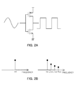
- FIGS. 2A and 2B are reference diagrams showing characteristics of a waveform of an inverter.
- a complementary inverter structure for example, metal oxide semiconductor (MOS)
- MOS metal oxide semiconductor
- FIG. 2B is a graph showing harmonic components of the input and output signals, and as shown in FIG. 2B , it can be seen that the harmonic components are added to the output signal of the inverter to thereby be output as a square wave.
- an additional inverter element may be included therein, and a driver amplifier circuit that eliminates harmonic components by using internal resistance of the additional inverter element may be provided.
- driver amplifier circuit 10 according to an embodiment of the present invention will be described with reference to FIGS. 3 to 8 .
- FIG. 3 is a configuration diagram showing an example of a driver amplifier circuit according to an embodiment of the present invention.
- the driver amplifier circuit 10 may include a filtering unit 100, a delay unit 200, and an output unit 300.
- the filtering unit 100 may shape and output an input waveform. As shown in Fig. 3 , the filtering unit 100 may shape the input waveform to have a curved form by using a plurality of inverters connected in parallel.
- the filtering unit 100 includes an upper inverter 112 and a lower inverter 122 which are respectively connected to an upper portion of the filtering unit 100 and a lower portion thereof will be described, but this is only for the convenience of description, and the present invention is not necessarily limited thereto. That is, according to an embodiment of the present invention, a case in which at least three inverters connected in parallel are used may be applied.
- the filtering unit 100 may include the upper inverter 112 connected with a power supply terminal (Pv), and the lower inverter 122 connected with a ground terminal (Pg).
- the upper inverter 112 and the lower inverter 122 may be implemented as a complementary metal oxide semiconductor (CMOS) that forms a complementary coupling.
- CMOS complementary metal oxide semiconductor
- the filtering unit 100 may further include a first inverter 111 and a second inverter 121.
- the first inverter 111 may be connected in series with the upper inverter 112 and the power supply terminal (Pv)
- the second inverter 121 may be connected in series with the lower inverter 122 and the ground terminal (Pg).
- the filtering unit 100 may eliminate harmonic components using a voltage drop due to internal resistance of the first and second inverters 111 and 121. This will be described in more detail with reference to FIGS. 4 and 5 .
- the delay unit 200 may apply a delay to an output waveform of the filtering unit 100.
- the delay unit 200 may apply different delays to outputs of the plurality of inverters connected in parallel.
- the delay unit 200 may include an upper delay element connected in series with the upper inverter 112 and a lower delay element connected in series with the lower inverter 122.
- the upper delay element may apply a first delay to an output waveform from the upper inverter 112
- the lower delay element may apply a second delay to an output waveform from the lower inverter 122.
- the first and second delays may have different values.
- the delay unit 200 may include a plurality of inverters connected in series.
- the upper and lower delay elements may include different numbers of delays. That is, the number of delays of the upper delay element and the number of delays of the lower delay element may be different, and therefore the first delay value and the second delay value may be differently set.
- the delay unit 200 may output waveforms to which the different first and second delays are applied, and the output unit 300 may overlap the waveforms to which the different first and second delays are applied, thereby effectively eliminating a harmonic wave.
- the output unit 300 may overlap and output a plurality of output waveforms to which different delays are applied by the delay unit 200.
- the output unit 300 may include inverters which are not operated complementarily with each other.
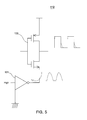
- FIGS. 4 and 5 are reference diagrams showing characteristics of waveforms of first and second inverter units of a driver amplifier circuit according to an embodiment of the present invention.
- the feature in which harmonic components are eliminated using a voltage drop due to internal resistance of the first and second inverters 111 and 121 will be described in detail with reference to FIGS. 4 and 5 .
- FIG. 4 shows characteristics of output waveforms of the first inverter 111 and the upper inverter 112.
- the first inverter 111 may be connected in series between the power supply terminal (Pv) and the upper inverter 112, and may output a predetermined square wave using the internal resistance.
- the first inverter 111 When a low voltage is applied to the first inverter 111, the first inverter 111 may output a waveform curved by internal resistance (RDS) occurring between a drain terminal and a source terminal. That is, when the low voltage is applied to the first inverter 111, a P-type channel metal oxide semiconductor (PMOS) of the first inverter 111 may be turned ON, and therefore the curved waveform may be output by the influence of the internal resistance (channel resistance Rch) occurring between the drain terminal and the source terminal.
- RDS internal resistance
- the upper inverter 112 may receive, as a source voltage of the PMOS, the curved waveform output from the first inverter 111. Accordingly, when a low voltage is applied to the upper inverter 112, the PMOS is turned ON, and therefore a current flows in the PMOS. A voltage drop in the internal resistance of the first inverter 111 is reflected in such a current, and therefore the upper inverter 112 may output a waveform in which a portion of a corner thereof is curved.
- a separate inverter (first inverter) may be added to the power supply terminal (Pv), and a waveform having a curved portion at a corner thereof by using internal resistance (RDS) of the added inverter (first inverter) may be provided.
- Rch internal resistance
- Rch L ⁇ C ox ⁇ W ⁇ V g - V t - V ds / 2
- ⁇ denotes mobility
- Cox denotes a gate oxide capacitance
- W denotes a channel width
- Vg denotes a gate voltage
- Vt denotes a threshold voltage
- Vds denotes a drain-source voltage
- L denotes a channel length.
- FIG. 5 shows characteristics of output waveforms of the second inverter 121 and the lower inverter 122.
- the lower inverter 122 may receive the curved waveform output from the second inverter 121 as a source voltage of an NMOS to thereby output a curved waveform.
- Such an operational principle corresponds to that described in FIG. 4 , and therefore the detailed description thereof will be omitted.
- FIG. 6 is a reference diagram showing characteristics of a waveform of a driver amplifier circuit according to an embodiment of the present invention
- FIG. 7 is a reference diagram showing an output waveform of a driver amplifier circuit according to an embodiment of the present invention.
- a signal having a curved form, different from a square wave may be obtained due to the influence of the first inverter 111, and therefore the output of the upper inverter 112 may be delayed.
- phase of the outputs of the upper and lower inverters 112 and 122 may be provided to be different, and may be penetrated respectively through the PMOS and NMOS of the output unit 300 to thereby be overlapped.
- the inverters of the output unit 300 may not operate complementarily, but may operate in a plurality of sections (four sections in the shown example), and therefore the harmonic components may be eliminated to thereby output signals close to a sine wave.
- FIG. 8 is a reference diagram illustrating characteristics of a waveform based on a delay of a driver amplifier circuit according to an embodiment of the present invention.
- a delay 1 is 1/8
- a delay 2 is 1/4
- a delay 3 is 3/8
- a delay 4 is 1/2
- harmonic components may be eliminated using the internal resistance of the inverter element, whereby the driver amplifier circuit may be simply configured without an additional filter or inductor.
Landscapes
- Engineering & Computer Science (AREA)
- Power Engineering (AREA)
- Physics & Mathematics (AREA)
- Nonlinear Science (AREA)
- Amplifiers (AREA)
Abstract
There are provided a driver amplifier circuit and a power amplifier including the same. The driver amplifier circuit includes a filtering unit that shapes an input waveform to have a curved form by using a plurality of invertors connected in parallel, a delay unit that applies different delays to a plurality of respective output waveforms output from the plurality of invertors, and an output unit that overlaps and outputs the plurality of output waveforms to which the different delays are applied by the delay unit, wherein the filtering unit eliminates a harmonic component by using a voltage drop due to internal resistance of the inverter.
Description
- This application claims the priority of Korean Patent Application No.
10-2012-0111373 filed on October 8, 2012 - The present invention relates to a driver amplifier circuit that may remove a harmonic component using internal resistance of an inverter element, and a power amplifier including the same.
- According to the trend for the miniaturization of electronic devices, a System On Chip (SOC) is used in a variety of electronic devices. In particular, in portable electronic devices, requirements for low SOC power consumption have increased.
- Accordingly, in regard to an SOC, an area thereof, as well as efficiency of power consumption, have emerged as important issues.
- In electronic devices, power consumption mainly occurs in analog blocks, and in particular, a power amplifier may be of great importance in the power consumption of analog blocks. A power amplifier used for a low power SOC has low output characteristics in comparison with a general power amplifier. Therefore, in light of this, a voltage gain of a driver is generally designed to be high.
- In recent years, in order to generate a rail-to-rail signal in the driver, an inverter has widely been used. There may be little static power consumption in a structure of the inverter, and therefore, the structure of the inverter has characteristics suitable for a low power structure.
- However, when configuring the driver using the structure of the inverter, there is a problem in that an output signal may have the characteristics of a square wave, and a large number of harmonic signals may be included in the square wave.
- Accordingly, in order to eliminate the harmonic signals, a separate additional filter may be used, or an inductor may be additionally applied to a load of an output terminal. However, in this case, there is a limitation in that a size of the circuit is increased.
- The following related art documents relate to such existing technology, and still have a limitation in that a separate additional filter or a separate inductor is used so as to eliminate the harmonic signals.
-
- Korean Patent No.
KR 10-1101515 - Korean Patent No.
KR 10-0861797 - An aspect of the present invention provides a driver amplifer circuit capable of having a simplified structure through eliminating a harmonic component using internal resistance of an inverter element, and a power amplifier including the same.
- According to an aspect of the present invention, there is provided a driver amplifier circuit including: a filtering unit that shapes an input waveform to have a curved form by using a plurality of invertors connected in parallel; a delay unit that applies different delays to a plurality of respective output waveforms output from the plurality of invertors; and an output unit that overlaps and outputs the plurality of output waveforms to which the different delays are applied by the delay unit, wherein the filtering unit eliminates a harmonic component by using a voltage drop due to internal resistance of the inverter.
- The filtering unit may include an upper inverter connected with a power supply terminal, a lower inverter connected with a ground terminal, a first inverter connected in series with the power supply terminal and the upper inverter, and a second inverter connected in series with the lower inverter and the ground terminal.
- The first and second inverters may output a waveform curved due to the internal resistance occurring between a drain terminal and a source terminal.
- The upper and lower inverters may include a complementary metal oxide semiconductor (CMOS) that forms a complementary coupling.
- The upper inverter may receive the curved waveform output from the first inverter as a source voltage of a P-type channel metal oxide semiconductor (PMOS).
- The lower inverter may receive the curved waveform output from the second inverter as a source voltage of an n-type channel metal oxide semiconductor (NMOS).
- The delay unit may include an upper delay element that applies a first delay to the output waveform from the upper inverter and a lower delay element that applies a second delay to the output waveform from the lower inverter, and the upper and lower delay elements may have mutually different delay values.
- The delay unit may include a plurality of inverters connected in series.
- The output unit may be an inverter that does not operate complementarily.
- According to another aspect of the present invention, there is provided a power amplifier including a driver amplifier circuit, wherein the driver amplifier circuit includes: a filtering unit that shapes an input waveform to have a curved form by using a plurality of invertors connected in parallel; a delay unit that applies different delays to a plurality of respective output waveforms output from the plurality of invertors; and an output unit that overlaps and outputs the plurality of output waveforms to which the different delays are applied by the delay unit, the filtering unit eliminating a harmonic component by using a voltage drop due to internal resistance of the inverter.
- The filtering unit may include an upper inverter connected with a power supply terminal, a lower inverter connected with a ground terminal, a first inverter connected in series with the power supply terminal and the upper inverter, and a second inverter connected in series with the lower inverter and the ground terminal.
- The first and second inverters may output a waveform curved due to the internal resistance occurring between a drain terminal and a source terminal.
- The upper inverter may include a CMOS that forms a complementary coupling.
- The upper inverter may receive the curved waveform output from the first inverter as a source voltage of a PMOS, and the lower inverter may receive the curved waveform output from the second inverter as a source voltage of an NMOS.
- The delay unit may include an upper delay element that applies a first delay to the output waveform from the upper inverter and a lower delay element that applies a second delay to the output waveform from the lower inverter, and the upper and lower delay elements may have mutually different delay values.
- The delay unit may include a plurality of inverters connected in series.
- The output unit may be an inverter that does not operate complementarily.
- The above and other aspects, features and other advantages of the present invention will be more clearly understood from the following detailed description taken in conjunction with the accompanying drawings, in which:
-
FIG. 1 is a block diagram showing an example of a power amplifier; -
FIGS. 2A and 2B are reference diagrams showing characteristics of a waveform of an inverter; -
FIG. 3 is a circuit diagram showing an example of a driver amplifier circuit according to an embodiment of the present invention; -
FIGS. 4 and5 are reference diagrams showing characteristics of output waveforms of first and second inverter units of a driver amplifier circuit according to an embodiment of the present invention; -
FIG. 6 is a reference diagram showing characteristics of a waveform of a driver amplifier circuit according to an embodiment of the present invention; -
FIG. 7 is a reference diagram showing an output waveform of a driver amplifier circuit according to an embodiment of the present invention; and -
FIG. 8 is a reference diagram illustrating characteristics of a waveform according to a delay of a driver amplifier circuit according to an embodiment of the present invention. - Hereinafter, embodiments of the present invention will be described in detail with reference to the accompanying drawings. The invention may, however, be embodied in many different forms and should not be construed as being limited to the embodiments set forth herein. Rather, these embodiments are provided so that this disclosure will be thorough and complete, and will fully convey the scope of the invention to those skilled in the art.
- In the drawings, the shapes and dimensions of elements may be exaggerated for clarity, and the same reference numerals will be used throughout to designate the same or like elements.
-
FIG. 1 is a block diagram showing an example of a power amplifier. - Referring to
FIG. 1 , the power amplifier may include adriver amplifier circuit 10, amatching circuit 20, and aload circuit 30. - According to the embodiment of the present invention, a
driver amplifier circuit 10 including an inverter may be provided. Particularly, in the embodiment of the present invention, a harmonic component may be eliminated using a voltage drop due to internal resistance of the inverter. - Therefore, the present invention does not have a particular limitation to other configurations of the power amplifier except for the
driver amplifier circuit 10. Accordingly, particular descriptions of other constituent components will be omitted. In addition, even in an embodiment of the power amplifier configured differently from that inFIG. 1 , the power amplifier may be applied to the present invention as long as the power amplifier includes thedriver amplifier circuit 10 which will be described below. -
FIGS. 2A and 2B are reference diagrams showing characteristics of a waveform of an inverter. - As shown in
FIG. 2A , in a complementary inverter structure (for example, metal oxide semiconductor (MOS)), it can be seen that an output signal corresponding to a square wave is output even in a case in which an input signal corresponding to a sine wave is input. -
FIG. 2B is a graph showing harmonic components of the input and output signals, and as shown inFIG. 2B , it can be seen that the harmonic components are added to the output signal of the inverter to thereby be output as a square wave. - In the related art, in order to eliminate the harmonic components of the output signal, a separate additional filter is provided.
- On the other hand, according to an embodiment of the present invention, an additional inverter element may be included therein, and a driver amplifier circuit that eliminates harmonic components by using internal resistance of the additional inverter element may be provided.
- Hereinafter, the
driver amplifier circuit 10 according to an embodiment of the present invention will be described with reference toFIGS. 3 to 8 . -
FIG. 3 is a configuration diagram showing an example of a driver amplifier circuit according to an embodiment of the present invention. - Referring to
FIG. 3 , thedriver amplifier circuit 10 according to an embodiment of the present invention may include afiltering unit 100, adelay unit 200, and anoutput unit 300. - The
filtering unit 100 may shape and output an input waveform. As shown inFig. 3 , thefiltering unit 100 may shape the input waveform to have a curved form by using a plurality of inverters connected in parallel. Hereinafter, an example in which thefiltering unit 100 includes anupper inverter 112 and alower inverter 122 which are respectively connected to an upper portion of thefiltering unit 100 and a lower portion thereof will be described, but this is only for the convenience of description, and the present invention is not necessarily limited thereto. That is, according to an embodiment of the present invention, a case in which at least three inverters connected in parallel are used may be applied. - The
filtering unit 100 may include theupper inverter 112 connected with a power supply terminal (Pv), and thelower inverter 122 connected with a ground terminal (Pg). In an embodiment, theupper inverter 112 and thelower inverter 122 may be implemented as a complementary metal oxide semiconductor (CMOS) that forms a complementary coupling. - The
filtering unit 100 may further include afirst inverter 111 and asecond inverter 121. Here, thefirst inverter 111 may be connected in series with theupper inverter 112 and the power supply terminal (Pv), and thesecond inverter 121 may be connected in series with thelower inverter 122 and the ground terminal (Pg). - The
filtering unit 100 may eliminate harmonic components using a voltage drop due to internal resistance of the first andsecond inverters FIGS. 4 and5 . - The
delay unit 200 may apply a delay to an output waveform of thefiltering unit 100. - In an embodiment, when the
filtering unit 100 includes a plurality of inverters connected in parallel, thedelay unit 200 may apply different delays to outputs of the plurality of inverters connected in parallel. - In an example, the
delay unit 200 may include an upper delay element connected in series with theupper inverter 112 and a lower delay element connected in series with thelower inverter 122. Here, the upper delay element may apply a first delay to an output waveform from theupper inverter 112, and the lower delay element may apply a second delay to an output waveform from thelower inverter 122. Here, the first and second delays may have different values. - The
delay unit 200 may include a plurality of inverters connected in series. - In an example, the upper and lower delay elements may include different numbers of delays. That is, the number of delays of the upper delay element and the number of delays of the lower delay element may be different, and therefore the first delay value and the second delay value may be differently set.
- The
delay unit 200 may output waveforms to which the different first and second delays are applied, and theoutput unit 300 may overlap the waveforms to which the different first and second delays are applied, thereby effectively eliminating a harmonic wave. - The
output unit 300 may overlap and output a plurality of output waveforms to which different delays are applied by thedelay unit 200. - In an embodiment, the
output unit 300 may include inverters which are not operated complementarily with each other. -
FIGS. 4 and5 are reference diagrams showing characteristics of waveforms of first and second inverter units of a driver amplifier circuit according to an embodiment of the present invention. Hereinafter, the feature in which harmonic components are eliminated using a voltage drop due to internal resistance of the first andsecond inverters FIGS. 4 and5 . -
FIG. 4 shows characteristics of output waveforms of thefirst inverter 111 and theupper inverter 112. - The
first inverter 111 may be connected in series between the power supply terminal (Pv) and theupper inverter 112, and may output a predetermined square wave using the internal resistance. - When a low voltage is applied to the
first inverter 111, thefirst inverter 111 may output a waveform curved by internal resistance (RDS) occurring between a drain terminal and a source terminal. That is, when the low voltage is applied to thefirst inverter 111, a P-type channel metal oxide semiconductor (PMOS) of thefirst inverter 111 may be turned ON, and therefore the curved waveform may be output by the influence of the internal resistance (channel resistance Rch) occurring between the drain terminal and the source terminal. - The
upper inverter 112 may receive, as a source voltage of the PMOS, the curved waveform output from thefirst inverter 111. Accordingly, when a low voltage is applied to theupper inverter 112, the PMOS is turned ON, and therefore a current flows in the PMOS. A voltage drop in the internal resistance of thefirst inverter 111 is reflected in such a current, and therefore theupper inverter 112 may output a waveform in which a portion of a corner thereof is curved. - That is, according to the embodiment of the present invention, a separate inverter (first inverter) may be added to the power supply terminal (Pv), and a waveform having a curved portion at a corner thereof by using internal resistance (RDS) of the added inverter (first inverter) may be provided. Such internal resistance Rch may be represented by the following Equation 1.

- Here, "µ" denotes mobility, "Cox" denotes a gate oxide capacitance, "W" denotes a channel width, "Vg" denotes a gate voltage, "Vt" denotes a threshold voltage, "Vds" denotes a drain-source voltage, and "L" denotes a channel length.
-
FIG. 5 shows characteristics of output waveforms of thesecond inverter 121 and thelower inverter 122. - As shown in
FIG. 5 , thelower inverter 122 may receive the curved waveform output from thesecond inverter 121 as a source voltage of an NMOS to thereby output a curved waveform. Such an operational principle corresponds to that described inFIG. 4 , and therefore the detailed description thereof will be omitted. -
FIG. 6 is a reference diagram showing characteristics of a waveform of a driver amplifier circuit according to an embodiment of the present invention, andFIG. 7 is a reference diagram showing an output waveform of a driver amplifier circuit according to an embodiment of the present invention. - As shown in
FIGS. 6 and7 , as an output of theupper inverter 112, a signal having a curved form, different from a square wave, may be obtained due to the influence of thefirst inverter 111, and therefore the output of theupper inverter 112 may be delayed. - As described above, different delays are applied to the outputs of the upper and
lower inverters lower inverters output unit 300 to thereby be overlapped. Here, the inverters of theoutput unit 300 may not operate complementarily, but may operate in a plurality of sections (four sections in the shown example), and therefore the harmonic components may be eliminated to thereby output signals close to a sine wave. -
FIG. 8 is a reference diagram illustrating characteristics of a waveform based on a delay of a driver amplifier circuit according to an embodiment of the present invention. Here, an example in which a delay 1 is 1/8, a delay 2 is 1/4, adelay 3 is 3/8, and adelay 4 is 1/2 is shown. - As shown in
FIG. 8 , more improved performance is shown in the order of thedelays - As set forth above, according to embodiments of the present invention, harmonic components may be eliminated using the internal resistance of the inverter element, whereby the driver amplifier circuit may be simply configured without an additional filter or inductor.
- While the present invention has been shown and described in connection with the embodiments, it will be apparent to those skilled in the art that modifications and variations can be made without departing from the spirit and scope of the invention as defined by the appended claims.
Claims (17)
- A driver amplifier circuit comprising:a filtering unit shaping an input waveform to have a curved form by using a plurality of invertors connected in parallel;a delay unit applying different delays to a plurality of respective output waveforms output from the plurality of invertors; andan output unit overlapping and outputting the plurality of output waveforms to which the different delays are applied by the delay unit,the filtering unit eliminating a harmonic component by using a voltage drop due to internal resistance of the inverter.
- The driver amplifier circuit of claim 1, wherein the filtering unit includes:an upper inverter connected with a power supply terminal;a lower inverter connected with a ground terminal;a first inverter connected in series with the power supply terminal and the upper inverter; anda second inverter connected in series with the lower inverter and the ground terminal.
- The driver amplifier circuit of claim 2, wherein the first and second inverters output a waveform curved due to the internal resistance occurring between a drain terminal and a source terminal.
- The driver amplifier circuit of claim 3, wherein the upper and lower inverters include a complementary metal oxide semiconductor (CMOS) that forms a complementary coupling.
- The driver amplifier circuit of claim 4, wherein the upper inverter receives the curved waveform output from the first inverter as a source voltage of a P-type channel metal oxide semiconductor (PMOS).
- The driver amplifier circuit of claim 4, wherein the lower inverter receives the curved waveform output from the second inverter as a source voltage of a n-type channel metal oxide semiconductor (NMOS).
- The driver amplifier circuit of claim 2, wherein the delay unit includes:an upper delay element that applies a first delay to the output waveform from the upper inverter; anda lower delay element that applies a second delay to the output waveform from the lower inverter, andthe upper and lower delay elements have mutually different delay values.
- The driver amplifier circuit of claim 1, wherein the delay unit includes a plurality of inverters connected in series.
- The driver amplifier circuit of claim 1, wherein the output unit is an inverter that does not operate complementarily.
- A power amplifier comprising a driver amplifier circuit,
the driver amplifier circuit including:a filtering unit shaping an input waveform to have a curved form by using a plurality of invertors connected in parallel;a delay unit applying different delays to a plurality of respective output waveforms output from the plurality of invertors; andan output unit overlapping and outputting the plurality of output waveforms to which the different delays are applied by the delay unit,the filtering unit eliminating a harmonic component by using a voltage drop due to internal resistance of the inverter. - The power amplifier of claim 10, wherein the filtering unit includes:an upper inverter connected with a power supply terminal;a lower inverter connected with a ground terminal;a first inverter connected in series with the power supply terminal and the upper inverter; anda second inverter connected in series with the lower inverter and the ground terminal.
- The power amplifier of claim 11, wherein the first and second inverters output a waveform curved due to the internal resistance occurring between a drain terminal and a source terminal.
- The power amplifier of claim 12, wherein the upper inverter includes a CMOS that forms a complementary coupling.
- The power amplifier of claim 13, wherein the upper inverter receives the curved waveform output from the first inverter as a source voltage of a PMOS, and
the lower inverter receives the curved waveform output from the second inverter as a source voltage of an NMOS. - The power amplifier of claim 11, wherein the delay unit includes:an upper delay element that applies a first delay to the output waveform from the upper inverter; anda lower delay element that applies a second delay to the output waveform from the lower inverter, andthe upper and lower delay elements have mutually different delay values.
- The power amplifier of claim 10, wherein the delay unit includes a plurality of inverters connected in series.
- The power amplifier of claim 10, wherein the output unit is an inverter that does not operate complementarily.
Applications Claiming Priority (1)
| Application Number | Priority Date | Filing Date | Title |
|---|---|---|---|
| KR1020120111373A KR101412949B1 (en) | 2012-10-08 | 2012-10-08 | Driver amplifier circuit and power amplifier using the same |
Publications (1)
| Publication Number | Publication Date |
|---|---|
| EP2717467A1 true EP2717467A1 (en) | 2014-04-09 |
Family
ID=47623882
Family Applications (1)
| Application Number | Title | Priority Date | Filing Date |
|---|---|---|---|
| EP12275190.2A Withdrawn EP2717467A1 (en) | 2012-10-08 | 2012-11-30 | Driver amplifier circuit and power amplifier including the same |
Country Status (2)
| Country | Link |
|---|---|
| EP (1) | EP2717467A1 (en) |
| KR (1) | KR101412949B1 (en) |
Citations (2)
| Publication number | Priority date | Publication date | Assignee | Title |
|---|---|---|---|---|
| US6255867B1 (en) * | 2000-02-23 | 2001-07-03 | Pericom Semiconductor Corp. | CMOS output buffer with feedback control on sources of pre-driver stage |
| US20010026178A1 (en) * | 2000-03-30 | 2001-10-04 | Fujitsu Limited | Output buffer circuit and control method therefor |
Family Cites Families (2)
| Publication number | Priority date | Publication date | Assignee | Title |
|---|---|---|---|---|
| JP3052039B2 (en) * | 1994-07-26 | 2000-06-12 | 日本プレシジョン・サーキッツ株式会社 | Input amplifier circuit |
| JP4351882B2 (en) * | 2003-08-19 | 2009-10-28 | 新日本無線株式会社 | Digital power amplifier |
-
2012
- 2012-10-08 KR KR1020120111373A patent/KR101412949B1/en not_active Expired - Fee Related
- 2012-11-30 EP EP12275190.2A patent/EP2717467A1/en not_active Withdrawn
Patent Citations (2)
| Publication number | Priority date | Publication date | Assignee | Title |
|---|---|---|---|---|
| US6255867B1 (en) * | 2000-02-23 | 2001-07-03 | Pericom Semiconductor Corp. | CMOS output buffer with feedback control on sources of pre-driver stage |
| US20010026178A1 (en) * | 2000-03-30 | 2001-10-04 | Fujitsu Limited | Output buffer circuit and control method therefor |
Also Published As
| Publication number | Publication date |
|---|---|
| KR20140045165A (en) | 2014-04-16 |
| KR101412949B1 (en) | 2014-06-26 |
Similar Documents
| Publication | Publication Date | Title |
|---|---|---|
| CN106941317B (en) | Charge pump unit and charge pump circuit | |
| CN104518776B (en) | Level shifter of driving circuit and operation method thereof | |
| US9893729B2 (en) | Level shifter of driving circuit | |
| JP6289974B2 (en) | Semiconductor device | |
| US10483954B2 (en) | Clock generation circuit and charge pumping system | |
| CN103178709B (en) | Charge pump circuit and sequential control method thereof | |
| US20130257522A1 (en) | High input voltage charge pump | |
| US9948302B2 (en) | Level shift circuit | |
| US10236876B2 (en) | Switch control circuit with booster | |
| US8975927B2 (en) | Gate driver | |
| KR101538157B1 (en) | Voltage level converor and rf switching driver apparatus using the same | |
| US9472951B2 (en) | Electrostatic discharge protection device and integrated circuit using same | |
| US9882435B2 (en) | Resonant type high frequency power supply device and switching circuit for resonant type high frequency power supply device | |
| CN110838847A (en) | Dynamic comparator and control method thereof | |
| CN107395012B (en) | Charge pump circuit and control method thereof | |
| US20120306561A1 (en) | I/o circuit and integrated circuit | |
| CN104919703A (en) | Single-ended high voltage input-capable comparator circuit | |
| Calvillo-Cortes et al. | A 65nm CMOS pulse-width-controlled driver with 8V pp output voltage for switch-mode RF PAs up to 3.6 GHz | |
| CN108781071B (en) | Square wave generating method and square wave generating circuit | |
| CN103106921B (en) | Level displacement shifter for row decoding circuit | |
| KR101412949B1 (en) | Driver amplifier circuit and power amplifier using the same | |
| TWI493855B (en) | Voltage converter | |
| US9882509B2 (en) | Resonant type high frequency power supply device and switching circuit for resonant type high frequency power supply device | |
| US8354874B1 (en) | Kickback cancellation in class B type circuits using AC coupling | |
| CN205725660U (en) | power drive circuit |
Legal Events
| Date | Code | Title | Description |
|---|---|---|---|
| PUAI | Public reference made under article 153(3) epc to a published international application that has entered the european phase |
Free format text: ORIGINAL CODE: 0009012 |
|
| 17P | Request for examination filed |
Effective date: 20121130 |
|
| AK | Designated contracting states |
Kind code of ref document: A1 Designated state(s): AL AT BE BG CH CY CZ DE DK EE ES FI FR GB GR HR HU IE IS IT LI LT LU LV MC MK MT NL NO PL PT RO RS SE SI SK SM TR |
|
| AX | Request for extension of the european patent |
Extension state: BA ME |
|
| STAA | Information on the status of an ep patent application or granted ep patent |
Free format text: STATUS: THE APPLICATION HAS BEEN WITHDRAWN |
|
| 18W | Application withdrawn |
Effective date: 20160203 |