EP2717457B1 - Power conversion device - Google Patents
Power conversion device Download PDFInfo
- Publication number
- EP2717457B1 EP2717457B1 EP12793891.8A EP12793891A EP2717457B1 EP 2717457 B1 EP2717457 B1 EP 2717457B1 EP 12793891 A EP12793891 A EP 12793891A EP 2717457 B1 EP2717457 B1 EP 2717457B1
- Authority
- EP
- European Patent Office
- Prior art keywords
- switching devices
- bidirectional switching
- power conversion
- busbars
- conversion apparatus
- Prior art date
- Legal status (The legal status is an assumption and is not a legal conclusion. Google has not performed a legal analysis and makes no representation as to the accuracy of the status listed.)
- Active
Links
Images


Classifications
-
- H—ELECTRICITY
- H02—GENERATION; CONVERSION OR DISTRIBUTION OF ELECTRIC POWER
- H02M—APPARATUS FOR CONVERSION BETWEEN AC AND AC, BETWEEN AC AND DC, OR BETWEEN DC AND DC, AND FOR USE WITH MAINS OR SIMILAR POWER SUPPLY SYSTEMS; CONVERSION OF DC OR AC INPUT POWER INTO SURGE OUTPUT POWER; CONTROL OR REGULATION THEREOF
- H02M5/00—Conversion of ac power input into ac power output, e.g. for change of voltage, for change of frequency, for change of number of phases
- H02M5/02—Conversion of ac power input into ac power output, e.g. for change of voltage, for change of frequency, for change of number of phases without intermediate conversion into dc
- H02M5/04—Conversion of ac power input into ac power output, e.g. for change of voltage, for change of frequency, for change of number of phases without intermediate conversion into dc by static converters
- H02M5/22—Conversion of ac power input into ac power output, e.g. for change of voltage, for change of frequency, for change of number of phases without intermediate conversion into dc by static converters using discharge tubes with control electrode or semiconductor devices with control electrode
- H02M5/275—Conversion of ac power input into ac power output, e.g. for change of voltage, for change of frequency, for change of number of phases without intermediate conversion into dc by static converters using discharge tubes with control electrode or semiconductor devices with control electrode using devices of a triode or transistor type requiring continuous application of a control signal
- H02M5/293—Conversion of ac power input into ac power output, e.g. for change of voltage, for change of frequency, for change of number of phases without intermediate conversion into dc by static converters using discharge tubes with control electrode or semiconductor devices with control electrode using devices of a triode or transistor type requiring continuous application of a control signal using semiconductor devices only
-
- H—ELECTRICITY
- H02—GENERATION; CONVERSION OR DISTRIBUTION OF ELECTRIC POWER
- H02M—APPARATUS FOR CONVERSION BETWEEN AC AND AC, BETWEEN AC AND DC, OR BETWEEN DC AND DC, AND FOR USE WITH MAINS OR SIMILAR POWER SUPPLY SYSTEMS; CONVERSION OF DC OR AC INPUT POWER INTO SURGE OUTPUT POWER; CONTROL OR REGULATION THEREOF
- H02M7/00—Conversion of ac power input into dc power output; Conversion of dc power input into ac power output
- H02M7/003—Constructional details, e.g. physical layout, assembly, wiring or busbar connections
-
- H—ELECTRICITY
- H05—ELECTRIC TECHNIQUES NOT OTHERWISE PROVIDED FOR
- H05K—PRINTED CIRCUITS; CASINGS OR CONSTRUCTIONAL DETAILS OF ELECTRIC APPARATUS; MANUFACTURE OF ASSEMBLAGES OF ELECTRICAL COMPONENTS
- H05K7/00—Constructional details common to different types of electric apparatus
- H05K7/14—Mounting supporting structure in casing or on frame or rack
- H05K7/1422—Printed circuit boards receptacles, e.g. stacked structures, electronic circuit modules or box like frames
- H05K7/1427—Housings
- H05K7/1432—Housings specially adapted for power drive units or power converters
- H05K7/14329—Housings specially adapted for power drive units or power converters specially adapted for the configuration of power bus bars
-
- G—PHYSICS
- G01—MEASURING; TESTING
- G01R—MEASURING ELECTRIC VARIABLES; MEASURING MAGNETIC VARIABLES
- G01R25/00—Arrangements for measuring phase angle between a voltage and a current or between voltages or currents
-
- G—PHYSICS
- G01—MEASURING; TESTING
- G01R—MEASURING ELECTRIC VARIABLES; MEASURING MAGNETIC VARIABLES
- G01R35/00—Testing or calibrating of apparatus covered by the other groups of this subclass
-
- G—PHYSICS
- G01—MEASURING; TESTING
- G01R—MEASURING ELECTRIC VARIABLES; MEASURING MAGNETIC VARIABLES
- G01R35/00—Testing or calibrating of apparatus covered by the other groups of this subclass
- G01R35/005—Calibrating; Standards or reference devices, e.g. voltage or resistance standards, "golden" references
-
- H—ELECTRICITY
- H01—ELECTRIC ELEMENTS
- H01F—MAGNETS; INDUCTANCES; TRANSFORMERS; SELECTION OF MATERIALS FOR THEIR MAGNETIC PROPERTIES
- H01F30/00—Fixed transformers not covered by group H01F19/00
- H01F30/06—Fixed transformers not covered by group H01F19/00 characterised by the structure
- H01F30/12—Two-phase, three-phase or polyphase transformers
- H01F30/14—Two-phase, three-phase or polyphase transformers for changing the number of phases
-
- H—ELECTRICITY
- H02—GENERATION; CONVERSION OR DISTRIBUTION OF ELECTRIC POWER
- H02M—APPARATUS FOR CONVERSION BETWEEN AC AND AC, BETWEEN AC AND DC, OR BETWEEN DC AND DC, AND FOR USE WITH MAINS OR SIMILAR POWER SUPPLY SYSTEMS; CONVERSION OF DC OR AC INPUT POWER INTO SURGE OUTPUT POWER; CONTROL OR REGULATION THEREOF
- H02M1/00—Details of apparatus for conversion
- H02M1/42—Circuits or arrangements for compensating for or adjusting power factor in converters or inverters
- H02M1/4208—Arrangements for improving power factor of AC input
- H02M1/4258—Arrangements for improving power factor of AC input using a single converter stage both for correction of AC input power factor and generation of a regulated and galvanically isolated DC output voltage
-
- H—ELECTRICITY
- H02—GENERATION; CONVERSION OR DISTRIBUTION OF ELECTRIC POWER
- H02M—APPARATUS FOR CONVERSION BETWEEN AC AND AC, BETWEEN AC AND DC, OR BETWEEN DC AND DC, AND FOR USE WITH MAINS OR SIMILAR POWER SUPPLY SYSTEMS; CONVERSION OF DC OR AC INPUT POWER INTO SURGE OUTPUT POWER; CONTROL OR REGULATION THEREOF
- H02M5/00—Conversion of ac power input into ac power output, e.g. for change of voltage, for change of frequency, for change of number of phases
- H02M5/02—Conversion of ac power input into ac power output, e.g. for change of voltage, for change of frequency, for change of number of phases without intermediate conversion into dc
- H02M5/04—Conversion of ac power input into ac power output, e.g. for change of voltage, for change of frequency, for change of number of phases without intermediate conversion into dc by static converters
- H02M5/10—Conversion of ac power input into ac power output, e.g. for change of voltage, for change of frequency, for change of number of phases without intermediate conversion into dc by static converters using transformers
- H02M5/14—Conversion of ac power input into ac power output, e.g. for change of voltage, for change of frequency, for change of number of phases without intermediate conversion into dc by static converters using transformers for conversion between circuits of different phase number
-
- H—ELECTRICITY
- H02—GENERATION; CONVERSION OR DISTRIBUTION OF ELECTRIC POWER
- H02M—APPARATUS FOR CONVERSION BETWEEN AC AND AC, BETWEEN AC AND DC, OR BETWEEN DC AND DC, AND FOR USE WITH MAINS OR SIMILAR POWER SUPPLY SYSTEMS; CONVERSION OF DC OR AC INPUT POWER INTO SURGE OUTPUT POWER; CONTROL OR REGULATION THEREOF
- H02M5/00—Conversion of ac power input into ac power output, e.g. for change of voltage, for change of frequency, for change of number of phases
- H02M5/02—Conversion of ac power input into ac power output, e.g. for change of voltage, for change of frequency, for change of number of phases without intermediate conversion into dc
- H02M5/04—Conversion of ac power input into ac power output, e.g. for change of voltage, for change of frequency, for change of number of phases without intermediate conversion into dc by static converters
- H02M5/22—Conversion of ac power input into ac power output, e.g. for change of voltage, for change of frequency, for change of number of phases without intermediate conversion into dc by static converters using discharge tubes with control electrode or semiconductor devices with control electrode
- H02M5/275—Conversion of ac power input into ac power output, e.g. for change of voltage, for change of frequency, for change of number of phases without intermediate conversion into dc by static converters using discharge tubes with control electrode or semiconductor devices with control electrode using devices of a triode or transistor type requiring continuous application of a control signal
- H02M5/293—Conversion of ac power input into ac power output, e.g. for change of voltage, for change of frequency, for change of number of phases without intermediate conversion into dc by static converters using discharge tubes with control electrode or semiconductor devices with control electrode using devices of a triode or transistor type requiring continuous application of a control signal using semiconductor devices only
- H02M5/2932—Conversion of ac power input into ac power output, e.g. for change of voltage, for change of frequency, for change of number of phases without intermediate conversion into dc by static converters using discharge tubes with control electrode or semiconductor devices with control electrode using devices of a triode or transistor type requiring continuous application of a control signal using semiconductor devices only with automatic control of output voltage, current or power
-
- Y—GENERAL TAGGING OF NEW TECHNOLOGICAL DEVELOPMENTS; GENERAL TAGGING OF CROSS-SECTIONAL TECHNOLOGIES SPANNING OVER SEVERAL SECTIONS OF THE IPC; TECHNICAL SUBJECTS COVERED BY FORMER USPC CROSS-REFERENCE ART COLLECTIONS [XRACs] AND DIGESTS
- Y02—TECHNOLOGIES OR APPLICATIONS FOR MITIGATION OR ADAPTATION AGAINST CLIMATE CHANGE
- Y02B—CLIMATE CHANGE MITIGATION TECHNOLOGIES RELATED TO BUILDINGS, e.g. HOUSING, HOUSE APPLIANCES OR RELATED END-USER APPLICATIONS
- Y02B70/00—Technologies for an efficient end-user side electric power management and consumption
- Y02B70/10—Technologies improving the efficiency by using switched-mode power supplies [SMPS], i.e. efficient power electronics conversion e.g. power factor correction or reduction of losses in power supplies or efficient standby modes
Definitions
- the present invention relates to a power conversion device or apparatus for converting ac power of utility frequency or commercial power frequency, directly into desired ac power.
- Patent Document 1 There is known a matrix converter as a power conversion apparatus for converting ac power to ac power directly and efficiently with a construction requiring a smaller number of component parts and enabling size reduction of the apparatus.
- an output line is long in the above-mentioned matrix converter of earlier technology in which a plurality of IGBTs (Insulated Gate Bipolar Transistors) are disposed in an inline arrangement, and the output line is connected collectively from each IGBT.
- IGBTs Insulated Gate Bipolar Transistors
- the apparatus becomes susceptible to the influence of L component if the length of a wiring is great.
- Patent Document 1 JP2006-333590 A
- JP2001045772A discloses a tree-level inverter comprising a plurality of input lines and a plurality of output lines.
- a power conversion apparatus According to the present invention, a plurality of switching devices forming a power conversion circuit are arranged so that an output line is located below an input line in an up and down direction.
- the switching devices are arranged and the output line is placed below the input line, so that it is possible to reduce the length of the output line.
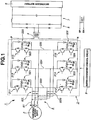
- FIG. 1 is used for illustrating the outline of a power conversion system to which an embodiment of the present invention is applied.
- a power conversion system 1 of this example is a system to convert three-phase ac power supplied from a three-phase ac power supply or power source 2, directly to single-phase ac power, with a power conversion apparatus or device 3 according to the embodiment of the present invention, to step up or down the single-phase ac power to an appropriate voltage with a transformer 4, and thereafter to convert the ac power to dc power with a rectifier 5, and thereby to charge a secondary battery 6.
- a smoothing circuit 7 There is further provided a smoothing circuit 7.
- a filter circuit 8 is provided, in power conversion system 1 of this example, for attenuating higher harmonics for noise suppression for each phase of output lines (R phase, S phase and T phase) to supply the three-phase ac power from three-phase ac power supply or source 2.
- Filter circuit 8 of this example includes three filter reactors 81 connected with the three phases R, S and T, respectively, and six filter condensers or capacitors 82L, 82R connected among the three phases R, S and T.
- a layout of filter condensers 82L, 82R (shown in FIGS. 3 ⁇ 6 , as filter condensers 821 ⁇ 836) is explained later.
- the three-phase ac power is supplied through filter circuit 8, to power conversion apparatus 3, and converted to the signal-phase ac power.
- Power conversion apparatus 3 of this example includes 6 bidirectional switching devices 31 arranged in a matrix corresponding to the R, S and T phases.
- a reference numeral 31 is used, as a generic term, to denote one of the bidirectional switching devices generally, and reference numerals 311 ⁇ 316 are used to denote a specific one of the six bidirectional switching devices, as shown in FIG. 1 .
- Each of the bidirectional switching devices 31 of this example is an IGBT module including a semiconductor switching element in the form of an IGBT (Insulated Gate Bipolar Transistor), and an anti-parallel freewheel diode or flyback diode combined in an anti-parallel connection.
- the construction of each bidirectional switching device 31 is not limited to the construction shown in the figure. For example, it is optional to employ a construction including two reverse blocking IGBT elements in the anti-parallel connection.
- a snubber circuit 32 is provided for each of bidirectional switching devices 31, to protect the corresponding bidirectional switching device 31 from surge voltage generated with ON/OFF operation of the bidirectional switching device 31.
- Snubber circuit 32 is connected with the input side and the output side of the corresponding bidirectional switching device 31 and formed by a combination of one snubber condenser or capacitor and three diodes.
- a reference numeral 32 is used, as a generic term, to denote one of the snubber circuits generally, and reference numerals 321 ⁇ 326 are used to denote a specific one of the six snubber circuits, as shown in FIG. 1 .
- a matrix converter control circuit 9 is provided, in the power conversion system 1 of this example, for ON/OFF control of each of bidirectional switching devices 31 of power conversion apparatus 3.
- Matrix converter control circuit 9 receives, as inputs, a value of a voltage supplied from three-phase ac power supply 2, a value of a dc current currently being outputted, and a value of a target current command, controls the gate signal of each of bidirectional switching devices 31 in accordance with these inputs, adjusts the single-phase ac power outputted to transformer 4, and thereby obtains the dc power corresponding to a target.
- Transformer 4 increases or decreases the voltage of single-phase ac power obtained by conversion of power conversion apparatus 3, to a predetermined value.
- Rectifier 5 includes four rectifying diodes and convers the single-phase ac power of the adjusted voltage into dc power.
- Smoothing circuit 7 includes a coil and a condenser or capacitor and smooths pulsation included in the dc current obtained by the rectification, into a condition closer to the dc current.
- the thus-constructed power conversion system 1 of this example converts the three-phase ac power supplied from three-phase power supply 2, directly into the single-phase ac power with power conversion apparatus 3, and convers the single-phase ac power into the dc power after the adjustment to a desired voltage.
- secondary battery 6 is charged.
- the power conversion system 1 is merely one example to which the power conversion apparatus 3 according to the present invention is applied.
- the present invention is not limited to this example in which the present invention is applied to the power conversion system 1.
- the present invention is applicable to other power conversion systems when at least one of the power before conversion and the power after conversion is polyphase ac power.
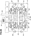
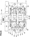
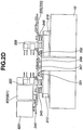
- FIGS. 2 ⁇ 6 are views for illustrating the spatial layout or arrangement of parts constituting power conversion apparatus 3 shown in FIG. 1 .
- the same reference numerals are used for identical parts shown in FIG. 1 to show the correspondence in the figures.
- FIG. 2 includes FIGS. 2A ⁇ 2D .
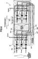
- FIG. 2A is a plan view showing an intermediate state during the assembly process, in which the six bidirectional switching devices 31 (also referred to as the IGBT modules) are mounted on an upper surface of a heat sink 10.
- FIG. 2B is a plan view showing an intermediate state during the assembly process, in which busbars are further mounted, for connecting terminals of the bidirectional switching devices 31.
- FIG. 2C is a plan view showing an intermediate state during the assembly process, in which, of the three diodes forming the snubber circuit 32, and the filter condensers 82 of filter circuit, the left side three filter condensers are mounted.
- FIG. 2D is a side view showing the intermediate state during the assembly process. Since constituent parts of power conversion apparatus 3 of this example are overlapped in the plan view, in the following explanation, main portions are shown in another drawing.
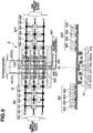
- each bidirectional switching device 31 of this example includes an input terminal, an output terminal and an intermediate or midpoint terminal between the two IGBTs arranged in a pair, and the inpute terminal, output terminal and intermediate terminal are provided on the upper side of the module package.
- the left side terminals of the three left side bidirectional switching devices 311, 313 and 315 are input terminals
- the right side terminals of the three left side bidirectional switching devices 311, 313 and 315 are output terminals
- the central terminals of the three left side bidirectional switching devices 311, 313 and 315 are intermediate terminals.
- the right side terminals of the three right side bidirectional switching devices 312, 314 and 316 are input terminals
- the left side terminals of the three right side bidirectional switching devices 312, 314 and 316 are output terminals
- the central terminals of the three right side bidirectional switching devices 312, 314 and 316 are intermediate terminals.
- Gate terminals of bidirectional switching devices 31 are provided in another part of the module package and omitted in the figure.
- the six bidirectional switching devices 311 ⁇ 316 are fixed on the upper surface of heat sink 10, by fastening means such as bolts. As shown in these figures, the six bidirectional switching devices 311 ⁇ 316 are arranged in three pairs: a first pair of bidirectional switching devices 311 and 312 disposed, respectively, on the left and right sides of a center line CL, a second pair of bidirectional switching devices 313 and 314 disposed, respectively, on the left and right sides of the center line CL, and a third pair of bidirectional switching devices 31 5 and 316 disposed, respectively, on the left and right sides of the center line CL.
- the bidirectional switching devices 311 and 312 are disposed side by side, on the left and right side of center line CL, respectively, along the extending direction in which the three terminals (input terminal, output terminal and intermediate terminals) of each bidirectional switching device 31 are extended or arranged; the bidirectional switching devices 313 and 314 are disposed side by side, on the left and right side of center line CL, respectively, along the extending direction; and the bidirectional switching devices 315 and 316 are disposed side by side, on the left and right side of center line CL, respectively, along the extending direction.
- this arrangement is also expressed as "juxtaposition, or parallel arrangement, with respect to center line CL or output lines P, N connecting the output terminals". This arrangement is different from the arrangement shown in FIG. 5 .
- the paired bidirectional switching devices are two bidirectional switching devices connected with the same one of the R, S, T phases of the input line.
- the right end terminals of left side bidirectional switching devices 311, 313 and 315 on the left side of center line CL are all output terminals, and the left end terminals of left side bidirectional switching devices 311, 313 and 315 are all input terminals.
- the left end terminals of right side bidirectional switching devices 312, 314 and 316 on the right side of center line CL are all output terminals, and the right end terminals of right side bidirectional switching devices 312, 314 and 316 are all input terminals.
- the input lines R, S and T of one branch branching off from the input lines of three-phase ac power supply 2 are connected in an inward direction toward the center line CL.
- the input lines R, S and T of the other branch branching off from the input lines of three-phase ac power supply 2 are connected in an inward direction toward the center line CL.
- the R phase is connected to the input terminals of bidirectional switching devices 311 and 312; the S phase is connected to the input terminals of bidirectional switching devices 313 and 314; and the T phase is connected to the input terminals of bidirectional switching devices 315 and 316.
- the input lines R, S and T on the left side are extended and connected in the inward direction toward center line CL, and the input lines R, S and T on the right side are also extended and connected in the inward direction toward center line CL.
- the input lines R, S and T extending from three-phase ac power supply 2 to power conversion apparatus 3 branch off at the position between the filter reactors 81 and the filter condensers 82L and 82R.
- the input lines R, S and T are divided into two branches on the upstream side of filter reactors 81, and the filter reactors 81 are provided for each of the branches of the input lines R, S and T.
- a busbar 331 forming an output line P of power conversion apparatus 3 is connected with the right end output terminals of bidirectional switching devices 311, 313 and 315 on the left side of center line CL.
- a busbar 332 forming an output line N of power conversion apparatus 3 is connected with the left end output terminals of bidirectional switching devices 312, 314 and 316 on the right side of center line CL.
- the forward ends of the busbars 331 and 332 are connected with transformer 4.
- Busbars including these busbars 331 and 332 and busbars mentioned herein below are made of conductor such as copper, superior in the electrical conductivity.
- a busbar 333 connects the input terminals of bidirectional switching devices 311 and 312 paired with each other and disposed on the left and right sides of center line CL.
- a busbar 334 connects the input terminals of bidirectional switching devices 313 and 314 paired with each other and disposed on the left and right sides of center line CL.
- a busbar 335 connects the input terminals of bidirectional switching devices 315 and 316 paired with each other and disposed on the left and right sides of center line CL.
- the wirings corresponding to the busbars are shown with the same reference numerals, respectively.
- busbars 333 ⁇ 335 are arranged to intersect the busbars 331 and 332 forming the output lines P and N as viewed in a plan view. However, as shown in the side view of FIG. 3 , the busbars 333 ⁇ 335 connecting the input terminals are formed at a position higher than the busbars 331 and 332, and thereby arranged to avoid interference therebetween with a multilevel crossing structure of overpass or underpass.
- the filter condensers 82L and 82R provided between two of the phases can be used in common by employing the arrangement in which the bidirectional switching devices 311 and 322 disposed on the left and right sides of center line in the first pair are connected, the bidirectional switching devices 313 and 324 in the second pair are connected, and the bidirectional switching devices 315 and 326 in the third pair are connected.
- filter condenser 821 is provided between the R and S phases on the left side in FIG. 3
- filter condenser 824 is provided between the R and S phases on the right side in FIG. 3 .
- the busbar 333 connects the input terminals of bidirectional switching devices 311 and 312 to which the R phase is inputted.
- noises in the R phase of three-phase ac power supply 2 are removed by cooperative filtering operation of the two filter condensers 821 and 824. Consequently, it is possible to reduce the capacity of one filter condenser and hence to reduce the sizes of the filter condensers. The same is applied to the S phase and the T phase.
- the filter circuit in this example includes the six filter condensers 821 ⁇ 826 so arranged that three of the six filter condensers are connected among the input lines on the left side of center line CL and the remaining three are connected among the input lines on the right side of center line CL, as shown in FIG. 3 .
- the left side filter condenser 821 is provided between the S phase and the R phase which corresponds to the input terminal of bidirectional switching device 311.
- the left side filter condenser 822 is provided between the T phase and the S phase which corresponds to the input terminal of bidirectional switching device 313.
- the left side filter condenser 823 is provided between the R phase and the T phase which corresponds to the input terminal of bidirectional switching device 31 5.
- the right side filter condenser 824 is provided between the S phase and the R phase corresponding to the input terminal of bidirectional switching device 313.
- the right side filter condenser 825 is provided between the T phase and the S phase corresponding to the input terminal of bidirectional switching device 314.
- the right side filter condenser 826 is provided between the R phase and the T phase corresponding to the input terminal of bidirectional switching device 316.
- the left three and the right three of filter condensers 821 ⁇ 826 are disposed on the outer sides of the region in which the six bidirectional switching devices 311 ⁇ 316 are formed, with respect to center line CL.
- the left three and the right three of filter condensers 821 ⁇ 826 are fixed on upper part of the busbars.
- the left three and the right three of filer condensers 821 ⁇ 826 are mounted on the left and right sides of center line CL as shown in FIG. 2 showing the plan view and side view of an actual apparatus.
- busbar 331 forms the output line P connecting the output terminals of bidirectional switching devices 311, 313 and 315 and leading to transformer 4.
- Busbar 332 forms the output line N connecting the output terminals of bidirectional switching devices 312, 314 and 316 and leading to transformer 4.
- Busbar 333 is a busbar connecting the input terminals of bidirectional switching devices 311 and 312, and including a first end portion which extends outwards in a leftward direction beyond the input terminal of bidirectional switching device 311 and which is connected with a busbar 336 to connect the filter condenser 823, and a second end portion which extends outwards in a rightward direction beyond the input terminal of bidirectional switching device 312 and which is connected with a busbar 337 to connect the filter condenser 826 (cf. FIG. 2C and FIG. 3 for the connection state of filter condensers 823 and 826).
- Busbars 336 and 337 connected with both ends of busbar 333 are inclined with respect to a line connecting the input terminals of bidirectional switching devices 311, 313 and 315, that is a line extending in an up and down direction as viewed in FIG. 2C .
- Busbar 334 is a busbar connecting the input terminals of bidirectional switching devices 313 and 314, and including a first end portion which extends outwards in the leftward direction beyond the input terminal of bidirectional switching device 313 and which is connected with a busbar 338 to connect the filter condensers 821 and 822, and a second end portion which extends outwards in the rightward direction beyond the input terminal of bidirectional switching device 314 and which is connected with a busbar 339 to connect the filter condensers 824 and 825 (cf. FIG. 2C and FIG. 3 for the connection state of filter condensers 821, 822, 824 and 825).
- Busbars 338 and 339 connected with both ends of busbar 334 extend along the line connecting the input terminals of bidirectional switching devices 311, 313 and 315, that is the line extending in the up and down direction as viewed in a left upper view( FIG. 2C ?) of FIG. 2 .
- Busbar 335 is a busbar connecting the input terminals of bidirectional switching devices 315 and 316, and including a first end portion which extends outwards in the leftward direction beyond the input terminal of bidirectional switching device 31 5 and which is connected with a busbar 340 to connect the filter condenser 823, and a second end portion which extends outwards in the rightward direction beyond the input terminal of bidirectional switching device 316 and which is connected with a busbar 341 to connect the filter condenser 826 (cf. FIG. 2C and FIG. 3 for the connection state of filter condensers 823 and 826).
- Busbars 340 and 341 connected with both ends of busbar 335 are inclined with respect to the line connecting the input terminals of bidirectional switching devices 311, 313 and 315, that is the line extending in the up and down direction as viewed in FIG. 2C .
- these busbars 333, 334 and 335 are connected with the input terminals of bidirectional switching devices 311 ⁇ 316 through a plurality of busbars 345 and 346, and disposed at a position or level above the busbars 331 and 332 forming the output lines P and N.
- the busbars 333 ⁇ 335 and the busbars 331 and 332 are separated in the height or vertical direction with a predetermined clearance without interference in the manner of grade separation or multilevel crossing.
- filter condensers 821, 822 and 823 are disposed on the outer side with respect to center line CL, and arranged so that the centers of filter condensers 821, 822 and 823 are located, respectively, at the apexes of a triangle (preferably an isosceles triangle or an equilateral or regular triangle) which is oriented so that one of the apexes is directed in the outward direction.
- a triangle preferably an isosceles triangle or an equilateral or regular triangle
- Filter condenser 821 connected between the R phase and S phase is mounted on the upper surface of a busbar 342.
- Filter condenser 822 connected between the S phase and T phase is mounted on the upper surface of a busbar 343.
- These two busbars 342 and 343 are inclined with respect to a line connecting the input terminals of bidirectional switching devices 311, 313 and 315, that is, a line extending in the up and down direction in FIG. 2C .
- these two busbars 342 and 343 are extended across the line connecting the input terminals of bidirectional switching devices 311, 313 and 315, that is, the line extending in the up and down direction in FIG. 2C , and connected with busbars 333, 342 and 335.
- Filter condensers 824 and 825 on the right side of center line CL are arranged symmetrically with respect to center line CL.
- busbars 342 and 343 are inclined with respect to the line connecting the input terminals of bidirectional switching devices 311, 313 and 31 5, it is possible to make the wiring distance equal to the wiring distance of the filter condenser 823 connected between the R phase and T phase, as much as possible. Therefore, it is possible to attain tuning among filter condensers 821, 822 and 823.
- busbars 342 and 343 are provided across the line connecting the input terminals of bidirectional switching devices 311, 313 and 315, it is possible to reduce the connection distances of filter condensers 821 and 822 with busbars 333, 334 and 335, and hence it is possible to reduce the size of power conversion apparatus 3.
- each of the filter condensers 821 ⁇ 826 is disposed on the upper surface of the busbars, namely the arrangement in which the bidirectional switching devices 311 ⁇ 316 are disposed on one side of the busbars, and the filter condensers 821 ⁇ 826 are on the opposite side of the busbars, the design freedom or flexibility of layout of filter condensers 821 ⁇ 826 is increased.
- Filter condenser 823 connected between the R phase and T phase is mounted on the upper surface of a busbar 344 connected between busbars 336 and 340.
- This busbar 344 is disposed so that busbar 344 is parallel to the line connecting the input terminals of bidirectional switching devices 311, 313 and 315.
- snubber circuit 321 of bidirectional switching device 311 for example, as shown in FIG. 1 , a first terminal of snubber circuit 321 is connected with the input terminal of bidirectional switching device 311, a second terminal of snubber circuit 321 is connected with the intermediate terminal of bidirectional switching device 311, and a third terminal is connected with the output terminal of bidirectional switching device 311. Therefore, as shown in FIGS. 2C and 2D , the three diodes are fixed and connected, respectively, with brackets 351 ⁇ 356 which are made of conductor and connected with the intermediate terminals of bidirectional switching devices 31 L and 31 R. FIG. 2D shows only the bracket 355.
- the conversion system uses a relatively large sized electrolytic condenser for the snubber condensers, and employs a snubber condenser 327 common to the six snubber circuits 321 ⁇ 326 (cf. FIG. 3 ).
- Busbars 347 and 348 for connecting this snubber condenser 327 and the three diodes are formed to extend, between the busbars 331 and 332 forming the output lines P and N, in the same direction as the output lines.
- the two busbars 347 and 348 connected with snubber condenser 327 are fixed at a level higher than the busbars 331 and 332 forming the output lines P and N, and lower than the busbars 333, 334 and 335.
- These two busbars 347 and 348 are supported by heat sink 10 or a base (not shown) other than heat sink 10. It is optional to provide insulating coating on the surfaces of busbars 347 and 348 to prevent short-circuit with busbars 333, 334 and 335.
- busbar 311 and 312 As to the layout of busbar 311 and 312 forming output lines P and N and busbars 347 and 348 leading to snubber condenser 327, the disposition of busbars 347 and 348 between busbars 311 and 312 makes it possible to reduces the wiring distances of output lines P and N and the wiring distances to snubber condenser 327. Moreover, the setting of busbars 347 and 348 at the position higher than busbar 311 and 312 makes it possible to reduce the distances from the diodes of snubber circuits 321 ⁇ 326.
- the left side three filter condensers 82L and the right side three filter condensers 82R are disposed, respectively, on the outer sides of bidirectional switching devices 311, 313 and 315, and on the outer side of bidirectional switching devices 312, 314 and 316 with respect to center line CL as the center.
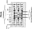
- FIGS. 4A and 4B it is possible to place the left side three filter condensers 82L and the right side three filter condensers 82R, between the bidirectional switching devices 311, 313 and 315 on the left side of center line CL and the bidirectional switching devices 312, 314 and 316 on the right side of center line CL.
- the bidirectional switching devices 311, 313 and 315 are disposed on the right side of center line CL, and the bidirectional switching devices 312, 314 and 316 are disposed on the right side of center line CL.
- the bidirectional switching devices 311, 313 and 315 and the bidirectional switching devices 312, 314 and 316 are disposed along the center line CL.
- the three bidirectional switching devices 311, 313 and 315 are disposed on the left side of center line CL
- the three bidirectional switching devices 312, 314 and 316 are disposed on the right side of center line
- the input terminals and the output terminals of these six bidirectional switching devices 311 ⁇ 316 are arranged symmetrically with respect to center line CL in a manner of line symmetry or reflection symmetry.
- FIG. 3 shows that as shown in FIG.
- the three bidirectional switching devices 311, 313 and 315 are disposed on the left side of center line CL
- the three bidirectional switching devices 312, 314 and 316 are disposed on the right side of center line
- the input and output terminals of the left side three bidirectional switching devices 311, 313 and 315 and the input and output terminals of the right side bidirectional switching devices 312m 314 and 316 are arranged in the same manner.
- the two set of the input lines R, S and T are extended in the same direction (in the rightward direction in the illustrated example) and connected with the input terminals of the respective bidirectional switching devices.
- filter condensers 821 ⁇ 826 are provided between two phases so that each of the six bidirectional switching devices 311 ⁇ 316 corresponds uniquely to one of the six filter condensers.
- FIG. 7 it is possible to employ an arrangement in which filter condensers 821 ⁇ 826 are provided between two phases so that each of the six bidirectional switching devices 311 ⁇ 316 corresponds uniquely to a plurality of filter condensers (two of filter condensers in the illustrated example).
- the filter condensers may be disposed in a center region of the power conversion apparatus 3 as shown in FIG. 8 , or may be disposed on the outer sides of power conversion apparatus 3, as shown in FIG. 9 .
- the filter condensers are disposed in the center region of the power conversion apparatus 3 as shown in FIG. 8 , it is possible to utilize free space and hence to restrain or reduce the size of power conversion apparatus 3 as much as possible.
- the bidirectional switching devices 311, 313 and 315 correspond to a first switching device or element in the claims of the present invention
- the bidirectional switching devices 312, 314 and 316 correspond to a second switching device or element in the claims of the present invention.
- the power conversion apparatus 3 corresponds to a conversion circuit in the claims of the present invention.
- the filter condensers 821 ⁇ 826, 831 ⁇ 836 correspond to condensers in the claims of the present invention.
- the busbars 331 and 332 corresponds to an output line in the claims of the present invention.
Description
- The present invention relates to a power conversion device or apparatus for converting ac power of utility frequency or commercial power frequency, directly into desired ac power.
- There is known a matrix converter as a power conversion apparatus for converting ac power to ac power directly and efficiently with a construction requiring a smaller number of component parts and enabling size reduction of the apparatus (Patent Document 1).
- However, an output line is long in the above-mentioned matrix converter of earlier technology in which a plurality of IGBTs (Insulated Gate Bipolar Transistors) are disposed in an inline arrangement, and the output line is connected collectively from each IGBT. Especially, in a power conversion apparatus in which high frequency ac current flows through the output line, the apparatus becomes susceptible to the influence of L component if the length of a wiring is great.
- Patent Document 1:
JP2006-333590 A -
JP2001045772A - It is an object of the present invention to provide power conversion device or apparatus for reducing a length of an output line.
- This is achieved by a power conversion apparatus according to
claim 1. According to the present invention, a plurality of switching devices forming a power conversion circuit are arranged so that an
output line is located below an input line in an up and down direction. - According to the present invention, the switching devices are arranged and the output line is placed below the input line, so that it is possible to reduce the length of the output line.
-
-
FIG. 1 is an electric circuit diagram showing a power conversion system to which one embodiment of the present invention is applied. -
FIG. 2A is a plan view showing a power conversion apparatus according to the embodiment of the present invention, in an intermediate state under an assembly process. -
FIG. 2B is a plan view showing the power conversion apparatus according to the embodiment of the present invention, in an intermediate state under the assembly process. -
FIG. 2C is a plan view showing the power conversion apparatus according to the embodiment of the present invention, in an intermediate state under the assembly process. -
FIG. 2D is a side view showing the power conversion apparatus according to the embodiment of the present invention, in an intermediate state under the assembly process. -
FIG. 3 is a view showing a layout of IGBTs and filter condensers of the power conversion apparatus shown inFIG. 2 , in a plan view and a side view. -
FIG. 4A is a plan view showing another layout of the IGBTs and filter condensers shown inFIG. 3 . -
FIG. 4B is a side view ofFIG. 4A . -
FIG. 5 is a view showing still another layout of the IGBTs and filter condensers shown inFIG. 3 , in a plan view. -
FIG. 6 is a view showing still another layout of the IGBTs and filter condensers shown inFIG. 3 , in a plan view. -
FIG. 7 is an electric circuit diagram showing a power conversion system to which another embodiment of the present invention is applied. -
FIG. 8 is a view showing a layout of the IGBTs and filter condensers shown inFIG. 7 , in a plan view and a side view. -
FIG. 9 is a view showing another layout of the IGBTs and filter condensers shown inFIG. 7, in a plan view and a side view. - First,
FIG. 1 is used for illustrating the outline of a power conversion system to which an embodiment of the present invention is applied. Apower conversion system 1 of this example is a system to convert three-phase ac power supplied from a three-phase ac power supply orpower source 2, directly to single-phase ac power, with a power conversion apparatus ordevice 3 according to the embodiment of the present invention, to step up or down the single-phase ac power to an appropriate voltage with atransformer 4, and thereafter to convert the ac power to dc power with a rectifier 5, and thereby to charge asecondary battery 6. There is further provided asmoothing circuit 7. - A
filter circuit 8 is provided, inpower conversion system 1 of this example, for attenuating higher harmonics for noise suppression for each phase of output lines (R phase, S phase and T phase) to supply the three-phase ac power from three-phase ac power supply orsource 2.Filter circuit 8 of this example includes threefilter reactors 81 connected with the three phases R, S and T, respectively, and six filter condensers orcapacitors filter condensers FIGS. 3∼6 , asfilter condensers 821∼836) is explained later. - In the power conversion system of this example, the three-phase ac power is supplied through
filter circuit 8, topower conversion apparatus 3, and converted to the signal-phase ac power.Power conversion apparatus 3 of this example includes 6 bidirectional switching devices 31 arranged in a matrix corresponding to the R, S and T phases. Hereinafter, a reference numeral 31 is used, as a generic term, to denote one of the bidirectional switching devices generally, andreference numerals 311∼316 are used to denote a specific one of the six bidirectional switching devices, as shown inFIG. 1 . - Each of the bidirectional switching devices 31 of this example is an IGBT module including a semiconductor switching element in the form of an IGBT (Insulated Gate Bipolar Transistor), and an anti-parallel freewheel diode or flyback diode combined in an anti-parallel connection. The construction of each bidirectional switching device 31 is not limited to the construction shown in the figure. For example, it is optional to employ a construction including two reverse blocking IGBT elements in the anti-parallel connection.
- A snubber circuit 32 is provided for each of bidirectional switching devices 31, to protect the corresponding bidirectional switching device 31 from surge voltage generated with ON/OFF operation of the bidirectional switching device 31. Snubber circuit 32 is connected with the input side and the output side of the corresponding bidirectional switching device 31 and formed by a combination of one snubber condenser or capacitor and three diodes. Hereinafter, a reference numeral 32 is used, as a generic term, to denote one of the snubber circuits generally, and
reference numerals 321∼326 are used to denote a specific one of the six snubber circuits, as shown inFIG. 1 . - A matrix
converter control circuit 9 is provided, in thepower conversion system 1 of this example, for ON/OFF control of each of bidirectional switching devices 31 ofpower conversion apparatus 3. Matrixconverter control circuit 9 receives, as inputs, a value of a voltage supplied from three-phase acpower supply 2, a value of a dc current currently being outputted, and a value of a target current command, controls the gate signal of each of bidirectional switching devices 31 in accordance with these inputs, adjusts the single-phase ac power outputted to transformer 4, and thereby obtains the dc power corresponding to a target. -
Transformer 4 increases or decreases the voltage of single-phase ac power obtained by conversion ofpower conversion apparatus 3, to a predetermined value. Rectifier 5 includes four rectifying diodes and convers the single-phase ac power of the adjusted voltage into dc power.Smoothing circuit 7 includes a coil and a condenser or capacitor and smooths pulsation included in the dc current obtained by the rectification, into a condition closer to the dc current. - The thus-constructed
power conversion system 1 of this example converts the three-phase ac power supplied from three-phase power supply 2, directly into the single-phase ac power withpower conversion apparatus 3, and convers the single-phase ac power into the dc power after the adjustment to a desired voltage. Thus,secondary battery 6 is charged. Thepower conversion system 1 is merely one example to which thepower conversion apparatus 3 according to the present invention is applied. The present invention is not limited to this example in which the present invention is applied to thepower conversion system 1. The present invention is applicable to other power conversion systems when at least one of the power before conversion and the power after conversion is polyphase ac power. -
FIGS. 2∼6 are views for illustrating the spatial layout or arrangement of parts constitutingpower conversion apparatus 3 shown inFIG. 1 . In these figures, the same reference numerals are used for identical parts shown inFIG. 1 to show the correspondence in the figures. -
FIG. 2 includesFIGS. 2A∼2D .FIG. 2A is a plan view showing an intermediate state during the assembly process, in which the six bidirectional switching devices 31 (also referred to as the IGBT modules) are mounted on an upper surface of aheat sink 10.FIG. 2B is a plan view showing an intermediate state during the assembly process, in which busbars are further mounted, for connecting terminals of the bidirectional switching devices 31.FIG. 2C is a plan view showing an intermediate state during the assembly process, in which, of the three diodes forming the snubber circuit 32, and the filter condensers 82 of filter circuit, the left side three filter condensers are mounted.FIG. 2D is a side view showing the intermediate state during the assembly process. Since constituent parts ofpower conversion apparatus 3 of this example are overlapped in the plan view, in the following explanation, main portions are shown in another drawing. - As shown in
FIG. 2 andFIG. 3 , each bidirectional switching device 31 of this example includes an input terminal, an output terminal and an intermediate or midpoint terminal between the two IGBTs arranged in a pair, and the inpute terminal, output terminal and intermediate terminal are provided on the upper side of the module package. Among the sixbidirectional switching devices 311∼316 shown inFIG. 3 , the left side terminals of the three left sidebidirectional switching devices bidirectional switching devices bidirectional switching devices bidirectional switching devices 311∼316 shown inFIG. 3 , the right side terminals of the three right sidebidirectional switching devices bidirectional switching devices bidirectional switching devices - As shown in
FIG. 2 andFIG. 3 , the sixbidirectional switching devices 311∼316 are fixed on the upper surface ofheat sink 10, by fastening means such as bolts. As shown in these figures, the sixbidirectional switching devices 311∼316 are arranged in three pairs: a first pair ofbidirectional switching devices bidirectional switching devices bidirectional switching devices bidirectional switching devices bidirectional switching devices FIG. 5 . The paired bidirectional switching devices are two bidirectional switching devices connected with the same one of the R, S, T phases of the input line. - With this arrangement or juxtaposition including the
bidirectional switching devices busbars 331 and 332) in one direction at a minimum distance. Since influence of L component is increased by an increase of wiring outputting high frequency ac power, the arrangement of this example can restrain the influence of the L component. This effect of the arrangement of this example is more advantageous as compared to the example shown inFIG. 5 . Thus, the output lines P and N are almost straight up totransformer 4. - As mentioned before, the right end terminals of left side
bidirectional switching devices bidirectional switching devices bidirectional switching devices bidirectional switching devices - To the input terminals at the left ends of
bidirectional switching devices ac power supply 2 are connected in an inward direction toward the center line CL. To the input terminals at the right end ofbidirectional switching devices ac power supply 2 are connected in an inward direction toward the center line CL. The R phase is connected to the input terminals ofbidirectional switching devices bidirectional switching devices bidirectional switching devices heat sink 10 as compared to the arrangement in the other example shown inFIG. 6 . - In the configuration of
FIG. 1 , the input lines R, S and T extending from three-phaseac power supply 2 topower conversion apparatus 3 branch off at the position between thefilter reactors 81 and thefilter condensers filter reactors 81, and thefilter reactors 81 are provided for each of the branches of the input lines R, S and T. - A
busbar 331 forming an output line P ofpower conversion apparatus 3 is connected with the right end output terminals ofbidirectional switching devices busbar 332 forming an output line N ofpower conversion apparatus 3 is connected with the left end output terminals ofbidirectional switching devices busbars transformer 4. Busbars including thesebusbars - A
busbar 333 connects the input terminals ofbidirectional switching devices busbar 334 connects the input terminals ofbidirectional switching devices busbar 335 connects the input terminals ofbidirectional switching devices FIG. 1 , the wirings corresponding to the busbars are shown with the same reference numerals, respectively. Thesebusbars 333∼335 are not essential for the function ofpower conversion apparatus 3, and therefore, it is optional to omit these busbars. - These
busbars 333∼335 are arranged to intersect thebusbars FIG. 3 , thebusbars 333∼335 connecting the input terminals are formed at a position higher than thebusbars - The
filter condensers bidirectional switching devices bidirectional switching devices bidirectional switching devices filter condenser 821 is provided between the R and S phases on the left side inFIG. 3 , andfilter condenser 824 is provided between the R and S phases on the right side inFIG. 3 . Thebusbar 333 connects the input terminals ofbidirectional switching devices ac power supply 2 are removed by cooperative filtering operation of the twofilter condensers - The filter circuit in this example includes the six
filter condensers 821∼826 so arranged that three of the six filter condensers are connected among the input lines on the left side of center line CL and the remaining three are connected among the input lines on the right side of center line CL, as shown inFIG. 3 . The leftside filter condenser 821 is provided between the S phase and the R phase which corresponds to the input terminal ofbidirectional switching device 311. Similarly, the leftside filter condenser 822 is provided between the T phase and the S phase which corresponds to the input terminal ofbidirectional switching device 313. The leftside filter condenser 823 is provided between the R phase and the T phase which corresponds to the input terminal of bidirectional switching device 31 5. Similarly, the rightside filter condenser 824 is provided between the S phase and the R phase corresponding to the input terminal ofbidirectional switching device 313. The rightside filter condenser 825 is provided between the T phase and the S phase corresponding to the input terminal ofbidirectional switching device 314. The rightside filter condenser 826 is provided between the R phase and the T phase corresponding to the input terminal ofbidirectional switching device 316. - With the arrangement in which the six
filter condensers 821∼826 are arranged so that three are on the left side of center line CL and the other three filter condensers are on the right side, for the sixbidirectional switching devices 311∼316 arranged so that three are on the left side of center line CL and the other three switching devices are on the right side, it is possible to reduce the distance or length of connection wire routing for each offilter condensers 821∼826 andbidirectional switching devices 311∼316. - In this example, the left three and the right three of
filter condensers 821∼826 are disposed on the outer sides of the region in which the sixbidirectional switching devices 311∼316 are formed, with respect to center line CL. Concretely, as shown inFIG. 2D , the left three and the right three offilter condensers 821∼826 are fixed on upper part of the busbars. With the arrangement in which filtercondensers 821∼826 are so arranged that thebidirectional switching devices 311∼316 are located between the left three filter condensers and the right three filter condensers, it is possible to minimize the spacing between the left and right bidirectional switching devices 31 L and 31 R in the left and right direction. Therefore, it is possible to set the distance or length in the left and right direction, ofheat sink 10 at a minimum value. As a result, it is possible to reduce the size ofheat sink 10 as compared to the arrangement in another example shown inFIG. 4A . - The left three and the right three of
filer condensers 821∼826 are mounted on the left and right sides of center line CL as shown inFIG. 2 showing the plan view and side view of an actual apparatus. - Beforehand, the explanation is directed to the connection structure of the busbars. As shown in
FIG. 2B ,busbar 331 forms the output line P connecting the output terminals ofbidirectional switching devices transformer 4.Busbar 332 forms the output line N connecting the output terminals ofbidirectional switching devices transformer 4.Busbar 333 is a busbar connecting the input terminals ofbidirectional switching devices bidirectional switching device 311 and which is connected with abusbar 336 to connect thefilter condenser 823, and a second end portion which extends outwards in a rightward direction beyond the input terminal ofbidirectional switching device 312 and which is connected with abusbar 337 to connect the filter condenser 826 (cf.FIG. 2C andFIG. 3 for the connection state offilter condensers 823 and 826).Busbars busbar 333 are inclined with respect to a line connecting the input terminals ofbidirectional switching devices FIG. 2C . -
Busbar 334 is a busbar connecting the input terminals ofbidirectional switching devices bidirectional switching device 313 and which is connected with abusbar 338 to connect thefilter condensers bidirectional switching device 314 and which is connected with abusbar 339 to connect thefilter condensers 824 and 825 (cf.FIG. 2C andFIG. 3 for the connection state offilter condensers Busbars busbar 334 extend along the line connecting the input terminals ofbidirectional switching devices FIG. 2C ?) ofFIG. 2 . -
Busbar 335 is a busbar connecting the input terminals ofbidirectional switching devices busbar 340 to connect thefilter condenser 823, and a second end portion which extends outwards in the rightward direction beyond the input terminal ofbidirectional switching device 316 and which is connected with abusbar 341 to connect the filter condenser 826 (cf.FIG. 2C andFIG. 3 for the connection state offilter condensers 823 and 826).Busbars busbar 335 are inclined with respect to the line connecting the input terminals ofbidirectional switching devices FIG. 2C . - As shown in
FIG. 2D , thesebusbars bidirectional switching devices 311∼316 through a plurality ofbusbars busbars busbars 333∼335 and thebusbars - As shown by broken lines in
FIG. 2C ,filter condensers filter condensers filter condensers power conversion apparatus 3, and to attain tuning among the condensers properly. Furthermore, with the arrangement in which the triangle is so oriented that one of the apexes of the triangle is directed in the outward direction, it is possible to improve the balance of wiring connecting to the condensers and to decrease the distance to each of thebusbars -
Filter condenser 821 connected between the R phase and S phase is mounted on the upper surface of abusbar 342.Filter condenser 822 connected between the S phase and T phase is mounted on the upper surface of abusbar 343. These twobusbars bidirectional switching devices FIG. 2C . Moreover, these twobusbars bidirectional switching devices FIG. 2C , and connected withbusbars Filter condensers - With the arrangement in which
busbars bidirectional switching devices filter condenser 823 connected between the R phase and T phase, as much as possible. Therefore, it is possible to attain tuning amongfilter condensers busbars bidirectional switching devices filter condensers busbars power conversion apparatus 3. With the arrangement in which each of thefilter condensers 821∼826 is disposed on the upper surface of the busbars, namely the arrangement in which thebidirectional switching devices 311∼316 are disposed on one side of the busbars, and thefilter condensers 821∼826 are on the opposite side of the busbars, the design freedom or flexibility of layout offilter condensers 821∼826 is increased. -
Filter condenser 823 connected between the R phase and T phase is mounted on the upper surface of abusbar 344 connected betweenbusbars busbar 344 is disposed so thatbusbar 344 is parallel to the line connecting the input terminals ofbidirectional switching devices - Following is explanation on an implementing example of three diodes and one snubber condenser or capacitor forming one of the snubber circuits 32 shown in
FIG. 1 . In the case of thesnubber circuit 321 ofbidirectional switching device 311, for example, as shown inFIG. 1 , a first terminal ofsnubber circuit 321 is connected with the input terminal ofbidirectional switching device 311, a second terminal ofsnubber circuit 321 is connected with the intermediate terminal ofbidirectional switching device 311, and a third terminal is connected with the output terminal ofbidirectional switching device 311. Therefore, as shown inFIGS. 2C and2D , the three diodes are fixed and connected, respectively, withbrackets 351∼356 which are made of conductor and connected with the intermediate terminals of bidirectional switching devices 31 L and 31 R.FIG. 2D shows only thebracket 355. - In this example, the conversion system uses a relatively large sized electrolytic condenser for the snubber condensers, and employs a
snubber condenser 327 common to the sixsnubber circuits 321∼326 (cf.FIG. 3 ).Busbars snubber condenser 327 and the three diodes are formed to extend, between thebusbars - As shown in
FIG. 2D andFIG. 3 , the twobusbars snubber condenser 327 are fixed at a level higher than thebusbars busbars busbars heat sink 10 or a base (not shown) other thanheat sink 10. It is optional to provide insulating coating on the surfaces ofbusbars busbars - As to the layout of
busbar busbars snubber condenser 327, the disposition ofbusbars busbars snubber condenser 327. Moreover, the setting ofbusbars busbar snubber circuits 321∼326. - According to this embodiment, it is possible to provide following advantages.
- 1) To the six
bidirectional switching devices 311∼316, three devices being on one of the left and right sides of center line CL, and the other three devices being on the other side, the sixfilter condensers 821∼826 are disposed so that three of the six filter condensers are disposed on the left side of center line CL to the three devices on the left side, and the remaining three filter condensers are disposed on the right side of center line CL to the right three bidirectional switching devices. Therefore, it is possible to reduce the routing or wiring distances offilter condensers 821∼826 andbidirectional switching devices 311∼316. - 2) In this example, the pair of
bidirectional switching devices bidirectional switching devices busbars busbars busbars 331 and 332) in one direction shortly without interference. Therefore, the layout of this example can restrain the influence of the L component or inductance though a longer wire for outputting high frequency ac power would be susceptible to the influence of the L component. - 3) In this example, the three of
filter condensers 821∼826 on the left side and the other three filter condensers on the right side are disposed on the outer sides of the region in which the sixbidirectional switching devices 311∼316 are provided, with respect to center line CL so that the region of the bidirectional switching devices is located between the three filter condensers on the left side and the other three filter condensers on the right side. Therefore, it is possible to minimize the spacing, in the left and right direction, between the left side bidirectional switching devices 31 L and the right side bidirectional switching devices 31 R. Consequently, it is possible to set the distance or dimension ofheat sink 10 in the left and right direction at a minimum distance, and hence to reduce the size ofheat sink 10. - 4) In this example,
busbars bidirectional switching devices bidirectional switching devices filter condensers - 5) In this example, to the input terminals of bidirectional switching devices 31 L, the left side input lines R, S and T are extended in the inward direction toward center line CL. Similarly, to the input terminals of bidirectional switching devices 31R, the right side input lines R, S and T are extended in the inward direction toward center line CL. Therefore, it is possible to reduce the distance or dimension of
heat sink 10 in the left and right direction. - 6) In this example,
filter condensers 821∼826 are disposed on the upper side of the busbars. In other words, thebidirectional switching devices 311∼316 are disposed on one side of the busbars, and thefilter condensers 821∼826 are disposed on the other side of the busbars. Therefore, the freedom of layout design offilter condensers 821∼826 is increased. - 7) In this example, as to the arrangement of
busbars busbars snubber condenser 327, thebusbars busbars snubber condensers 327. - 8) In this example, the
busbars busbars snubber circuits 321∼326. - 9) In this example, the three
filter condensers power conversion apparatus 3, and to achieve tuning among the condensers. - 10) In this example, the three condensers positioned so as to form a triangle are arranged so that one apex of the triangle is directed in the outward direction. Therefore, it is possible to improve the balance of wiring connected with the condensers as compared to the arrangement in which one apex is directed in the inward direction, and to reduce the distance to each of
busbars - 11) In this example, the
busbars bidirectional switching devices filter condenser 823 connected between the R phase and T phase, as much as possible. Therefore, it is possible to attain tuning amongfilter condensers - 12) In this example, the
busbars bidirectional switching devices filter condensers busbars power conversion apparatus 3. - According to the present invention, variations and modifications are possible, besides the preceding embodiment. Following is explanation on variation examples according to the present invention. However, there is no intention of limiting the present invention to the above-mentioned embodiment, and following embodiments. Members used in the above-mentioned embodiment are given the same reference numerals and explanation is omitted appropriately.
- In the above-mentioned embodiment, as shown in
FIG.3 , the left side threefilter condensers 82L and the right side threefilter condensers 82R are disposed, respectively, on the outer sides ofbidirectional switching devices bidirectional switching devices FIGS. 4A and4B , it is possible to place the left side threefilter condensers 82L and the right side threefilter condensers 82R, between thebidirectional switching devices bidirectional switching devices - Moreover, in the above-mentioned embodiment, as shown in
FIG. 3 , thebidirectional switching devices bidirectional switching devices FIG 5 , thebidirectional switching devices bidirectional switching devices - In the above-mentioned embodiment, as shown in
FIG.3 , the threebidirectional switching devices bidirectional switching devices bidirectional switching devices 311∼316 are arranged symmetrically with respect to center line CL in a manner of line symmetry or reflection symmetry. However, as shown inFIG. 6 , it is possible to employ an arrangement in which the threebidirectional switching devices bidirectional switching devices bidirectional switching devices switching devices 312m - Moreover, in the above-mentioned embodiment, as shown in
FIG. 3 ,filter condensers 821∼826 are provided between two phases so that each of the sixbidirectional switching devices 311∼316 corresponds uniquely to one of the six filter condensers. However, as shown inFIG. 7 , it is possible to employ an arrangement in which filtercondensers 821∼826 are provided between two phases so that each of the sixbidirectional switching devices 311∼316 corresponds uniquely to a plurality of filter condensers (two of filter condensers in the illustrated example). - In this case, the filter condensers may be disposed in a center region of the
power conversion apparatus 3 as shown inFIG. 8 , or may be disposed on the outer sides ofpower conversion apparatus 3, as shown inFIG. 9 . In the case of the arrangement in which the filter condensers are disposed in the center region of thepower conversion apparatus 3 as shown inFIG. 8 , it is possible to utilize free space and hence to restrain or reduce the size ofpower conversion apparatus 3 as much as possible. - The
bidirectional switching devices bidirectional switching devices power conversion apparatus 3 corresponds to a conversion circuit in the claims of the present invention. Thefilter condensers 821∼826, 831∼836 correspond to condensers in the claims of the present invention. Thebusbars
Claims (7)
- A power conversion apparatus for converting polyphase ac power directly to ac power, the power conversion apparatus comprising:a conversion circuit (3) including a plurality of first switching devices (311, 313, 315) connected, respectively, with phases (R, S, T) of the polyphase ac power, and configured to enable electrical switching operation in both directions, and a plurality of second switching devices (312, 314, 316) connected, respectively, with the phases (R, S, T) of the polyphase ac power, and configured to enable electrical switching operation in both directions;a plurality of input lines (R, S, T) connected, respectively, with input terminals of the first switching devices and input terminals of the second switching devices, anda first output line (331, P) connected with output terminals of the first switching devices, and a second output line (332, N) connected with output terminals of the second switching devices,as a spatial arrangement, output terminals of the first switching devices (311, 313, 315) being arranged in a row and output terminals of the second switching devices (312, 314, 316) being arranged in a row,characterized in thatthe first switching devices (311, 313, 315) and the second switching devices (312, 314, 316) arranged in a direction of the rows are arranged side by side with respect to the first and second output lines (311, 332, P, N), andthe first and second output lines (311, 332, P, N) are arranged to cross the input lines (R, S, T) in a grade separation.
- The power conversion apparatus as recited in Claim 1, wherein the power conversion apparatus further comprises at least one condenser (821∼826, 831∼836) connected with the input line;
as a spatial arrangement, the first switching devices (311, 313, 315) or the second switching devices (312, 314, 316) being located on one side of the input lines (R, S, T), and the condenser is located on the other side of the input lines - The power conversion apparatus as recited in Claim 2, wherein at least one of the condensers (821∼826, 831∼836) is provided between two of the phases of the polyphase ac power corresponding to each of first switching devices (311, 313, 315) and the second switching devices (312, 314, 316).
- The power conversion apparatus as recited in Claim 3, wherein, between two of the phases, a first condenser (821, 822, 823) is provided near the first switching device (311, 313, 315) and a second condenser (824, 825, 826) is provided near the second switching device (312, 314, 316).
- The power conversion apparatus as recited in Claim 1, the first output line (331, P) and the second output line (332, N) are formed by a pair of busbars extending in parallel with each other.
- The power conversion apparatus as recited in Claim 1, wherein the input lines (R, S, T) include a busbar (333, 334, 335) connecting the input terminal of the first switching device (311, 313, 315) and the input terminal of the second switching device (312, 314, 316),
the first output line (331, P) or a busbar forming the first output line (331, P) and the busbar (333, 334, 335) of the input lines are arranged to cross each other in a grade separation of an upper level and a lower level. - The power conversion apparatus as recited in Claim 2, wherein a busbar (333, 334, 335) forming the input lines (R, S, T) is disposed above the switching devices (311, 312, 313, 314, 315), the input terminals of the switching devices (311, 312, 313, 314, 315) are connected with a lower surface of the busbar (333, 334, 335), and the condenser (821∼826, 831∼836) is disposed on an upper surface of the busbar (333, 334, 335).
Applications Claiming Priority (2)
| Application Number | Priority Date | Filing Date | Title |
|---|---|---|---|
| JP2011122844A JP5437313B2 (en) | 2011-05-31 | 2011-05-31 | Power converter |
| PCT/JP2012/061656 WO2012165101A1 (en) | 2011-05-31 | 2012-05-07 | Power conversion device |
Publications (3)
| Publication Number | Publication Date |
|---|---|
| EP2717457A1 EP2717457A1 (en) | 2014-04-09 |
| EP2717457A4 EP2717457A4 (en) | 2015-05-27 |
| EP2717457B1 true EP2717457B1 (en) | 2017-03-08 |
Family
ID=47258965
Family Applications (1)
| Application Number | Title | Priority Date | Filing Date |
|---|---|---|---|
| EP12793891.8A Active EP2717457B1 (en) | 2011-05-31 | 2012-05-07 | Power conversion device |
Country Status (9)
| Country | Link |
|---|---|
| US (1) | US10033290B2 (en) |
| EP (1) | EP2717457B1 (en) |
| JP (1) | JP5437313B2 (en) |
| CN (1) | CN103563230B (en) |
| BR (1) | BR112013030561B1 (en) |
| MX (1) | MX2013013985A (en) |
| MY (1) | MY165972A (en) |
| RU (1) | RU2559831C2 (en) |
| WO (1) | WO2012165101A1 (en) |
Families Citing this family (10)
| Publication number | Priority date | Publication date | Assignee | Title |
|---|---|---|---|---|
| JP5437312B2 (en) | 2011-05-31 | 2014-03-12 | 日産自動車株式会社 | Power converter |
| JP5377575B2 (en) * | 2011-05-31 | 2013-12-25 | 日産自動車株式会社 | Power converter |
| CN103875169B (en) * | 2011-10-07 | 2017-03-01 | 日产自动车株式会社 | Power-converting device |
| JP5420122B2 (en) * | 2011-10-07 | 2014-02-19 | 日産自動車株式会社 | Power converter |
| JP6061101B2 (en) * | 2014-06-23 | 2017-01-18 | 株式会社安川電機 | Capacitor module and matrix converter |
| JP6477893B2 (en) * | 2015-08-28 | 2019-03-06 | 株式会社村田製作所 | DC-DC converter |
| FR3044184B1 (en) * | 2015-11-23 | 2018-03-23 | IFP Energies Nouvelles | MODULAR SYSTEM FOR CONVERTING CONTINUOUS ELECTRIC POWER IN THREE-PHASE ELECTRIC POWER |
| JP2017183957A (en) * | 2016-03-30 | 2017-10-05 | 三菱電機株式会社 | Bidirectional switch module and matrix converter |
| JP6488421B1 (en) * | 2018-09-12 | 2019-03-20 | 高周波熱錬株式会社 | Snubber circuit, power semiconductor module, and induction heating power supply device |
| JP7354629B2 (en) * | 2019-07-11 | 2023-10-03 | 富士電機株式会社 | Flying capacitor circuits, circuit modules and power conversion equipment |
Family Cites Families (44)
| Publication number | Priority date | Publication date | Assignee | Title |
|---|---|---|---|---|
| WO1980001742A1 (en) | 1979-02-08 | 1980-08-21 | Tatsuta Densen Kk | Interphase unbalance detector for ac load circuit |
| US4468725A (en) | 1982-06-18 | 1984-08-28 | Texas Instruments Incorporated | Direct AC converter for converting a balanced AC polyphase input to an output voltage |
| US4833584A (en) | 1987-10-16 | 1989-05-23 | Wisconsin Alumni Research Foundation | Quasi-resonant current mode static power conversion method and apparatus |
| JP2704519B2 (en) * | 1988-03-09 | 1998-01-26 | オリジン電気株式会社 | DC power supply |
| JPH0628292B2 (en) * | 1988-11-11 | 1994-04-13 | 富士電機株式会社 | Reverse blocking transistor module |
| US5010471A (en) | 1989-06-26 | 1991-04-23 | Robert F. Frijouf | Three-phase AC-to-AC series resonant power converter with reduced number of switches |
| JP2719012B2 (en) | 1989-10-31 | 1998-02-25 | 三菱電機株式会社 | Inverter device |
| GB2242580B (en) | 1990-03-30 | 1994-06-15 | Mitsubishi Electric Corp | Inverter unit with improved bus-plate configuration |
| EP0538825B1 (en) | 1991-10-21 | 1996-05-22 | Kabushiki Kaisha Toshiba | Power converting apparatus |
| JP2896454B2 (en) | 1992-11-25 | 1999-05-31 | 株式会社日立製作所 | Inverter device |
| JP3195105B2 (en) | 1993-02-26 | 2001-08-06 | 株式会社東芝 | DC power supply circuit for multi-phase input |
| JPH06261556A (en) | 1993-03-04 | 1994-09-16 | Toshiba Corp | Semiconductor switch apparatus |
| US5517063A (en) | 1994-06-10 | 1996-05-14 | Westinghouse Electric Corp. | Three phase power bridge assembly |
| SE9500761D0 (en) | 1995-03-02 | 1995-03-02 | Abb Research Ltd | Protection circuit for series-connected power semiconductors |
| US6266258B1 (en) | 1995-09-29 | 2001-07-24 | Rockwell Technologies, Llc | Power substrate element topology |
| FI110370B (en) | 1998-07-31 | 2002-12-31 | Lexel Finland Ab Oy | Arrangement to eliminate radio interference from electronic power regulator |
| JP2001045772A (en) * | 1999-08-03 | 2001-02-16 | Yaskawa Electric Corp | 3-level inverter or pwn cycloconverter |
| DE10014641C2 (en) | 2000-03-24 | 2002-03-07 | Siemens Ag | Circuit arrangement with a bidirectional circuit breaker in common collector mode and with an active overvoltage protection device |
| JP2001263702A (en) * | 2000-03-24 | 2001-09-26 | Sanyo Electric Co Ltd | Air conditioner and manufacturing method of heat exchanger |
| DE10037970A1 (en) | 2000-08-03 | 2002-03-07 | Siemens Ag | Low induction busbar for a matrix converter |
| JP3793407B2 (en) | 2000-09-19 | 2006-07-05 | 株式会社日立製作所 | Power converter |
| DE10054489A1 (en) * | 2000-11-03 | 2002-05-29 | Zf Sachs Ag | Power converter module |
| JP4501145B2 (en) | 2001-02-23 | 2010-07-14 | Tdkラムダ株式会社 | Three-phase noise filter |
| JP2003125588A (en) * | 2001-10-12 | 2003-04-25 | Mitsubishi Electric Corp | Power converter |
| JP4337443B2 (en) * | 2003-08-12 | 2009-09-30 | 株式会社日立製作所 | Matrix converter system |
| JP4385672B2 (en) * | 2003-08-12 | 2009-12-16 | 株式会社日立製作所 | Power converter using matrix converter |
| JP4293000B2 (en) * | 2004-01-29 | 2009-07-08 | 株式会社日立製作所 | Power converter |
| JP4296960B2 (en) * | 2004-02-20 | 2009-07-15 | 株式会社日立製作所 | Power converter |
| WO2006035752A1 (en) | 2004-09-29 | 2006-04-06 | Kabushiki Kaisha Yaskawa Denki | Parallel multiplex matrix converter |
| JP4581777B2 (en) * | 2005-03-24 | 2010-11-17 | トヨタ自動車株式会社 | Power module |
| JP4765017B2 (en) | 2005-05-25 | 2011-09-07 | 富士電機株式会社 | AC-AC power converter |
| US7969755B2 (en) | 2005-09-09 | 2011-06-28 | Siemens Aktiengesellschaft | Apparatus for electrical power transmission |
| WO2007094162A1 (en) | 2006-02-17 | 2007-08-23 | Kabushiki Kaisha Yaskawa Denki | Power converter provided with bus bar |
| CN104300771B (en) | 2006-06-06 | 2018-10-30 | 威廉·亚历山大 | Universal power converter |
| US8008805B2 (en) | 2006-12-07 | 2011-08-30 | Nissan Motor Co., Ltd. | Power conversion apparatus and motor drive system |
| US7573732B2 (en) | 2007-05-25 | 2009-08-11 | General Electric Company | Protective circuit and method for multi-level converter |
| JP4640423B2 (en) | 2008-03-04 | 2011-03-02 | 株式会社豊田自動織機 | Power converter |
| US8031479B2 (en) * | 2008-03-04 | 2011-10-04 | Kabushiki Kaisha Toyota Jidoshokki | Power converter apparatus |
| JP5586872B2 (en) * | 2009-05-07 | 2014-09-10 | 電気興業株式会社 | Three-phase single-phase direct power converter circuit |
| EP2296156A1 (en) | 2009-08-13 | 2011-03-16 | ABB Research Ltd | Composite capacitance and use thereof |
| DE102010002627B4 (en) * | 2010-03-05 | 2023-10-05 | Infineon Technologies Ag | Low-inductance power semiconductor assemblies |
| US8411474B2 (en) | 2010-04-30 | 2013-04-02 | General Electric Company | System and method for protection of a multilevel converter |
| JP5590448B2 (en) | 2010-07-20 | 2014-09-17 | 株式会社安川電機 | Matrix converter |
| RU2014122084A (en) | 2011-12-19 | 2016-02-10 | ЗедБиБи ЭНЕРДЖИ КОРОПОРЕЙШН | System and method for controlling a multiphase AC machine at low speed |
-
2011
- 2011-05-31 JP JP2011122844A patent/JP5437313B2/en active Active
-
2012
- 2012-05-07 MX MX2013013985A patent/MX2013013985A/en active IP Right Grant
- 2012-05-07 RU RU2013158856/07A patent/RU2559831C2/en active
- 2012-05-07 CN CN201280025264.1A patent/CN103563230B/en active Active
- 2012-05-07 EP EP12793891.8A patent/EP2717457B1/en active Active
- 2012-05-07 WO PCT/JP2012/061656 patent/WO2012165101A1/en active Application Filing
- 2012-05-07 BR BR112013030561A patent/BR112013030561B1/en active IP Right Grant
- 2012-05-07 MY MYPI2013004129A patent/MY165972A/en unknown
- 2012-05-07 US US14/122,397 patent/US10033290B2/en active Active
Non-Patent Citations (1)
| Title |
|---|
| None * |
Also Published As
| Publication number | Publication date |
|---|---|
| MY165972A (en) | 2018-05-18 |
| CN103563230B (en) | 2016-10-19 |
| RU2013158856A (en) | 2015-07-10 |
| JP2012253858A (en) | 2012-12-20 |
| US20140126263A1 (en) | 2014-05-08 |
| US10033290B2 (en) | 2018-07-24 |
| BR112013030561B1 (en) | 2020-05-05 |
| CN103563230A (en) | 2014-02-05 |
| EP2717457A1 (en) | 2014-04-09 |
| EP2717457A4 (en) | 2015-05-27 |
| JP5437313B2 (en) | 2014-03-12 |
| MX2013013985A (en) | 2014-01-20 |
| WO2012165101A1 (en) | 2012-12-06 |
| BR112013030561A2 (en) | 2017-06-20 |
| RU2559831C2 (en) | 2015-08-10 |
Similar Documents
| Publication | Publication Date | Title |
|---|---|---|
| EP2717456B1 (en) | Power conversion device | |
| EP2717457B1 (en) | Power conversion device | |
| US9755535B2 (en) | Three phase to single phase power conversion device with reduced wiring between condensers and switches | |
| EP2717453B1 (en) | Power converter | |
| US9614454B2 (en) | Power conversion device with reduced wiring distance | |
| EP2717452B1 (en) | Power conversion device | |
| WO2013051476A1 (en) | Power converter |
Legal Events
| Date | Code | Title | Description |
|---|---|---|---|
| PUAI | Public reference made under article 153(3) epc to a published international application that has entered the european phase |
Free format text: ORIGINAL CODE: 0009012 |
|
| 17P | Request for examination filed |
Effective date: 20131126 |
|
| AK | Designated contracting states |
Kind code of ref document: A1 Designated state(s): AL AT BE BG CH CY CZ DE DK EE ES FI FR GB GR HR HU IE IS IT LI LT LU LV MC MK MT NL NO PL PT RO RS SE SI SK SM TR |
|
| DAX | Request for extension of the european patent (deleted) | ||
| RA4 | Supplementary search report drawn up and despatched (corrected) |
Effective date: 20150428 |
|
| RIC1 | Information provided on ipc code assigned before grant |
Ipc: H02M 5/293 20060101AFI20150421BHEP Ipc: H02M 1/12 20060101ALI20150421BHEP Ipc: H05K 7/14 20060101ALI20150421BHEP |
|
| GRAP | Despatch of communication of intention to grant a patent |
Free format text: ORIGINAL CODE: EPIDOSNIGR1 |
|
| INTG | Intention to grant announced |
Effective date: 20161110 |
|
| GRAS | Grant fee paid |
Free format text: ORIGINAL CODE: EPIDOSNIGR3 |
|
| GRAA | (expected) grant |
Free format text: ORIGINAL CODE: 0009210 |
|
| AK | Designated contracting states |
Kind code of ref document: B1 Designated state(s): AL AT BE BG CH CY CZ DE DK EE ES FI FR GB GR HR HU IE IS IT LI LT LU LV MC MK MT NL NO PL PT RO RS SE SI SK SM TR |
|
| REG | Reference to a national code |
Ref country code: GB Ref legal event code: FG4D |
|
| REG | Reference to a national code |
Ref country code: CH Ref legal event code: EP Ref country code: AT Ref legal event code: REF Ref document number: 874353 Country of ref document: AT Kind code of ref document: T Effective date: 20170315 |
|
| REG | Reference to a national code |
Ref country code: IE Ref legal event code: FG4D |
|
| REG | Reference to a national code |
Ref country code: FR Ref legal event code: PLFP Year of fee payment: 6 |
|
| REG | Reference to a national code |
Ref country code: DE Ref legal event code: R096 Ref document number: 602012029634 Country of ref document: DE |
|
| REG | Reference to a national code |
Ref country code: LT Ref legal event code: MG4D |
|
| REG | Reference to a national code |
Ref country code: NL Ref legal event code: MP Effective date: 20170308 |
|
| PG25 | Lapsed in a contracting state [announced via postgrant information from national office to epo] |
Ref country code: FI Free format text: LAPSE BECAUSE OF FAILURE TO SUBMIT A TRANSLATION OF THE DESCRIPTION OR TO PAY THE FEE WITHIN THE PRESCRIBED TIME-LIMIT Effective date: 20170308 Ref country code: NO Free format text: LAPSE BECAUSE OF FAILURE TO SUBMIT A TRANSLATION OF THE DESCRIPTION OR TO PAY THE FEE WITHIN THE PRESCRIBED TIME-LIMIT Effective date: 20170608 Ref country code: LT Free format text: LAPSE BECAUSE OF FAILURE TO SUBMIT A TRANSLATION OF THE DESCRIPTION OR TO PAY THE FEE WITHIN THE PRESCRIBED TIME-LIMIT Effective date: 20170308 Ref country code: GR Free format text: LAPSE BECAUSE OF FAILURE TO SUBMIT A TRANSLATION OF THE DESCRIPTION OR TO PAY THE FEE WITHIN THE PRESCRIBED TIME-LIMIT Effective date: 20170609 Ref country code: HR Free format text: LAPSE BECAUSE OF FAILURE TO SUBMIT A TRANSLATION OF THE DESCRIPTION OR TO PAY THE FEE WITHIN THE PRESCRIBED TIME-LIMIT Effective date: 20170308 |
|
| REG | Reference to a national code |
Ref country code: AT Ref legal event code: MK05 Ref document number: 874353 Country of ref document: AT Kind code of ref document: T Effective date: 20170308 |
|
| PG25 | Lapsed in a contracting state [announced via postgrant information from national office to epo] |
Ref country code: LV Free format text: LAPSE BECAUSE OF FAILURE TO SUBMIT A TRANSLATION OF THE DESCRIPTION OR TO PAY THE FEE WITHIN THE PRESCRIBED TIME-LIMIT Effective date: 20170308 Ref country code: ES Free format text: LAPSE BECAUSE OF FAILURE TO SUBMIT A TRANSLATION OF THE DESCRIPTION OR TO PAY THE FEE WITHIN THE PRESCRIBED TIME-LIMIT Effective date: 20170308 Ref country code: RS Free format text: LAPSE BECAUSE OF FAILURE TO SUBMIT A TRANSLATION OF THE DESCRIPTION OR TO PAY THE FEE WITHIN THE PRESCRIBED TIME-LIMIT Effective date: 20170308 Ref country code: BG Free format text: LAPSE BECAUSE OF FAILURE TO SUBMIT A TRANSLATION OF THE DESCRIPTION OR TO PAY THE FEE WITHIN THE PRESCRIBED TIME-LIMIT Effective date: 20170608 Ref country code: SE Free format text: LAPSE BECAUSE OF FAILURE TO SUBMIT A TRANSLATION OF THE DESCRIPTION OR TO PAY THE FEE WITHIN THE PRESCRIBED TIME-LIMIT Effective date: 20170308 Ref country code: LU Free format text: LAPSE BECAUSE OF NON-PAYMENT OF DUE FEES Effective date: 20170531 |
|
| PG25 | Lapsed in a contracting state [announced via postgrant information from national office to epo] |
Ref country code: NL Free format text: LAPSE BECAUSE OF FAILURE TO SUBMIT A TRANSLATION OF THE DESCRIPTION OR TO PAY THE FEE WITHIN THE PRESCRIBED TIME-LIMIT Effective date: 20170308 |
|
| PG25 | Lapsed in a contracting state [announced via postgrant information from national office to epo] |
Ref country code: EE Free format text: LAPSE BECAUSE OF FAILURE TO SUBMIT A TRANSLATION OF THE DESCRIPTION OR TO PAY THE FEE WITHIN THE PRESCRIBED TIME-LIMIT Effective date: 20170308 Ref country code: AT Free format text: LAPSE BECAUSE OF FAILURE TO SUBMIT A TRANSLATION OF THE DESCRIPTION OR TO PAY THE FEE WITHIN THE PRESCRIBED TIME-LIMIT Effective date: 20170308 Ref country code: CZ Free format text: LAPSE BECAUSE OF FAILURE TO SUBMIT A TRANSLATION OF THE DESCRIPTION OR TO PAY THE FEE WITHIN THE PRESCRIBED TIME-LIMIT Effective date: 20170308 Ref country code: RO Free format text: LAPSE BECAUSE OF FAILURE TO SUBMIT A TRANSLATION OF THE DESCRIPTION OR TO PAY THE FEE WITHIN THE PRESCRIBED TIME-LIMIT Effective date: 20170308 Ref country code: IT Free format text: LAPSE BECAUSE OF FAILURE TO SUBMIT A TRANSLATION OF THE DESCRIPTION OR TO PAY THE FEE WITHIN THE PRESCRIBED TIME-LIMIT Effective date: 20170308 Ref country code: SK Free format text: LAPSE BECAUSE OF FAILURE TO SUBMIT A TRANSLATION OF THE DESCRIPTION OR TO PAY THE FEE WITHIN THE PRESCRIBED TIME-LIMIT Effective date: 20170308 |
|
| PG25 | Lapsed in a contracting state [announced via postgrant information from national office to epo] |
Ref country code: PT Free format text: LAPSE BECAUSE OF FAILURE TO SUBMIT A TRANSLATION OF THE DESCRIPTION OR TO PAY THE FEE WITHIN THE PRESCRIBED TIME-LIMIT Effective date: 20170710 Ref country code: PL Free format text: LAPSE BECAUSE OF FAILURE TO SUBMIT A TRANSLATION OF THE DESCRIPTION OR TO PAY THE FEE WITHIN THE PRESCRIBED TIME-LIMIT Effective date: 20170308 Ref country code: SM Free format text: LAPSE BECAUSE OF FAILURE TO SUBMIT A TRANSLATION OF THE DESCRIPTION OR TO PAY THE FEE WITHIN THE PRESCRIBED TIME-LIMIT Effective date: 20170308 Ref country code: IS Free format text: LAPSE BECAUSE OF FAILURE TO SUBMIT A TRANSLATION OF THE DESCRIPTION OR TO PAY THE FEE WITHIN THE PRESCRIBED TIME-LIMIT Effective date: 20170708 |
|
| REG | Reference to a national code |
Ref country code: DE Ref legal event code: R097 Ref document number: 602012029634 Country of ref document: DE |
|
| REG | Reference to a national code |
Ref country code: CH Ref legal event code: PL |
|
| PLBE | No opposition filed within time limit |
Free format text: ORIGINAL CODE: 0009261 |
|
| STAA | Information on the status of an ep patent application or granted ep patent |
Free format text: STATUS: NO OPPOSITION FILED WITHIN TIME LIMIT |
|
| PG25 | Lapsed in a contracting state [announced via postgrant information from national office to epo] |
Ref country code: DK Free format text: LAPSE BECAUSE OF FAILURE TO SUBMIT A TRANSLATION OF THE DESCRIPTION OR TO PAY THE FEE WITHIN THE PRESCRIBED TIME-LIMIT Effective date: 20170308 Ref country code: MC Free format text: LAPSE BECAUSE OF FAILURE TO SUBMIT A TRANSLATION OF THE DESCRIPTION OR TO PAY THE FEE WITHIN THE PRESCRIBED TIME-LIMIT Effective date: 20170308 |
|
| 26N | No opposition filed |
Effective date: 20171211 |
|
| REG | Reference to a national code |
Ref country code: IE Ref legal event code: MM4A |
|
| PG25 | Lapsed in a contracting state [announced via postgrant information from national office to epo] |
Ref country code: SI Free format text: LAPSE BECAUSE OF FAILURE TO SUBMIT A TRANSLATION OF THE DESCRIPTION OR TO PAY THE FEE WITHIN THE PRESCRIBED TIME-LIMIT Effective date: 20170308 Ref country code: CH Free format text: LAPSE BECAUSE OF NON-PAYMENT OF DUE FEES Effective date: 20170531 Ref country code: LI Free format text: LAPSE BECAUSE OF NON-PAYMENT OF DUE FEES Effective date: 20170531 |
|
| PG25 | Lapsed in a contracting state [announced via postgrant information from national office to epo] |
Ref country code: LU Free format text: LAPSE BECAUSE OF NON-PAYMENT OF DUE FEES Effective date: 20170507 |
|
| REG | Reference to a national code |
Ref country code: FR Ref legal event code: PLFP Year of fee payment: 7 |
|
| REG | Reference to a national code |
Ref country code: BE Ref legal event code: MM Effective date: 20170531 |
|
| PG25 | Lapsed in a contracting state [announced via postgrant information from national office to epo] |
Ref country code: IE Free format text: LAPSE BECAUSE OF NON-PAYMENT OF DUE FEES Effective date: 20170507 |
|
| PG25 | Lapsed in a contracting state [announced via postgrant information from national office to epo] |
Ref country code: BE Free format text: LAPSE BECAUSE OF NON-PAYMENT OF DUE FEES Effective date: 20170531 |
|
| PG25 | Lapsed in a contracting state [announced via postgrant information from national office to epo] |
Ref country code: MT Free format text: LAPSE BECAUSE OF NON-PAYMENT OF DUE FEES Effective date: 20170507 |
|
| PG25 | Lapsed in a contracting state [announced via postgrant information from national office to epo] |
Ref country code: HU Free format text: LAPSE BECAUSE OF FAILURE TO SUBMIT A TRANSLATION OF THE DESCRIPTION OR TO PAY THE FEE WITHIN THE PRESCRIBED TIME-LIMIT; INVALID AB INITIO Effective date: 20120507 |
|
| PG25 | Lapsed in a contracting state [announced via postgrant information from national office to epo] |
Ref country code: CY Free format text: LAPSE BECAUSE OF NON-PAYMENT OF DUE FEES Effective date: 20170308 |
|
| PG25 | Lapsed in a contracting state [announced via postgrant information from national office to epo] |
Ref country code: MK Free format text: LAPSE BECAUSE OF FAILURE TO SUBMIT A TRANSLATION OF THE DESCRIPTION OR TO PAY THE FEE WITHIN THE PRESCRIBED TIME-LIMIT Effective date: 20170308 |
|
| PG25 | Lapsed in a contracting state [announced via postgrant information from national office to epo] |
Ref country code: TR Free format text: LAPSE BECAUSE OF FAILURE TO SUBMIT A TRANSLATION OF THE DESCRIPTION OR TO PAY THE FEE WITHIN THE PRESCRIBED TIME-LIMIT Effective date: 20170308 |
|
| PG25 | Lapsed in a contracting state [announced via postgrant information from national office to epo] |
Ref country code: AL Free format text: LAPSE BECAUSE OF FAILURE TO SUBMIT A TRANSLATION OF THE DESCRIPTION OR TO PAY THE FEE WITHIN THE PRESCRIBED TIME-LIMIT Effective date: 20170308 |
|
| PGFP | Annual fee paid to national office [announced via postgrant information from national office to epo] |
Ref country code: FR Payment date: 20230420 Year of fee payment: 12 Ref country code: DE Payment date: 20230419 Year of fee payment: 12 |
|
| PGFP | Annual fee paid to national office [announced via postgrant information from national office to epo] |
Ref country code: GB Payment date: 20230420 Year of fee payment: 12 |