EP2717326A1 - Photoelectric conversion element and method for producing same - Google Patents
Photoelectric conversion element and method for producing same Download PDFInfo
- Publication number
- EP2717326A1 EP2717326A1 EP12793480.0A EP12793480A EP2717326A1 EP 2717326 A1 EP2717326 A1 EP 2717326A1 EP 12793480 A EP12793480 A EP 12793480A EP 2717326 A1 EP2717326 A1 EP 2717326A1
- Authority
- EP
- European Patent Office
- Prior art keywords
- light
- absorbing layer
- photoelectric conversion
- conversion device
- layer
- Prior art date
- Legal status (The legal status is an assumption and is not a legal conclusion. Google has not performed a legal analysis and makes no representation as to the accuracy of the status listed.)
- Withdrawn
Links
- 238000006243 chemical reaction Methods 0.000 title claims abstract description 109
- 238000004519 manufacturing process Methods 0.000 title claims abstract description 12
- 239000004065 semiconductor Substances 0.000 claims abstract description 102
- 150000001875 compounds Chemical class 0.000 claims abstract description 33
- 229910052738 indium Inorganic materials 0.000 claims abstract description 20
- 229910052793 cadmium Inorganic materials 0.000 claims abstract description 14
- 229910052725 zinc Inorganic materials 0.000 claims abstract description 14
- 230000007423 decrease Effects 0.000 claims abstract description 13
- 229910052802 copper Inorganic materials 0.000 claims abstract description 9
- 230000002950 deficient Effects 0.000 claims description 24
- 239000010409 thin film Substances 0.000 claims description 11
- 238000000034 method Methods 0.000 claims description 8
- 238000000151 deposition Methods 0.000 claims description 7
- 239000002253 acid Substances 0.000 claims description 5
- 239000003513 alkali Substances 0.000 claims description 5
- 238000010828 elution Methods 0.000 claims description 3
- 239000010410 layer Substances 0.000 description 237
- 239000010949 copper Substances 0.000 description 73
- 239000004020 conductor Substances 0.000 description 10
- 229910052733 gallium Inorganic materials 0.000 description 8
- 229910052717 sulfur Inorganic materials 0.000 description 8
- 239000000758 substrate Substances 0.000 description 7
- 239000010408 film Substances 0.000 description 6
- 238000009826 distribution Methods 0.000 description 5
- 239000000203 mixture Substances 0.000 description 5
- 239000002243 precursor Substances 0.000 description 5
- 239000002994 raw material Substances 0.000 description 5
- 229910052711 selenium Inorganic materials 0.000 description 5
- 238000010438 heat treatment Methods 0.000 description 4
- 238000003917 TEM image Methods 0.000 description 3
- 230000000694 effects Effects 0.000 description 3
- 238000004544 sputter deposition Methods 0.000 description 3
- 238000007740 vapor deposition Methods 0.000 description 3
- 238000010521 absorption reaction Methods 0.000 description 2
- 238000005229 chemical vapour deposition Methods 0.000 description 2
- -1 comprised of Cu Chemical class 0.000 description 2
- 239000002184 metal Substances 0.000 description 2
- 229910052751 metal Inorganic materials 0.000 description 2
- 230000003287 optical effect Effects 0.000 description 2
- 230000003746 surface roughness Effects 0.000 description 2
- RYGMFSIKBFXOCR-UHFFFAOYSA-N Copper Chemical compound [Cu] RYGMFSIKBFXOCR-UHFFFAOYSA-N 0.000 description 1
- 229910052782 aluminium Inorganic materials 0.000 description 1
- 238000000149 argon plasma sintering Methods 0.000 description 1
- 230000015556 catabolic process Effects 0.000 description 1
- 239000000919 ceramic Substances 0.000 description 1
- 229910052798 chalcogen Inorganic materials 0.000 description 1
- 150000004770 chalcogenides Chemical class 0.000 description 1
- 150000001787 chalcogens Chemical class 0.000 description 1
- 230000003247 decreasing effect Effects 0.000 description 1
- 238000006731 degradation reaction Methods 0.000 description 1
- 238000010586 diagram Methods 0.000 description 1
- 239000011521 glass Substances 0.000 description 1
- 238000013507 mapping Methods 0.000 description 1
- 239000000463 material Substances 0.000 description 1
- 229910052750 molybdenum Inorganic materials 0.000 description 1
- 229910052760 oxygen Inorganic materials 0.000 description 1
- 238000001556 precipitation Methods 0.000 description 1
- 230000002265 prevention Effects 0.000 description 1
- 238000004445 quantitative analysis Methods 0.000 description 1
- 239000011347 resin Substances 0.000 description 1
- 229920005989 resin Polymers 0.000 description 1
- 238000000926 separation method Methods 0.000 description 1
- 239000002356 single layer Substances 0.000 description 1
- 229910052719 titanium Inorganic materials 0.000 description 1
Images




Classifications
-
- H—ELECTRICITY
- H10—SEMICONDUCTOR DEVICES; ELECTRIC SOLID-STATE DEVICES NOT OTHERWISE PROVIDED FOR
- H10F—INORGANIC SEMICONDUCTOR DEVICES SENSITIVE TO INFRARED RADIATION, LIGHT, ELECTROMAGNETIC RADIATION OF SHORTER WAVELENGTH OR CORPUSCULAR RADIATION
- H10F77/00—Constructional details of devices covered by this subclass
- H10F77/10—Semiconductor bodies
- H10F77/14—Shape of semiconductor bodies; Shapes, relative sizes or dispositions of semiconductor regions within semiconductor bodies
-
- H—ELECTRICITY
- H10—SEMICONDUCTOR DEVICES; ELECTRIC SOLID-STATE DEVICES NOT OTHERWISE PROVIDED FOR
- H10F—INORGANIC SEMICONDUCTOR DEVICES SENSITIVE TO INFRARED RADIATION, LIGHT, ELECTROMAGNETIC RADIATION OF SHORTER WAVELENGTH OR CORPUSCULAR RADIATION
- H10F10/00—Individual photovoltaic cells, e.g. solar cells
- H10F10/10—Individual photovoltaic cells, e.g. solar cells having potential barriers
- H10F10/16—Photovoltaic cells having only PN heterojunction potential barriers
- H10F10/167—Photovoltaic cells having only PN heterojunction potential barriers comprising Group I-III-VI materials, e.g. CdS/CuInSe2 [CIS] heterojunction photovoltaic cells
-
- H—ELECTRICITY
- H10—SEMICONDUCTOR DEVICES; ELECTRIC SOLID-STATE DEVICES NOT OTHERWISE PROVIDED FOR
- H10F—INORGANIC SEMICONDUCTOR DEVICES SENSITIVE TO INFRARED RADIATION, LIGHT, ELECTROMAGNETIC RADIATION OF SHORTER WAVELENGTH OR CORPUSCULAR RADIATION
- H10F19/00—Integrated devices, or assemblies of multiple devices, comprising at least one photovoltaic cell covered by group H10F10/00, e.g. photovoltaic modules
- H10F19/30—Integrated devices, or assemblies of multiple devices, comprising at least one photovoltaic cell covered by group H10F10/00, e.g. photovoltaic modules comprising thin-film photovoltaic cells
- H10F19/31—Integrated devices, or assemblies of multiple devices, comprising at least one photovoltaic cell covered by group H10F10/00, e.g. photovoltaic modules comprising thin-film photovoltaic cells having multiple laterally adjacent thin-film photovoltaic cells deposited on the same substrate
- H10F19/35—Structures for the connecting of adjacent photovoltaic cells, e.g. interconnections or insulating spacers
-
- H—ELECTRICITY
- H10—SEMICONDUCTOR DEVICES; ELECTRIC SOLID-STATE DEVICES NOT OTHERWISE PROVIDED FOR
- H10F—INORGANIC SEMICONDUCTOR DEVICES SENSITIVE TO INFRARED RADIATION, LIGHT, ELECTROMAGNETIC RADIATION OF SHORTER WAVELENGTH OR CORPUSCULAR RADIATION
- H10F77/00—Constructional details of devices covered by this subclass
- H10F77/10—Semiconductor bodies
- H10F77/12—Active materials
- H10F77/126—Active materials comprising only Group I-III-VI chalcopyrite materials, e.g. CuInSe2, CuGaSe2 or CuInGaSe2 [CIGS]
-
- Y—GENERAL TAGGING OF NEW TECHNOLOGICAL DEVELOPMENTS; GENERAL TAGGING OF CROSS-SECTIONAL TECHNOLOGIES SPANNING OVER SEVERAL SECTIONS OF THE IPC; TECHNICAL SUBJECTS COVERED BY FORMER USPC CROSS-REFERENCE ART COLLECTIONS [XRACs] AND DIGESTS
- Y02—TECHNOLOGIES OR APPLICATIONS FOR MITIGATION OR ADAPTATION AGAINST CLIMATE CHANGE
- Y02E—REDUCTION OF GREENHOUSE GAS [GHG] EMISSIONS, RELATED TO ENERGY GENERATION, TRANSMISSION OR DISTRIBUTION
- Y02E10/00—Energy generation through renewable energy sources
- Y02E10/50—Photovoltaic [PV] energy
- Y02E10/541—CuInSe2 material PV cells
-
- Y—GENERAL TAGGING OF NEW TECHNOLOGICAL DEVELOPMENTS; GENERAL TAGGING OF CROSS-SECTIONAL TECHNOLOGIES SPANNING OVER SEVERAL SECTIONS OF THE IPC; TECHNICAL SUBJECTS COVERED BY FORMER USPC CROSS-REFERENCE ART COLLECTIONS [XRACs] AND DIGESTS
- Y02—TECHNOLOGIES OR APPLICATIONS FOR MITIGATION OR ADAPTATION AGAINST CLIMATE CHANGE
- Y02P—CLIMATE CHANGE MITIGATION TECHNOLOGIES IN THE PRODUCTION OR PROCESSING OF GOODS
- Y02P70/00—Climate change mitigation technologies in the production process for final industrial or consumer products
- Y02P70/50—Manufacturing or production processes characterised by the final manufactured product
Definitions
- the present invention relates to a photoelectric conversion device and a method of manufacturing the photoelectric conversion device.
- Photoelectric conversion devices have been required to have higher photoelectric conversion efficiency year after year.
- Such photoelectric conversion devices include a light-absorbing layer that is a CIS film or a CIGS film.
- a semiconductor layer that is to be stacked on the light-absorbing layer so as to form an optimal pn junction has been developed.
- Patent Literature 1 a method in which a high-resistivity thin film is interposed between the light-absorbing layer and the semiconductor layer in order to control a pn junction at the interface therebetween has been described (See Patent Literature 1).
- the high-resistivity thin film formed in the vicinity of the junction interface between the light-absorbing layer and the semiconductor layer may increase series resistance.
- the high-resistivity thin film interposed between the light-absorbing layer and the semiconductor layer may be a cause of disturbance to a pn junction in the vicinity of the junction interface between the light-absorbing layer and the semiconductor layer.
- a photoelectric conversion device of the present invention comprises a light-absorbing layer including a compound semiconductor capable of photoelectric conversion, the compound semiconductor containing a group Ib element including Cu, a group IIIb element and a group VIb element; and a semiconductor layer on one surface-side of the light-absorbing layer, the semiconductor layer having a plane orientation different from that of the light-absorbing layer, the semiconductor layer containing a group Ib element including Cu, at least one element selected from Cd, Zn and In and a group VIb element.
- the photoelectric conversion device includes a region in which Cu content decreases from the light-absorbing layer to the semiconductor layer across a junction interface.
- a method of manufacturing a photoelectric conversion device of the present invention comprises a light-absorbing layer-forming step in which a light-absorbing layer is formed, the light-absorbing layer including a chalcopyrite-type compound containing a group Ib element including Cu, a group IIIb element and a group VIb element, the light-absorbing layer including a Cu compound other than the chalcopyrite-type compound on a surface-side of the light-absorbing layer; and a thin film-forming step in which a thin film is formed on the light-absorbing layer by a wet deposition method while the light-absorbing layer is immersed in an acid solution or an alkali solution to cause elution of Cu from a surface of the light-absorbing layer, the thin film containing at least one element selected from Cd, Zn and In and a group VIb element.
- the photoelectric conversion device includes a region in which Cu content decreases from the light-absorbing layer to the semiconductor layer across the junction interface. Therefore, the series resistance in the vicinity of the heterojunction interface does not change markedly and thus a photoelectric conversion device having stable conductivity and high photoelectric conversion efficiency can be manufactured.
- a photoelectric conversion device 10 includes a substrate 1, a first electrode layer 2, a light-absorbing layer 3, a semiconductor layer 4, and a second electrode layer 5 (hereafter, also referred to as transparent electrode layer 5).
- the light-absorbing layer 3 has the function of absorbing light and thereby generating electric charge.
- a chalcopyrite-type compound semiconductor is used as the light-absorbing layer 3 because high photoelectric conversion efficiency is realized even when the light-absorbing layer 3 has a small thickness of 10 ⁇ m or less.
- Examples of the chalcopyrite-type compound semiconductor include Cu(In, Ga)Se 2 (also referred to as CIGS), Cu(In, Ga)(Se, S) 2 (also referred to as CIGSS), and CuInS 2 (also referred to as CIS).
- Cu(In, Ga)Se 2 is a compound mainly comprised of Cu, In, Ga, and Se.
- Cu(In, Ga) (Se, S) 2 is a compound mainly comprised of Cu, In, Ga, Se, and S.
- the semiconductor layer 4 is a layer forming a heterojunction with the light-absorbing layer 3.
- the semiconductor layer 4 is formed on the light-absorbing layer 3 and has a thickness of about 5 to 200 nm.
- the light-absorbing layer 3 and the semiconductor layer 4 preferably have different conductivity types from each other.
- the semiconductor layer 4 is an n-type semiconductor.
- the semiconductor layer 4 is preferably a layer having a resistivity of 1 ⁇ cm or more in order to reduce leakage current.
- the semiconductor layer 4 preferably has optical transparency in the wavelength range of light absorbed by the light-absorbing layer 3 in order to increase the absorption efficiency of the light-absorbing layer 3.
- the semiconductor layer 4 preferably includes a compound of a group IIb element (e.g., Cd or Zn) or a group IIIb element (e.g., In) with a chalcogen (e.g., O, S, Se, or Te).
- a group IIb element e.g., Cd or Zn
- a group IIIb element e.g., In
- a chalcogen e.g., O, S, Se, or Te
- Such a compound examples include CdS, ZnS, ZnO, In 2 S 3 , In 2 Se 3 , and In 2 Te 3 .
- In 2 S 3 , In 2 Se 3 , and In 2 Te 3 have high durability and are less susceptible to degradation in a high-temperature, high-humidity environment. Therefore, both the high durability and high photoelectric conversion efficiency in a high-temperature, high-humidity environment are realized by stacking such a semiconductor layer 4 on the light-absorbing layer 3.
- a gradient of the concentration of a specific element is present between the light-absorbing layer 3 and the semiconductor layer 4, which will be described below.
- the thickness of the semiconductor layer 4 is preferably 5 to 100 nm.
- the thickness of the semiconductor layer 4 is within the above-described range, band matching between the semiconductor layer 4 and the light-absorbing layer 3 is improved, and thus a charge-separation function of the photoelectric conversion portion constituted by the light-absorbing layer 3 and the semiconductor layer 4 can be enhanced.
- a plurality of the photoelectric conversion devices 10 are arranged sequentially.
- the photoelectric conversion device 10 includes a third electrode layer 6 spaced apart from the first electrode layer 2 and formed on the substrate 1-side of the light-absorbing layer 3.
- the transparent electrode layer 5 and the third electrode layer 6 are electrically connected to each other with a connection conductor 7 formed in the light-absorbing layer 3.
- the third electrode layer 6 is integrated with a first electrode layer 2 of the adjoining photoelectric conversion device 10.
- the adjoining photoelectric conversion devices 10 are connected to each other in series.
- the connection conductor 7 is formed so as to penetrate the light-absorbing layer 3 and the semiconductor layer 4, and photoelectric conversion is carried out in the light-absorbing layer 3 and the semiconductor layer 4 that are interposed between the first electrode layer 2 and the transparent electrode layer 5.
- the semiconductor layer 4 shown in Fig. 2 has a single-layer structure
- a two-layered structure constituted by a first semiconductor layer 4a and a second semiconductor layer 4b that have different compositions from each other may be employed as shown in Figs. 4 to 6 .
- the substrate 1 supports the photoelectric conversion device 10.
- the material of the substrate 1 include glass, ceramic, resin, and metal.
- the first electrode layer 2 and the third electrode layer 6 are comprised of a conductive material such as Mo, Al, Ti, or Au and formed on the substrate 1 by a sputtering method, a vapor deposition method, or the like.
- the second electrode (transparent electrode layer) 5 is a transparent conductive film comprised of ITO, ZnO, or the like having a thickness of 0.05 to 3 ⁇ m.
- the transparent electrode layer 5 is formed by a sputtering method, a vapor deposition method, a chemical vapor deposition (CVD) method, or the like.
- the transparent electrode layer 5 is a layer having a smaller resistivity than the semiconductor layer 4, and electric charge generated in the light-absorbing layer 3 is extracted through the transparent electrode layer 5.
- the resistivity of the transparent electrode layer 5 is preferably less than 1 ⁇ cm and the sheet resistance of the transparent electrode layer 5 is preferably 50 ⁇ / ⁇ or less in order to satisfactorily extract the electric charge through the transparent electrode layer 5.
- the transparent electrode layer 5 is preferably transparent to light absorbed by the light-absorbing layer 3 in order to increase the absorption efficiency of the light-absorbing layer 3.
- the thickness of the transparent electrode layer 5 is preferably 0.05 to 0.5 ⁇ m in order to enhance a light-reflection-loss prevention effect and a light-scattering effect as well as optical transparency and in order to satisfactorily transmit current generated by photoelectric conversion.
- the transparent electrode layer 5 and the semiconductor layer 4 preferably have the same refractive index as each other in order to prevent light-reflection loss from occurring at the junction interface between the transparent electrode layer 5 and the semiconductor layer 4.
- Fig. 5 is a cross-sectional view of the photoelectric conversion device 20 as another embodiment.
- Fig. 6 is a perspective view of the photoelectric conversion device 20.
- the photoelectric conversion device 20 shown in Figs. 5 and 6 is different from the photoelectric conversion device 10 shown in Fig. 4 in that a collector electrode 8 is formed on the transparent electrode layer 5.
- a collector electrode 8 is formed on the transparent electrode layer 5.
- the same portions as in Fig. 4 are given the same reference numerals, and a plurality of the photoelectric conversion devices 20 are connected to one another to form a photoelectric conversion module 21 as in the photoelectric conversion device 10 shown in Fig. 4 .
- the photoelectric conversion device of the present embodiment includes a light-absorbing layer including a compound semiconductor capable of photoelectric conversion, the compound semiconductor containing a group Ib element including Cu, a group IIIb element, and a group VIb element; and a semiconductor layer on one surface-side of the light-absorbing layer, the semiconductor layer having a plane orientation different from that of the light-absorbing layer, the semiconductor layer containing a group Ib element including Cu, at least one element selected from Cd, Zn, and In, and a group VIb element.
- the photoelectric conversion device has a region in which Cu content decreases from the light-absorbing layer to the semiconductor layer across a junction interface.
- examples of the semiconductor layer 4 on the light-absorbing layer 3 include chalcogenides of a group IIb element or a group IIIb element (e.g., CdS, ZnS, ZnO, In 2 S 3 , In 2 Se 3 , In 2 Te 3 and the like). In the following description, In 2 S 3 is used.
- Fig. 2 is a TEM image taken in the vicinity of a heterojunction interface 12 between the light-absorbing layer 3 and the semiconductor layer 4.
- the light-absorbing layer 3 and the semiconductor layer 4 have different plane orientations from each other, thus being distinguished from each other by the heterojunction interface 12 shown as a broken line.
- the arrow in the upper-left direction in Fig. 2 means that, during the manufacturing process described below, a portion of Cu eluted from the light-absorbing layer 3 is embedded into the semiconductor layer 4 and, on the other hand, a portion of In constituting the semiconductor layer 4 is embedded into a site in the light-absorbing layer 3 from which Cu is removed.
- the semiconductor layer 4 is comprised of CdS or ZnS, a portion of Cd or Zn is embedded into the site in the light-absorbing layer 3 from which Cu is removed.
- the arrow in the lower-right direction in Fig. 2 means that a portion of S is removed from the semiconductor layer 4 and then embedded throughout the entire surface of the light-absorbing layer 3.
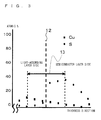
- Fig. 3 is a graph showing Cu distribution and S distribution extending from the semiconductor layer 4-side to the light-absorbing layer 3-side across the heterojunction interface 12 shown in Fig. 2 .
- the result of a quantitative analysis in atomic % in thickness direction indicates the presence of a region 13 in which Cu content decreases from the inside of the light-absorbing layer 3 to the heterojunction interface 12 and still decreases from the heterojunction interface 12 to the inside of the semiconductor layer 4.
- the CIGS (light-absorbing layer 3) shown in Figs. 2 and 3 includes Se (e.g., Cu(In, Ga)Se 2 and the like) as a group VIb element.
- a Cu-deficient portion is present locally in the one surface-side of the light-absorbing layer.
- the Cu-deficient portion has a high content of the at least one element selected from Cd, Zn, and In and a low content of Cu.
- the Cu-deficient portion 14 is a portion that has a relatively low Cu content on the surface-side of the light-absorbing layer 3 and that has a high content of at least one element selected from Cd, Zn, and In.
- unstable Cu is removed from the surface of the light-absorbing layer 3 and then replaced with the at least one element selected from the Cd, Zn, and In removed from the semiconductor layer 4 (e.g., CdS, ZnS, ZnO, In 2 S 3 , In 2 Se 3 , In 2 Te 3 and the like).
- the area of the heterojunction interface 12 substantially increases, which increases photoelectric conversion efficiency.
- the composition of the Cu-deficient portion 14 in the surface of the light-absorbing layer 3 is, for example, CuIn 3 Se 5 .
- the composition of portions other than the Cu-deficient portion 14 is, for example, Cu(In, Ga)Se 2 .
- the Cu-deficient portions 14 are preferably dispersed more finely throughout the surface of the light-absorbing layer 3 and more deeply from the surface of the light-absorbing layer 3 and preferably has a larger occupancy ratio in the surface of the light-absorbing layer 3 in order to substantially increase the area of the heterojunction interface 12.
- the photoelectric conversion efficiency cannot be increased by just simply increasing the surface roughness of the light-absorbing layer 3.
- the area of the heterojunction interface 12 can be increased more when the incomplete Cu compound is more abundantly present in the surface of the light-absorbing layer 3 as in the present invention.
- the heterojunction interface 12 in the Cu-deficient portion 14 is the solid line shown in Figs. 8 and 9 .
- the group VIb element included in the light-absorbing layer 3 includes Se and the group VIb element included in the semiconductor layer 4 includes S, and S content increases from the light-absorbing layer 3 to the semiconductor layer 4 across the junction interface 12.
- the S content increases from the inside of the light-absorbing layer 3 to the heterojunction interface 12 and still increases from the heterojunction interface 12 to the inside of the semiconductor layer 4.
- the plane orientation of the light-absorbing layer 3 is (112) and the plane orientation of the semiconductor layer 4 is (111).
- the plane orientation of the light-absorbing layer 3 is (112) and the plane orientation of the semiconductor layer 4 is (111) in this embodiment, a plane orientation other than (112) may be present on the light-absorbing layer 3 as long as the densities of the light-absorbing layer 3 and the semiconductor layer 4 are substantially equal to each other.
- the (111)-plane of the semiconductor layer 4 When the (111)-plane of the semiconductor layer 4 is grown on the (112)-plane of the light-absorbing layer 3, the (111)-plane of the semiconductor layer 4 can be observed in a TEM image taken so that the (112)-plane of the light-absorbing layer 3 can be observed.
- the position of the heterojunction interface 12 can be identified as a portion in the vicinity of the boundary of the light-absorbing layer 3 and the semiconductor layer 4 that have different plane orientations from each other.
- a photoelectric conversion module of an embodiment of the present invention includes a plurality of photoelectric conversion devices 10 and is formed by electrically connecting each of the photoelectric conversion devices 10 to the adjoining photoelectric conversion device 10.
- a photoelectric conversion module 11 can be prepared by sequentially arranging a plurality of the photoelectric conversion devices 10 and then electrically connecting the plurality of the photoelectric conversion devices 10 to one another.
- each photoelectric conversion device 10 includes a third electrode layer 6 formed on the substrate 1-side of a light-absorbing layer 3 so as to be spaced apart from a first electrode layer 2.
- a transparent electrode layer 5 and the third electrode layer 6 are electrically connected to each other with a connection conductor 7 formed on the light-absorbing layer 3.
- connection conductor 7 is preferably combined with the transparent electrode layer 5 to form a single piece by forming the connection conductor 7 at the same time of forming the transparent electrode layer 5. This allows the manufacturing process to be simplified and reliability of the electrical connection between the connection conductor 7 and the transparent electrode layer 5 to be enhanced.
- the connection conductor 7 connects between the transparent electrode layer 5 and the third electrode layer 6 and thereby allows each of the adjoining light-absorbing layers 3 to satisfactorily perform photoelectric conversion. As a result, current can be extracted through the connection conductor 7 in a series connection.
- the region in which Cu content decreases from the light-absorbing layer 3 to the semiconductor layer 4 across the junction interface 12 is a region extending 10 nm or more from the junction interface 12 in a direction perpendicular to the junction interface 12.
- the region 13 extends at least 10 nm or more from the heterojunction interface 12 to the light-absorbing layer 3-side and at least 10 nm or more from the heterojunction interface 12 to the semiconductor layer 4-side.
- the Cu-deficient portion 14 has an average width in a direction parallel to the junction interface 12 of 10 to 300 nm in a cross-sectional view of the light-absorbing layer 3 taken in its thickness direction.
- the Cu-deficient portion 14 has an average depth in a direction perpendicular to the junction interface 12 of 10 nm or more in a cross-sectional view of the light-absorbing layer 3 taken in its thickness direction.
- D and W denote the average depth and the average width, respectively.
- the Cu-deficient portion 14 has an occupancy ratio in the junction interface 12 of 10% or more in a cross-sectional view of the light-absorbing layer 3 taken in its thickness direction.
- the Cu-deficient portion 14 has an occupancy ratio of 10% or more in the heterojunction interface 12 in a perspective plan view of the light-absorbing layer 3 viewed from the semiconductor-layer 4-side.
- a method of manufacturing a photoelectric conversion device of the present embodiment includes a light-absorbing layer-forming step in which a light-absorbing layer is formed, the light-absorbing layer including a chalcopyrite-type compound containing a group Ib element including Cu, a group IIIb element, and a group VIb element, the light-absorbing layer including a Cu compound other than the chalcopyrite-type compound on a surface-side of the light-absorbing layer; and a thin film-forming step in which a thin film is formed on the light-absorbing layer by a wet deposition method while the light-absorbing layer is immersed in an acid solution or an alkali solution to cause elution of Cu from a surface of the light-absorbing layer, the thin film containing at least one element selected from Cd, Zn, and In and a group VIb element.
- the light-absorbing layer 3 comprised of a semiconductor may be formed by depositing a raw-material element by sputtering or vapor deposition in the form of a film or applying a raw-material solution in the form of a film to form a precursor containing the raw-material element and then heating the precursor.
- the light-absorbing layer 3 may be formed by forming, as a precursor, a film comprised of a metal element in the same manner as described above and then heating the precursor in a gas atmosphere containing a group VIb element.
- the method for forming the Cu compound other than the chalcopyrite-type compound on the surface-side of the light-absorbing layer 3 is not particularly limited.
- the Cu compound other than the chalcopyrite-type may be formed by, for example, mixing of the Cu compound other than the chalcopyrite-type near the final stage of the light-absorbing layer-forming step.
- a layer comprised of the Cu compound other than the chalcopyrite-type compound may be formed by mixing of a precursor containing Cu +1 such as copper hexafluoroacetylacetonate and then heating the resulting mixture at 100°C to 600°C.
- a precursor containing Cu +1 such as copper hexafluoroacetylacetonate
- a wet deposition method is employed.
- the wet deposition method used herein is a method in which a raw-material solution is applied to the light-absorbing layer 3 and then subjected to a heat treatment or the like to cause a chemical reaction or a method in which precipitation is performed on the light-absorbing layer 3 by a chemical reaction in a solution containing a raw material.
- Cu Since unreacted Cu and a Cu compound having an unstable composition are present as the Cu compound other than the chalcopyrite-type compound on the surface of the light-absorbing layer 3, Cu is caused to be easily eluted preferentially from the surface of the light-absorbing layer 3 due to the reaction with an acid solution or an alkali solution in the early stage of the thin film-forming step.
- porous holes are finely formed on the surface of the light-absorbing layer 3. Cu is considered to be eluted more easily through the holes.
- the semiconductor layer 4 is formed while incorporating the eluted Cu into the thin film.
- Cu content in the surface of the light-absorbing layer 3 becomes smaller than that in the entire portion of the light-absorbing layer 3. As a result, there is a tendency that Cu content decreases from the light-absorbing layer 3 to the semiconductor layer 4 across the junction interface 12.
Landscapes
- Photovoltaic Devices (AREA)
- Chemical & Material Sciences (AREA)
- Crystallography & Structural Chemistry (AREA)
- Life Sciences & Earth Sciences (AREA)
- Engineering & Computer Science (AREA)
- Sustainable Energy (AREA)
Abstract
Description
- The present invention relates to a photoelectric conversion device and a method of manufacturing the photoelectric conversion device.
- Photoelectric conversion devices have been required to have higher photoelectric conversion efficiency year after year. Such photoelectric conversion devices include a light-absorbing layer that is a CIS film or a CIGS film. A semiconductor layer that is to be stacked on the light-absorbing layer so as to form an optimal pn junction has been developed.
- For example, a method in which a high-resistivity thin film is interposed between the light-absorbing layer and the semiconductor layer in order to control a pn junction at the interface therebetween has been described (See Patent Literature 1).
-
- Patent Literature 1: Japanese Patent Application Laid-Open No.
8-271960 - However, in the photoelectric conversion device disclosed in
Patent Literature 1, the high-resistivity thin film formed in the vicinity of the junction interface between the light-absorbing layer and the semiconductor layer may increase series resistance. - In addition, the high-resistivity thin film interposed between the light-absorbing layer and the semiconductor layer may be a cause of disturbance to a pn junction in the vicinity of the junction interface between the light-absorbing layer and the semiconductor layer.
- Thus, it is difficult to consistently manufacture photoelectric conversion devices having high photoelectric conversion efficiency.
- A photoelectric conversion device of the present invention comprises a light-absorbing layer including a compound semiconductor capable of photoelectric conversion, the compound semiconductor containing a group Ib element including Cu, a group IIIb element and a group VIb element; and a semiconductor layer on one surface-side of the light-absorbing layer, the semiconductor layer having a plane orientation different from that of the light-absorbing layer, the semiconductor layer containing a group Ib element including Cu, at least one element selected from Cd, Zn and In and a group VIb element. The photoelectric conversion device includes a region in which Cu content decreases from the light-absorbing layer to the semiconductor layer across a junction interface.
- A method of manufacturing a photoelectric conversion device of the present invention comprises a light-absorbing layer-forming step in which a light-absorbing layer is formed, the light-absorbing layer including a chalcopyrite-type compound containing a group Ib element including Cu, a group IIIb element and a group VIb element, the light-absorbing layer including a Cu compound other than the chalcopyrite-type compound on a surface-side of the light-absorbing layer; and a thin film-forming step in which a thin film is formed on the light-absorbing layer by a wet deposition method while the light-absorbing layer is immersed in an acid solution or an alkali solution to cause elution of Cu from a surface of the light-absorbing layer, the thin film containing at least one element selected from Cd, Zn and In and a group VIb element.
- According to the present invention, the photoelectric conversion device includes a region in which Cu content decreases from the light-absorbing layer to the semiconductor layer across the junction interface. Therefore, the series resistance in the vicinity of the heterojunction interface does not change markedly and thus a photoelectric conversion device having stable conductivity and high photoelectric conversion efficiency can be manufactured.
-
- [
Fig. 1] Fig. 1 is a schematic cross-sectional view of a photoelectric conversion device of an embodiment according to the present invention. - [
Fig. 2] Fig. 2 is a photograph as a substitute for a drawing, which shows a portion in the vicinity of a heterojunction interface between a light-absorbing layer and a semiconductor layer of a photoelectric conversion device of an embodiment according to the present invention. - [
Fig. 3] Fig. 3 is a graph showing Cu and S concentration distributions in the vicinity of the heterojunction interface shown inFig. 2 . - [
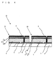
Fig. 4] Fig. 4 is a cross-sectional view showing an example of an embodiment of a photoelectric conversion apparatus and a photoelectric conversion module according to the present invention. - [
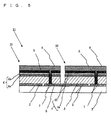
Fig. 5] Fig. 5 is a cross-sectional view showing another example of an embodiment of a photoelectric conversion apparatus and a photoelectric conversion module according to the present invention. - [
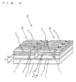
Fig. 6] Fig. 6 is a perspective view of the embodiment of the photoelectric conversion apparatus and the photoelectric conversion module according to the present invention shown inFig. 5 . - [
Fig. 7] Fig. 7 includes schematic diagrams illustrating a heterojunction interface of a photoelectric conversion device of an embodiment according to the present invention, whereFig. 7(a) is a plan view andFig. 7(b) is a cross-sectional perspective view. - [
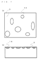
Fig. 8] Fig. 8 is a schematic cross-sectional view of a Cu-deficient portion in a photoelectric conversion device of an embodiment according to the present invention. - [
Fig. 9] Fig. 9 is an enlarged schematic cross-sectional view of the Cu-deficient portion shown inFig. 8 . Embodiments for Carrying Out the Invention - Hereafter, a photoelectric conversion device according to the present invention and a method of manufacturing the photoelectric conversion device according to the present invention will be described with reference to the attached drawings.
- As shown in
Fig. 1 , aphotoelectric conversion device 10 includes asubstrate 1, afirst electrode layer 2, a light-absorbinglayer 3, asemiconductor layer 4, and a second electrode layer 5 (hereafter, also referred to as transparent electrode layer 5). - The light-absorbing
layer 3 has the function of absorbing light and thereby generating electric charge. A chalcopyrite-type compound semiconductor is used as the light-absorbinglayer 3 because high photoelectric conversion efficiency is realized even when the light-absorbinglayer 3 has a small thickness of 10 µm or less. - Examples of the chalcopyrite-type compound semiconductor include Cu(In, Ga)Se2 (also referred to as CIGS), Cu(In, Ga)(Se, S)2 (also referred to as CIGSS), and CuInS2 (also referred to as CIS). Cu(In, Ga)Se2 is a compound mainly comprised of Cu, In, Ga, and Se. Cu(In, Ga) (Se, S)2 is a compound mainly comprised of Cu, In, Ga, Se, and S.
- In
Fig. 1 , thesemiconductor layer 4 is a layer forming a heterojunction with the light-absorbinglayer 3. - The
semiconductor layer 4 is formed on the light-absorbinglayer 3 and has a thickness of about 5 to 200 nm. The light-absorbinglayer 3 and thesemiconductor layer 4 preferably have different conductivity types from each other. For example, in the case where the light-absorbinglayer 3
is a p-type semiconductor, thesemiconductor layer 4 is an n-type semiconductor. Thesemiconductor layer 4 is preferably a layer having a resistivity of 1 Ω·cm or more in order to reduce leakage current. Thesemiconductor layer 4 preferably has optical transparency in the wavelength range of light absorbed by the light-absorbinglayer 3 in order to increase the absorption efficiency of the light-absorbinglayer 3. - The
semiconductor layer 4 preferably includes a compound of a group IIb element (e.g., Cd or Zn) or a group IIIb element (e.g., In) with a chalcogen (e.g., O, S, Se, or Te). - Specific examples of such a compound include CdS, ZnS, ZnO, In2S3, In2Se3, and In2Te3. In particular, In2S3, In2Se3, and In2Te3 have high durability and are less susceptible to degradation in a high-temperature, high-humidity environment. Therefore, both the high durability and high photoelectric conversion efficiency in a high-temperature, high-humidity environment are realized by stacking such a
semiconductor layer 4 on the light-absorbinglayer 3. - A gradient of the concentration of a specific element is present between the light-absorbing
layer 3 and thesemiconductor layer 4, which will be described below. - Moreover, even when a large-sized
photoelectric conversion device 10 is formed, in-plane variation of the above-described durability and photoelectric conversion efficiency can be suppressed. Thus, the size of aphotoelectric conversion device 10 having high durability and a good photoelectric conversion property can be increased. - The thickness of the
semiconductor layer 4 is preferably 5 to 100 nm. - When the thickness of the
semiconductor layer 4 is within the above-described range, band matching between thesemiconductor layer 4 and the light-absorbinglayer 3 is improved, and thus a charge-separation function of the photoelectric conversion portion constituted by the light-absorbinglayer 3 and thesemiconductor layer 4 can be enhanced. - As shown in
Fig. 4 , a plurality of thephotoelectric conversion devices 10 are arranged sequentially. - The
photoelectric conversion device 10 includes athird electrode layer 6 spaced apart from thefirst electrode layer 2 and formed on the substrate 1-side of the light-absorbinglayer 3. Thetransparent electrode layer 5 and thethird electrode layer 6 are electrically connected to each other with aconnection conductor 7 formed in the light-absorbinglayer 3. Thethird electrode layer 6 is integrated with afirst electrode layer 2 of the adjoiningphotoelectric conversion device 10. Thus, the adjoiningphotoelectric conversion devices 10 are connected to each other in series. In eachphotoelectric conversion device 10, theconnection conductor 7 is formed so as to penetrate the light-absorbinglayer 3 and thesemiconductor layer 4, and photoelectric conversion is carried out in the light-absorbinglayer 3 and thesemiconductor layer 4 that are interposed between thefirst electrode layer 2 and thetransparent electrode layer 5. - Although the
semiconductor layer 4 shown inFig. 2 has a single-layer structure, alternatively, a two-layered structure constituted by afirst semiconductor layer 4a and asecond semiconductor layer 4b that have different compositions from each other may be employed as shown inFigs. 4 to 6 . - In
Fig. 4 , thesubstrate 1 supports thephotoelectric conversion device 10. Examples of the material of thesubstrate 1 include glass, ceramic, resin, and metal. - In
Fig. 4 , thefirst electrode layer 2 and thethird electrode layer 6 are comprised of a conductive material such as Mo, Al, Ti, or Au and formed on thesubstrate 1 by a sputtering method, a vapor deposition method, or the like. - In
Fig. 4 , the second electrode (transparent electrode layer) 5 is a transparent conductive film comprised of ITO, ZnO, or the like having a thickness of 0.05 to 3 µm. Thetransparent electrode layer 5 is formed by a sputtering method, a vapor deposition method, a chemical vapor deposition (CVD) method, or the like. Thetransparent electrode layer 5 is a layer having a smaller resistivity than thesemiconductor layer 4, and electric charge generated in the light-absorbinglayer 3 is extracted through thetransparent electrode layer 5. The resistivity of thetransparent electrode layer 5 is preferably less than 1 Ω·cm and the sheet resistance of thetransparent electrode layer 5 is preferably 50 Ω/□ or less in order to satisfactorily extract the electric charge through thetransparent electrode layer 5. Thetransparent electrode layer 5 is preferably transparent to light absorbed by the light-absorbinglayer 3 in order to increase the absorption efficiency of the light-absorbinglayer 3. The thickness of thetransparent electrode layer 5 is preferably 0.05 to 0.5 µm in order to enhance a light-reflection-loss prevention effect and a light-scattering effect as well as optical transparency and in order to satisfactorily transmit current generated by photoelectric conversion. Thetransparent electrode layer 5 and thesemiconductor layer 4 preferably have the same refractive index as each other in order to prevent light-reflection loss from occurring at the junction interface between thetransparent electrode layer 5 and thesemiconductor layer 4. - Next, another embodiment of a photoelectric conversion device of the present invention is described with reference to
Figs. 5 and6 . -
Fig. 5 is a cross-sectional view of thephotoelectric conversion device 20 as another embodiment.Fig. 6 is a perspective view of thephotoelectric conversion device 20. Thephotoelectric conversion device 20 shown inFigs. 5 and6 is different from thephotoelectric conversion device 10 shown inFig. 4 in that acollector electrode 8 is formed on thetransparent electrode layer 5. InFigs. 5 and6 , the same portions as inFig. 4 are given the same reference numerals, and a plurality of thephotoelectric conversion devices 20 are connected to one another to form aphotoelectric conversion module 21 as in thephotoelectric conversion device 10 shown inFig. 4 . - Hereafter, an embodiment of the photoelectric conversion device of the present invention and another embodiment of the photoelectric conversion device of the present invention will be described in detail.
- The photoelectric conversion device of the present embodiment includes a light-absorbing layer including a compound semiconductor capable of photoelectric conversion, the compound semiconductor containing a group Ib element including Cu, a group IIIb element, and a group VIb element; and a semiconductor layer on one surface-side of the light-absorbing layer, the semiconductor layer having a plane orientation different from that of the light-absorbing layer, the semiconductor layer containing a group Ib element including Cu, at least one element selected from Cd, Zn, and In, and a group VIb element. The photoelectric conversion device has a region in which Cu content decreases from the light-absorbing layer to the semiconductor layer across a junction interface.
- As described above, examples of the
semiconductor layer 4 on the light-absorbinglayer 3 include chalcogenides of a group IIb element or a group IIIb element (e.g., CdS, ZnS, ZnO, In2S3, In2Se3, In2Te3 and the like). In the following description, In2S3 is used. -
Fig. 2 is a TEM image taken in the vicinity of aheterojunction interface 12 between the light-absorbinglayer 3 and thesemiconductor layer 4. The light-absorbinglayer 3 and thesemiconductor layer 4 have different plane orientations from each other, thus being distinguished from each other by theheterojunction interface 12 shown as a broken line. - The arrow in the upper-left direction in
Fig. 2 means that, during the manufacturing process described below, a portion of Cu eluted from the light-absorbinglayer 3 is embedded into thesemiconductor layer 4 and, on the other hand, a portion of In constituting thesemiconductor layer 4 is embedded into a site in the light-absorbinglayer 3 from which Cu is removed. - IN the case where the
semiconductor layer 4 is comprised of CdS or ZnS, a portion of Cd or Zn is embedded into the site in the light-absorbinglayer 3 from which Cu is removed. - Also, the arrow in the lower-right direction in
Fig. 2 means that a portion of S is removed from thesemiconductor layer 4 and then embedded throughout the entire surface of the light-absorbinglayer 3. -
Fig. 3 is a graph showing Cu distribution and S distribution extending from the semiconductor layer 4-side to the light-absorbing layer 3-side across theheterojunction interface 12 shown inFig. 2 . - As shown in
Figs. 2 and3 , the result of a quantitative analysis in atomic % in thickness direction indicates the presence of aregion 13 in which Cu content decreases from the inside of the light-absorbinglayer 3 to theheterojunction interface 12 and still decreases from theheterojunction interface 12 to the inside of thesemiconductor layer 4. - This prevents Cu content that has the most dominant influence on conductivity from being markedly changed in the vicinity of the
heterojunction interface 12 between the light-absorbinglayer 3 and thesemiconductor layer 4. Thus, series resistance is prevented from being markedly changed locally in the vicinity of theheterojunction interface 12. - As a result, the current loss in the vicinity of the
heterojunction interface 12 between the light-absorbinglayer 3 and thesemiconductor layer 4 is reduced, which increases the photoelectric conversion efficiency. - It is sufficient that the tendency that the Cu content decreases from the light-absorbing
layer 3 to thesemiconductor layer 4 across theheterojunction interface 12 between the light-absorbinglayer 3 and thesemiconductor layer 4 can be confirmed. Even if Cu content is increasing locally inside the light-absorbinglayer 3 or thesemiconductor layer 4, the increase in Cu content has little influence on the photoelectric conversion efficiency. - The CIGS (light-absorbing layer 3) shown in
Figs. 2 and3 includes Se (e.g., Cu(In, Ga)Se2 and the like) as a group VIb element. - In the photoelectric conversion device of the embodiment, a Cu-deficient portion is present locally in the one surface-side of the light-absorbing layer. The Cu-deficient portion has a high content of the at least one element selected from Cd, Zn, and In and a low content of Cu.
- As shown
Figs. 7 and8 , the Cu-deficient portion 14 is a portion that has a relatively low Cu content on the surface-side of the light-absorbinglayer 3 and that has a high content of at least one element selected from Cd, Zn, and In. - As shown in
Fig. 8 , unstable Cu is removed from the surface of the light-absorbinglayer 3 and then replaced with the at least one element selected from the Cd, Zn, and In removed from the semiconductor layer 4 (e.g., CdS, ZnS, ZnO, In2S3, In2Se3, In2Te3 and the like). As a result, the area of theheterojunction interface 12 substantially increases, which increases photoelectric conversion efficiency. - The composition of the Cu-
deficient portion 14 in the surface of the light-absorbinglayer 3 is, for example, CuIn3Se5. The composition of portions other than the Cu-deficient portion 14 is, for example, Cu(In, Ga)Se2. - The Cu-
deficient portions 14 are preferably dispersed more finely throughout the surface of the light-absorbinglayer 3 and more deeply from the surface of the light-absorbinglayer 3 and preferably has a larger occupancy ratio in the surface of the light-absorbinglayer 3 in order to substantially increase the area of theheterojunction interface 12. - Note that the important thing is not to just simply increase the area of the
junction interface 12 between thesemiconductor layer 4 and the light-absorbinglayer 3, but to increase the area of thejunction interface 12 at which a heterojunction is substantially formed. - Therefore, the photoelectric conversion efficiency cannot be increased by just simply increasing the surface roughness of the light-absorbing
layer 3. - This is because, when a light-absorbing
layer 3 having a certain surface roughness is used, the area of theheterojunction interface 12 can be increased more when the incomplete Cu compound is more abundantly present in the surface of the light-absorbinglayer 3 as in the present invention. - The
heterojunction interface 12 in the Cu-deficient portion 14 is the solid line shown inFigs. 8 and9 . - As shown in
Fig. 9 , Cu content decreases from the light-absorbinglayer 3 to thesemiconductor layer 4 even inside the Cu-deficient portion 14. - This is the same tendency as in a part of the
region 13 outside the Cu-deficient portion 14 in which Cu content decreases from the light-absorbinglayer 3 to thesemiconductor layer 4. - In the photoelectric conversion device according to the embodiment, the group VIb element included in the light-absorbing
layer 3 includes Se and the group VIb element included in thesemiconductor layer 4 includes S, and S content increases from the light-absorbinglayer 3 to thesemiconductor layer 4 across thejunction interface 12. - As shown in
Figs. 2 and3 , when being analyzed in the thickness direction in atomic %, the S content increases from the inside of the light-absorbinglayer 3 to theheterojunction interface 12 and still increases from theheterojunction interface 12 to the inside of thesemiconductor layer 4. - As a result, a good pn junction is formed at the
heterojunction interface 12 between the light-absorbinglayer 3 and thesemiconductor layer 4, which increases the photoelectric conversion efficiency. - It is sufficient that the tendency that the S content increases from the light-absorbing
layer 3 to thesemiconductor layer 4 across theheterojunction interface 12 between the light-absorbinglayer 3 and thesemiconductor layer 4 can be confirmed. Even if the S content is decreasing locally inside the light-absorbinglayer 3 or inside thesemiconductor layer 4, the decrease in S content has little influence on the photoelectric conversion efficiency. - Note that, in
Fig. 3 , In distribution is omitted and S distribution is shown. - In the photoelectric conversion device of the present embodiment, the plane orientation of the light-absorbing
layer 3 is (112) and the plane orientation of thesemiconductor layer 4 is (111). - This allows the densities of the light-absorbing
layer 3 and thesemiconductor layer 4 to be easily controlled to be substantially equal to each other and thereby prevents the absolute amounts of Cu and S from markedly varying across theheterojunction interface 12. - Although the plane orientation of the light-absorbing
layer 3 is (112) and the plane orientation of thesemiconductor layer 4 is (111) in this embodiment, a plane orientation other than (112) may be present on the light-absorbinglayer 3 as long as the densities of the light-absorbinglayer 3 and thesemiconductor layer 4 are substantially equal to each other. - When the (111)-plane of the
semiconductor layer 4 is grown on the (112)-plane of the light-absorbinglayer 3, the (111)-plane of thesemiconductor layer 4 can be observed in a TEM image taken so that the (112)-plane of the light-absorbinglayer 3 can be observed. - Thus, the position of the
heterojunction interface 12 can be identified as a portion in the vicinity of the boundary of the light-absorbinglayer 3 and thesemiconductor layer 4 that have different plane orientations from each other. - A photoelectric conversion module of an embodiment of the present invention includes a plurality of
photoelectric conversion devices 10 and is formed by electrically connecting each of thephotoelectric conversion devices 10 to the adjoiningphotoelectric conversion device 10. In other words, aphotoelectric conversion module 11 can be prepared by sequentially arranging a plurality of thephotoelectric conversion devices 10 and then electrically connecting the plurality of thephotoelectric conversion devices 10 to one another. - In order to easily connect the adjoining
photoelectric conversion devices 10 to one another in series, as shown inFig. 4 , eachphotoelectric conversion device 10 includes athird electrode layer 6 formed on the substrate 1-side of a light-absorbinglayer 3 so as to be spaced apart from afirst electrode layer 2. Atransparent electrode layer 5 and thethird electrode layer 6 are electrically connected to each other with aconnection conductor 7 formed on the light-absorbinglayer 3. - The
connection conductor 7 is preferably combined with thetransparent electrode layer 5 to form a single piece by forming theconnection conductor 7 at the same time of forming thetransparent electrode layer 5. This allows the manufacturing process to be simplified and reliability of the electrical connection between theconnection conductor 7 and thetransparent electrode layer 5 to be enhanced. Theconnection conductor 7 connects between thetransparent electrode layer 5 and thethird electrode layer 6 and thereby allows each of the adjoining light-absorbinglayers 3 to satisfactorily perform photoelectric conversion. As a result, current can be extracted through theconnection conductor 7 in a series connection. - In the photoelectric conversion device of the present embodiment, the region in which Cu content decreases from the light-absorbing
layer 3 to thesemiconductor layer 4 across thejunction interface 12 is a region extending 10 nm or more from thejunction interface 12 in a direction perpendicular to thejunction interface 12. - In
Fig. 8 , theregion 13 extends at least 10 nm or more from theheterojunction interface 12 to the light-absorbing layer 3-side and at least 10 nm or more from theheterojunction interface 12 to the semiconductor layer 4-side. - This allows Cu to be sufficiently diffused from the light-absorbing
layer 3 to thesemiconductor layer 4. As a result, an effective heterojunction is realized. - In the photoelectric conversion device of the present embodiment, the Cu-
deficient portion 14 has an average width in a direction parallel to thejunction interface 12 of 10 to 300 nm in a cross-sectional view of the light-absorbinglayer 3 taken in its thickness direction. - In the photoelectric conversion device of the present embodiment, the Cu-
deficient portion 14 has an average depth in a direction perpendicular to thejunction interface 12 of 10 nm or more in a cross-sectional view of the light-absorbinglayer 3 taken in its thickness direction. - In
Fig. 9 , D and W denote the average depth and the average width, respectively. When the average depth and the average width are within the above-described ranges, the area of theheterojunction interface 12 created by the Cu-deficient portion 14 can be efficiently increased. - In the photoelectric conversion device of the present embodiment, the Cu-
deficient portion 14 has an occupancy ratio in thejunction interface 12 of 10% or more in a cross-sectional view of the light-absorbinglayer 3 taken in its thickness direction. - This maintains the area of the
heterojunction interface 12 created by the Cu-deficient portion 14, which increases the photoelectric conversion efficiency. - It may be said in other words, the Cu-
deficient portion 14 has an occupancy ratio of 10% or more in theheterojunction interface 12 in a perspective plan view of the light-absorbinglayer 3 viewed from the semiconductor-layer 4-side. - In the observation of the Cu-
deficient portion 14, color mapping of the portion in the vicinity of the heterojunction interface 12 (region 13) on a TEM image allows a qualitative, quantitative observation to be easily made. - Next, the method of manufacturing the photoelectric conversion device of an embodiment of the present invention is described.
- A method of manufacturing a photoelectric conversion device of the present embodiment includes a light-absorbing layer-forming step in which a light-absorbing layer is formed, the light-absorbing layer including a chalcopyrite-type compound containing a group Ib element including Cu, a group IIIb element, and a group VIb element, the light-absorbing layer including a Cu compound other than the chalcopyrite-type compound on a surface-side of the light-absorbing layer; and a thin film-forming step in which a thin film is formed on the light-absorbing layer by a wet deposition method while the light-absorbing layer is immersed in an acid solution or an alkali solution to cause elution of Cu from a surface of the light-absorbing layer, the thin film containing at least one element selected from Cd, Zn, and In and a group VIb element.
- In the light-absorbing layer-forming step, the light-absorbing
layer 3 comprised of a semiconductor may be formed by depositing a raw-material element by sputtering or vapor deposition in the form of a film or applying a raw-material solution in the form of a film to form a precursor containing the raw-material element and then heating the precursor. - In another case, the light-absorbing
layer 3 may be formed by forming, as a precursor, a film comprised of a metal element in the same manner as described above and then heating the precursor in a gas atmosphere containing a group VIb element. - The method for forming the Cu compound other than the chalcopyrite-type compound on the surface-side of the light-absorbing
layer 3 is not particularly limited. - The Cu compound other than the chalcopyrite-type may be formed by, for example, mixing of the Cu compound other than the chalcopyrite-type near the final stage of the light-absorbing layer-forming step.
- Specifically, a layer comprised of the Cu compound other than the chalcopyrite-type compound may be formed by mixing of a precursor containing Cu+1 such as copper hexafluoroacetylacetonate and then heating the resulting mixture at 100°C to 600°C.
- In the thin film-forming step in which the
semiconductor layer 4 is formed, a wet deposition method is employed. - The wet deposition method used herein is a method in which a raw-material solution is applied to the light-absorbing
layer 3 and then subjected to a heat treatment or the like to cause a chemical reaction or a method in which precipitation is performed on the light-absorbinglayer 3 by a chemical reaction in a solution containing a raw material. - Since unreacted Cu and a Cu compound having an unstable composition are present as the Cu compound other than the chalcopyrite-type compound on the surface of the light-absorbing
layer 3, Cu is caused to be easily eluted preferentially from the surface of the light-absorbinglayer 3 due to the reaction with an acid solution or an alkali solution in the early stage of the thin film-forming step. - Therefore, porous holes are finely formed on the surface of the light-absorbing
layer 3. Cu is considered to be eluted more easily through the holes. - When the thin film containing at least one element selected from Cd, Zn, and In and a group VIb element is formed by a wet deposition method while Cu is eluted in an acid solution or an alkali solution as described above, the
semiconductor layer 4 is formed while incorporating the eluted Cu into the thin film. - Finally, Cu content in the surface of the light-absorbing
layer 3 becomes smaller than that in the entire portion of the light-absorbinglayer 3. As a result, there is a tendency that Cu content decreases from the light-absorbinglayer 3 to thesemiconductor layer 4 across thejunction interface 12. -
- 1: substrate
- 2: first electrode layer
- 3: light-absorbing layer
- 4: semiconductor layer
- 4a: first semiconductor layer
- 4b: second semiconductor layer
- 5: second electrode layer (transparent electrode layer)
- 6: third electrode layer
- 7: connection conductor
- 8: collector electrode
- 10: photoelectric conversion device
- 11: photoelectric conversion module
- 12: junction interface (heterojunction interface)
- 13: region
- 14: Cu-deficient portion
- 20: photoelectric conversion device
- 21: photoelectric conversion module
Claims (9)
- A photoelectric conversion device comprising:a light-absorbing layer including a compound semiconductor capable of photoelectric conversion, the compound semiconductor containing a group Ib element including Cu, a group IIIb element and a group VIb element; anda semiconductor layer on one surface-side of the light-absorbing layer, the semiconductor layer having a plane orientation different from that of the light-absorbing layer, the semiconductor layer containing a group Ib element including Cu, at least one element selected from Cd, Zn and In and a group VIb element,wherein the photoelectric conversion device includes a region in which Cu content decreases from the light-absorbing layer to the semiconductor layer across a junction interface.
- The photoelectric conversion device according to Claim 1, wherein a Cu-deficient portion is present locally in the one surface-side of the light-absorbing layer, the Cu-deficient portion including a high content of the at least one element selected from Cd, Zn and In and a low content of Cu.
- The photoelectric conversion device according to Claim 1 or 2, wherein the group VIb element included in the light-absorbing layer includes Se and the group VIb element included in the semiconductor layer includes S,
wherein S content increases from the light-absorbing layer to the semiconductor layer across the junction interface. - The photoelectric conversion device according to any one of Claims 1 to 3, wherein the light-absorbing layer has a plane orientation of (112) and the semiconductor layer has a plane orientation of (111).
- The photoelectric conversion device according to any one of Claims 1 to 4, wherein the region extends 10 nm or more from the junction interface in a direction perpendicular to the junction interface.
- The photoelectric conversion device according to any one of Claims 2 to 5, wherein the Cu-deficient portion has an average width in a direction parallel to the junction interface of 10 to 300 nm in a cross-sectional view of the light-absorbing layer taken in its thickness direction.
- The photoelectric conversion device according to any one of Claims 2 to 6, wherein the Cu-deficient portion has an average depth in a direction perpendicular to the junction interface of 10 nm or more in a cross-sectional view of the light-absorbing layer taken in its thickness direction.
- The photoelectric conversion device according to any one of Claims 2 to 7, wherein the Cu-deficient portion has an occupancy ratio in the junction interface of 10% or more in a cross-sectional view of the light-absorbing layer taken in its thickness direction.
- A method of manufacturing a photoelectric conversion device, the method comprising:a light-absorbing layer-forming step in which a light-absorbing layer is formed, the light-absorbing layer including a chalcopyrite-type compound containing a group Ib element including Cu, a group IIIb element and a group VIb element, the light-absorbing layer including a Cu compound other than the chalcopyrite-type compound on a surface-side of the light-absorbing layer; anda thin film-forming step in which a thin film is formed on the light-absorbing layer by a wet deposition method while the light-absorbing layer is immersed in an acid solution or an alkali solution to cause elution of Cu from a surface of the light-absorbing layer, the thin film containing at least one element selected from Cd, Zn and In and a group VIb element.
Applications Claiming Priority (2)
| Application Number | Priority Date | Filing Date | Title |
|---|---|---|---|
| JP2011121874 | 2011-05-31 | ||
| PCT/JP2012/063978 WO2012165500A1 (en) | 2011-05-31 | 2012-05-30 | Photoelectric conversion element and method for producing same |
Publications (2)
| Publication Number | Publication Date |
|---|---|
| EP2717326A1 true EP2717326A1 (en) | 2014-04-09 |
| EP2717326A4 EP2717326A4 (en) | 2014-12-03 |
Family
ID=47259352
Family Applications (1)
| Application Number | Title | Priority Date | Filing Date |
|---|---|---|---|
| EP12793480.0A Withdrawn EP2717326A4 (en) | 2011-05-31 | 2012-05-30 | PHOTOELECTRIC CONVERSION ELEMENT AND METHOD FOR PRODUCING THE SAME |
Country Status (4)
| Country | Link |
|---|---|
| US (1) | US9064993B2 (en) |
| EP (1) | EP2717326A4 (en) |
| JP (1) | JP5730391B2 (en) |
| WO (1) | WO2012165500A1 (en) |
Families Citing this family (3)
| Publication number | Priority date | Publication date | Assignee | Title |
|---|---|---|---|---|
| US9431562B2 (en) * | 2014-01-21 | 2016-08-30 | Taiwan Semiconductor Manufacturing Co., Ltd. | Three dimensional compositional profile in CIS-based absorber layers of thin film solar cells |
| US9653628B2 (en) * | 2014-03-10 | 2017-05-16 | Taiwan Semiconductor Manufacturing Co., Ltd. | Absorber layer for photovoltaic device, and method of making the same |
| JP2017059657A (en) * | 2015-09-16 | 2017-03-23 | 株式会社東芝 | Photoelectric conversion element and solar cell |
Family Cites Families (6)
| Publication number | Priority date | Publication date | Assignee | Title |
|---|---|---|---|---|
| JP3181074B2 (en) | 1991-07-16 | 2001-07-03 | 松下電器産業株式会社 | Method for producing Cu-based chalcopyrite film |
| JP3414814B2 (en) | 1994-01-24 | 2003-06-09 | 松下電器産業株式会社 | Solar cell and manufacturing method thereof |
| JPH08271960A (en) | 1995-03-29 | 1996-10-18 | Nikon Corp | Camera with frame shift prevention function |
| DE69734183T8 (en) | 1996-10-15 | 2007-03-29 | Matsushita Electric Industrial Co., Ltd., Kadoma | Solar cell and manufacturing process |
| JP3646953B2 (en) | 1996-10-15 | 2005-05-11 | 松下電器産業株式会社 | Solar cell |
| JP2012079727A (en) * | 2010-09-30 | 2012-04-19 | Kyocera Corp | Photoelectric conversion element and method for manufacturing the same |
-
2012
- 2012-05-30 JP JP2013518134A patent/JP5730391B2/en active Active
- 2012-05-30 EP EP12793480.0A patent/EP2717326A4/en not_active Withdrawn
- 2012-05-30 WO PCT/JP2012/063978 patent/WO2012165500A1/en not_active Ceased
- 2012-05-30 US US14/113,109 patent/US9064993B2/en not_active Expired - Fee Related
Non-Patent Citations (8)
| Title |
|---|
| ABOU-RAS D ET AL: "Interfacial layer formations between Cu(In,Ga)Se2 and InxSy layers", JOURNAL OF APPLIED PHYSICS, AMERICAN INSTITUTE OF PHYSICS, US, vol. 98, no. 12, 27 December 2005 (2005-12-27), pages 123512-1-123512-7, XP012078012, ISSN: 0021-8979, DOI: 10.1063/1.2149166 * |
| ABOU-RAS D ET AL: "Microstructural and chemical studies of interfaces between Cu(In,Ga)Se2 and In2S3 layers", JOURNAL OF APPLIED PHYSICS, AMERICAN INSTITUTE OF PHYSICS, US, vol. 97, no. 8, 5 April 2005 (2005-04-05), pages 084908-1-084908-8, XP012071143, ISSN: 0021-8979, DOI: 10.1063/1.1863454 * |
| ABOU-RAS D ET AL: "Structural and chemical investigations of CBD- and PVD-CdS buffer layers and interfaces in Cu(In,Ga)Se2-based thin film solar cells", THIN SOLID FILMS, ELSEVIER-SEQUOIA S.A. LAUSANNE, CH, vol. 480-481, 1 June 2005 (2005-06-01), pages 118-123, XP027865207, ISSN: 0040-6090 [retrieved on 2005-06-01] * |
| LEI C ET AL: "Effects of solution-grown CdS on Cu(InGa)Se2 grain boundaries", JOURNAL OF APPLIED PHYSICS, AMERICAN INSTITUTE OF PHYSICS, US, vol. 108, no. 11, 9 December 2010 (2010-12-09), pages 114908-1-114908-6, XP012142145, ISSN: 0021-8979, DOI: 10.1063/1.3512966 * |
| See also references of WO2012165500A1 * |
| SHIMAKAWA S-I ET AL: "Annealing effects on Zn1-xMgxO/CIGS interfaces characterized by ultraviolet light excited time-resolved photoluminescence", SOLAR ENERGY MATERIALS AND SOLAR CELLS, ELSEVIER SCIENCE PUBLISHERS, AMSTERDAM, NL, vol. 92, no. 9, 6 May 2008 (2008-05-06), pages 1086-1090, XP022735455, ISSN: 0927-0248, DOI: 10.1016/J.SOLMAT.2008.03.014 [retrieved on 2008-05-06] * |
| WADA T ET AL: "High-efficiency CIGS solar cells with modified CIGS surface", SOLAR ENERGY MATERIALS AND SOLAR CELLS, ELSEVIER SCIENCE PUBLISHERS, AMSTERDAM, NL, vol. 67, no. 1-4, 1 March 2001 (2001-03-01), pages 305-310, XP004224775, ISSN: 0927-0248, DOI: 10.1016/S0927-0248(00)00296-8 * |
| William N Shafarman ET AL: "Cu(InGa)Se2 Solar Cells" In: "Handbook of Photovoltaic Science and Engineering, Second Edition", 21 December 2010 (2010-12-21), John Wiley & Sons, Ltd, Chichester, UK, XP055113329, vol. 18, pages 546-599, DOI: doi/10.1002/9780470974704.ch13, * page 566, paragraph 2 - page 567, paragraph 1 * * |
Also Published As
| Publication number | Publication date |
|---|---|
| WO2012165500A1 (en) | 2012-12-06 |
| JPWO2012165500A1 (en) | 2015-02-23 |
| EP2717326A4 (en) | 2014-12-03 |
| US20140042580A1 (en) | 2014-02-13 |
| JP5730391B2 (en) | 2015-06-10 |
| US9064993B2 (en) | 2015-06-23 |
Similar Documents
| Publication | Publication Date | Title |
|---|---|---|
| US20080023059A1 (en) | Tandem solar cell structures and methods of manufacturing same | |
| US20130008496A1 (en) | Solar cell apparatus and manufacturing method thereof | |
| CN104011875B (en) | Solaode and manufacture method thereof | |
| US8916905B2 (en) | Photoelectric conversion device | |
| JP2013506991A (en) | Photovoltaic power generation apparatus and manufacturing method thereof | |
| KR101154654B1 (en) | Solar cell apparatus and method of fabricating the same | |
| US9064993B2 (en) | Photoelectric conversion device and method of manufacturing photoelectric conversion device | |
| KR101231364B1 (en) | Solar cell and method of fabircating the same | |
| US20130299829A1 (en) | Photoelectric conversion device | |
| JP5642005B2 (en) | PHOTOELECTRIC CONVERSION DEVICE, ITS MANUFACTURING METHOD, AND PHOTOELECTRIC CONVERSION MODULE | |
| KR20120086217A (en) | Solar cell apparatus and method of fabricating the same | |
| JP5918765B2 (en) | Solar power plant | |
| KR20110043358A (en) | Solar cell and manufacturing method thereof | |
| Mollica et al. | Assessment of Indium‐Free Transparent Conductive Oxide Back Contacts for High‐Efficiency Ultra‐Thin Cu (In, Ga) Se2 Solar Cells Down to 250 nm | |
| CN102473768A (en) | Solar cell and manufacturing method thereof | |
| KR101034146B1 (en) | Solar cell and manufacturing method thereof | |
| JP5784125B2 (en) | Method for manufacturing photoelectric conversion element | |
| KR101327102B1 (en) | Solar cell and method of fabricating the same | |
| KR101173429B1 (en) | Solar cell and method of fabircating the same | |
| US20140352772A1 (en) | Solar cell and method of manufacturing the same | |
| US20160240700A1 (en) | Solar Battery | |
| KR101231398B1 (en) | Solar cell apparatus and method of fabricating the same | |
| KR101273123B1 (en) | Solar cell apparatus and method of fabricating the same | |
| JP2014022562A (en) | Method for manufacturing photoelectric conversion device | |
| JP2012054261A (en) | Photoelectric conversion device, method of manufacturing the same, and photoelectric conversion module |
Legal Events
| Date | Code | Title | Description |
|---|---|---|---|
| PUAI | Public reference made under article 153(3) epc to a published international application that has entered the european phase |
Free format text: ORIGINAL CODE: 0009012 |
|
| 17P | Request for examination filed |
Effective date: 20131024 |
|
| AK | Designated contracting states |
Kind code of ref document: A1 Designated state(s): AL AT BE BG CH CY CZ DE DK EE ES FI FR GB GR HR HU IE IS IT LI LT LU LV MC MK MT NL NO PL PT RO RS SE SI SK SM TR |
|
| DAX | Request for extension of the european patent (deleted) | ||
| A4 | Supplementary search report drawn up and despatched |
Effective date: 20141030 |
|
| RIC1 | Information provided on ipc code assigned before grant |
Ipc: H01L 31/0749 20120101AFI20141024BHEP Ipc: H01L 31/032 20060101ALI20141024BHEP |
|
| GRAP | Despatch of communication of intention to grant a patent |
Free format text: ORIGINAL CODE: EPIDOSNIGR1 |
|
| INTG | Intention to grant announced |
Effective date: 20180108 |
|
| RIN1 | Information on inventor provided before grant (corrected) |
Inventor name: KUROSU, KEITA Inventor name: OOMAE, SATOSHI |
|
| STAA | Information on the status of an ep patent application or granted ep patent |
Free format text: STATUS: THE APPLICATION HAS BEEN WITHDRAWN |
|
| 18W | Application withdrawn |
Effective date: 20180418 |