EP2716792A1 - Process for the manufacture of local nanostructures of high purity material - Google Patents
Process for the manufacture of local nanostructures of high purity material Download PDFInfo
- Publication number
- EP2716792A1 EP2716792A1 EP12187384.8A EP12187384A EP2716792A1 EP 2716792 A1 EP2716792 A1 EP 2716792A1 EP 12187384 A EP12187384 A EP 12187384A EP 2716792 A1 EP2716792 A1 EP 2716792A1
- Authority
- EP
- European Patent Office
- Prior art keywords
- metal
- process according
- molecules
- deposition
- ion
- Prior art date
- Legal status (The legal status is an assumption and is not a legal conclusion. Google has not performed a legal analysis and makes no representation as to the accuracy of the status listed.)
- Withdrawn
Links
- 238000000034 method Methods 0.000 title claims abstract description 51
- 230000008569 process Effects 0.000 title claims abstract description 38
- 239000000463 material Substances 0.000 title description 8
- 239000002086 nanomaterial Substances 0.000 title description 7
- 238000004519 manufacturing process Methods 0.000 title description 6
- 229910052751 metal Inorganic materials 0.000 claims abstract description 29
- 239000002184 metal Substances 0.000 claims abstract description 29
- 230000008021 deposition Effects 0.000 claims abstract description 24
- 239000002243 precursor Substances 0.000 claims abstract description 23
- 239000012530 fluid Substances 0.000 claims abstract description 21
- 239000000758 substrate Substances 0.000 claims abstract description 14
- 238000010884 ion-beam technique Methods 0.000 claims abstract description 13
- 239000002245 particle Substances 0.000 claims abstract description 11
- 229910044991 metal oxide Inorganic materials 0.000 claims abstract description 8
- 150000004706 metal oxides Chemical class 0.000 claims abstract description 8
- 229910052739 hydrogen Inorganic materials 0.000 claims abstract description 7
- 229910052760 oxygen Inorganic materials 0.000 claims abstract description 7
- UFHFLCQGNIYNRP-UHFFFAOYSA-N Hydrogen Chemical compound [H][H] UFHFLCQGNIYNRP-UHFFFAOYSA-N 0.000 claims abstract description 6
- 239000001257 hydrogen Substances 0.000 claims abstract description 6
- 239000001301 oxygen Substances 0.000 claims abstract description 6
- -1 oxygen ions Chemical class 0.000 claims abstract description 5
- 230000001678 irradiating effect Effects 0.000 claims abstract description 3
- BASFCYQUMIYNBI-UHFFFAOYSA-N platinum Substances [Pt] BASFCYQUMIYNBI-UHFFFAOYSA-N 0.000 claims description 13
- XEEYBQQBJWHFJM-UHFFFAOYSA-N Iron Chemical compound [Fe] XEEYBQQBJWHFJM-UHFFFAOYSA-N 0.000 claims description 11
- 150000002500 ions Chemical class 0.000 claims description 11
- POILWHVDKZOXJZ-ARJAWSKDSA-M (z)-4-oxopent-2-en-2-olate Chemical compound C\C([O-])=C\C(C)=O POILWHVDKZOXJZ-ARJAWSKDSA-M 0.000 claims description 10
- KDLHZDBZIXYQEI-UHFFFAOYSA-N Palladium Chemical group [Pd] KDLHZDBZIXYQEI-UHFFFAOYSA-N 0.000 claims description 10
- 150000002736 metal compounds Chemical class 0.000 claims description 9
- PXHVJJICTQNCMI-UHFFFAOYSA-N Nickel Chemical compound [Ni] PXHVJJICTQNCMI-UHFFFAOYSA-N 0.000 claims description 7
- 239000010949 copper Substances 0.000 claims description 7
- QGHDLJAZIIFENW-UHFFFAOYSA-N 4-[1,1,1,3,3,3-hexafluoro-2-(4-hydroxy-3-prop-2-enylphenyl)propan-2-yl]-2-prop-2-enylphenol Chemical group C1=C(CC=C)C(O)=CC=C1C(C(F)(F)F)(C(F)(F)F)C1=CC=C(O)C(CC=C)=C1 QGHDLJAZIIFENW-UHFFFAOYSA-N 0.000 claims description 6
- 150000004696 coordination complex Chemical class 0.000 claims description 6
- 125000000058 cyclopentadienyl group Chemical group C1(=CC=CC1)* 0.000 claims description 6
- 229910052742 iron Inorganic materials 0.000 claims description 6
- YDNLRUSAWWOAFZ-UHFFFAOYSA-N C[Pt]C1C=CC=C1 Chemical compound C[Pt]C1C=CC=C1 YDNLRUSAWWOAFZ-UHFFFAOYSA-N 0.000 claims description 5
- 229910052802 copper Inorganic materials 0.000 claims description 5
- 229910052763 palladium Inorganic materials 0.000 claims description 5
- AUFHQOUHGKXFEM-UHFFFAOYSA-N C[Au]C Chemical compound C[Au]C AUFHQOUHGKXFEM-UHFFFAOYSA-N 0.000 claims description 4
- 125000004432 carbon atom Chemical group C* 0.000 claims description 4
- ZSWFCLXCOIISFI-UHFFFAOYSA-N endo-cyclopentadiene Natural products C1C=CC=C1 ZSWFCLXCOIISFI-UHFFFAOYSA-N 0.000 claims description 4
- 230000004907 flux Effects 0.000 claims description 4
- 239000010931 gold Substances 0.000 claims description 4
- 229910052697 platinum Inorganic materials 0.000 claims description 4
- RYGMFSIKBFXOCR-UHFFFAOYSA-N Copper Chemical compound [Cu] RYGMFSIKBFXOCR-UHFFFAOYSA-N 0.000 claims description 3
- 229910052737 gold Inorganic materials 0.000 claims description 3
- 229910052759 nickel Inorganic materials 0.000 claims description 3
- GKNMBVVJQTWDRT-UHFFFAOYSA-N 2,2,6,6-tetramethylheptane Chemical compound CC(C)(C)CCCC(C)(C)C GKNMBVVJQTWDRT-UHFFFAOYSA-N 0.000 claims description 2
- 125000005595 acetylacetonate group Chemical group 0.000 claims description 2
- 125000000217 alkyl group Chemical group 0.000 claims description 2
- 229910052782 aluminium Inorganic materials 0.000 claims description 2
- 229910052804 chromium Inorganic materials 0.000 claims description 2
- 239000011651 chromium Substances 0.000 claims description 2
- 229910052758 niobium Inorganic materials 0.000 claims description 2
- 229910052702 rhenium Inorganic materials 0.000 claims description 2
- 229910052703 rhodium Inorganic materials 0.000 claims description 2
- 239000010948 rhodium Substances 0.000 claims description 2
- 229910052707 ruthenium Inorganic materials 0.000 claims description 2
- 229910052709 silver Inorganic materials 0.000 claims description 2
- 229910052719 titanium Inorganic materials 0.000 claims description 2
- 229910052721 tungsten Inorganic materials 0.000 claims description 2
- 238000000151 deposition Methods 0.000 description 21
- 238000000313 electron-beam-induced deposition Methods 0.000 description 12
- OKTJSMMVPCPJKN-UHFFFAOYSA-N Carbon Chemical compound [C] OKTJSMMVPCPJKN-UHFFFAOYSA-N 0.000 description 7
- 229910052799 carbon Inorganic materials 0.000 description 7
- 238000001888 ion beam-induced deposition Methods 0.000 description 7
- 239000007789 gas Substances 0.000 description 6
- VYPSYNLAJGMNEJ-UHFFFAOYSA-N Silicium dioxide Chemical compound O=[Si]=O VYPSYNLAJGMNEJ-UHFFFAOYSA-N 0.000 description 5
- BOTDANWDWHJENH-UHFFFAOYSA-N Tetraethyl orthosilicate Chemical compound CCO[Si](OCC)(OCC)OCC BOTDANWDWHJENH-UHFFFAOYSA-N 0.000 description 4
- 238000006243 chemical reaction Methods 0.000 description 4
- 238000000354 decomposition reaction Methods 0.000 description 4
- 230000006872 improvement Effects 0.000 description 4
- 239000000203 mixture Substances 0.000 description 4
- 239000000126 substance Substances 0.000 description 4
- WZJUBBHODHNQPW-UHFFFAOYSA-N 2,4,6,8-tetramethyl-1,3,5,7,2$l^{3},4$l^{3},6$l^{3},8$l^{3}-tetraoxatetrasilocane Chemical compound C[Si]1O[Si](C)O[Si](C)O[Si](C)O1 WZJUBBHODHNQPW-UHFFFAOYSA-N 0.000 description 3
- 229910021012 Co2(CO)8 Inorganic materials 0.000 description 3
- QVGXLLKOCUKJST-UHFFFAOYSA-N atomic oxygen Chemical compound [O] QVGXLLKOCUKJST-UHFFFAOYSA-N 0.000 description 3
- 238000010894 electron beam technology Methods 0.000 description 3
- 239000007787 solid Substances 0.000 description 3
- 229910008940 W(CO)6 Inorganic materials 0.000 description 2
- 230000008901 benefit Effects 0.000 description 2
- 238000012512 characterization method Methods 0.000 description 2
- 238000005229 chemical vapour deposition Methods 0.000 description 2
- 229910052681 coesite Inorganic materials 0.000 description 2
- 150000001875 compounds Chemical class 0.000 description 2
- 238000004590 computer program Methods 0.000 description 2
- 229910052906 cristobalite Inorganic materials 0.000 description 2
- 238000010438 heat treatment Methods 0.000 description 2
- 230000003993 interaction Effects 0.000 description 2
- 239000007788 liquid Substances 0.000 description 2
- 230000003647 oxidation Effects 0.000 description 2
- 238000007254 oxidation reaction Methods 0.000 description 2
- 230000000704 physical effect Effects 0.000 description 2
- 239000000377 silicon dioxide Substances 0.000 description 2
- 241000894007 species Species 0.000 description 2
- 229910052682 stishovite Inorganic materials 0.000 description 2
- 238000003860 storage Methods 0.000 description 2
- 229910052905 tridymite Inorganic materials 0.000 description 2
- GMAAWMLLGOGZQO-UHFFFAOYSA-N C1(C=CC=C1)[Pt]C1C=CC=C1 Chemical compound C1(C=CC=C1)[Pt]C1C=CC=C1 GMAAWMLLGOGZQO-UHFFFAOYSA-N 0.000 description 1
- GNNIIYWMEZVVSP-UHFFFAOYSA-N C[Pt]C1=CC=CC1 Chemical compound C[Pt]C1=CC=CC1 GNNIIYWMEZVVSP-UHFFFAOYSA-N 0.000 description 1
- MYMOFIZGZYHOMD-UHFFFAOYSA-N Dioxygen Chemical compound O=O MYMOFIZGZYHOMD-UHFFFAOYSA-N 0.000 description 1
- PXGOKWXKJXAPGV-UHFFFAOYSA-N Fluorine Chemical compound FF PXGOKWXKJXAPGV-UHFFFAOYSA-N 0.000 description 1
- 229910001218 Gallium arsenide Inorganic materials 0.000 description 1
- 235000010627 Phaseolus vulgaris Nutrition 0.000 description 1
- 244000046052 Phaseolus vulgaris Species 0.000 description 1
- 229910052581 Si3N4 Inorganic materials 0.000 description 1
- QXZUUHYBWMWJHK-UHFFFAOYSA-N [Co].[Ni] Chemical compound [Co].[Ni] QXZUUHYBWMWJHK-UHFFFAOYSA-N 0.000 description 1
- 230000004075 alteration Effects 0.000 description 1
- 239000012472 biological sample Substances 0.000 description 1
- 239000013590 bulk material Substances 0.000 description 1
- 239000006227 byproduct Substances 0.000 description 1
- 229910002091 carbon monoxide Inorganic materials 0.000 description 1
- CVCSGXJPONFHRC-UHFFFAOYSA-N carbon monoxide;cobalt;nitroxyl anion Chemical compound [Co].[O+]#[C-].[O+]#[C-].[O+]#[C-].O=[N-] CVCSGXJPONFHRC-UHFFFAOYSA-N 0.000 description 1
- 150000001728 carbonyl compounds Chemical class 0.000 description 1
- 125000002915 carbonyl group Chemical group [*:2]C([*:1])=O 0.000 description 1
- 239000000919 ceramic Substances 0.000 description 1
- 230000008859 change Effects 0.000 description 1
- 229910017052 cobalt Inorganic materials 0.000 description 1
- 239000010941 cobalt Substances 0.000 description 1
- GUTLYIVDDKVIGB-UHFFFAOYSA-N cobalt atom Chemical compound [Co] GUTLYIVDDKVIGB-UHFFFAOYSA-N 0.000 description 1
- CYXIENZYTDFIFC-UHFFFAOYSA-N cobalt iron Chemical compound [Fe].[Fe].[Co] CYXIENZYTDFIFC-UHFFFAOYSA-N 0.000 description 1
- JPNWDVUTVSTKMV-UHFFFAOYSA-N cobalt tungsten Chemical compound [Co].[W] JPNWDVUTVSTKMV-UHFFFAOYSA-N 0.000 description 1
- 238000011109 contamination Methods 0.000 description 1
- 238000001816 cooling Methods 0.000 description 1
- XPPWAISRWKKERW-UHFFFAOYSA-N copper palladium Chemical compound [Cu].[Pd] XPPWAISRWKKERW-UHFFFAOYSA-N 0.000 description 1
- 238000005137 deposition process Methods 0.000 description 1
- 229910001882 dioxygen Inorganic materials 0.000 description 1
- 238000010494 dissociation reaction Methods 0.000 description 1
- 230000005593 dissociations Effects 0.000 description 1
- 238000005530 etching Methods 0.000 description 1
- 238000005243 fluidization Methods 0.000 description 1
- 239000011737 fluorine Substances 0.000 description 1
- 229910052731 fluorine Inorganic materials 0.000 description 1
- 230000006870 function Effects 0.000 description 1
- 239000011521 glass Substances 0.000 description 1
- 238000003384 imaging method Methods 0.000 description 1
- 238000002347 injection Methods 0.000 description 1
- 239000007924 injection Substances 0.000 description 1
- 150000002739 metals Chemical class 0.000 description 1
- 238000002156 mixing Methods 0.000 description 1
- 150000002902 organometallic compounds Chemical class 0.000 description 1
- ZONODCCBXBRQEZ-UHFFFAOYSA-N platinum tungsten Chemical compound [W].[Pt] ZONODCCBXBRQEZ-UHFFFAOYSA-N 0.000 description 1
- 229920000642 polymer Polymers 0.000 description 1
- 238000000746 purification Methods 0.000 description 1
- 230000005855 radiation Effects 0.000 description 1
- 230000001105 regulatory effect Effects 0.000 description 1
- 230000004044 response Effects 0.000 description 1
- 239000011163 secondary particle Substances 0.000 description 1
- 239000004065 semiconductor Substances 0.000 description 1
- 229910052710 silicon Inorganic materials 0.000 description 1
- 239000010703 silicon Substances 0.000 description 1
- 235000012239 silicon dioxide Nutrition 0.000 description 1
- 229910052814 silicon oxide Inorganic materials 0.000 description 1
- 238000000859 sublimation Methods 0.000 description 1
- 230000008022 sublimation Effects 0.000 description 1
- 238000006467 substitution reaction Methods 0.000 description 1
- 238000005979 thermal decomposition reaction Methods 0.000 description 1
- 230000000007 visual effect Effects 0.000 description 1
- 235000012431 wafers Nutrition 0.000 description 1
- XLYOFNOQVPJJNP-UHFFFAOYSA-N water Chemical compound O XLYOFNOQVPJJNP-UHFFFAOYSA-N 0.000 description 1
Images
Classifications
-
- C—CHEMISTRY; METALLURGY
- C23—COATING METALLIC MATERIAL; COATING MATERIAL WITH METALLIC MATERIAL; CHEMICAL SURFACE TREATMENT; DIFFUSION TREATMENT OF METALLIC MATERIAL; COATING BY VACUUM EVAPORATION, BY SPUTTERING, BY ION IMPLANTATION OR BY CHEMICAL VAPOUR DEPOSITION, IN GENERAL; INHIBITING CORROSION OF METALLIC MATERIAL OR INCRUSTATION IN GENERAL
- C23C—COATING METALLIC MATERIAL; COATING MATERIAL WITH METALLIC MATERIAL; SURFACE TREATMENT OF METALLIC MATERIAL BY DIFFUSION INTO THE SURFACE, BY CHEMICAL CONVERSION OR SUBSTITUTION; COATING BY VACUUM EVAPORATION, BY SPUTTERING, BY ION IMPLANTATION OR BY CHEMICAL VAPOUR DEPOSITION, IN GENERAL
- C23C16/00—Chemical coating by decomposition of gaseous compounds, without leaving reaction products of surface material in the coating, i.e. chemical vapour deposition [CVD] processes
- C23C16/44—Chemical coating by decomposition of gaseous compounds, without leaving reaction products of surface material in the coating, i.e. chemical vapour deposition [CVD] processes characterised by the method of coating
- C23C16/48—Chemical coating by decomposition of gaseous compounds, without leaving reaction products of surface material in the coating, i.e. chemical vapour deposition [CVD] processes characterised by the method of coating by irradiation, e.g. photolysis, radiolysis, particle radiation
- C23C16/486—Chemical coating by decomposition of gaseous compounds, without leaving reaction products of surface material in the coating, i.e. chemical vapour deposition [CVD] processes characterised by the method of coating by irradiation, e.g. photolysis, radiolysis, particle radiation using ion beam radiation
Definitions
- the present invention relates to a process for the manufacture of local nanostructures of high purity metal or metal oxide and to nanostructures obtained with it.
- the invention relates to deposited metal or metal oxide in local nanostructures, the relevant parameters of interest of which (e.g. resistivity) do not deviate too much from related bulk properties of the same metal.
- EBID electron beam induced deposition
- IBID ion beam induced deposition
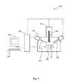
- a charged particle beam system 300 is schematically shown for use in the process of the present invention.
- the system 300 comprises:
- the work piece 110 to receive the deposited layer is selected depending on the application and purpose of the deposition.
- semiconductor wafers of silicon, Si3N4, GaAs or Ge may be used.
- Other possibilities include biological samples, polymers, glass (SiO2) and ceramics.
- the internal system environment is typically regulated in some way to reduce the risk of contamination and to reduce interaction between the charged particle beam and atmospheric gasses.
- a reduced pressure may be used or even vacuum, vacuum levels being typically less than 10 -5 mbar or better.
- the fluid injector 390 typically comprises a control system to regulate the flow of the deposition fluid, and one or more guides inside the system 300 to ensure that a desired partial pressure of deposition fluid is achieved at the irradiation position.
- a capillary tube having a small orifice is used to direct the fluid towards the work piece.
- the point of delivery may be made adjustable by incorporating manipulators.
- the further configuration of the fluid injector 390 depends upon the fluid to be injected - it may comprise cooling and/or heating to achieve a certain temperature, it may comprise a reservoir for containing the deposition fluid or it may be in communication with a remote supply, it may comprise pressurization means to achieve a certain deposition gas pressure or flow rate.
- precursor compound for injection depends mainly upon the material to be deposited. However, other important criteria include the ability to create a fluid form at reasonable temperatures, adequate adhesion of the deposited material to the work piece, stability at the fluidic temperature and the production of relatively few by-products.
- the molecules Once injected, the molecules will temporarily adhere to the surface and within that residence time they may interact with electrons supplied by the electron beam or electrons generated by the impinging beam.
- This interaction results in a decomposition of the precursor molecule into a volatile part, such as CO or a CH 4 group (that is pumped away by the vacuum system), and a deposition part, which forms nanostructures on the substrate.
- a volatile part such as CO or a CH 4 group
- images may be produced using the deposited material.
- a mask may be used to impart a pattern into beam for imaging on the work piece.
- the precursor material may be gas, liquid or solid. Liquid or solids are typically gasified prior to deposition, usually through fluidization or sublimation, and introduced, at accurately controlled rate, into the system chamber. Alternatively, solid precursor may be sublimated by the irradiation using a charged beam.
- the local flux of molecules is in the order of 10 15 -10 19 molecules/cm 2 .s, while beam currents are in the range from 50 pA to 1 nA. It is generally assumed that the secondary electrons with an energy ⁇ 50 eV, emitted from the substrate, are the main contributors to the decomposition process.
- IBID Ion Beam Induced Deposition
- Typical for the creation of a metallic structure is a precursor based organo-metallic compound, the fluid of which is used as a gas supply to the system. Many of these chemicals resemble the chemicals used in chemical vapor deposition (CVD) based processes, where decomposition is driven by collisions with the substrate at high temperatures (thermal decomposition).
- CVD chemical vapor deposition
- Said applied techniques offered an overall improvement but may also cause new undesired problems such as release of fluorine and the corresponding etching.
- MeCpPtMe 3 can be regarded as a standard platinum precursor.
- the reaction of its decomposition can be depicted by C 9 H 16 Pt + electrons ⁇ C 5 Pt + 4CH 4 + electrons which after pump out of the CH 4 actually results in around 16 at% of Pt.
- Heating the substrate up to 300°C did not change the chemical composition within the error bandwidth as the residual carbon cannot escape from the deposited metal, even if it might be released by breaking its chemical bond. This means that there is no volatility unless it can bind to, for example, oxygen or hydrogen to form CO, CO 2 or CH 4 respectively. In other words, the particular balance is missing. The same may be concluded for Me 2 Auacac, for Pd(hfac) 2 and Cu(hfac) 2 and Ni(Cp) 2 as is known from the literature.
- Au(CO)Cl a > 95 at% Au can be obtained, while both Cl and CO are volatile components.
- the actual reaction is quite simple: for example Co 2 (CO) 8 + electrons ⁇ 2Co + 8CO + electrons, and CO is fully volatile.
- low resistivity is meant a resistivity of less than 120 ⁇ .cm and preferably of less than 50 ⁇ .cm.
- an object of the present invention is to provide said improved process.
- Another object of the present invention is to provide deposited nano metal layers on shaped articles, showing improved relevant physical properties, in particular a resistivity of less than 120 ⁇ .cm and preferably less than 50 ⁇ .cm. More preferably the deposited material is Ohmic or has a resistivity of within a factor 5 of the bulk metal.
- an IBID process for the deposition of nano layers comprising a direct supply from the focused ion beam (FIB) of hydrogen or oxygen (further indicated as hydrogen FIB or oxygen FIB respectively).
- FIB focused ion beam
- the present invention relates to a process for deposition of high purity metal or metal oxide nano layers, comprising directing a precursor fluid toward a substrate surface, and irradiating the substrate surface with a focused ion beam in the presence of the precursor fluid, the precursor fluid dissociating in the presence of the particle beam to deposit a metal on the substrate surface, characterized in that the focused ion bean comprises hydrogen or oxygen ions.
- the precursor consists of a metal compound or metal complex, wherein at least a part of the carbon atoms are straightly bound to other carbon atoms,
- the metal compound or metal complex comprises one or more alkyl groups, acetyl acetonate groups, cyclopentadienyl groups, ⁇ -diketonate groups, 2,2,6,6-tetramethyl heptane dionate groups or combinations thereof.
- Preferred metals to be deposited can be selected from Al, Ag, Au, Co, Cr, Cu, Fe, Ge, Mo, Nb, Ni, Os, Pd, Pt, Rh, Ru, Re, Ti and W.
- Preferred metal oxides to be deposited are ZnO and SnO.
- Preferred examples of such a metal compound or metal complex are selected from the group consisiting of palladium hexafluoro acetylacetonate, copper hexafluoro acetylacetonate, nickel di(cyclopentadienyl), iron di(cyclopentadienyl, methyl cyclopentadienyl platinum trimethyl, dimethyl gold acetylacetonate and di(cyclopentadienyl) platinum.
- metal compounds are methyl cyclopentadienyl platinum trimethyl and dimethyl gold acetylacetonate.
- the deposited metal has a resistivity of less than 120 ⁇ .cm and more preferably of less than 50 ⁇ .cm.
- the deposited metal is Ohmic or has a resistivity within a factor of 5 of the bulk material.
- methyl cyclopentadienyl platinum trimethyl can be converted along the equation PtC 9 H 16 + 20 ⁇ H ⁇ 9CH 4 + Pt in which the Pt is substantially pure.
- the split into volatile and nonvolatile species can be exactly according to the particle balance as CO is split off and pumped away.
- W(CO) 6 the split is not ideal and remainders of mainly carbon can stay in the deposition.
- the H or O ions supplied from the ion beam can assist in removal of the remaining carbon (H) and removal of the remaining carbon in addition to full oxidation of the metal (O). So the beams have in this case the advantage of providing additional purification (H) or full oxidation (O) to the oxide form of the metal included.
- the process applies for H+ ion beams a yield for deposition in the range of from 0,05 molecules/ion, and still more preferably from 0,1 molecules/ion to 2,0 molecules/ion, while for O ++ ion beams a yield for deposition is used in the range of from 0.5 to 10 molecules/ion
- an ion beam is used, which has energy in the range of from 0.2 keV to 50 keV and more preferably in the range of from 0.5 to 30 keV.
- a local flux of molecules in the order of 10 16 molecules/cm 2 .s is applied while beam currents are used in the range of from 50 pA to 50 nA and preferably from 0.5 to 10 nA.
- Another aspect of the present invention is formed by shaped nano layers of high purity metal, obtainable by the hereinbefore specified process of the invention.
- embodiments of the present invention can be implemented via computer hardware, a combination of both hardware and software, or by computer instructions stored in a non-transitory computer-readable memory.
- the methods can be implemented in computer programs using standard programming techniques-including a non-transitory computer-readable storage medium configured with a computer program, where the storage medium so configured causes a computer to operate in a specific and predefined manner.
- Each program may be implemented in a high level procedural or object oriented programming language to communicate with a computer system.
- the programs can be implemented in assembly or machine language, if desired. In any case, the language can be a compiled or interpreted language.
- the program can run on dedicated integrated circuits programmed for that purpose.
Landscapes
- Chemical & Material Sciences (AREA)
- Health & Medical Sciences (AREA)
- Toxicology (AREA)
- General Chemical & Material Sciences (AREA)
- Chemical Kinetics & Catalysis (AREA)
- Engineering & Computer Science (AREA)
- Materials Engineering (AREA)
- Mechanical Engineering (AREA)
- Metallurgy (AREA)
- Organic Chemistry (AREA)
- Electrodes Of Semiconductors (AREA)
Abstract
A process for deposition of high purity metal or metal oxide nano layers comprising:
directing a precursor fluid toward a substrate surface, and irradiating the substrate surface with a focused ion beam in the presence of the precursor fluid, the precursor fluid dissociating in the presence of the particle beam to deposit a metal or metal oxide on the substrate surface, characterized in that the focused ion beam comprises hydrogen or oxygen ions, and shaped nano layers of high purity metal obtainable by said process.
directing a precursor fluid toward a substrate surface, and irradiating the substrate surface with a focused ion beam in the presence of the precursor fluid, the precursor fluid dissociating in the presence of the particle beam to deposit a metal or metal oxide on the substrate surface, characterized in that the focused ion beam comprises hydrogen or oxygen ions, and shaped nano layers of high purity metal obtainable by said process.
Description
- The present invention relates to a process for the manufacture of local nanostructures of high purity metal or metal oxide and to nanostructures obtained with it.
- More in particular the invention relates to deposited metal or metal oxide in local nanostructures, the relevant parameters of interest of which (e.g. resistivity) do not deviate too much from related bulk properties of the same metal.
- For a long time already several companies are trying to develop electron beam induced deposition (EBID) and ion beam induced deposition (IBID) techniques to create local nanostructures of metal.
- These techniques can be used for the direct creation of a nanostructure in 2 or 3 dimensions.
- In
Figure 1 , a chargedparticle beam system 300 is schematically shown for use in the process of the present invention. Thesystem 300 comprises: - a
charged particle column 310 generating a focusedbeam 360 of charged particles so as to irradiate a work piece110; - a
detector 350 for detecting radiation emanating from thework piece 110 in response to the irradiation with the focused beam, for example a detector for secondary electrons emitted from the work piece due to the impingement of an electron or ion beam. This may be used for characterization of the deposition during or after deposition. Alternatively, or in addition, thedetector 350 may comprise an X-ray detector so that the EDX technique may be used for elemental characterization in combination with an appropriate particle beam setting.; - a
fluid injector 390 feeding a fluid, typically a gas, to the proximity of thework piece 110 surface; - a work piece holder 380 for receiving and positioning the
work piece 110; - a
control apparatus 320 to control the internal system environment, movement of thework piece holder 380, the chargedparticle beam source 310, thefluid injector 390, and to process signals from thedetector 350; - a
user interface 330 for providing user input, and - a
display 340 for providing the user with visual information. - The
work piece 110 to receive the deposited layer is selected depending on the application and purpose of the deposition. For example, semiconductor wafers of silicon, Si3N4, GaAs or Ge may be used. Other possibilities include biological samples, polymers, glass (SiO2) and ceramics. - The internal system environment is typically regulated in some way to reduce the risk of contamination and to reduce interaction between the charged particle beam and atmospheric gasses. For example, a reduced pressure may be used or even vacuum, vacuum levels being typically less than 10-5 mbar or better.
- The
fluid injector 390 typically comprises a control system to regulate the flow of the deposition fluid, and one or more guides inside thesystem 300 to ensure that a desired partial pressure of deposition fluid is achieved at the irradiation position. For example, a capillary tube having a small orifice is used to direct the fluid towards the work piece. The point of delivery may be made adjustable by incorporating manipulators. - The further configuration of the
fluid injector 390 depends upon the fluid to be injected - it may comprise cooling and/or heating to achieve a certain temperature, it may comprise a reservoir for containing the deposition fluid or it may be in communication with a remote supply, it may comprise pressurization means to achieve a certain deposition gas pressure or flow rate. - The choice of precursor compound for injection depends mainly upon the material to be deposited. However, other important criteria include the ability to create a fluid form at reasonable temperatures, adequate adhesion of the deposited material to the work piece, stability at the fluidic temperature and the production of relatively few by-products.
- Once injected, the molecules will temporarily adhere to the surface and within that residence time they may interact with electrons supplied by the electron beam or electrons generated by the impinging beam.
- This interaction results in a decomposition of the precursor molecule into a volatile part, such as CO or a CH4 group (that is pumped away by the vacuum system), and a deposition part, which forms nanostructures on the substrate.
- By appropriate scanning of the beam during deposition, images may be produced using the deposited material. Alternatively a mask may be used to impart a pattern into beam for imaging on the work piece. These techniques are well known in the art.
- The precursor material may be gas, liquid or solid. Liquid or solids are typically gasified prior to deposition, usually through fluidization or sublimation, and introduced, at accurately controlled rate, into the system chamber. Alternatively, solid precursor may be sublimated by the irradiation using a charged beam.
- Typically the local flux of molecules is in the order of 1015-1019 molecules/cm2.s, while beam currents are in the range from 50 pA to 1 nA. It is generally assumed that the secondary electrons with an energy < 50 eV, emitted from the substrate, are the main contributors to the decomposition process.
- Ion Beam Induced Deposition (IBID) is very similar to EBID, with the mayor difference that a focused ion beam, usually 30 to 40 keV Ga+, is used instead of the electron beam.
- In both techniques it is not the primary beam but the secondary particles (secondary electrons), which cause the deposition. Said processes were known from e.g. Wikipedia "Electron beam induced deposition".
- Typical for the creation of a metallic structure is a precursor based organo-metallic compound, the fluid of which is used as a gas supply to the system. Many of these chemicals resemble the chemicals used in chemical vapor deposition (CVD) based processes, where decomposition is driven by collisions with the substrate at high temperatures (thermal decomposition).
- Examples of precursor materials that are regularly and frequently used for EBID are listed in the next Table:
Precursor short name/formula deposition Methyl cyclo-pentadienyl platinum trimethyl MeCpPtMe3 platinum Tungsten hexacarbonyl W(CO)6 tungsten Cobalt octacarbonyl Co2(CO)8 cobalt Tetra ethyl ortho silicate TEOS SiO2 Dimethyl gold acetyl acetonate Me2Auacac gold 2,4,6,8-tetramethyl cyclotetrasiloxane TMCTS SiOx Copper hexafluoro acetyl acetonate Cu(hfac)2 copper Palladium hexafluoro acetyl acetonate Pd(hfac)2 palladium Nickel dicyclopentadienyl Ni(Cp)2 nickel Cobalt tricarbonyl nitrosyl Co(CO)3NO cobalt Di iron nona carbonyl Fe2(CO)9 iron - So far the success for EBID and IBID has been limited due to the generally low purity of the deposited metal. This low purity of the metal deposit sets a limit to the applicability. Even if the purity of the deposited metal is not too bad, the relevant parameter (e.g. resistivity) can deviate too much from related bulk properties (for example a factor 100 or 1000), such that application becomes difficult if not impossible.
- A variety of strategies have been applied to enhance said purity and improve the local properties: gas mixing as TEOS (tetraethylorthosilicate) with water vapor or TMCTS (tetramethylcyclotetrasiloxane) with oxygen gas, the choice of precursor types away from carbon containing metal compounds or complexes (such as Pt(PF3)4) work at elevated substrate temperatures (e.g. improvement of W deposition from 35 at% to 55 at%).
- Said applied techniques offered an overall improvement but may also cause new undesired problems such as release of fluorine and the corresponding etching.
- One of the basic reasons for the lack of high purity has been the inability to create sufficient volatile molecules during the deposition process.
- For example: MeCpPtMe3 can be regarded as a standard platinum precursor. The reaction of its decomposition can be depicted by
C9H16Pt + electrons → C5Pt + 4CH4 + electrons
which after pump out of the CH4 actually results in around 16 at% of Pt. - Heating the substrate up to 300°C did not change the chemical composition within the error bandwidth as the residual carbon cannot escape from the deposited metal, even if it might be released by breaking its chemical bond. This means that there is no volatility unless it can bind to, for example, oxygen or hydrogen to form CO, CO2 or CH4 respectively. In other words, the particular balance is missing. The same may be concluded for Me2Auacac, for Pd(hfac)2 and Cu(hfac)2 and Ni(Cp)2 as is known from the literature.
- More in particular, processes using one of the precursors were known from e.g. Nanotechnology, 2011, Feb.4 22(5), Mulders J.J., Belova, L.M., Riazanova, A; Functional Nanoscience, Beilstein Symposium, May 17-21, 2010, Bozen, Italy, Towards Electron Beam Induced Deposition; Improvements for Nanotechnology, Mulders, J.J.L and Botman, A, published June 13, 2011.
- The best results obtained so far are for Fe2(CO)9 and for Co2(CO)8 where it is possible to get 78 at% Fe and 100 at% Co respectively.
- Also for Au(CO)Cl a > 95 at% Au can be obtained, while both Cl and CO are volatile components. Here the actual reaction is quite simple: for example Co2(CO)8 + electrons → 2Co + 8CO + electrons, and CO is fully volatile.
- It will be appreciated that one of the main causes for low purity are the missing species to create volatile molecules.
- It will be appreciated by persons skilled in this field of art, that in an electron beam induced deposition (EBID) process these molecules will have to be present in large quantities at the position of the deposition. In other words: in high densities. However, a local supply will not be easy and will require a very high flux to and hence a large chamber pressure increase and in the case of gas additional dissociation processes will be required before reaction with a precursor becomes effective.
- Therefore there is still a need for an improved, highly efficient IBID or EBID process, resulting in high purity deposited nano layers showing improved relevant physical properties, such as a low resistivity, on shaped articles, and which can apply almost all carbon based precursors, which normally leave non volatile carbon-containing compounds behind in de deposition itself.
- With the term "low resistivity" is meant a resistivity of less than 120 µΩ.cm and preferably of less than 50 µΩ.cm.
- Therefore an object of the present invention is to provide said improved process.
- Another object of the present invention is to provide deposited nano metal layers on shaped articles, showing improved relevant physical properties, in particular a resistivity of less than 120 µΩ.cm and preferably less than 50 µΩ.cm. More preferably the deposited material is Ohmic or has a resistivity of within a factor 5 of the bulk metal.
- As a result of extensive research and experimentation, an IBID process for the deposition of nano layers has surprisingly been found, comprising a direct supply from the focused ion beam (FIB) of hydrogen or oxygen (further indicated as hydrogen FIB or oxygen FIB respectively).
- Accordingly the present invention relates to a process for deposition of high purity metal or metal oxide nano layers, comprising directing a precursor fluid toward a substrate surface, and irradiating the substrate surface with a focused ion beam in the presence of the precursor fluid, the precursor fluid dissociating in the presence of the particle beam to deposit a metal on the substrate surface, characterized in that the focused ion bean comprises hydrogen or oxygen ions.
- According to a preferred embodiment of the process of the present invention, the precursor consists of a metal compound or metal complex, wherein at least a part of the carbon atoms are straightly bound to other carbon atoms,
- According to a more preferred embodiment of the present invention, the metal compound or metal complex comprises one or more alkyl groups, acetyl acetonate groups, cyclopentadienyl groups, β-diketonate groups, 2,2,6,6-tetramethyl heptane dionate groups or combinations thereof.
- Preferred metals to be deposited can be selected from Al, Ag, Au, Co, Cr, Cu, Fe, Ge, Mo, Nb, Ni, Os, Pd, Pt, Rh, Ru, Re, Ti and W.
- Preferred metal oxides to be deposited are ZnO and SnO.
- Preferred examples of such a metal compound or metal complex are selected from the group consisiting of palladium hexafluoro acetylacetonate, copper hexafluoro acetylacetonate, nickel di(cyclopentadienyl), iron di(cyclopentadienyl, methyl cyclopentadienyl platinum trimethyl, dimethyl gold acetylacetonate and di(cyclopentadienyl) platinum.
- More preferred examples of metal compounds are methyl cyclopentadienyl platinum trimethyl and dimethyl gold acetylacetonate.
- According to a more preferred embodiment of the present invention the deposited metal has a resistivity of less than 120 µΩ.cm and more preferably of less than 50 µΩ.cm.
- Still more preferably the deposited metal is Ohmic or has a resistivity within a factor of 5 of the bulk material.
- For example, according to a specific preferred embodiment of the method of the present invention methyl cyclopentadienyl platinum trimethyl can be converted along the equation
PtC9H16 + 20·H → 9CH4 + Pt
in which the Pt is substantially pure. - The same result can also be reached via
PtC9H16 + 9O2 → 9CO2 + 8H2 + Pt or
- PtC9H16 + 5O2 → 5CO2 + 4CH4 + Pt, and reactions in between these two.
- It is noted that for carbonyl compounds the split into volatile and nonvolatile species can be exactly according to the particle balance as CO is split off and pumped away. However, it should be noted that in many cases (e.g. W(CO)6) the split is not ideal and remainders of mainly carbon can stay in the deposition. In that case the H or O ions supplied from the ion beam can assist in removal of the remaining carbon (H) and removal of the remaining carbon in addition to full oxidation of the metal (O). So the beams have in this case the advantage of providing additional purification (H) or full oxidation (O) to the oxide form of the metal included.
- According to specific embodiments the present invention the process applies for H+ ion beams a yield for deposition in the range of from 0,05 molecules/ion, and still more preferably from 0,1 molecules/ion to 2,0 molecules/ion, while for O++ ion beams a yield for deposition is used in the range of from 0.5 to 10 molecules/ion According to other specific embodiments of the present invention an ion beam is used, which has energy in the range of from 0.2 keV to 50 keV and more preferably in the range of from 0.5 to 30 keV.
- In the process of the present invention a local flux of molecules in the order of 1016 molecules/cm2.s is applied while beam currents are used in the range of from 50 pA to 50 nA and preferably from 0.5 to 10 nA.
- It will be appreciated that another aspect of the present invention is formed by shaped nano layers of high purity metal, obtainable by the hereinbefore specified process of the invention.
- Although the description of the present invention above is mainly directed at methods for beam-induced deposition of low-resistivity material, it should be recognized that an apparatus performing the operation of such a method would further be within the scope of the present invention. Further, it should be recognized that embodiments of the present invention can be implemented via computer hardware, a combination of both hardware and software, or by computer instructions stored in a non-transitory computer-readable memory. The methods can be implemented in computer programs using standard programming techniques-including a non-transitory computer-readable storage medium configured with a computer program, where the storage medium so configured causes a computer to operate in a specific and predefined manner. Each program may be implemented in a high level procedural or object oriented programming language to communicate with a computer system. However, the programs can be implemented in assembly or machine language, if desired. In any case, the language can be a compiled or interpreted language. Moreover, the program can run on dedicated integrated circuits programmed for that purpose.
- Although the present invention and its advantages have been described in detail, it should be understood that various changes, substitutions, and alterations can be made to the embodiments described herein without departing from the scope of the invention as defined by the appended claims. Moreover, the scope of the present application is not intended to be limited to the particular embodiments of the process, machine, manufacture, composition of matter, means, methods and steps described in the specification. As one of ordinary skill in the art will readily appreciate from the disclosure of the present invention, processes, machines, manufacture, compositions of matter, means, methods, or steps, presently existing or later to be developed that perform substantially the same function or achieve substantially the same result as the corresponding embodiments described herein may be utilized according to the present invention. Accordingly, the appended claims are intended to include within their scope such processes, machines, manufacture, compositions of matter, means, methods, or steps.
- Wikipedia: "Electron beam induced deposition" Nanotechnology, 2011, Feb.4 22(5), Mulders J.J., Belova, L.M., Riazanova, A Functional Nanoscience, Beilstein Symposium, May 17-21, 2010, Bozen, Italy, Towards Electron Beam Induced Deposition; Improvements for Nanotechnology, Mulders, J.J.L and Botman, A, published June 13, 2011.
Claims (15)
- A process for deposition of high purity metal or metal oxide nano layers comprising:directing a precursor fluid toward a substrate surface, and irradiating the substrate surface with a focused ion beam in the presence of the precursor fluid, the precursor fluid dissociating in the presence of the particle beam to deposit a metal or metal oxide on the substrate surface, characterized in that the focused ion beam comprises hydrogen or oxygen ions.
- A process according to claim 1, in which the precursor consists of a metal compound or metal complex, wherein at least a part of the carbon atoms are straightly bound to other carbon atoms.
- A process according to the claims 1 and 2, in which the metal compound or metal complex comprises one or more alkyl groups, acetyl acetonate groups, cyclopentadienyl groups, β-diketonate groups, 2,2,6,6-tetramethyl heptane dionate groups or combinations thereof.
- Process according to claim 3, wherein the metal compound or metal complex is selected from the group consisting of palladium hexafluoro acetyl acetonate, copper hexafluoro acetyl acetonate, nickel di(cyclopentadienyl), iron di(cyclopentadienyl), methyl cyclopentadienyl platinum trimethyl, dimethyl gold acetylacetonate and dicyclopentadienyl platinum.
- Process according to claims 1-4, wherein the metal compound is methyl cyclopentadienyl platinum trimethyl or dimethyl gold acetyl.
- Process according to the claims 1-5, wherein the metal to be deposited can be selected from Al, Ag, Au, Co, Cr, Cu, Fe, Ge, Mo, Nb, Ni, Os, Pd, Pt, Rh, Ru, Re, Ti and W.
- Process according to claim 1, wherein the deposited metal has a resistivity of less than 120 µΩ.cm.
- Process according to claim 7, wherein the deposited metal has a resistivity of less than 50 µΩ.cm.
- Process according to claim 1, wherein the deposited metal is Ohmic or has a resistivity within a factor 5 of the bulk metal.
- Process according to claim 1, wherein the yield for deposition for H+ ions is in the range of from 0,05 molecules/ion to 2,5 molecules/ion, and more preferably in the range of from 0,1 molecules/ion to 2,0 molecules/ion.
- Process according to claim 1, wherein an ion beam, having an energy in the range of from 0,2 keV to 50 keV, is used.
- Process according to claim 1, wherein the local flux of molecules is in the order of 1015-1019 molecules/cm2.
- Process according to claim 1, wherein the beam currents are in the range of from 50 pA to 50 nA.
- Shaped nanolayers of high purity metal obtainable by the process of any of the claims 1-13.
- A charged particle beam system configured and arranged to perform the process of claims 1-13.
Priority Applications (1)
| Application Number | Priority Date | Filing Date | Title |
|---|---|---|---|
| EP12187384.8A EP2716792A1 (en) | 2012-10-05 | 2012-10-05 | Process for the manufacture of local nanostructures of high purity material |
Applications Claiming Priority (1)
| Application Number | Priority Date | Filing Date | Title |
|---|---|---|---|
| EP12187384.8A EP2716792A1 (en) | 2012-10-05 | 2012-10-05 | Process for the manufacture of local nanostructures of high purity material |
Publications (1)
| Publication Number | Publication Date |
|---|---|
| EP2716792A1 true EP2716792A1 (en) | 2014-04-09 |
Family
ID=47191506
Family Applications (1)
| Application Number | Title | Priority Date | Filing Date |
|---|---|---|---|
| EP12187384.8A Withdrawn EP2716792A1 (en) | 2012-10-05 | 2012-10-05 | Process for the manufacture of local nanostructures of high purity material |
Country Status (1)
| Country | Link |
|---|---|
| EP (1) | EP2716792A1 (en) |
Cited By (1)
| Publication number | Priority date | Publication date | Assignee | Title |
|---|---|---|---|---|
| US10538844B2 (en) | 2015-09-11 | 2020-01-21 | Fei Company | Nanofabrication using a new class of electron beam induced surface processing techniques |
Citations (3)
| Publication number | Priority date | Publication date | Assignee | Title |
|---|---|---|---|---|
| EP1160826A2 (en) * | 2000-05-30 | 2001-12-05 | Ebara Corporation | Coating, modification and etching of substrate surface with particle beam irradiation |
| US6627268B1 (en) * | 2001-05-03 | 2003-09-30 | Novellus Systems, Inc. | Sequential ion, UV, and electron induced chemical vapor deposition |
| US6758900B1 (en) * | 1999-10-07 | 2004-07-06 | Nec Corporation | Micro three-dimensional structure, production method therefor and production device therefor |
-
2012
- 2012-10-05 EP EP12187384.8A patent/EP2716792A1/en not_active Withdrawn
Patent Citations (3)
| Publication number | Priority date | Publication date | Assignee | Title |
|---|---|---|---|---|
| US6758900B1 (en) * | 1999-10-07 | 2004-07-06 | Nec Corporation | Micro three-dimensional structure, production method therefor and production device therefor |
| EP1160826A2 (en) * | 2000-05-30 | 2001-12-05 | Ebara Corporation | Coating, modification and etching of substrate surface with particle beam irradiation |
| US6627268B1 (en) * | 2001-05-03 | 2003-09-30 | Novellus Systems, Inc. | Sequential ion, UV, and electron induced chemical vapor deposition |
Non-Patent Citations (5)
| Title |
|---|
| FUNCTIONAL NANOSCIENCE, BEILSTEIN SYMPOSIUM, 17 May 2010 (2010-05-17) |
| JOVANOVI Z ET AL: "Platinum deposition from hydrogen-ion beam irradiated solid precursor", MATERIALS LETTERS, NORTH HOLLAND PUBLISHING COMPANY. AMSTERDAM, NL, vol. 65, no. 17, 3 May 2011 (2011-05-03), pages 2655 - 2657, XP028237370, ISSN: 0167-577X, [retrieved on 20110601], DOI: 10.1016/J.MATLET.2011.05.015 * |
| MULDERS J.J.; BELOVA, L.M.; RIAZANOVA, A, NANOTECHNOLOGY, vol. 22, no. 5, 4 February 2011 (2011-02-04) |
| MULDERS, J.J.L; BOTMAN, A, IMPROVEMENTS FOR NANOTECHNOLOGY, 13 June 2011 (2011-06-13) |
| ZHU J ET AL: "Growth and properties of amorphous Ge:H solar cells", JOURNAL OF NON-CRYSTALLINE SOLIDS, NORTH-HOLLAND PHYSICS PUBLISHING. AMSTERDAM, NL, vol. 338-340, 15 June 2004 (2004-06-15), pages 651 - 654, XP004514671, ISSN: 0022-3093, DOI: 10.1016/J.JNONCRYSOL.2004.03.072 * |
Cited By (2)
| Publication number | Priority date | Publication date | Assignee | Title |
|---|---|---|---|---|
| US10538844B2 (en) | 2015-09-11 | 2020-01-21 | Fei Company | Nanofabrication using a new class of electron beam induced surface processing techniques |
| US11377740B2 (en) | 2015-09-11 | 2022-07-05 | Fei Company | Nanofabrication using a new class of electron beam induced surface processing techniques |
Similar Documents
| Publication | Publication Date | Title |
|---|---|---|
| Barth et al. | Precursors for direct-write nanofabrication with electrons | |
| JP5677700B2 (en) | Use of nitrogen-based compounds in beam-induced processing. | |
| US10150789B2 (en) | Molybdenum imide compound | |
| JP6184030B2 (en) | Aluminum compound, thin film forming raw material, and thin film manufacturing method | |
| JP2013166965A (en) | Material for forming aluminum nitride-based thin film and method for producing the thin film | |
| KR20190143395A (en) | Bis(diazadiene)cobalt compounds, method of making and method of use thereof | |
| KR20200041870A (en) | Metal alkoxide compound, raw material for thin film formation and method for manufacturing thin film | |
| JP2015510031A (en) | Nickel allyl amidinate precursor for nickel-containing film deposition | |
| KR102724144B1 (en) | Raw materials for forming thin films and methods for producing thin films | |
| JPWO2020129616A1 (en) | Thin film forming raw material for atomic layer deposition method, thin film manufacturing method and alkoxide compound | |
| KR102308345B1 (en) | Copper compound, starting material for forming thin film and method for producing thin film | |
| Barreca et al. | Surface Decoration of ϵ‐Fe2O3 Nanorods by CuO Via a Two‐Step CVD/Sputtering Approach | |
| KR102375179B1 (en) | Alkoxide compound, raw material for forming thin film, method for producing thin film, and alcohol compound | |
| EP2270254B1 (en) | Au-containing Layer obtainable by Charged Particle Beam Processing | |
| Höflich et al. | Direct electron beam writing of silver using a β-diketonate precursor: first insights | |
| JP6272033B2 (en) | Method for producing silicon oxide or silicon oxynitride thin film by atomic layer deposition | |
| JP6691009B2 (en) | Raw material for forming metal carbide-containing thin film and method for producing metal carbide-containing thin film | |
| EP3178808A1 (en) | Alkoxide compound, thin film-forming starting material, thin film formation method and alcohol compound | |
| US20260033306A1 (en) | Protection of sensitive surfaces in semiconductor processing | |
| JP6811514B2 (en) | Compounds, raw materials for thin film formation, and methods for producing thin films | |
| KR20240112290A (en) | Raw materials for forming thin films for atomic layer deposition, thin films, thin film manufacturing methods, and ruthenium compounds | |
| Chaudhary et al. | Chemistry for the Focused Electron and Ion Beam-Induced Deposition of Metal Nanostructures | |
| Brannaka | The design, synthesis, and application of volatile organometallic precursors for heterogeneous catalysis, photoactivated chemical vapor deposition, and electron beam induced deposition | |
| KR20220113962A (en) | Method for producing a copper-containing layer |
Legal Events
| Date | Code | Title | Description |
|---|---|---|---|
| PUAI | Public reference made under article 153(3) epc to a published international application that has entered the european phase |
Free format text: ORIGINAL CODE: 0009012 |
|
| AK | Designated contracting states |
Kind code of ref document: A1 Designated state(s): AL AT BE BG CH CY CZ DE DK EE ES FI FR GB GR HR HU IE IS IT LI LT LU LV MC MK MT NL NO PL PT RO RS SE SI SK SM TR |
|
| AX | Request for extension of the european patent |
Extension state: BA ME |
|
| STAA | Information on the status of an ep patent application or granted ep patent |
Free format text: STATUS: THE APPLICATION IS DEEMED TO BE WITHDRAWN |
|
| 18D | Application deemed to be withdrawn |
Effective date: 20141010 |