EP2715928B1 - High dynamic dc-voltage controller for photovoltaic inverter - Google Patents
High dynamic dc-voltage controller for photovoltaic inverter Download PDFInfo
- Publication number
- EP2715928B1 EP2715928B1 EP12792382.9A EP12792382A EP2715928B1 EP 2715928 B1 EP2715928 B1 EP 2715928B1 EP 12792382 A EP12792382 A EP 12792382A EP 2715928 B1 EP2715928 B1 EP 2715928B1
- Authority
- EP
- European Patent Office
- Prior art keywords
- power
- voltage
- capacitor bank
- inverter
- solar cell
- Prior art date
- Legal status (The legal status is an assumption and is not a legal conclusion. Google has not performed a legal analysis and makes no representation as to the accuracy of the status listed.)
- Revoked
Links
Images



Classifications
-
- H—ELECTRICITY
- H02—GENERATION; CONVERSION OR DISTRIBUTION OF ELECTRIC POWER
- H02J—ELECTRIC POWER NETWORKS; CIRCUIT ARRANGEMENTS OR SYSTEMS FOR SUPPLYING OR DISTRIBUTING ELECTRIC POWER; SYSTEMS FOR STORING ELECTRIC ENERGY
- H02J3/00—Circuit arrangements for AC mains or AC distribution networks
- H02J3/38—Arrangements for feeding a single network from two or more generators or sources in parallel; Arrangements for feeding already energised networks from additional generators or sources in parallel
- H02J3/381—Dispersed generators
-
- H—ELECTRICITY
- H02—GENERATION; CONVERSION OR DISTRIBUTION OF ELECTRIC POWER
- H02J—ELECTRIC POWER NETWORKS; CIRCUIT ARRANGEMENTS OR SYSTEMS FOR SUPPLYING OR DISTRIBUTING ELECTRIC POWER; SYSTEMS FOR STORING ELECTRIC ENERGY
- H02J2101/00—Supply or distribution of decentralised, dispersed or local electric power generation
- H02J2101/20—Dispersed power generation using renewable energy sources
- H02J2101/22—Solar energy
- H02J2101/24—Photovoltaics
-
- H—ELECTRICITY
- H02—GENERATION; CONVERSION OR DISTRIBUTION OF ELECTRIC POWER
- H02J—ELECTRIC POWER NETWORKS; CIRCUIT ARRANGEMENTS OR SYSTEMS FOR SUPPLYING OR DISTRIBUTING ELECTRIC POWER; SYSTEMS FOR STORING ELECTRIC ENERGY
- H02J2101/00—Supply or distribution of decentralised, dispersed or local electric power generation
- H02J2101/20—Dispersed power generation using renewable energy sources
- H02J2101/22—Solar energy
- H02J2101/24—Photovoltaics
- H02J2101/25—Photovoltaics involving maximum power point tracking control for photovoltaic sources
-
- H—ELECTRICITY
- H02—GENERATION; CONVERSION OR DISTRIBUTION OF ELECTRIC POWER
- H02J—ELECTRIC POWER NETWORKS; CIRCUIT ARRANGEMENTS OR SYSTEMS FOR SUPPLYING OR DISTRIBUTING ELECTRIC POWER; SYSTEMS FOR STORING ELECTRIC ENERGY
- H02J3/00—Circuit arrangements for AC mains or AC distribution networks
- H02J3/38—Arrangements for feeding a single network from two or more generators or sources in parallel; Arrangements for feeding already energised networks from additional generators or sources in parallel
- H02J3/40—Synchronisation of generators for connection to a network or to another generator
-
- Y—GENERAL TAGGING OF NEW TECHNOLOGICAL DEVELOPMENTS; GENERAL TAGGING OF CROSS-SECTIONAL TECHNOLOGIES SPANNING OVER SEVERAL SECTIONS OF THE IPC; TECHNICAL SUBJECTS COVERED BY FORMER USPC CROSS-REFERENCE ART COLLECTIONS [XRACs] AND DIGESTS
- Y02—TECHNOLOGIES OR APPLICATIONS FOR MITIGATION OR ADAPTATION AGAINST CLIMATE CHANGE
- Y02E—REDUCTION OF GREENHOUSE GAS [GHG] EMISSIONS, RELATED TO ENERGY GENERATION, TRANSMISSION OR DISTRIBUTION
- Y02E10/00—Energy generation through renewable energy sources
- Y02E10/50—Photovoltaic [PV] energy
- Y02E10/56—Power conversion systems, e.g. maximum power point trackers
Definitions
- Photovoltaic systems use solar cells to convert light into electricity.
- a typical photovoltaic system includes a multiple components, including photovoltaic cells, mechanical and electrical connections, mountings, and controllers for regulating and/or modifying the electrical current produced by the photovoltaic system.
- EP2325984A1 discloses a method for precharging a capacitor of a direct current voltage intermediate circuit at an DC input of an inverter from an AC input via an AC grid.
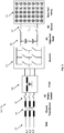
- FIG. 1 is a block diagram of a conventional photovoltaic power system 100.
- the PV power system 100 includes a solar cell array 101 that comprises a one or more solar cells (also referred to as photovoltaic cells) that convert light into DC voltage.
- the solar cells are solid state devices that convert the energy of sunlight directly into electricity by the photovoltaic effect.
- the solar cell array 101 is coupled to a DC switch 102.
- the DC switch 102 can be closed to connect the solar cell array 101 to DC capacitor bank 104, or can be opened to disconnect the solar cell array 101 from the DC capacitor bank 104.
- the solar cell array 101 can provide power to charge the DC capacitor bank 104.
- the DC capacitor bank 104 is connected to inverter 105.
- the inverter 105 converts the DC voltage output from the capacitor bank 104 into 3-phase (or in some cases 2-phase) pulsed AC voltage.
- the inverter 105 outputs pulsed AC current to a filter 106.
- the filter 106 converts the pulsed AC current output by the inverter 205 into a sinusoidal AC voltage.
- the sinusoidal AC voltage can then be output to a mains power grid 109. If an AC mains switch 107 is closed, the sinusoidal AC voltage output by the filter 106 is received by the power transformer 108.
- the power transformer 108 adapts the voltage output by the PV system 100 to the grid voltage. This configuration allows the PV system 100 to output electricity onto the mains grid 109.
- the voltage output by the photovoltaic system 100 is no higher than the grid voltage.
- Inverter 105 may have a mandatory ramp up period where the DC voltage provided by the solar cell array 101 must be gradually ramped up from an initial startup voltage to an
- FIG. 2 is a graph illustrating the characteristics of a photovoltaic cell.
- the graph is a current-voltage (I-V curve) for a typical PV cell.
- V OC represents the output voltage of the solar cell or array of solar cells where no load is connected to the PV cell or array of cells.
- Voc represents the output voltage of the solar cell array 101, because the solar cell array 101 is disconnected from the load (the grid 109).
- the value I SC represents the current produced by the PV cell or array of cells in the event that there is a short circuit.
- V max there is a maximum voltage V max where the PV cell or array of cells produces maximum power P max .
- the inverter 105 includes a DC voltage controller (not shown) that controls the DC voltage (V DC ) provided by the PV cell or array of cells to operates the PV cell or array of cells at the maximum power point.
- V DC DC voltage
- the grid voltage and the V max of the PV cell or array of cells typically do not change very quickly, so the DC-voltage controller typically does not have to dynamically respond to rapid changes in these voltages.
- the following is a typical process for powering up of a photovoltaic system, such a PV system 100.
- the PV system controller closes the DC switch 102 between the DC capacitor bank 104 and the solar cell array 101.
- the DC switch 102 has been closed, the solar array 101 is operating as a current source and begins to charge the DC capacitor bank 104 according to the specific photovoltaic cell characteristics of the solar array and the DC voltage level being generated.
- the inverter 105 closes the AC mains switch 107.
- the peak of the transformer output AC voltage is lower than Voc.
- the inverter 105 starts to generate AC voltage and the inverter 105 synchronizes its AC output voltage to grid voltage and grid frequency. AC output current of the inverter 105 during this phase of operation is approximately zero.
- the photovoltaic system is not yet generating power, and the DC voltage is V OC .
- the DC voltage controller of the photovoltaic system begins operation and reduces the DC voltage from V OC to V max . Change of the DC voltage is generally a very slow procedure.
- FIG. 2 illustrates the difference between V OC and V max . When the DC voltage is at V OC , the system is not generating power, and when the DC voltage is a V max , the system is generating maximum power.
- V DC is one of the key design parameters for photovoltaic systems, especially with respect to the components of the inverter 105 and the DC capacitor bank 104.
- the current trend for photovoltaic systems is that the V DC has been increased to higher values (e.g., in the range of 1000V).
- a lower V DC would be preferred from a design standpoint, because the inverter would not have to handle such high voltages.
- efficiency is compromised.
- the maximum DC voltage during operation of the inverter is V max , and the voltage level between V max and V DC is used only during the power up procedure.
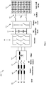
- FIG. 3 illustrates a PV system 300 that includes a power up preload 303 (also referred to herein as a power up load).
- the PV system 300 includes a solar cell array 301, a DC switch 302, a DC capacitor bank 304, an inverter 305, a filter 306, an AC mains switch 307, and a power transformer 308.
- the power transformer 308 adapts the voltage output by the PV system 300 to the grid voltage. This configuration allows the PV system 300 to output electricity onto the mains grid 309.
- the power up sequence for the PV system 300 is slightly different than that of the PV system 100, because PV system 300 includes the preload 303.
- the PV system controller closes the DC switch 302 which connects the solar cell array 301 to the power up load 303.
- the power up load 303 is disposed between the solar cell array 301 and the DC capacitor bank 304.
- the controller of the PV-inverter 305 then closes the AC mains switch 307 until the DC capacitor bank 304 is charged to V power up .
- the inverter 105 can then start generating AC voltage and the filter 306 begins synchronizing the AC output voltage and to the grid voltage and grid frequency.
- the power up load 303 is then disabled by the controller of the PV inverter 305, and the DC voltage controller of the PV system 300 being operating to reduce the DC voltage from V power up to V max in order to generate maximum power for the PV system.
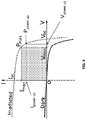
- FIG. 4 illustrates the distinction between operating at V power up where the power generated by the system equals P power up and operating at V max where the power generated by the system equals P max .
- FIG. 4 is a graph illustrating the characteristics of a photovoltaic cell that includes the power up operating point. The graph is a current-voltage (I-V curve) for a typical PV cell. V power up represents the power up voltage and I power up represent the power up current. As can be seen in FIG. 4 , the power up voltage falls between the V max and the V OC for the PV cell or array of cells.
- the inverter may be "overdesigned" to allow the inverter to operate at higher voltages such as the Voc of the solar cell array, but this approach this sacrifices efficiency of the inverter. Furthermore, adding a preload to the system as suggested in the alternative implementation illustrated in FIG. 3 can decrease the voltage levels at which the inverter can operate, but this approach adds expense and complexity to the PV system.
- Implementations of such a method may include one or more of the following features.
- the DC capacitor bank stores an electrical charge and outputs a DC current to the power inverter.
- the voltage associated with a maximum power output level of the solar cell array is less than the power up voltage for the power inverter. Closing the DC switch to allow the solar cell array to provide DC power to the DC capacitor bank to charge the DC capacitor bank when the DC voltage received from the DC capacitor bank has been stabilized at the predetermined power up voltage for the power inverter.
- the power inverter upon initiating operation, converts the DC voltage from the received from the DC capacitor bank to AC voltage that can be output onto the electrical grid.
- the DC capacitor bank stores an electrical charge and outputs a DC current to the power inverter.
- the power inverter upon initiating operation, converts the DC voltage from the received from the DC capacitor bank to AC voltage that is output to the electrical grid.
- Items and/or techniques described herein may provide one or more of the following capabilities, as well as other capabilities not mentioned.
- the inverter of the PV system can operate more efficiently and the PV system can operate with a power up load.
- Other capabilities may be provided and not every implementation according to the disclosure must provide any, let alone all, of the capabilities discussed. Further, it may be possible for an effect noted above to be achieved by means other than that noted, and a noted item/technique may not necessarily yield the noted effect.
- Techniques are described for powering up an inverter of a photovoltaic system where the inverter includes a high dynamic DC voltage controller.
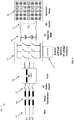
- FIG. 5 is a high level block diagram of a PV system 500.
- the inverter 505 of the PV system includes a high-dynamic DC controller 599 that has a fast current control rise time.
- the PV system 500 includes solar cell array 501.
- Solar cell array includes one or more PV cells that generate DC voltage when exposed to light using the photovoltaic effect.
- the solar cell array 501 is coupled to DC switch 102.
- the DC switch 502 can be closed to connect the solar cell array 501 to DC capacitor bank 504, or opened to disconnect the solar cell array 501 from the DC capacitor bank 504.
- the DC controller 599 can be configured to send a control signal to the DC switch 502 to open or close the switch.
- the DC controller 599 can control the operation of the DC switch 502 during a power up procedure of the inverter 505. During the power up procedure for the inverter 105, the DC controller 599 can open the DC switch 502 to disconnect the solar cell array 501 from the DC capacitor bank 504 to prevent the solar cell array 501 from charging the DC capacitor bank 504. Instead, the DC controller 599 can cause the DC capacitor bank 504 to be charged from the grid 509.
- a method for implementing a power up procedure for the inverter 505 is illustrated in FIG. 7 where the DC controller 599 charges the DC capacitor bank 504 from the grid 509 rather than from the solar cell array 501.
- the inverter 505 can be designed to operate at lower voltages which can result increased efficiency. This approach also eliminates the need to include an expensive preload to the PV system 500.
- the DC capacitor bank 504 is connected to inverter 505.
- the inverter 505 converts the DC voltage output from the capacitor bank 104 into 3-phase (or in some cases 2-phase) pulsed AC voltage.
- the inverter 105 outputs pulsed AC current to a filter 106.
- the filter 106 converts the pulsed AC current output by the inverter 205 into a sinusoidal AC voltage. The sinusoidal AC voltage can then be output to a mains power grid 109.
- the DC controller 599 can also control the operation of AC mains switch 507.
- the DC controller 599 can be configured to send a control signal to the AC mains switch 507 to close the AC mains switch 507 to allow the sinusoidal AC voltage output by the filter 506 to be received by the power transformer 508.
- the power transformer 508 adapts the voltage output by the PV system 500 to the grid voltage. This configuration allows the PV system 500 to output electricity onto the mains grid 509.
- the DC controller 599 can also send a control signal to close the AC mains switch 507 during a power up phase of the inverter 505.
- the DC controller 599 can open the DC switch 502 and close the AC mains switch 507 to disconnect the DC capacitor bank 504 from the solar cell array 504 and to allow voltage to flow from the grid 509 through the inverter 505 to the DC capacitor bank 504 to charge the DC capacitor bank. This approach allows the DC controller 599 to charge the capacitor bank 502 from the grid 509.
- the DC controller 599 can initialize the operation of the inverter 505 when the DC capacitor bank 504 has been charged to V power up . The DC controller 599 can then stabilize the operating voltage of the inverter 505 at V power up .
- the DC controller 599 can close the DC switch 502 to allow the solar cell array 501 to provide power to the DC capacitor bank 504 to charge the capacitor bank.
- the solar cell array 501 can then charge the DC capacitor bank as a current source with a constant current of I power up .
- This approach limits transient overshooting of the DC voltage (V ⁇ ) to very low levels.
- the maximum DC voltage for the operation of the inverter 505 is V power up + V ⁇ .
- the inverter 505 will not be required to operate at Voc of the solar cell array 501.
- the operating voltage of the inverter 505 can be closely controlled and kept close to V power up , which means that the inverter 505 does not need to be overdesigned to handle higher than necessary operating voltages and more efficient inverter components can be used in inverter 505.
- FIG. 6 is a block diagram of the high dynamic DC 599 for the inverter 505 of PV system 500.
- Controller 599 includes a processor 10605, memory 620, voltage inputs 635, voltmeter 630, and control interface 640.
- the memory 1020 includes a voltage control module 622 and a control signal module 1026.
- the memory 1020 can comprise one or more types of tangible, non-transitory computer-readable memory, such as random-access memory (RAM), read-only memory (ROM), flash memory, or a combination thereof.
- the modules can comprise processor-executable instructions that can be executed by processor 605.
- the processor 605 can comprise one or more microprocessors configured to access memory 620.
- the processor 605 can read data from and write data to memory 620.
- the processor 605 can also read executable program code from memory 620 and execute the program code.
- the voltage inputs 635 provide an interface through which the controller 599 can monitor voltages throughout the photovoltaic system 500.
- the voltage inputs 635 can be used to monitor the grid voltage (V grid ), the DC voltage (V DC ) provided by the solar cell array 501, and/or the voltage of the DC capacitor bank 504.
- Voltmeter 630 can be used to determine the voltage of the various inputs being monitored using the voltage inputs 635.
- the voltmeter 630 may be an external voltmeter and the controller 599 can be configured to receive a signal from the external voltmeter that monitors the the grid voltage (V grid ), the DC voltage (V DC ) provided by the solar cell array 501, and/or the voltage of the DC capacitor bank 504.
- the processor 605 can send control signals to one or more external devices via control interface 640.
- control interface 540 can be connected to AC mains switch 507 and DC capacitor bank 504 and can sent control signals to each of the switches to open and close the switches.
- the control interface can also sent a control signal to the inverter 504 to initiate a power up sequence of the inverter.
- the control interface 640 can be configured to provide wired connections, wireless connections, or a combination thereof for controlling the AC mains switch 507 and the DC capacitor bank 504, and for communicating with the inverter 505.
- the voltage control module 622 can include executable code that causes the processor 605 to perform a power up method for inverter 505 of a PV system 500.
- the voltage control module 622 can be configured to perform the stages described in the method of FIG. 7 when the inverter 505 is powered up.
- the voltage control module 622 can instruct the control signal module 626 to open and close the AC mains switch 507 and the DC switch 502 to control the flow of power through the PV system 500.
- the voltage control module 622 can also instruct the control signal module 626 to send control signals to the inverter 505.
- the voltage control module 622 can instruct the control signal module 626 to send a control signal to the inverter 505 to stop operation, to start operation, or to enter into a power up mode.
- the control signal module 626 can include executable code that can cause the processor 605 to instruct the control interface 640 to send a command to one or more external devices, such as the AC mains switch 507, the DC capacitor bank 504, and the inverter 505.
- the control signal module 626 can send a signal to the AC mains switch 507 to close the switch to provide a connection from the grid 509 to the inverter 505 or the control signal module 626 can send a signal to the AC mains switch 507 to open the switch to disconnect the grid 509 from the inverter 505.
- the control signal module 626 can send a signal to the DC switch 502 to close the switch to provide a connection from the solar cell array 501 to the DC capacitor bank 504 or the control signal module 626 can send a signal to the DC switch 502 to open the switch to disconnect the solar cell array 501 from the DC capacitor bank 504.
- FIG. 7 is a block flow diagram of a method for powering up an inverter of a photovoltaic system.
- the method for powering up a PV system illustrated in FIG. 7 can be implemented by voltage control module 622 of the controller 599 of PV system 500.
- the DC capacitor bank 504 can be charged with power from the grid before the DC switch 502 is closed to allow the solar cell array 501.
- the controller 599 of the inverter 505 can then open the DC switch 502 and the AC switch 507 (stage 705).
- the solar cell array 501 may be generating power at this point, but because the DC switch 502 is open, the solar cell array 501 cannot provide the power generated to the DC capacitor bank 504 to charge the capacitors. Also, because the AC mains switch 507 is open, PV system 500 is disconnected from the power grid 509 and is not providing power to or receiving power from the grid 509.
- the AC mains switch 507 can then be closed to connect the inverter 505 to the grid 509 (stage 710).
- Power from the grid 509 can now reach the inverter 505 that includes the high dynamic DC voltage controller.
- the inverter 505 can allow current from the grid to flow back into the DC capacitor bank 504 to charge the DC capacitor bank 504.
- the inverter converts the AC power from grid into DC power that can charge the capacitor bank 504. This approach utilizes power from the grid to charge the capacitor bank 504 rather than relying on DC current provided by the solar cell array 501.
- the inverter 505 is not operating at this point to convert DC to AC power.
- the DC voltage controller can monitor the voltage of the capacitor bank 504 (stage 715), and make a determination whether a desired voltage is reached (stage 717). If the desired voltage has not yet been reached, the controller 599 can continue to monitor the voltage of the capacitor bank.
- the capacitor bank 504 can be charged to V power up , where V power up is a desired for powering up the inverter 505. As can be seen in FIG. 4 , V power up is less than V OC but is greater than V max . Operating at V power up will place less of a strain on the inverter 505 than if the inverter 505 were operating at Voc. The inverter 505 would not need to be overdesigned to handle the higher voltage. Overdesigned systems have lower efficiency and higher complexity than systems that are not overdesigned.
- the DC voltage controller can initiate the operation of the inverter 505 (stage 720).
- the inverter 505 begins to operate and draw current from the DC capacitor bank 504 to start generating AC power and the filter 506 begins synchronizing the AC output from the inverter 505 to the voltage and frequency of the grid 509.
- the DC voltage controller then stabilizes the DC voltage of the system at power up voltage. V power up (stage 725).
- the DC voltage controller can the close the DC switch 502 (stage 730). Closing the DC switch allows DC power provided by the solar cell array 501 to charge the DC capacitor bank 504.
- the solar cell array 501 can now charging the DC capacitor bank as a current source with a constant current I power up .
- the DC voltage controller 599 can the wait for the inverter startup period to elapse (stage 735) before adjusting the DC voltage from V power up to V max to allow the PV system 500 to generate as close to maximum power from the solar cell array 501 as possible (stage 740).
- the highly dynamic DC voltage controller keeps transient overshooting of DC voltage (V ⁇ ) very low.
- V ⁇ DC voltage
- the maximum DC voltage for the inverter operation is V power up + V ⁇ .
- Additional equipment, such as a preload, can be eliminated even where the solar cell array 501 has a very high Voc.
- the inverter 505 can use higher efficiency components.
- DSP digital signal processor
- ASIC application specific integrated circuit
- FPGA field programmable gate array
- a general-purpose processor can be a microprocessor, but in the alternative, the processor can be any processor, controller, microcontroller, or state machine.
- a processor can also be implemented as a combination of computing devices, for example, a combination of a DSP and a microprocessor, multiple microprocessors, one or more microprocessors in conjunction with a DSP core, or any other such configuration.
- a software module can reside in RAM memory, flash memory, ROM memory, EPROM memory, EEPROM memory, registers, hard disk, a removable disk, a CD-ROM, or any other form of storage medium.
- An exemplary storage medium can be coupled to the processor such that the processor can read information from, and write information to, the storage medium. In the alternative, the storage medium can be integral to the processor.
- the processor and the storage medium can reside in an ASIC.
Landscapes
- Engineering & Computer Science (AREA)
- Power Engineering (AREA)
- Inverter Devices (AREA)
- Charge And Discharge Circuits For Batteries Or The Like (AREA)
- Control Of Electrical Variables (AREA)
- Photovoltaic Devices (AREA)
- Supply And Distribution Of Alternating Current (AREA)
Description
- Photovoltaic systems use solar cells to convert light into electricity. A typical photovoltaic system includes a multiple components, including photovoltaic cells, mechanical and electrical connections, mountings, and controllers for regulating and/or modifying the electrical current produced by the photovoltaic system.
EP2325984A1 discloses a method for precharging a capacitor of a direct current voltage intermediate circuit at an DC input of an inverter from an AC input via an AC grid. - The following terms are used herein to describe various components and/or operational aspects of photovoltaic systems:
- PV
- photovoltaic
- DC
- direct current
- AC
- alternate current
- ISC
- short circuit current
- VOC
- open circuit voltage
- Pmax
- maximum output power of the solar array
- Vmax
- output voltage of the solar array at maximum output power
- Imax
- output current of the solar array at maximum output power
-
FIG. 1 is a block diagram of a conventionalphotovoltaic power system 100. ThePV power system 100 includes asolar cell array 101 that comprises a one or more solar cells (also referred to as photovoltaic cells) that convert light into DC voltage. The solar cells are solid state devices that convert the energy of sunlight directly into electricity by the photovoltaic effect. Thesolar cell array 101 is coupled to aDC switch 102. TheDC switch 102 can be closed to connect thesolar cell array 101 toDC capacitor bank 104, or can be opened to disconnect thesolar cell array 101 from theDC capacitor bank 104. When theDC switch 102 is closed and thesolar cell array 101 is generating power, thesolar cell array 101 can provide power to charge theDC capacitor bank 104. - The
DC capacitor bank 104 is connected toinverter 105. Theinverter 105 converts the DC voltage output from thecapacitor bank 104 into 3-phase (or in some cases 2-phase) pulsed AC voltage. Theinverter 105 outputs pulsed AC current to afilter 106. Thefilter 106 converts the pulsed AC current output by the inverter 205 into a sinusoidal AC voltage. The sinusoidal AC voltage can then be output to amains power grid 109. If anAC mains switch 107 is closed, the sinusoidal AC voltage output by thefilter 106 is received by thepower transformer 108. Thepower transformer 108 adapts the voltage output by thePV system 100 to the grid voltage. This configuration allows thePV system 100 to output electricity onto themains grid 109. The voltage output by thephotovoltaic system 100 is no higher than the grid voltage.Inverter 105 may have a mandatory ramp up period where the DC voltage provided by thesolar cell array 101 must be gradually ramped up from an initial startup voltage to an operating voltage. -
FIG. 2 is a graph illustrating the characteristics of a photovoltaic cell. The graph is a current-voltage (I-V curve) for a typical PV cell. VOC represents the output voltage of the solar cell or array of solar cells where no load is connected to the PV cell or array of cells. In the example illustrated inFIG. 1 , when theDC switch 102 is open, Voc represents the output voltage of thesolar cell array 101, because thesolar cell array 101 is disconnected from the load (the grid 109). - The value ISC represents the current produced by the PV cell or array of cells in the event that there is a short circuit. As can be seen from the graph in
FIG. 2 , there is a maximum voltage Vmax where the PV cell or array of cells produces maximum power Pmax. In a typical photovoltaic system, such asPV power system 100, theinverter 105 includes a DC voltage controller (not shown) that controls the DC voltage (VDC) provided by the PV cell or array of cells to operates the PV cell or array of cells at the maximum power point. The grid voltage and the Vmax of the PV cell or array of cells typically do not change very quickly, so the DC-voltage controller typically does not have to dynamically respond to rapid changes in these voltages. - The following is a typical process for powering up of a photovoltaic system, such a
PV system 100. If the VDC of the solar array is higher than a predetermined threshold voltage (at least higher than the peak transformer output AC-voltage), the PV system controller closes theDC switch 102 between theDC capacitor bank 104 and thesolar cell array 101. When theDC switch 102 has been closed, thesolar array 101 is operating as a current source and begins to charge theDC capacitor bank 104 according to the specific photovoltaic cell characteristics of the solar array and the DC voltage level being generated. When theDC capacitor bank 104 has been charged to VOC, theinverter 105 closes theAC mains switch 107. The peak of the transformer output AC voltage is lower than Voc. At this point, no current is flowing between the solar array and the grid, even though all the switches are closed. Next, theinverter 105 starts to generate AC voltage and theinverter 105 synchronizes its AC output voltage to grid voltage and grid frequency. AC output current of theinverter 105 during this phase of operation is approximately zero. The photovoltaic system is not yet generating power, and the DC voltage is VOC. When theinverter 105 has begun generating AC voltage and has synchronized its output voltage with the grid voltage, the DC voltage controller of the photovoltaic system begins operation and reduces the DC voltage from VOC to Vmax. Change of the DC voltage is generally a very slow procedure.FIG. 2 illustrates the difference between VOC and Vmax. When the DC voltage is at VOC, the system is not generating power, and when the DC voltage is a Vmax, the system is generating maximum power. - The standard power up process described above has several disadvantages. For example, VDC is one of the key design parameters for photovoltaic systems, especially with respect to the components of the
inverter 105 and theDC capacitor bank 104. The current trend for photovoltaic systems is that the VDC has been increased to higher values (e.g., in the range of 1000V). A lower VDC would be preferred from a design standpoint, because the inverter would not have to handle such high voltages. In order to operate at higher voltages, efficiency is compromised. The maximum DC voltage during operation of the inverter is Vmax, and the voltage level between Vmax and VDC is used only during the power up procedure. - One technique that can be used to lower the DC voltage provided by the
solar cell array 101 is to introduce a preload into the PV system to lower the voltage provided to theinverter 105 during the ramp up period for theinverter 105.FIG. 3 illustrates aPV system 300 that includes a power up preload 303 (also referred to herein as a power up load). ThePV system 300 includes asolar cell array 301, aDC switch 302, aDC capacitor bank 304, aninverter 305, afilter 306, anAC mains switch 307, and a power transformer 308. The power transformer 308 adapts the voltage output by thePV system 300 to the grid voltage. This configuration allows thePV system 300 to output electricity onto themains grid 309. - The power up sequence for the
PV system 300 is slightly different than that of thePV system 100, becausePV system 300 includes thepreload 303. InPV system 300, the PV system controller closes theDC switch 302 which connects thesolar cell array 301 to the power upload 303. The power upload 303 is disposed between thesolar cell array 301 and theDC capacitor bank 304. The controller of the PV-inverter 305 then closes the AC mains switch 307 until theDC capacitor bank 304 is charged to Vpower up. Theinverter 105 can then start generating AC voltage and thefilter 306 begins synchronizing the AC output voltage and to the grid voltage and grid frequency. The power upload 303 is then disabled by the controller of thePV inverter 305, and the DC voltage controller of thePV system 300 being operating to reduce the DC voltage from Vpower up to Vmax in order to generate maximum power for the PV system. -
FIG. 4 illustrates the distinction between operating at Vpower up where the power generated by the system equals Ppower up and operating at Vmax where the power generated by the system equals Pmax.FIG. 4 is a graph illustrating the characteristics of a photovoltaic cell that includes the power up operating point. The graph is a current-voltage (I-V curve) for a typical PV cell. Vpower up represents the power up voltage and Ipower up represent the power up current. As can be seen inFIG. 4 , the power up voltage falls between the Vmax and the VOC for the PV cell or array of cells. - In conventional PV systems, such as those illustrated in
FIGs. 1 and3 , the inverter may be "overdesigned" to allow the inverter to operate at higher voltages such as the Voc of the solar cell array, but this approach this sacrifices efficiency of the inverter. Furthermore, adding a preload to the system as suggested in the alternative implementation illustrated inFIG. 3 can decrease the voltage levels at which the inverter can operate, but this approach adds expense and complexity to the PV system. - Aspects of the invention are disclosed in independent method claim 1.
- Implementations of such a method may include one or more of the following features. The DC capacitor bank stores an electrical charge and outputs a DC current to the power inverter. The voltage associated with a maximum power output level of the solar cell array is less than the power up voltage for the power inverter. Closing the DC switch to allow the solar cell array to provide DC power to the DC capacitor bank to charge the DC capacitor bank when the DC voltage received from the DC capacitor bank has been stabilized at the predetermined power up voltage for the power inverter. The power inverter, upon initiating operation, converts the DC voltage from the received from the DC capacitor bank to AC voltage that can be output onto the electrical grid.
- Aspects of the invention are also disclosed in independent apparatus claim 4.
- Implementation of the controller may include one or more of the following features. The DC capacitor bank stores an electrical charge and outputs a DC current to the power inverter. The power inverter, upon initiating operation, converts the DC voltage from the received from the DC capacitor bank to AC voltage that is output to the electrical grid.
- Items and/or techniques described herein may provide one or more of the following capabilities, as well as other capabilities not mentioned. The inverter of the PV system can operate more efficiently and the PV system can operate with a power up load. Other capabilities may be provided and not every implementation according to the disclosure must provide any, let alone all, of the capabilities discussed. Further, it may be possible for an effect noted above to be achieved by means other than that noted, and a noted item/technique may not necessarily yield the noted effect.
-
-
FIG. 1 is a high level block diagram of a conventional photovoltaic system. -
FIG. 2 is an I-V curve for a solar cell that illustrates the maximum power point for the solar cell. -
FIG. 3 is a high level block diagram of another conventional PV system that includes a preload. -
FIG. 4 is an I-V curve for a solar cell that illustrates the characteristics of a photovoltaic cell and a power up loading operating point. -
FIG. 5 is a high level block diagram of a PV system that includes a DC controller for the PV inverter of the PV system. -
FIG. 6 is a block diagram of a DC controller for a PV inverter. -
FIG. 7 is a block flow diagram of a method for powering up a photovoltaic system. - Techniques are described for powering up an inverter of a photovoltaic system where the inverter includes a high dynamic DC voltage controller.
-
FIG. 5 is a high level block diagram of aPV system 500. Theinverter 505 of the PV system includes a high-dynamic DC controller 599 that has a fast current control rise time. ThePV system 500 includessolar cell array 501. Solar cell array includes one or more PV cells that generate DC voltage when exposed to light using the photovoltaic effect. Thesolar cell array 501 is coupled toDC switch 102. TheDC switch 502 can be closed to connect thesolar cell array 501 toDC capacitor bank 504, or opened to disconnect thesolar cell array 501 from theDC capacitor bank 504. TheDC controller 599 can be configured to send a control signal to theDC switch 502 to open or close the switch. - The
DC controller 599 can control the operation of theDC switch 502 during a power up procedure of theinverter 505. During the power up procedure for theinverter 105, theDC controller 599 can open theDC switch 502 to disconnect thesolar cell array 501 from theDC capacitor bank 504 to prevent thesolar cell array 501 from charging theDC capacitor bank 504. Instead, theDC controller 599 can cause theDC capacitor bank 504 to be charged from thegrid 509. A method for implementing a power up procedure for theinverter 505 is illustrated inFIG. 7 where theDC controller 599 charges theDC capacitor bank 504 from thegrid 509 rather than from thesolar cell array 501. By charging theDC capacitor bank 504 from thegrid 509 rather than thesolar cell array 504 during the startup period for theinverter 505, theinverter 505 can be designed to operate at lower voltages which can result increased efficiency. This approach also eliminates the need to include an expensive preload to thePV system 500. - The
DC capacitor bank 504 is connected toinverter 505. Theinverter 505 converts the DC voltage output from thecapacitor bank 104 into 3-phase (or in some cases 2-phase) pulsed AC voltage. Theinverter 105 outputs pulsed AC current to afilter 106. Thefilter 106 converts the pulsed AC current output by the inverter 205 into a sinusoidal AC voltage. The sinusoidal AC voltage can then be output to amains power grid 109. - The
DC controller 599 can also control the operation of AC mains switch 507. TheDC controller 599 can be configured to send a control signal to the AC mains switch 507 to close the AC mains switch 507 to allow the sinusoidal AC voltage output by thefilter 506 to be received by thepower transformer 508. Thepower transformer 508 adapts the voltage output by thePV system 500 to the grid voltage. This configuration allows thePV system 500 to output electricity onto themains grid 509. TheDC controller 599 can also send a control signal to close the AC mains switch 507 during a power up phase of theinverter 505. During the power up phase of theinverter 505, theDC controller 599 can open theDC switch 502 and close the AC mains switch 507 to disconnect theDC capacitor bank 504 from thesolar cell array 504 and to allow voltage to flow from thegrid 509 through theinverter 505 to theDC capacitor bank 504 to charge the DC capacitor bank. This approach allows theDC controller 599 to charge thecapacitor bank 502 from thegrid 509. TheDC controller 599 can initialize the operation of theinverter 505 when theDC capacitor bank 504 has been charged to Vpower up. TheDC controller 599 can then stabilize the operating voltage of theinverter 505 at Vpower up. - The
DC controller 599 can close theDC switch 502 to allow thesolar cell array 501 to provide power to theDC capacitor bank 504 to charge the capacitor bank. Thesolar cell array 501 can then charge the DC capacitor bank as a current source with a constant current of Ipower up. This approach limits transient overshooting of the DC voltage (VΔ) to very low levels. As a result, the maximum DC voltage for the operation of theinverter 505 is Vpower up + VΔ. Theinverter 505 will not be required to operate at Voc of thesolar cell array 501. Accordingly, even in systems where thesolar cell array 501 has a very high Voc, the operating voltage of theinverter 505 can be closely controlled and kept close to Vpower up, which means that theinverter 505 does not need to be overdesigned to handle higher than necessary operating voltages and more efficient inverter components can be used ininverter 505. -
FIG. 6 is a block diagram of the highdynamic DC 599 for theinverter 505 ofPV system 500.Controller 599 includes a processor 10605,memory 620, voltage inputs 635, voltmeter 630, andcontrol interface 640. The memory 1020 includes avoltage control module 622 and a control signal module 1026. The memory 1020 can comprise one or more types of tangible, non-transitory computer-readable memory, such as random-access memory (RAM), read-only memory (ROM), flash memory, or a combination thereof. The modules can comprise processor-executable instructions that can be executed byprocessor 605. - The
processor 605 can comprise one or more microprocessors configured to accessmemory 620. Theprocessor 605 can read data from and write data tomemory 620. Theprocessor 605 can also read executable program code frommemory 620 and execute the program code. - The voltage inputs 635 provide an interface through which the
controller 599 can monitor voltages throughout thephotovoltaic system 500. For example, the voltage inputs 635 can be used to monitor the grid voltage (Vgrid), the DC voltage (VDC) provided by thesolar cell array 501, and/or the voltage of theDC capacitor bank 504. Voltmeter 630 can be used to determine the voltage of the various inputs being monitored using the voltage inputs 635. The voltmeter 630 may be an external voltmeter and thecontroller 599 can be configured to receive a signal from the external voltmeter that monitors the the grid voltage (Vgrid), the DC voltage (VDC) provided by thesolar cell array 501, and/or the voltage of theDC capacitor bank 504. - The
processor 605 can send control signals to one or more external devices viacontrol interface 640. For example, control interface 540 can be connected to AC mains switch 507 andDC capacitor bank 504 and can sent control signals to each of the switches to open and close the switches. The control interface can also sent a control signal to theinverter 504 to initiate a power up sequence of the inverter. Thecontrol interface 640 can be configured to provide wired connections, wireless connections, or a combination thereof for controlling the AC mains switch 507 and theDC capacitor bank 504, and for communicating with theinverter 505. - The
voltage control module 622 can include executable code that causes theprocessor 605 to perform a power up method forinverter 505 of aPV system 500. Thevoltage control module 622 can be configured to perform the stages described in the method ofFIG. 7 when theinverter 505 is powered up. Thevoltage control module 622 can instruct thecontrol signal module 626 to open and close the AC mains switch 507 and theDC switch 502 to control the flow of power through thePV system 500. Thevoltage control module 622 can also instruct thecontrol signal module 626 to send control signals to theinverter 505. For example, thevoltage control module 622 can instruct thecontrol signal module 626 to send a control signal to theinverter 505 to stop operation, to start operation, or to enter into a power up mode. - The
control signal module 626 can include executable code that can cause theprocessor 605 to instruct thecontrol interface 640 to send a command to one or more external devices, such as the AC mains switch 507, theDC capacitor bank 504, and theinverter 505. For example, thecontrol signal module 626 can send a signal to the AC mains switch 507 to close the switch to provide a connection from thegrid 509 to theinverter 505 or thecontrol signal module 626 can send a signal to the AC mains switch 507 to open the switch to disconnect thegrid 509 from theinverter 505. Thecontrol signal module 626 can send a signal to theDC switch 502 to close the switch to provide a connection from thesolar cell array 501 to theDC capacitor bank 504 or thecontrol signal module 626 can send a signal to theDC switch 502 to open the switch to disconnect thesolar cell array 501 from theDC capacitor bank 504. -
FIG. 7 is a block flow diagram of a method for powering up an inverter of a photovoltaic system. The method for powering up a PV system illustrated inFIG. 7 can be implemented byvoltage control module 622 of thecontroller 599 ofPV system 500. In the method illustrated inFIG. 7 , theDC capacitor bank 504 can be charged with power from the grid before theDC switch 502 is closed to allow thesolar cell array 501. - The
controller 599 of theinverter 505 can then open theDC switch 502 and the AC switch 507 (stage 705). Thesolar cell array 501 may be generating power at this point, but because theDC switch 502 is open, thesolar cell array 501 cannot provide the power generated to theDC capacitor bank 504 to charge the capacitors. Also, because the AC mains switch 507 is open,PV system 500 is disconnected from thepower grid 509 and is not providing power to or receiving power from thegrid 509. - The AC mains switch 507 can then be closed to connect the
inverter 505 to the grid 509 (stage 710). Power from thegrid 509 can now reach theinverter 505 that includes the high dynamic DC voltage controller. Theinverter 505 can allow current from the grid to flow back into theDC capacitor bank 504 to charge theDC capacitor bank 504. The inverter converts the AC power from grid into DC power that can charge thecapacitor bank 504. This approach utilizes power from the grid to charge thecapacitor bank 504 rather than relying on DC current provided by thesolar cell array 501. Theinverter 505 is not operating at this point to convert DC to AC power. - The DC voltage controller can monitor the voltage of the capacitor bank 504 (stage 715), and make a determination whether a desired voltage is reached (stage 717). If the desired voltage has not yet been reached, the
controller 599 can continue to monitor the voltage of the capacitor bank. In one example, thecapacitor bank 504 can be charged to Vpower up, where Vpower up is a desired for powering up theinverter 505. As can be seen inFIG. 4 , Vpower up is less than VOC but is greater than Vmax. Operating at Vpower up will place less of a strain on theinverter 505 than if theinverter 505 were operating at Voc. Theinverter 505 would not need to be overdesigned to handle the higher voltage. Overdesigned systems have lower efficiency and higher complexity than systems that are not overdesigned. - With the DC capacitor bank at the desired charge level, the DC voltage controller can initiate the operation of the inverter 505 (stage 720). The
inverter 505 begins to operate and draw current from theDC capacitor bank 504 to start generating AC power and thefilter 506 begins synchronizing the AC output from theinverter 505 to the voltage and frequency of thegrid 509. - The DC voltage controller then stabilizes the DC voltage of the system at power up voltage. Vpower up (stage 725). The DC voltage controller can the close the DC switch 502 (stage 730). Closing the DC switch allows DC power provided by the
solar cell array 501 to charge theDC capacitor bank 504. Thesolar cell array 501 can now charging the DC capacitor bank as a current source with a constant current Ipower up. - The
DC voltage controller 599 can the wait for the inverter startup period to elapse (stage 735) before adjusting the DC voltage from Vpower up to Vmax to allow thePV system 500 to generate as close to maximum power from thesolar cell array 501 as possible (stage 740). - The highly dynamic DC voltage controller keeps transient overshooting of DC voltage (VΔ) very low. As a result, the maximum DC voltage for the inverter operation is Vpower up + VΔ. Additional equipment, such as a preload, can be eliminated even where the
solar cell array 501 has a very high Voc. Furthermore, because the operating voltages of theinverter 505 have been reduced, theinverter 505 can use higher efficiency components. - The various illustrative logical blocks, modules, and algorithm stages described may be implemented as electronic hardware, computer software, or combinations of both. To clearly illustrate this interchangeability of hardware and software, various illustrative components, blocks, modules, and stages have been described above generally in terms of their functionality. Whether such functionality is implemented as hardware or software depends upon the design constraints imposed on the overall system. The described functionality can be implemented in varying ways. In addition, the grouping of functions within a module, block or stage is for ease of description. Specific functions can be moved from one module or block without departing from the disclosure.
- The various illustrative logical blocks and modules described can be implemented or performed with a general purpose processor, a digital signal processor (DSP), application specific integrated circuit (ASIC), a field programmable gate array (FPGA) or other programmable logic device, discrete gate or transistor logic, discrete hardware components, or any combination thereof designed to perform the functions described herein. A general-purpose processor can be a microprocessor, but in the alternative, the processor can be any processor, controller, microcontroller, or state machine. A processor can also be implemented as a combination of computing devices, for example, a combination of a DSP and a microprocessor, multiple microprocessors, one or more microprocessors in conjunction with a DSP core, or any other such configuration.
- The operations of a method or algorithm described may be embodied directly in hardware, in a software module executed by a processor, or in a combination of the two. A software module can reside in RAM memory, flash memory, ROM memory, EPROM memory, EEPROM memory, registers, hard disk, a removable disk, a CD-ROM, or any other form of storage medium. An exemplary storage medium can be coupled to the processor such that the processor can read information from, and write information to, the storage medium. In the alternative, the storage medium can be integral to the processor. The processor and the storage medium can reside in an ASIC.
- Various changes and modifications could be made to the descriptions provided above without departing from the scope of the disclosure or the appended claims. For example, although elements may be described or claimed in the singular, the plural may be included. Additionally, all or portions of aspects and/or embodiments may be utilized with other aspects and/or embodiments.
Claims (6)
- A method for initializing the power inverter (105,305,505) of a photovoltaic system (100,300,500) comprising a solar cell array (101,301,501), comprising:opening an alternating current AC mains switch (107,307,507) and a direct current DC switch (102,302,502), wherein opening the AC mains switch (107,307,507) disconnects the power (105,305,505) from an electrical grid (109,30,509), and wherein opening the DC switch (102,302,502) disconnects a DC capacitor bank (104,304,504) associated with a power inverter (105,305,505) from the solar cell array (101,301,501) to prevent the solar cell array (101,301,501) from charging the DC capacitor bank (104,304,504);closing the AC mains switch (107,307,507) to allow power to flow from the electrical grid (109,30,509) to the DC capacitor bank (104,304,504) connected to the power inverter (105,305,505) to charge the DC capacitor bank (104,304,504);monitoring the DC capacitor bank (104,304,504) until a desired power-up voltage (Vpower up) for the DC capacitor bank (104,304,504) is reached;initiating the operation of the power inverter (105,305,505) such that the power inverter (105,305,505) begins to receive DC voltage from the DC capacitor bank (104,304,504) responsive to the DC capacitor bank (104,304,504) being charged up to the power up voltage (Vpower up) of the power inverter (105,305,505);stabilizing the DC voltage received from the DC capacitor bank (104,304,504) at the power up voltage (Vpower up) for the power inverter (105,305,505), the power up voltage (Vpower up) of the power inverter (105,305,505) being greater than a maximum output voltage (Vmax) of the solar cell array and less than an open circuit voltage (Voc) for the solar cell array (101,301,501) without a load connected to the solar cell array (101,301,501);closing the DC switch (102,302,502) to allow the solar cell array (101,301,501) to provide DC power to the DC capacitor bank (104,304,504) to charge the DC capacitor bank (104,304,504) when the DC voltage received from the DC capacitor bank (104,304,504) has been stabilized at the power-up voltage (Vpower up) such that the solar cell array (101,301,501) provides a constant power up current to the DC capacitor bank (104,304,504) to minimize transient overshooting of the power-up voltage (Vpower up);waiting for an inverter initialization period to elapse; andadjusting DC voltage received by power inverter (105,305,505) to the maximum output voltage (Vmax).
- The method of claim 1 wherein the DC capacitor bank (104,304,504) stores an electrical charge and outputs a DC current to the power inverter (105,305,505).
- The method of claim 1 wherein the power inverter (105,305,505), upon initiating operation, converts the DC voltage received from the DC capacitor bank (104,304,504) to AC voltage that is output to the electrical grid (109,309,509).
- A controller (599) for a photovoltaic system (500) the photovoltaic system (500) comprising a solar cell array (501), a direct current DC capacitor bank (504), an alternating current AC switch (507), and a DC switch (502), the controller (599) comprising:a tangible, non-transitory computer-readable memory (620);a plurality of modules (622,626) comprising processor executable code stored in the memory (620);a processor (605) connected to the memory (620) and configured to access the plurality of modules (622,626) stored in the memory (620); anda control interface (640) configured to send control signals to the AC switch, (507) the DC switch (502), and the power inverter (505);wherein the plurality of modules (622,626) stored in the memory (620) includes:a voltage control module (622) configured to cause the processor (605) to perform a method for initializing the power inverter (505) of the photovoltaic system (500) comprising:opening an alternating current mains switch (507) and a direct current switch (502), wherein opening the AC mains switch (507) disconnects the power inverter (505) from an electrical grid (509), and wherein opening the DC switch (502) disconnects the power inverter (505) from the solar cell array (501) to prevent the solar cell array (501) from charging the DC capacitor bank (504),closing the AC mains switch (507)to allow power to flow from the electrical grid (509) to a DC capacitor bank (504) connected to the power inverter (505) to charge the DC capacitor bank (504),monitoring the DC capacitor bank (504) until a desired power-up voltage (Vpower up) for the DC capacitor bank (504) is reached,initiating the operation of the power inverter (505) such that the power inverter (505) begins to receive DC voltage from the DC capacitor bank (504) responsive to the DC capacitor bank (504) being charged up to the power up voltage (Vpower up) of the power inverter (505),stabilizing the DC voltage received from the DC capacitor bank (504) at the power up voltage for the power inverter (505), the power up voltage of the power inverter (505) being greater than a maximum output power of the solar cell array (501) and less than an open circuit voltage for the solar cell array (501) without a load connected to the solar cell array (501),close the DC switch (502) to allow the solar cell array (501) to provide DC power to the DC capacitor bank (504) to charge the DC capacitor bank (504) when the DC voltage received from the DC capacitor bank (504) has been stabilized at the predetermined power up voltage for the power inverter (505) such that the solar cell array (501) provides a constant power up current to the DC capacitor bank (504) to minimize transient overshooting of the power-up voltage (Vpower up);waiting for an inverter initialization period to elapse, andadjusting DC voltage received by power inverter (505) to the maximum output voltage (Vmax);a control signal module (599) configured to cause the processor (605) to send control signals to the AC switch (507) the DC switch (502), and the power inverter (505) over the control interface (640).
- The controller of claim 4 wherein the DC capacitor bank (504) stores an electrical charge and outputs a DC current to the power inverter (505).
- The controller of claim 4 wherein the power inverter (505), upon initiating operation, converts the DC voltage from the DC capacitor bank (504) to AC voltage that is output to the electrical grid (509)
Applications Claiming Priority (3)
| Application Number | Priority Date | Filing Date | Title |
|---|---|---|---|
| US201161493045P | 2011-06-03 | 2011-06-03 | |
| US13/159,396 US9343906B2 (en) | 2011-06-03 | 2011-06-13 | High dynamic DC-voltage controller for photovoltaic inverter |
| PCT/US2012/039595 WO2012166605A2 (en) | 2011-06-03 | 2012-05-25 | High dynamic dc-voltage controller for photovoltaic inverter |
Publications (3)
| Publication Number | Publication Date |
|---|---|
| EP2715928A2 EP2715928A2 (en) | 2014-04-09 |
| EP2715928A4 EP2715928A4 (en) | 2014-12-03 |
| EP2715928B1 true EP2715928B1 (en) | 2017-12-27 |
Family
ID=47260218
Family Applications (1)
| Application Number | Title | Priority Date | Filing Date |
|---|---|---|---|
| EP12792382.9A Revoked EP2715928B1 (en) | 2011-06-03 | 2012-05-25 | High dynamic dc-voltage controller for photovoltaic inverter |
Country Status (5)
| Country | Link |
|---|---|
| US (1) | US9343906B2 (en) |
| EP (1) | EP2715928B1 (en) |
| CN (1) | CN103733464B (en) |
| ES (1) | ES2664222T3 (en) |
| WO (1) | WO2012166605A2 (en) |
Cited By (1)
| Publication number | Priority date | Publication date | Assignee | Title |
|---|---|---|---|---|
| EP4513705A4 (en) * | 2022-07-29 | 2025-07-30 | Huawei Digital Power Tech Co Ltd | Photovoltaic power supply system and control method therefor |
Families Citing this family (12)
| Publication number | Priority date | Publication date | Assignee | Title |
|---|---|---|---|---|
| KR101871020B1 (en) * | 2014-03-20 | 2018-07-19 | 엘에스산전 주식회사 | system for charging battery of energy storage system using PCS |
| US20150288183A1 (en) | 2014-04-06 | 2015-10-08 | CleanSpark Technologies LLC | Establishing communication and power sharing links between components of a distributed energy system |
| CN104167799B (en) * | 2014-08-29 | 2017-10-17 | 阳光电源股份有限公司 | A kind of charge-discharge system, method and photovoltaic generating system |
| EP3051686B1 (en) | 2015-01-27 | 2017-11-01 | ABB Schweiz AG | Method for testing electric system and electric system |
| US9812867B2 (en) | 2015-06-12 | 2017-11-07 | Black Night Enterprises, Inc. | Capacitor enhanced multi-element photovoltaic cell |
| JP6097864B1 (en) * | 2016-05-27 | 2017-03-15 | 田淵電機株式会社 | Power interconnection device for grid interconnection having self-sustaining operation function and start control method thereof |
| KR20180024169A (en) * | 2016-08-29 | 2018-03-08 | 엘에스산전 주식회사 | Photovoltaic inverter |
| JP6913871B2 (en) * | 2017-12-27 | 2021-08-04 | パナソニックIpマネジメント株式会社 | Control command system and power converter |
| US10516365B1 (en) | 2018-06-20 | 2019-12-24 | Schneider Electric Solar Inverters Usa, Inc. | DC voltage control in renewable energy based multilevel power converter |
| CN114586278B (en) * | 2019-08-29 | 2026-04-03 | 康泰(澳洲)有限公司 | Solar power monitoring and optimization equipment, systems and methods |
| EP4195450A4 (en) * | 2020-09-30 | 2023-10-04 | Huawei Digital Power Technologies Co., Ltd. | CHARGING BLOCK AND CHARGING SYSTEM |
| CN118232502B (en) * | 2024-05-24 | 2024-08-30 | 深圳市格伏恩新能源科技有限公司 | Photovoltaic charging system and photovoltaic charging control method |
Citations (5)
| Publication number | Priority date | Publication date | Assignee | Title |
|---|---|---|---|---|
| EP1463188A2 (en) | 2003-03-22 | 2004-09-29 | SMA Regelsysteme GmbH | Circuit arrangement, accessory module and photovoltaic system |
| US20090167097A1 (en) | 2007-12-31 | 2009-07-02 | Eric Seymour | Photovoltaic inverter interface device, system, and method |
| WO2010040613A1 (en) | 2008-10-06 | 2010-04-15 | Siemens Aktiengesellschaft | Protective circuit for an intermediate circuit of an inverter, particularly a solar inverter, against overvoltages |
| US20100275966A1 (en) | 2009-11-25 | 2010-11-04 | American Superconductor Corporation | Reducing photovoltaic array voltage during inverter re-enablement |
| EP2325984A1 (en) | 2009-11-24 | 2011-05-25 | SMA Solar Technology AG | Start up of a photovoltiac field with high open circuit voltage |
Family Cites Families (10)
| Publication number | Priority date | Publication date | Assignee | Title |
|---|---|---|---|---|
| JP3096378B2 (en) | 1993-09-01 | 2000-10-10 | シャープ株式会社 | Power supply system start / stop control device |
| US6128204A (en) | 1998-08-26 | 2000-10-03 | Northrop Grumman Corporation | Line power unit for micropower generation |
| US7269036B2 (en) | 2003-05-12 | 2007-09-11 | Siemens Vdo Automotive Corporation | Method and apparatus for adjusting wakeup time in electrical power converter systems and transformer isolation |
| US8013472B2 (en) | 2006-12-06 | 2011-09-06 | Solaredge, Ltd. | Method for distributed power harvesting using DC power sources |
| WO2009014522A1 (en) * | 2007-07-26 | 2009-01-29 | Utc Power Corporation | Power system having ac and dc power sources |
| US8018748B2 (en) | 2007-11-14 | 2011-09-13 | General Electric Company | Method and system to convert direct current (DC) to alternating current (AC) using a photovoltaic inverter |
| WO2009134756A1 (en) | 2008-04-29 | 2009-11-05 | Cirrus Logic, Inc. | Cascaded switching power converter for coupling a photovoltaic energy source to power mains |
| US7768155B2 (en) | 2008-10-10 | 2010-08-03 | Enphase Energy, Inc. | Method and apparatus for improved burst mode during power conversion |
| EP2282388A1 (en) | 2009-08-06 | 2011-02-09 | SMA Solar Technology AG | Device for feeding in electrical energy of a number of strings of photovoltaic modules in an electricity network |
| US8599586B2 (en) * | 2010-08-28 | 2013-12-03 | General Electric Company | Power inverter system and method of starting same at high DC voltage |
-
2011
- 2011-06-13 US US13/159,396 patent/US9343906B2/en not_active Expired - Fee Related
-
2012
- 2012-05-25 CN CN201280038485.2A patent/CN103733464B/en not_active Expired - Fee Related
- 2012-05-25 WO PCT/US2012/039595 patent/WO2012166605A2/en not_active Ceased
- 2012-05-25 EP EP12792382.9A patent/EP2715928B1/en not_active Revoked
- 2012-05-25 ES ES12792382.9T patent/ES2664222T3/en active Active
Patent Citations (7)
| Publication number | Priority date | Publication date | Assignee | Title |
|---|---|---|---|---|
| EP1463188A2 (en) | 2003-03-22 | 2004-09-29 | SMA Regelsysteme GmbH | Circuit arrangement, accessory module and photovoltaic system |
| US20090167097A1 (en) | 2007-12-31 | 2009-07-02 | Eric Seymour | Photovoltaic inverter interface device, system, and method |
| WO2010040613A1 (en) | 2008-10-06 | 2010-04-15 | Siemens Aktiengesellschaft | Protective circuit for an intermediate circuit of an inverter, particularly a solar inverter, against overvoltages |
| EP2325984A1 (en) | 2009-11-24 | 2011-05-25 | SMA Solar Technology AG | Start up of a photovoltiac field with high open circuit voltage |
| WO2011064232A2 (en) | 2009-11-24 | 2011-06-03 | Sma Solar Technology Ag | Connecting a photovoltaic array at a high open circuit voltage |
| EP2504909B1 (en) | 2009-11-24 | 2014-04-02 | SMA Solar Technology AG | Start-up of a photovoltaic array with high open circuit voltage |
| US20100275966A1 (en) | 2009-11-25 | 2010-11-04 | American Superconductor Corporation | Reducing photovoltaic array voltage during inverter re-enablement |
Non-Patent Citations (2)
| Title |
|---|
| "Initialisieren", DUDEN ONLINE WÖRTERBUCH, 2018, XP055522811, Retrieved from the Internet <URL:https://www.duden.de/suchen/dudenonline/initialisieren> |
| DIN: "Sicherheit von Wechselrichtern zur Anwendung in photovoltaischenEnergiesystemen - Teil 1: Allgemeine Anforderungen", DIN EN 62109-1 (VDE 0126-14-1), April 2011 (2011-04-01), XP055522813 |
Cited By (1)
| Publication number | Priority date | Publication date | Assignee | Title |
|---|---|---|---|---|
| EP4513705A4 (en) * | 2022-07-29 | 2025-07-30 | Huawei Digital Power Tech Co Ltd | Photovoltaic power supply system and control method therefor |
Also Published As
| Publication number | Publication date |
|---|---|
| ES2664222T3 (en) | 2018-04-18 |
| CN103733464A (en) | 2014-04-16 |
| WO2012166605A3 (en) | 2013-02-07 |
| EP2715928A2 (en) | 2014-04-09 |
| US9343906B2 (en) | 2016-05-17 |
| WO2012166605A2 (en) | 2012-12-06 |
| CN103733464B (en) | 2017-05-10 |
| US20120310438A1 (en) | 2012-12-06 |
| EP2715928A4 (en) | 2014-12-03 |
| WO2012166605A4 (en) | 2013-04-25 |
Similar Documents
| Publication | Publication Date | Title |
|---|---|---|
| EP2715928B1 (en) | High dynamic dc-voltage controller for photovoltaic inverter | |
| US10305285B2 (en) | Photovoltaic voltage regulation | |
| KR102610010B1 (en) | Method and system for extracting excess power | |
| EP2991183B1 (en) | Charging and discharging system and method, and photovoltaic power generation system | |
| EP2991184B1 (en) | Method for startup control of photovoltaic inverter, system thereof, and photovoltaic power generation system | |
| KR101830666B1 (en) | Power conversion apparatus | |
| CN105144534A (en) | Inverter synchronization | |
| US11128142B2 (en) | Photovoltaic power generation system and method for controlling the same | |
| CN104253530A (en) | Photovoltaic inverter, control method of photovoltaic inverter and photovoltaic power generation system with photovoltaic inverter | |
| CN104685755A (en) | Power control system and solar power generation system | |
| KR101871020B1 (en) | system for charging battery of energy storage system using PCS | |
| EP2991209B1 (en) | Method for controlling shutdown of photovoltaic inverters, system thereof, and photovoltaic power generation system | |
| CN107017767B (en) | A kind of method and device of solar battery array open circuit overvoltage protection, inverter | |
| EP3419142A1 (en) | Power storage system and power storage method | |
| JP2015204746A (en) | Method of supplying energy from photovoltaic power generation module of photovoltaic power generation system and inverter designed to implement the method | |
| US20110156633A1 (en) | Solar power storage system and charge method of same | |
| JP6351200B2 (en) | Power supply system | |
| JP4877092B2 (en) | Distributed power system | |
| CN104158219B (en) | A kind of photovoltaic DC-to-AC converter shutdown control method, system and photovoltaic generating system | |
| KR20160073652A (en) | Method and apparatus for controlling a solar array power | |
| US20180191010A1 (en) | Protection circuit for a fuel cell and method of use | |
| NZ749353A (en) | Method and apparatus for bidirectional storage and renewable power converter |
Legal Events
| Date | Code | Title | Description |
|---|---|---|---|
| PUAI | Public reference made under article 153(3) epc to a published international application that has entered the european phase |
Free format text: ORIGINAL CODE: 0009012 |
|
| 17P | Request for examination filed |
Effective date: 20131209 |
|
| AK | Designated contracting states |
Kind code of ref document: A2 Designated state(s): AL AT BE BG CH CY CZ DE DK EE ES FI FR GB GR HR HU IE IS IT LI LT LU LV MC MK MT NL NO PL PT RO RS SE SI SK SM TR |
|
| RIN1 | Information on inventor provided before grant (corrected) |
Inventor name: KAISER, KARL |
|
| DAX | Request for extension of the european patent (deleted) | ||
| A4 | Supplementary search report drawn up and despatched |
Effective date: 20141104 |
|
| RIC1 | Information provided on ipc code assigned before grant |
Ipc: H02J 3/38 20060101ALI20141029BHEP Ipc: H02M 7/42 20060101AFI20141029BHEP |
|
| 17Q | First examination report despatched |
Effective date: 20161004 |
|
| STAA | Information on the status of an ep patent application or granted ep patent |
Free format text: STATUS: EXAMINATION IS IN PROGRESS |
|
| GRAP | Despatch of communication of intention to grant a patent |
Free format text: ORIGINAL CODE: EPIDOSNIGR1 |
|
| STAA | Information on the status of an ep patent application or granted ep patent |
Free format text: STATUS: GRANT OF PATENT IS INTENDED |
|
| INTG | Intention to grant announced |
Effective date: 20170613 |
|
| GRAS | Grant fee paid |
Free format text: ORIGINAL CODE: EPIDOSNIGR3 |
|
| GRAJ | Information related to disapproval of communication of intention to grant by the applicant or resumption of examination proceedings by the epo deleted |
Free format text: ORIGINAL CODE: EPIDOSDIGR1 |
|
| GRAL | Information related to payment of fee for publishing/printing deleted |
Free format text: ORIGINAL CODE: EPIDOSDIGR3 |
|
| STAA | Information on the status of an ep patent application or granted ep patent |
Free format text: STATUS: EXAMINATION IS IN PROGRESS |
|
| INTC | Intention to grant announced (deleted) | ||
| GRAR | Information related to intention to grant a patent recorded |
Free format text: ORIGINAL CODE: EPIDOSNIGR71 |
|
| STAA | Information on the status of an ep patent application or granted ep patent |
Free format text: STATUS: GRANT OF PATENT IS INTENDED |
|
| GRAA | (expected) grant |
Free format text: ORIGINAL CODE: 0009210 |
|
| STAA | Information on the status of an ep patent application or granted ep patent |
Free format text: STATUS: THE PATENT HAS BEEN GRANTED |
|
| INTG | Intention to grant announced |
Effective date: 20171116 |
|
| AK | Designated contracting states |
Kind code of ref document: B1 Designated state(s): AL AT BE BG CH CY CZ DE DK EE ES FI FR GB GR HR HU IE IS IT LI LT LU LV MC MK MT NL NO PL PT RO RS SE SI SK SM TR |
|
| REG | Reference to a national code |
Ref country code: GB Ref legal event code: FG4D |
|
| REG | Reference to a national code |
Ref country code: CH Ref legal event code: EP |
|
| REG | Reference to a national code |
Ref country code: AT Ref legal event code: REF Ref document number: 959098 Country of ref document: AT Kind code of ref document: T Effective date: 20180115 |
|
| REG | Reference to a national code |
Ref country code: IE Ref legal event code: FG4D |
|
| REG | Reference to a national code |
Ref country code: DE Ref legal event code: R096 Ref document number: 602012041416 Country of ref document: DE |
|
| REG | Reference to a national code |
Ref country code: ES Ref legal event code: FG2A Ref document number: 2664222 Country of ref document: ES Kind code of ref document: T3 Effective date: 20180418 |
|
| PG25 | Lapsed in a contracting state [announced via postgrant information from national office to epo] |
Ref country code: LT Free format text: LAPSE BECAUSE OF FAILURE TO SUBMIT A TRANSLATION OF THE DESCRIPTION OR TO PAY THE FEE WITHIN THE PRESCRIBED TIME-LIMIT Effective date: 20171227 Ref country code: NO Free format text: LAPSE BECAUSE OF FAILURE TO SUBMIT A TRANSLATION OF THE DESCRIPTION OR TO PAY THE FEE WITHIN THE PRESCRIBED TIME-LIMIT Effective date: 20180327 Ref country code: FI Free format text: LAPSE BECAUSE OF FAILURE TO SUBMIT A TRANSLATION OF THE DESCRIPTION OR TO PAY THE FEE WITHIN THE PRESCRIBED TIME-LIMIT Effective date: 20171227 |
|
| REG | Reference to a national code |
Ref country code: NL Ref legal event code: MP Effective date: 20171227 |
|
| REG | Reference to a national code |
Ref country code: LT Ref legal event code: MG4D |
|
| REG | Reference to a national code |
Ref country code: AT Ref legal event code: MK05 Ref document number: 959098 Country of ref document: AT Kind code of ref document: T Effective date: 20171227 |
|
| REG | Reference to a national code |
Ref country code: FR Ref legal event code: PLFP Year of fee payment: 7 |
|
| PG25 | Lapsed in a contracting state [announced via postgrant information from national office to epo] |
Ref country code: HR Free format text: LAPSE BECAUSE OF FAILURE TO SUBMIT A TRANSLATION OF THE DESCRIPTION OR TO PAY THE FEE WITHIN THE PRESCRIBED TIME-LIMIT Effective date: 20171227 Ref country code: LV Free format text: LAPSE BECAUSE OF FAILURE TO SUBMIT A TRANSLATION OF THE DESCRIPTION OR TO PAY THE FEE WITHIN THE PRESCRIBED TIME-LIMIT Effective date: 20171227 Ref country code: RS Free format text: LAPSE BECAUSE OF FAILURE TO SUBMIT A TRANSLATION OF THE DESCRIPTION OR TO PAY THE FEE WITHIN THE PRESCRIBED TIME-LIMIT Effective date: 20171227 Ref country code: BG Free format text: LAPSE BECAUSE OF FAILURE TO SUBMIT A TRANSLATION OF THE DESCRIPTION OR TO PAY THE FEE WITHIN THE PRESCRIBED TIME-LIMIT Effective date: 20180327 Ref country code: GR Free format text: LAPSE BECAUSE OF FAILURE TO SUBMIT A TRANSLATION OF THE DESCRIPTION OR TO PAY THE FEE WITHIN THE PRESCRIBED TIME-LIMIT Effective date: 20180328 |
|
| PG25 | Lapsed in a contracting state [announced via postgrant information from national office to epo] |
Ref country code: NL Free format text: LAPSE BECAUSE OF FAILURE TO SUBMIT A TRANSLATION OF THE DESCRIPTION OR TO PAY THE FEE WITHIN THE PRESCRIBED TIME-LIMIT Effective date: 20171227 |
|
| PG25 | Lapsed in a contracting state [announced via postgrant information from national office to epo] |
Ref country code: CY Free format text: LAPSE BECAUSE OF FAILURE TO SUBMIT A TRANSLATION OF THE DESCRIPTION OR TO PAY THE FEE WITHIN THE PRESCRIBED TIME-LIMIT Effective date: 20171227 Ref country code: EE Free format text: LAPSE BECAUSE OF FAILURE TO SUBMIT A TRANSLATION OF THE DESCRIPTION OR TO PAY THE FEE WITHIN THE PRESCRIBED TIME-LIMIT Effective date: 20171227 Ref country code: CZ Free format text: LAPSE BECAUSE OF FAILURE TO SUBMIT A TRANSLATION OF THE DESCRIPTION OR TO PAY THE FEE WITHIN THE PRESCRIBED TIME-LIMIT Effective date: 20171227 Ref country code: SK Free format text: LAPSE BECAUSE OF FAILURE TO SUBMIT A TRANSLATION OF THE DESCRIPTION OR TO PAY THE FEE WITHIN THE PRESCRIBED TIME-LIMIT Effective date: 20171227 |
|
| PGFP | Annual fee paid to national office [announced via postgrant information from national office to epo] |
Ref country code: DE Payment date: 20180529 Year of fee payment: 7 Ref country code: ES Payment date: 20180601 Year of fee payment: 7 |
|
| PG25 | Lapsed in a contracting state [announced via postgrant information from national office to epo] |
Ref country code: IT Free format text: LAPSE BECAUSE OF FAILURE TO SUBMIT A TRANSLATION OF THE DESCRIPTION OR TO PAY THE FEE WITHIN THE PRESCRIBED TIME-LIMIT Effective date: 20171227 Ref country code: AT Free format text: LAPSE BECAUSE OF FAILURE TO SUBMIT A TRANSLATION OF THE DESCRIPTION OR TO PAY THE FEE WITHIN THE PRESCRIBED TIME-LIMIT Effective date: 20171227 Ref country code: SM Free format text: LAPSE BECAUSE OF FAILURE TO SUBMIT A TRANSLATION OF THE DESCRIPTION OR TO PAY THE FEE WITHIN THE PRESCRIBED TIME-LIMIT Effective date: 20171227 Ref country code: IS Free format text: LAPSE BECAUSE OF FAILURE TO SUBMIT A TRANSLATION OF THE DESCRIPTION OR TO PAY THE FEE WITHIN THE PRESCRIBED TIME-LIMIT Effective date: 20180427 Ref country code: RO Free format text: LAPSE BECAUSE OF FAILURE TO SUBMIT A TRANSLATION OF THE DESCRIPTION OR TO PAY THE FEE WITHIN THE PRESCRIBED TIME-LIMIT Effective date: 20171227 Ref country code: PL Free format text: LAPSE BECAUSE OF FAILURE TO SUBMIT A TRANSLATION OF THE DESCRIPTION OR TO PAY THE FEE WITHIN THE PRESCRIBED TIME-LIMIT Effective date: 20171227 |
|
| PGFP | Annual fee paid to national office [announced via postgrant information from national office to epo] |
Ref country code: FR Payment date: 20180525 Year of fee payment: 7 |
|
| REG | Reference to a national code |
Ref country code: DE Ref legal event code: R026 Ref document number: 602012041416 Country of ref document: DE |
|
| PLBI | Opposition filed |
Free format text: ORIGINAL CODE: 0009260 |
|
| PLAX | Notice of opposition and request to file observation + time limit sent |
Free format text: ORIGINAL CODE: EPIDOSNOBS2 |
|
| 26 | Opposition filed |
Opponent name: SMA SOLAR TECHNOLOGY AG Effective date: 20180926 |
|
| PGFP | Annual fee paid to national office [announced via postgrant information from national office to epo] |
Ref country code: GB Payment date: 20180529 Year of fee payment: 7 |
|
| PG25 | Lapsed in a contracting state [announced via postgrant information from national office to epo] |
Ref country code: DK Free format text: LAPSE BECAUSE OF FAILURE TO SUBMIT A TRANSLATION OF THE DESCRIPTION OR TO PAY THE FEE WITHIN THE PRESCRIBED TIME-LIMIT Effective date: 20171227 |
|
| REG | Reference to a national code |
Ref country code: CH Ref legal event code: PL |
|
| REG | Reference to a national code |
Ref country code: BE Ref legal event code: MM Effective date: 20180531 |
|
| PG25 | Lapsed in a contracting state [announced via postgrant information from national office to epo] |
Ref country code: MC Free format text: LAPSE BECAUSE OF FAILURE TO SUBMIT A TRANSLATION OF THE DESCRIPTION OR TO PAY THE FEE WITHIN THE PRESCRIBED TIME-LIMIT Effective date: 20171227 |
|
| REG | Reference to a national code |
Ref country code: IE Ref legal event code: MM4A |
|
| PG25 | Lapsed in a contracting state [announced via postgrant information from national office to epo] |
Ref country code: SI Free format text: LAPSE BECAUSE OF FAILURE TO SUBMIT A TRANSLATION OF THE DESCRIPTION OR TO PAY THE FEE WITHIN THE PRESCRIBED TIME-LIMIT Effective date: 20171227 Ref country code: CH Free format text: LAPSE BECAUSE OF NON-PAYMENT OF DUE FEES Effective date: 20180531 Ref country code: LI Free format text: LAPSE BECAUSE OF NON-PAYMENT OF DUE FEES Effective date: 20180531 |
|
| PLBB | Reply of patent proprietor to notice(s) of opposition received |
Free format text: ORIGINAL CODE: EPIDOSNOBS3 |
|
| PG25 | Lapsed in a contracting state [announced via postgrant information from national office to epo] |
Ref country code: LU Free format text: LAPSE BECAUSE OF NON-PAYMENT OF DUE FEES Effective date: 20180525 |
|
| PG25 | Lapsed in a contracting state [announced via postgrant information from national office to epo] |
Ref country code: IE Free format text: LAPSE BECAUSE OF NON-PAYMENT OF DUE FEES Effective date: 20180525 |
|
| PG25 | Lapsed in a contracting state [announced via postgrant information from national office to epo] |
Ref country code: BE Free format text: LAPSE BECAUSE OF NON-PAYMENT OF DUE FEES Effective date: 20180531 |
|
| RDAF | Communication despatched that patent is revoked |
Free format text: ORIGINAL CODE: EPIDOSNREV1 |
|
| REG | Reference to a national code |
Ref country code: DE Ref legal event code: R064 Ref document number: 602012041416 Country of ref document: DE Ref country code: DE Ref legal event code: R103 Ref document number: 602012041416 Country of ref document: DE |
|
| REG | Reference to a national code |
Ref country code: DE Ref legal event code: R119 Ref document number: 602012041416 Country of ref document: DE |
|
| GBPC | Gb: european patent ceased through non-payment of renewal fee |
Effective date: 20190525 |
|
| PG25 | Lapsed in a contracting state [announced via postgrant information from national office to epo] |
Ref country code: MT Free format text: LAPSE BECAUSE OF NON-PAYMENT OF DUE FEES Effective date: 20180525 |
|
| RDAG | Patent revoked |
Free format text: ORIGINAL CODE: 0009271 |
|
| STAA | Information on the status of an ep patent application or granted ep patent |
Free format text: STATUS: PATENT REVOKED |
|
| 27W | Patent revoked |
Effective date: 20191129 |
|
| REG | Reference to a national code |
Ref country code: FI Ref legal event code: MGE |
|
| PG25 | Lapsed in a contracting state [announced via postgrant information from national office to epo] |
Ref country code: GB Free format text: LAPSE BECAUSE OF NON-PAYMENT OF DUE FEES Effective date: 20190525 Ref country code: PT Free format text: LAPSE BECAUSE OF FAILURE TO SUBMIT A TRANSLATION OF THE DESCRIPTION OR TO PAY THE FEE WITHIN THE PRESCRIBED TIME-LIMIT Effective date: 20171227 |
|
| PG25 | Lapsed in a contracting state [announced via postgrant information from national office to epo] |
Ref country code: FR Free format text: LAPSE BECAUSE OF NON-PAYMENT OF DUE FEES Effective date: 20190531 Ref country code: MK Free format text: LAPSE BECAUSE OF NON-PAYMENT OF DUE FEES Effective date: 20171227 |
|
| PG25 | Lapsed in a contracting state [announced via postgrant information from national office to epo] |
Ref country code: AL Free format text: LAPSE BECAUSE OF FAILURE TO SUBMIT A TRANSLATION OF THE DESCRIPTION OR TO PAY THE FEE WITHIN THE PRESCRIBED TIME-LIMIT Effective date: 20171227 |
|
| PG25 | Lapsed in a contracting state [announced via postgrant information from national office to epo] |
Ref country code: SE Free format text: LAPSE BECAUSE OF NON-PAYMENT OF DUE FEES Effective date: 20171227 |
|
| PG25 | Lapsed in a contracting state [announced via postgrant information from national office to epo] |
Ref country code: TR Free format text: LAPSE BECAUSE OF FAILURE TO SUBMIT A TRANSLATION OF THE DESCRIPTION OR TO PAY THE FEE WITHIN THE PRESCRIBED TIME-LIMIT Effective date: 20171227 |
|
| PG25 | Lapsed in a contracting state [announced via postgrant information from national office to epo] |
Ref country code: ES Free format text: LAPSE BECAUSE OF NON-PAYMENT OF DUE FEES Effective date: 20190526 |
|
| PG25 | Lapsed in a contracting state [announced via postgrant information from national office to epo] |
Ref country code: ES Free format text: LAPSE BECAUSE OF NON-PAYMENT OF DUE FEES Effective date: 20190526 |