EP2712078A1 - Cellule d'unité logique magnétique (MLU) et amplificateur possédant un signal magnétique linéaire - Google Patents
Cellule d'unité logique magnétique (MLU) et amplificateur possédant un signal magnétique linéaire Download PDFInfo
- Publication number
- EP2712078A1 EP2712078A1 EP12290315.6A EP12290315A EP2712078A1 EP 2712078 A1 EP2712078 A1 EP 2712078A1 EP 12290315 A EP12290315 A EP 12290315A EP 2712078 A1 EP2712078 A1 EP 2712078A1
- Authority
- EP
- European Patent Office
- Prior art keywords
- magnetic
- magnetization
- field
- mlu
- layer
- Prior art date
- Legal status (The legal status is an assumption and is not a legal conclusion. Google has not performed a legal analysis and makes no representation as to the accuracy of the status listed.)
- Granted
Links
- 230000005291 magnetic effect Effects 0.000 title claims abstract description 124
- 230000005415 magnetization Effects 0.000 claims abstract description 79
- 230000004888 barrier function Effects 0.000 claims abstract description 4
- 238000003860 storage Methods 0.000 claims description 27
- 230000004044 response Effects 0.000 claims description 5
- 230000002441 reversible effect Effects 0.000 claims description 4
- 230000005294 ferromagnetic effect Effects 0.000 description 10
- 230000008878 coupling Effects 0.000 description 7
- 238000010168 coupling process Methods 0.000 description 7
- 238000005859 coupling reaction Methods 0.000 description 7
- 230000005290 antiferromagnetic effect Effects 0.000 description 5
- 238000000034 method Methods 0.000 description 3
- 230000008569 process Effects 0.000 description 3
- 239000000758 substrate Substances 0.000 description 3
- KJTLSVCANCCWHF-UHFFFAOYSA-N Ruthenium Chemical compound [Ru] KJTLSVCANCCWHF-UHFFFAOYSA-N 0.000 description 2
- 238000006073 displacement reaction Methods 0.000 description 2
- 230000006870 function Effects 0.000 description 2
- 238000010438 heat treatment Methods 0.000 description 2
- 230000006911 nucleation Effects 0.000 description 2
- 238000010899 nucleation Methods 0.000 description 2
- 229910052707 ruthenium Inorganic materials 0.000 description 2
- VYZAMTAEIAYCRO-UHFFFAOYSA-N Chromium Chemical compound [Cr] VYZAMTAEIAYCRO-UHFFFAOYSA-N 0.000 description 1
- 229910003321 CoFe Inorganic materials 0.000 description 1
- 229910019236 CoFeB Inorganic materials 0.000 description 1
- RYGMFSIKBFXOCR-UHFFFAOYSA-N Copper Chemical compound [Cu] RYGMFSIKBFXOCR-UHFFFAOYSA-N 0.000 description 1
- 229910001030 Iron–nickel alloy Inorganic materials 0.000 description 1
- BQCADISMDOOEFD-UHFFFAOYSA-N Silver Chemical compound [Ag] BQCADISMDOOEFD-UHFFFAOYSA-N 0.000 description 1
- 239000000956 alloy Substances 0.000 description 1
- 229910045601 alloy Inorganic materials 0.000 description 1
- WYTGDNHDOZPMIW-RCBQFDQVSA-N alstonine Natural products C1=CC2=C3C=CC=CC3=NC2=C2N1C[C@H]1[C@H](C)OC=C(C(=O)OC)[C@H]1C2 WYTGDNHDOZPMIW-RCBQFDQVSA-N 0.000 description 1
- 230000003321 amplification Effects 0.000 description 1
- 238000000137 annealing Methods 0.000 description 1
- 230000000903 blocking effect Effects 0.000 description 1
- 229910052804 chromium Inorganic materials 0.000 description 1
- 239000011651 chromium Substances 0.000 description 1
- 238000005253 cladding Methods 0.000 description 1
- 229910052802 copper Inorganic materials 0.000 description 1
- 239000010949 copper Substances 0.000 description 1
- 230000001419 dependent effect Effects 0.000 description 1
- 230000000694 effects Effects 0.000 description 1
- 238000005516 engineering process Methods 0.000 description 1
- 229910052741 iridium Inorganic materials 0.000 description 1
- GKOZUEZYRPOHIO-UHFFFAOYSA-N iridium atom Chemical compound [Ir] GKOZUEZYRPOHIO-UHFFFAOYSA-N 0.000 description 1
- 238000004519 manufacturing process Methods 0.000 description 1
- 230000000873 masking effect Effects 0.000 description 1
- 239000000463 material Substances 0.000 description 1
- 238000003199 nucleic acid amplification method Methods 0.000 description 1
- 229910052702 rhenium Inorganic materials 0.000 description 1
- WUAPFZMCVAUBPE-UHFFFAOYSA-N rhenium atom Chemical compound [Re] WUAPFZMCVAUBPE-UHFFFAOYSA-N 0.000 description 1
- 229910052703 rhodium Inorganic materials 0.000 description 1
- 239000010948 rhodium Substances 0.000 description 1
- MHOVAHRLVXNVSD-UHFFFAOYSA-N rhodium atom Chemical compound [Rh] MHOVAHRLVXNVSD-UHFFFAOYSA-N 0.000 description 1
- 229910052709 silver Inorganic materials 0.000 description 1
- 239000004332 silver Substances 0.000 description 1
- 229910052727 yttrium Inorganic materials 0.000 description 1
- VWQVUPCCIRVNHF-UHFFFAOYSA-N yttrium atom Chemical compound [Y] VWQVUPCCIRVNHF-UHFFFAOYSA-N 0.000 description 1
Images


Classifications
-
- H—ELECTRICITY
- H10—SEMICONDUCTOR DEVICES; ELECTRIC SOLID-STATE DEVICES NOT OTHERWISE PROVIDED FOR
- H10N—ELECTRIC SOLID-STATE DEVICES NOT OTHERWISE PROVIDED FOR
- H10N50/00—Galvanomagnetic devices
- H10N50/80—Constructional details
-
- H—ELECTRICITY
- H03—ELECTRONIC CIRCUITRY
- H03F—AMPLIFIERS
- H03F15/00—Amplifiers using galvano-magnetic effects not involving mechanical movement, e.g. using Hall effect
-
- G—PHYSICS
- G11—INFORMATION STORAGE
- G11C—STATIC STORES
- G11C11/00—Digital stores characterised by the use of particular electric or magnetic storage elements; Storage elements therefor
- G11C11/02—Digital stores characterised by the use of particular electric or magnetic storage elements; Storage elements therefor using magnetic elements
- G11C11/16—Digital stores characterised by the use of particular electric or magnetic storage elements; Storage elements therefor using magnetic elements using elements in which the storage effect is based on magnetic spin effect
- G11C11/165—Auxiliary circuits
- G11C11/1675—Writing or programming circuits or methods
-
- H—ELECTRICITY
- H03—ELECTRONIC CIRCUITRY
- H03K—PULSE TECHNIQUE
- H03K19/00—Logic circuits, i.e. having at least two inputs acting on one output; Inverting circuits
- H03K19/02—Logic circuits, i.e. having at least two inputs acting on one output; Inverting circuits using specified components
- H03K19/18—Logic circuits, i.e. having at least two inputs acting on one output; Inverting circuits using specified components using galvano-magnetic devices, e.g. Hall-effect devices
Definitions
- the present invention concerns a Magnetic logic unit (MLU) cell and amplifier having a linear magnetic signal.
- MLU Magnetic logic unit
- a conventional MRAM cell comprises a magnetic tunnel junction comprising a ferromagnetic reference layer and a ferromagnetic storage layer.
- TAS MRAM thermally-assisted-switching
- the storage layer is blocked by an antiferromagnetic layer such as to achieve superior stability in normal operating temperatures.
- the temperature of the cell is momentarily locally raised above a blocking temperature of the antiferromagnetic layer, through resistive heating of the magnetic tunnel junction, allowing the magnetoresistance of the TAS-MRAM cell to be varied.
- the information stored in TAS-MRAM memory cells is thus not affected by external fields and noise.
- Self-referenced MRAM cells can be based on TAS MRAM cells.
- Self-referenced MRAM cells typically have the reference layer that is not pinned by an antiferromagnetic layer but is free to be varied. Such unpinned reference layer is often called "sense layer".
- sense layer When a current is applied in a field line adjacent to the MRAM cell, a magnetic field is generated such as to vary the sense layer magnetization during a read operation.
- a two-phase read operation utilizes the natural tendency of an un-driven field line's effect on a selected memory cell to create a momentary reference value that is compared to the cell's value when the field is driven. The stored information is thus read as this field is applied.
- MRAM magnetic random access memory
- a magnetic logic unit (MLU) cell is built on the self-referenced TAS MRAM technology. During logic operations the field lines are acting as controlling gates modulating the resistivity of the magnetic tunnel junction.
- the MLU cell behaves as a three-terminal device capable of performing native logical functions. The currents circulating in the field line can be modulated in direction, and intensity.
- a MLU amplifier can be provided by electrically coupling an array comprising several (possibly tens of thousands) of MLU cells together.
- the gain of the resulting amplifier is largely increased device while the coupling capacitance remains very small.
- the magnetoresistance of the magnetic tunnel junction is modulated by the direction of a field current flowing through a field line which is set by an input bit to be matched.
- a high or low magnetoresistance at the output indicates whether the input bit matches the stored bit or not, respectively.
- N the total number of magnetic tunnel junctions in the array
- P mtj the power delivered by a single magnetic tunnel junction.
- the MLU amplifier is an active device that can be built without any CMOS substrate. Consequently, a low cost five mask process on a bare substrate can be appropriate to manufacture such MLU amplifier. Only two extra masking processes on a standard CMOS process will enable System On a Chip capability that integrates MLU amplifier solutions.
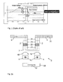
- Fig. 1 shows an output voltage and an output current generated by the MLU amplifier upon passing an input current in a current line electrically connecting in series the plurality of MLU cells.
- the input current need to be set at the cutoff level where the output impedance is in the middle of the potential excursion to deliver the highest gain.
- the AC signal at the input stage will create large resistance variations in the output stage, creating a large output signal.
- class A For linear amplification, class A, this current needs to be adjusted to the particular point where slope of the IV curve is the highest.
- class C the input set up will be where the DC power is at its minimum (all magnetic tunnel junctions having their storage and sense magnetization parallel).
- the output of the MLU cell and of the MLU amplifier can be determined by a hysteresis loop reporting the applied magnetic field against the magnetization of the MLU cell(s).
- the presence of a large hysteresis curve will prevent the MLU amplifier to operate on a class C mode, and will require at least a full 1mA input peak current swing to operate class C.
- the present disclosure concerns a magnetic logic unit (MLU) cell comprising: a first magnetic tunnel junction and a second magnetic tunnel junction, each magnetic tunnel junction comprising a first magnetic layer having a first magnetization, a secondmagnetic layer having a second magnetization that is reversible at a high temperature threshold and pinned at a low temperature threshold, and a tunnel barrier layer between the first and second magnetic layer; a strap electrically connecting one end of the first magnetic tunnel junction in series with one end of the second magnetic tunnel junction; and a field line for passing a field current such as to generate an external magnetic field adapted to switch the first magnetization; the first magnetic layer being arranged such that the magnetic tunnel junction magnetization varies linearly with the generated external magnetic field.
- MLU magnetic logic unit
- the present disclosure also concerns an MLU amplifier comprising a plurality of the MLU cell, wherein the MLU cells are electrically connected in series via a current line.
- the disclosed MLU amplifier has large gains and extended cut off frequencies.
- the MLU amplifier maximizes the linearity and / or the TMR.
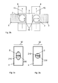
- Fig.2 shows a cross section view (a) and a top view (b) of an MLU cell 1.
- the MLU cell 1 comprises a first and a second magnetic tunnel junction 2, each of the two magnetic tunnel junctions 2 being electrically connected in series at one end via a strap 7. The other end of each of the magnetic tunnel junctions 2 is electrically connected to a current line 3.
- the current line 3 can be used to pass a heating current during a write operation or a read current during a read operation.
- the MLU cell 1 further comprises a field line 4 arranged for passing a field current 41 such as to generate an external magnetic field 42.
- the field line 4 is represented as two parallel field line portions 4' located at the end of the magnetic tunnel junctions 2 connecting the strap 7.
- the field line 4 (or each of the field line portions 4') can preferably comprise a cladding.
- Each magnetic tunnel junction 2 comprises a first magnetic layer (or sense layer) 21 having a first magnetization (or sense magnetization) 210, a second magnetic layer (or storage layer) 23 having a second magnetization 230 (or storage magnetization), and a tunnel barrier layer 22 separating the sense magnetic layer 21 from the storage magnetic layer 23.
- the first magnetization 210 can be reversible and the second magnetization 230 can be adjustable when the magnetic tunnel junction 2 is at a high temperature threshold and pinned at a low temperature threshold.
- the magnetic tunnel junction 2 can further comprise an antiferromagnetic layer 24 arranged for pinning the second magnetization at a low temperature threshold and freeing it at a high temperature threshold.
- the storage and sense magnetizations are aligned antiparallel.
- the sense magnetizations can be aligned in a parallel fashion by passing a field current in the filed lines 4.
- the sense magnetization 210 comprises an anisotropy that is substantially perpendicular to the storage magnetization 230 and parallel to the field line 4. In such configuration, passing the field current 41 in the field line 4 will generate the external magnetic field 42 with an orientation being substantially perpendicular with the direction of the sense magnetization 210.
- the corresponding magnetization curve represented in Fig. 4 does not show any opening of the hysteresis loop, but rather a linear variation of the magnetic tunnel junction magnetization M (corresponding to the variation in the sense magnetization 210) with the magnitude H of the applied external magnetic field 42 until the applied external magnetic field 42 reaches a saturation magnetic field H SAT .
- the anisotropy is obtained by the sense layer 21 comprising an anisotropic shape with the long dimension of the anisotropic shape being substantially perpendicular to the storage magnetization 230 and substantially parallel to the field line 4.
- the anisotropic shape is obtained by the sense layer 21 having elliptically shape with the long axis being substantially perpendicular to the storage magnetization 230 and substantially parallel to the field line 4.
- the anisotropy is obtained by the sense layer 21 comprising a uniaxial magnetocrystalline anisotropy being oriented substantially perpendicular to the storage magnetization 230 and substantially parallel to the field line 4.
- the MLU cell 1 further comprises a weak transverse biasing field 52 (see Fig. 2a ) adapted to orient the sense magnetization 210 substantially perpendicular to the storage magnetization 230 and substantially parallel to the field line 4.
- the transverse biasing field 52 can be generated by a permanent magnet 50 located, for example, at one end of the magnetic tunnel junctions 2 on the side of the field line 4 or on the side opposed to the field line 4.
- the storage layer 23 is preferably stabilized by using an annealing step while applying a uniform external field or by writing using the field line 4.
- the sense layer 21 comprises a vortex micromagnetic configuration of the sense magnetization 210.
- the storage layer 23 can comprise a synthetic antiferromagnet or "SAF" storage layer.
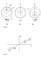
- a plan view of the sense layer 21 is shown, wherein the sense magnetization 210 represented by the arrows comprises a magnetization vortex 8.
- the magnetization vortex 8 can be obtained by having the shape of the sense layer 21 with an aspect ratio that is approximately 1 (and preferably less than 1.3) and with a predetermined thickness.
- Fig. 6a represents the sense magnetization vortex 8 in the absence of the external magnetic field 42, with a vortex center 9 being substantially at a center of the sense layer cross-section.
- Fig. 6b shows the vortex center 9 being moved upwards upon applying the external magnetic field 42 in a first direction represented toward the left in Fig. 6b.
- Fig. 6c shows the vortex center 9 being moved downwards upon applying the external magnetic field 42 in a second direction, opposed to the first direction.
- the displacement of the vortex center 9 upwards results in a net magnetic moment H ⁇ 0 in the sense layer 21, whereas the displacement of the vortex center 9 downwards upwards ( Fig. 6c ) results in a net magnetic moment H > 0 in the sense layer 21.
- the hysteresis response to the applied external magnetic field 42 comprises a reversible linear portion corresponding to the movement of the vortex center 9 perpendicular to the applied external magnetic field 42.
- the values and the slope of the linear part of hysteresis loop are strongly dependent on the size of the sense layer 21.
- the sense layer 21 comprises a SAF sense layer.
- the sense layer 21 comprises a first sense ferromagnetic layer 211 having a first sense magnetization 2111, and a second sense ferromagnetic layer 212 having a second sense magnetization 2121.
- the magnetization of the two sense ferromagnetic layers 211, 212 is coupled in an anti-parallel direction due to the presence of a anti-parallel coupling layer 213.
- the two sense ferromagnetic layers 211, 212 can be made of a CoFe, CoFeB or NiFe alloy and have a thickness typically comprised between about 1.5 nm and about 4 nm.
- the storage anti-parallel coupling layer 232 can be realized using a non-magnetic separating layer with material selected from a group consisting of ruthenium, chromium, rhenium, iridium, rhodium, silver, copper and yttrium.
- the anti-parallel coupling layer 213 is made of ruthenium and has a thickness typically comprised between about 0.6 nm and 2nm, preferably between 0.6nm and about 0.9 nm or between about 1.6nm and about 2nm.
- Fig. 9 represents a magnetization curve of the SAF sense layer 21 for the case where the external magnetic field 42 is applied substantially perpendicular to the anisotropy axis of the sense layer 21.
- Symbol H denote the magnitude of the magnetic field 42 and symbol M denotes the magnetization values of the first and second sense magnetization 2111, 2121.
- the SAF sense layer 21 is configured such that the magnetization response curve shows a hysteresis loop delimited by spin-flop value H SF of the magnetic field 42.
- the first sense magnetization 2111 is no more antiparallel with the second sense magnetization 2121 but forms a predetermined angle ⁇ with the second sense magnetization 2121.
- the magnetic field is further increased, the first sense magnetization 2111 becomes oriented substantially parallel to the second sense magnetization 2121.
- the magnitude of the magnetic field 42 required to orients the first sense magnetization 2111 substantially parallel to the second sense magnetization 2121 is referred to as the saturation magnetic field H SAT .
- the magnetization curve shows a hysteresis loop delimited by spin-flop value B SF of the magnetic field 42.
- the first storage magnetization 233 is no more antiparallel with the second storage magnetization but forms a predetermined angle ⁇ . with the second storage magnetization (see Figs. 4a and 4b).
- the first storage magnetization 233 becomes oriented substantially parallel to the second storage magnetization 234.
- the magnitude of the magnetic field 42 required to orients the first storage magnetization 233 substantially parallel to the second storage magnetization 234 is referred to as the saturation magnetic field B SAT .
- a linear response on the hysteresis loop can thus be obtained for a magnitude H of the external magnetic field 42 comprised between the spin-flop value H SF and the saturation magnetic field H SAT .
- Increasing TMR of the magnetic tunnel junction 2 can also increase the difference between the two states, and increase linearity of the response.
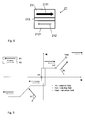
- Fig. 10 shows an MLU amplifier comprising a plurality of MLU cells 1 disclosed herein, the MLU cells 1 being electrically connected in series via the current line 3.
- the magnetic tunnel junctions of the plurality of MLU cells are all connected in series with each other via the current line 3 and the strap 7. Such configuration allows for increasing the output signal and the current gain.
- the plurality of MLU cells is electrically connected in series in a way such as to avoid contact to the substrate.
- the field lines 4 of each MLU cell are electrically connected in series such as to form a continuous field line 4 in the array.
- the field line 4 can take the shape of a serpentine.
Landscapes
- Engineering & Computer Science (AREA)
- Computer Hardware Design (AREA)
- Power Engineering (AREA)
- Physics & Mathematics (AREA)
- Computing Systems (AREA)
- General Engineering & Computer Science (AREA)
- Mathematical Physics (AREA)
- Hall/Mr Elements (AREA)
- Mram Or Spin Memory Techniques (AREA)
Priority Applications (3)
| Application Number | Priority Date | Filing Date | Title |
|---|---|---|---|
| EP12290315.6A EP2712078B1 (fr) | 2012-09-25 | 2012-09-25 | Cellule d'unité logique magnétique (MLU) et amplificateur possédant un signal magnétique linéaire |
| PCT/EP2013/068867 WO2014048758A1 (fr) | 2012-09-25 | 2013-09-12 | Cellule d'unité logique magnétique (mlu) et amplificateur ayant un signal magnétique linéaire |
| US14/431,125 US9583695B2 (en) | 2012-09-25 | 2013-09-12 | Magnetic logic unit (MLU) cell and amplifier having a linear magnetic signal |
Applications Claiming Priority (1)
| Application Number | Priority Date | Filing Date | Title |
|---|---|---|---|
| EP12290315.6A EP2712078B1 (fr) | 2012-09-25 | 2012-09-25 | Cellule d'unité logique magnétique (MLU) et amplificateur possédant un signal magnétique linéaire |
Publications (2)
| Publication Number | Publication Date |
|---|---|
| EP2712078A1 true EP2712078A1 (fr) | 2014-03-26 |
| EP2712078B1 EP2712078B1 (fr) | 2015-06-03 |
Family
ID=47520811
Family Applications (1)
| Application Number | Title | Priority Date | Filing Date |
|---|---|---|---|
| EP12290315.6A Active EP2712078B1 (fr) | 2012-09-25 | 2012-09-25 | Cellule d'unité logique magnétique (MLU) et amplificateur possédant un signal magnétique linéaire |
Country Status (3)
| Country | Link |
|---|---|
| US (1) | US9583695B2 (fr) |
| EP (1) | EP2712078B1 (fr) |
| WO (1) | WO2014048758A1 (fr) |
Cited By (1)
| Publication number | Priority date | Publication date | Assignee | Title |
|---|---|---|---|---|
| EP3101654A1 (fr) * | 2015-06-05 | 2016-12-07 | Crocus Technology | Dispositif magnétique configuré pour réaliser une fonction de circuit additionneur analogique et procédé de fonctionnement d'un tel dispositif magnétique |
Families Citing this family (4)
| Publication number | Priority date | Publication date | Assignee | Title |
|---|---|---|---|---|
| US10989769B2 (en) | 2013-12-27 | 2021-04-27 | Infineon Technologies Ag | Magneto-resistive structured device having spontaneously generated in-plane closed flux magnetization pattern |
| EP3023803B1 (fr) * | 2014-11-19 | 2020-03-18 | Crocus Technology S.A. | Cellule MLU pour détecter un champ magnétique externe et dispositif de capteur magnétique comprenant une cellule MLU |
| US9866182B2 (en) | 2015-05-15 | 2018-01-09 | Crocus Technology Inc. | MRAM-based pre-distortion linearization and amplification circuits |
| DE102016112008A1 (de) | 2016-06-30 | 2018-01-04 | Infineon Technologies Ag | Magnetsensorbauelement und magneterfassungsverfahren |
Citations (5)
| Publication number | Priority date | Publication date | Assignee | Title |
|---|---|---|---|---|
| US6356147B1 (en) * | 2000-12-19 | 2002-03-12 | International Business Machines Corporation | Wideband dual amplifier circuits |
| US20050216244A1 (en) * | 2004-03-23 | 2005-09-29 | Nahas Joseph J | Magnetoresistive random access memory simulation |
| WO2009074411A1 (fr) * | 2007-12-13 | 2009-06-18 | Crocus Technology | Mémoire magnétique à procédure d'écriture assistée thermiquement |
| US20100193890A1 (en) * | 2007-08-03 | 2010-08-05 | Tetsuhiro Suzuki | Magnetic domain wall random access memory |
| US20120201073A1 (en) * | 2011-02-08 | 2012-08-09 | Neal Berger | Memory Devices with Series-Interconnected Magnetic Random Access Memory Cells |
Family Cites Families (3)
| Publication number | Priority date | Publication date | Assignee | Title |
|---|---|---|---|---|
| US7619431B2 (en) * | 2003-12-23 | 2009-11-17 | Nxp B.V. | High sensitivity magnetic built-in current sensor |
| TWI449040B (zh) * | 2006-10-06 | 2014-08-11 | Crocus Technology Sa | 用於提供內容可定址的磁阻式隨機存取記憶體單元之系統及方法 |
| EP2270812B1 (fr) * | 2009-07-02 | 2017-01-18 | CROCUS Technology | Mémoire associative ternaire à base de mémoire à accès aléatoire magnétique final |
-
2012
- 2012-09-25 EP EP12290315.6A patent/EP2712078B1/fr active Active
-
2013
- 2013-09-12 WO PCT/EP2013/068867 patent/WO2014048758A1/fr active Application Filing
- 2013-09-12 US US14/431,125 patent/US9583695B2/en active Active
Patent Citations (5)
| Publication number | Priority date | Publication date | Assignee | Title |
|---|---|---|---|---|
| US6356147B1 (en) * | 2000-12-19 | 2002-03-12 | International Business Machines Corporation | Wideband dual amplifier circuits |
| US20050216244A1 (en) * | 2004-03-23 | 2005-09-29 | Nahas Joseph J | Magnetoresistive random access memory simulation |
| US20100193890A1 (en) * | 2007-08-03 | 2010-08-05 | Tetsuhiro Suzuki | Magnetic domain wall random access memory |
| WO2009074411A1 (fr) * | 2007-12-13 | 2009-06-18 | Crocus Technology | Mémoire magnétique à procédure d'écriture assistée thermiquement |
| US20120201073A1 (en) * | 2011-02-08 | 2012-08-09 | Neal Berger | Memory Devices with Series-Interconnected Magnetic Random Access Memory Cells |
Cited By (3)
| Publication number | Priority date | Publication date | Assignee | Title |
|---|---|---|---|---|
| EP3101654A1 (fr) * | 2015-06-05 | 2016-12-07 | Crocus Technology | Dispositif magnétique configuré pour réaliser une fonction de circuit additionneur analogique et procédé de fonctionnement d'un tel dispositif magnétique |
| WO2016193908A1 (fr) | 2015-06-05 | 2016-12-08 | Crocus Technology Sa | Dispositif magnétique configuré afin d'exécuter une fonction de sommateur analogique, et procédé de fonctionnement d'un tel dispositif magnétique |
| US10157652B2 (en) | 2015-06-05 | 2018-12-18 | Crocus Technology Sa | Magnetic device configured to perform an analog adder circuit function and method for operating such magnetic device |
Also Published As
| Publication number | Publication date |
|---|---|
| WO2014048758A1 (fr) | 2014-04-03 |
| US9583695B2 (en) | 2017-02-28 |
| US20150228888A1 (en) | 2015-08-13 |
| EP2712078B1 (fr) | 2015-06-03 |
Similar Documents
| Publication | Publication Date | Title |
|---|---|---|
| US9953692B1 (en) | Spin orbit torque MRAM memory cell with enhanced thermal stability | |
| US6285581B1 (en) | MRAM having semiconductor device integrated therein | |
| US10211393B2 (en) | Spin accumulation torque MRAM | |
| US7430135B2 (en) | Current-switched spin-transfer magnetic devices with reduced spin-transfer switching current density | |
| EP1852874B1 (fr) | Dispositif de mémoire magnétique | |
| US7965543B2 (en) | Method for reducing current density in a magnetoelectronic device | |
| US20120018822A1 (en) | Writable Magnetic Element | |
| US20120120719A1 (en) | Non-volatile magnetic tunnel junction transistor | |
| US7957179B2 (en) | Magnetic shielding in magnetic multilayer structures | |
| US9583695B2 (en) | Magnetic logic unit (MLU) cell and amplifier having a linear magnetic signal | |
| US20170372761A1 (en) | Systems for Source Line Sensing of Magnetoelectric Junctions | |
| US8619467B2 (en) | High GMR structure with low drive fields | |
| US20090302886A1 (en) | Programmable device | |
| US20100085805A1 (en) | Magnetic random access memory (mram) utilizing magnetic flip-flop structures | |
| US20100053822A1 (en) | Stram cells with ampere field assisted switching | |
| US9324936B2 (en) | Magnetic logic unit (MLU) cell and amplifier having a linear magnetic signal | |
| EP2815401B1 (fr) | Unités logiques magnétiques conçues comme amplificateur | |
| US6495873B2 (en) | Magnetoresistive element and use thereof as a memory element in a memory cell configuration | |
| JP2003197872A (ja) | 磁気抵抗効果膜を用いたメモリ | |
| US10157652B2 (en) | Magnetic device configured to perform an analog adder circuit function and method for operating such magnetic device |
Legal Events
| Date | Code | Title | Description |
|---|---|---|---|
| PUAI | Public reference made under article 153(3) epc to a published international application that has entered the european phase |
Free format text: ORIGINAL CODE: 0009012 |
|
| AK | Designated contracting states |
Kind code of ref document: A1 Designated state(s): AL AT BE BG CH CY CZ DE DK EE ES FI FR GB GR HR HU IE IS IT LI LT LU LV MC MK MT NL NO PL PT RO RS SE SI SK SM TR |
|
| AX | Request for extension of the european patent |
Extension state: BA ME |
|
| 17P | Request for examination filed |
Effective date: 20140826 |
|
| RBV | Designated contracting states (corrected) |
Designated state(s): AL AT BE BG CH CY CZ DE DK EE ES FI FR GB GR HR HU IE IS IT LI LT LU LV MC MK MT NL NO PL PT RO RS SE SI SK SM TR |
|
| GRAJ | Information related to disapproval of communication of intention to grant by the applicant or resumption of examination proceedings by the epo deleted |
Free format text: ORIGINAL CODE: EPIDOSDIGR1 |
|
| GRAP | Despatch of communication of intention to grant a patent |
Free format text: ORIGINAL CODE: EPIDOSNIGR1 |
|
| INTG | Intention to grant announced |
Effective date: 20150129 |
|
| GRAS | Grant fee paid |
Free format text: ORIGINAL CODE: EPIDOSNIGR3 |
|
| GRAA | (expected) grant |
Free format text: ORIGINAL CODE: 0009210 |
|
| AK | Designated contracting states |
Kind code of ref document: B1 Designated state(s): AL AT BE BG CH CY CZ DE DK EE ES FI FR GB GR HR HU IE IS IT LI LT LU LV MC MK MT NL NO PL PT RO RS SE SI SK SM TR |
|
| REG | Reference to a national code |
Ref country code: GB Ref legal event code: FG4D |
|
| REG | Reference to a national code |
Ref country code: CH Ref legal event code: EP |
|
| REG | Reference to a national code |
Ref country code: AT Ref legal event code: REF Ref document number: 730365 Country of ref document: AT Kind code of ref document: T Effective date: 20150715 Ref country code: IE Ref legal event code: FG4D |
|
| REG | Reference to a national code |
Ref country code: DE Ref legal event code: R096 Ref document number: 602012007721 Country of ref document: DE |
|
| REG | Reference to a national code |
Ref country code: FR Ref legal event code: PLFP Year of fee payment: 4 |
|
| REG | Reference to a national code |
Ref country code: AT Ref legal event code: MK05 Ref document number: 730365 Country of ref document: AT Kind code of ref document: T Effective date: 20150603 |
|
| PG25 | Lapsed in a contracting state [announced via postgrant information from national office to epo] |
Ref country code: LT Free format text: LAPSE BECAUSE OF FAILURE TO SUBMIT A TRANSLATION OF THE DESCRIPTION OR TO PAY THE FEE WITHIN THE PRESCRIBED TIME-LIMIT Effective date: 20150603 Ref country code: ES Free format text: LAPSE BECAUSE OF FAILURE TO SUBMIT A TRANSLATION OF THE DESCRIPTION OR TO PAY THE FEE WITHIN THE PRESCRIBED TIME-LIMIT Effective date: 20150603 Ref country code: NO Free format text: LAPSE BECAUSE OF FAILURE TO SUBMIT A TRANSLATION OF THE DESCRIPTION OR TO PAY THE FEE WITHIN THE PRESCRIBED TIME-LIMIT Effective date: 20150903 Ref country code: FI Free format text: LAPSE BECAUSE OF FAILURE TO SUBMIT A TRANSLATION OF THE DESCRIPTION OR TO PAY THE FEE WITHIN THE PRESCRIBED TIME-LIMIT Effective date: 20150603 Ref country code: HR Free format text: LAPSE BECAUSE OF FAILURE TO SUBMIT A TRANSLATION OF THE DESCRIPTION OR TO PAY THE FEE WITHIN THE PRESCRIBED TIME-LIMIT Effective date: 20150603 |
|
| REG | Reference to a national code |
Ref country code: NL Ref legal event code: MP Effective date: 20150603 |
|
| REG | Reference to a national code |
Ref country code: LT Ref legal event code: MG4D |
|
| PG25 | Lapsed in a contracting state [announced via postgrant information from national office to epo] |
Ref country code: LV Free format text: LAPSE BECAUSE OF FAILURE TO SUBMIT A TRANSLATION OF THE DESCRIPTION OR TO PAY THE FEE WITHIN THE PRESCRIBED TIME-LIMIT Effective date: 20150603 Ref country code: GR Free format text: LAPSE BECAUSE OF FAILURE TO SUBMIT A TRANSLATION OF THE DESCRIPTION OR TO PAY THE FEE WITHIN THE PRESCRIBED TIME-LIMIT Effective date: 20150904 Ref country code: AT Free format text: LAPSE BECAUSE OF FAILURE TO SUBMIT A TRANSLATION OF THE DESCRIPTION OR TO PAY THE FEE WITHIN THE PRESCRIBED TIME-LIMIT Effective date: 20150603 Ref country code: RS Free format text: LAPSE BECAUSE OF FAILURE TO SUBMIT A TRANSLATION OF THE DESCRIPTION OR TO PAY THE FEE WITHIN THE PRESCRIBED TIME-LIMIT Effective date: 20150603 Ref country code: BG Free format text: LAPSE BECAUSE OF FAILURE TO SUBMIT A TRANSLATION OF THE DESCRIPTION OR TO PAY THE FEE WITHIN THE PRESCRIBED TIME-LIMIT Effective date: 20150903 |
|
| REG | Reference to a national code |
Ref country code: FR Ref legal event code: GC Effective date: 20151118 |
|
| PG25 | Lapsed in a contracting state [announced via postgrant information from national office to epo] |
Ref country code: EE Free format text: LAPSE BECAUSE OF FAILURE TO SUBMIT A TRANSLATION OF THE DESCRIPTION OR TO PAY THE FEE WITHIN THE PRESCRIBED TIME-LIMIT Effective date: 20150603 |
|
| PG25 | Lapsed in a contracting state [announced via postgrant information from national office to epo] |
Ref country code: PT Free format text: LAPSE BECAUSE OF FAILURE TO SUBMIT A TRANSLATION OF THE DESCRIPTION OR TO PAY THE FEE WITHIN THE PRESCRIBED TIME-LIMIT Effective date: 20151006 Ref country code: IS Free format text: LAPSE BECAUSE OF FAILURE TO SUBMIT A TRANSLATION OF THE DESCRIPTION OR TO PAY THE FEE WITHIN THE PRESCRIBED TIME-LIMIT Effective date: 20151003 Ref country code: CZ Free format text: LAPSE BECAUSE OF FAILURE TO SUBMIT A TRANSLATION OF THE DESCRIPTION OR TO PAY THE FEE WITHIN THE PRESCRIBED TIME-LIMIT Effective date: 20150603 Ref country code: SK Free format text: LAPSE BECAUSE OF FAILURE TO SUBMIT A TRANSLATION OF THE DESCRIPTION OR TO PAY THE FEE WITHIN THE PRESCRIBED TIME-LIMIT Effective date: 20150603 Ref country code: RO Free format text: LAPSE BECAUSE OF NON-PAYMENT OF DUE FEES Effective date: 20150603 Ref country code: PL Free format text: LAPSE BECAUSE OF FAILURE TO SUBMIT A TRANSLATION OF THE DESCRIPTION OR TO PAY THE FEE WITHIN THE PRESCRIBED TIME-LIMIT Effective date: 20150603 |
|
| REG | Reference to a national code |
Ref country code: DE Ref legal event code: R097 Ref document number: 602012007721 Country of ref document: DE |
|
| PLBE | No opposition filed within time limit |
Free format text: ORIGINAL CODE: 0009261 |
|
| STAA | Information on the status of an ep patent application or granted ep patent |
Free format text: STATUS: NO OPPOSITION FILED WITHIN TIME LIMIT |
|
| PG25 | Lapsed in a contracting state [announced via postgrant information from national office to epo] |
Ref country code: MC Free format text: LAPSE BECAUSE OF FAILURE TO SUBMIT A TRANSLATION OF THE DESCRIPTION OR TO PAY THE FEE WITHIN THE PRESCRIBED TIME-LIMIT Effective date: 20150603 Ref country code: IT Free format text: LAPSE BECAUSE OF FAILURE TO SUBMIT A TRANSLATION OF THE DESCRIPTION OR TO PAY THE FEE WITHIN THE PRESCRIBED TIME-LIMIT Effective date: 20150603 Ref country code: LU Free format text: LAPSE BECAUSE OF FAILURE TO SUBMIT A TRANSLATION OF THE DESCRIPTION OR TO PAY THE FEE WITHIN THE PRESCRIBED TIME-LIMIT Effective date: 20150925 Ref country code: DK Free format text: LAPSE BECAUSE OF FAILURE TO SUBMIT A TRANSLATION OF THE DESCRIPTION OR TO PAY THE FEE WITHIN THE PRESCRIBED TIME-LIMIT Effective date: 20150603 |
|
| REG | Reference to a national code |
Ref country code: CH Ref legal event code: PL |
|
| 26N | No opposition filed |
Effective date: 20160304 |
|
| PG25 | Lapsed in a contracting state [announced via postgrant information from national office to epo] |
Ref country code: SI Free format text: LAPSE BECAUSE OF FAILURE TO SUBMIT A TRANSLATION OF THE DESCRIPTION OR TO PAY THE FEE WITHIN THE PRESCRIBED TIME-LIMIT Effective date: 20150603 |
|
| REG | Reference to a national code |
Ref country code: IE Ref legal event code: MM4A |
|
| PG25 | Lapsed in a contracting state [announced via postgrant information from national office to epo] |
Ref country code: LI Free format text: LAPSE BECAUSE OF NON-PAYMENT OF DUE FEES Effective date: 20150930 Ref country code: CH Free format text: LAPSE BECAUSE OF NON-PAYMENT OF DUE FEES Effective date: 20150930 Ref country code: IE Free format text: LAPSE BECAUSE OF NON-PAYMENT OF DUE FEES Effective date: 20150925 |
|
| REG | Reference to a national code |
Ref country code: FR Ref legal event code: PLFP Year of fee payment: 5 |
|
| PG25 | Lapsed in a contracting state [announced via postgrant information from national office to epo] |
Ref country code: BE Free format text: LAPSE BECAUSE OF FAILURE TO SUBMIT A TRANSLATION OF THE DESCRIPTION OR TO PAY THE FEE WITHIN THE PRESCRIBED TIME-LIMIT Effective date: 20150603 |
|
| PG25 | Lapsed in a contracting state [announced via postgrant information from national office to epo] |
Ref country code: MT Free format text: LAPSE BECAUSE OF FAILURE TO SUBMIT A TRANSLATION OF THE DESCRIPTION OR TO PAY THE FEE WITHIN THE PRESCRIBED TIME-LIMIT Effective date: 20150603 |
|
| PG25 | Lapsed in a contracting state [announced via postgrant information from national office to epo] |
Ref country code: SM Free format text: LAPSE BECAUSE OF FAILURE TO SUBMIT A TRANSLATION OF THE DESCRIPTION OR TO PAY THE FEE WITHIN THE PRESCRIBED TIME-LIMIT Effective date: 20150603 Ref country code: HU Free format text: LAPSE BECAUSE OF FAILURE TO SUBMIT A TRANSLATION OF THE DESCRIPTION OR TO PAY THE FEE WITHIN THE PRESCRIBED TIME-LIMIT; INVALID AB INITIO Effective date: 20120925 |
|
| PG25 | Lapsed in a contracting state [announced via postgrant information from national office to epo] |
Ref country code: SE Free format text: LAPSE BECAUSE OF FAILURE TO SUBMIT A TRANSLATION OF THE DESCRIPTION OR TO PAY THE FEE WITHIN THE PRESCRIBED TIME-LIMIT Effective date: 20150603 Ref country code: CY Free format text: LAPSE BECAUSE OF FAILURE TO SUBMIT A TRANSLATION OF THE DESCRIPTION OR TO PAY THE FEE WITHIN THE PRESCRIBED TIME-LIMIT Effective date: 20150603 Ref country code: NL Free format text: LAPSE BECAUSE OF FAILURE TO SUBMIT A TRANSLATION OF THE DESCRIPTION OR TO PAY THE FEE WITHIN THE PRESCRIBED TIME-LIMIT Effective date: 20150603 |
|
| REG | Reference to a national code |
Ref country code: FR Ref legal event code: PLFP Year of fee payment: 6 |
|
| PG25 | Lapsed in a contracting state [announced via postgrant information from national office to epo] |
Ref country code: MK Free format text: LAPSE BECAUSE OF FAILURE TO SUBMIT A TRANSLATION OF THE DESCRIPTION OR TO PAY THE FEE WITHIN THE PRESCRIBED TIME-LIMIT Effective date: 20150603 Ref country code: TR Free format text: LAPSE BECAUSE OF FAILURE TO SUBMIT A TRANSLATION OF THE DESCRIPTION OR TO PAY THE FEE WITHIN THE PRESCRIBED TIME-LIMIT Effective date: 20150603 |
|
| REG | Reference to a national code |
Ref country code: FR Ref legal event code: PLFP Year of fee payment: 7 |
|
| PG25 | Lapsed in a contracting state [announced via postgrant information from national office to epo] |
Ref country code: AL Free format text: LAPSE BECAUSE OF FAILURE TO SUBMIT A TRANSLATION OF THE DESCRIPTION OR TO PAY THE FEE WITHIN THE PRESCRIBED TIME-LIMIT Effective date: 20150603 |
|
| REG | Reference to a national code |
Ref country code: DE Ref legal event code: R082 Ref document number: 602012007721 Country of ref document: DE Representative=s name: BECK & ROESSIG EUROPEAN PATENT ATTORNEYS, DE Ref country code: DE Ref legal event code: R082 Ref document number: 602012007721 Country of ref document: DE Representative=s name: BECK & ROESSIG - EUROPEAN PATENT ATTORNEYS, DE |
|
| P01 | Opt-out of the competence of the unified patent court (upc) registered |
Effective date: 20230620 |
|
| REG | Reference to a national code |
Ref country code: DE Ref legal event code: R081 Ref document number: 602012007721 Country of ref document: DE Owner name: CROCUS TECHNOLOGY SA, FR Free format text: FORMER OWNER: CROCUS TECHNOLOGY S.A., GRENOBLE, FR Ref country code: DE Ref legal event code: R081 Ref document number: 602012007721 Country of ref document: DE Owner name: ALLEGRO MICRO SYSTEMS LLC, MANCHESTER, US Free format text: FORMER OWNER: CROCUS TECHNOLOGY S.A., GRENOBLE, FR Ref country code: DE Ref legal event code: R081 Ref document number: 602012007721 Country of ref document: DE Owner name: ALLEGRO MICRO SYSTEMS LLC, WILMINGTON, US Free format text: FORMER OWNER: CROCUS TECHNOLOGY S.A., GRENOBLE, FR |
|
| PGFP | Annual fee paid to national office [announced via postgrant information from national office to epo] |
Ref country code: GB Payment date: 20230920 Year of fee payment: 12 |
|
| PGFP | Annual fee paid to national office [announced via postgrant information from national office to epo] |
Ref country code: FR Payment date: 20230928 Year of fee payment: 12 Ref country code: DE Payment date: 20230920 Year of fee payment: 12 |
|
| REG | Reference to a national code |
Ref country code: DE Ref legal event code: R081 Ref document number: 602012007721 Country of ref document: DE Owner name: ALLEGRO MICRO SYSTEMS LLC, MANCHESTER, US Free format text: FORMER OWNER: CROCUS TECHNOLOGY SA, GRENOBLE, FR Ref country code: DE Ref legal event code: R081 Ref document number: 602012007721 Country of ref document: DE Owner name: ALLEGRO MICRO SYSTEMS LLC, WILMINGTON, US Free format text: FORMER OWNER: CROCUS TECHNOLOGY SA, GRENOBLE, FR |
|
| REG | Reference to a national code |
Ref country code: DE Ref legal event code: R081 Ref document number: 602012007721 Country of ref document: DE Owner name: ALLEGRO MICRO SYSTEMS LLC, MANCHESTER, US Free format text: FORMER OWNER: ALLEGRO MICRO SYSTEMS LLC, WILMINGTON, DE, US |
|
| REG | Reference to a national code |
Ref country code: GB Ref legal event code: 732E Free format text: REGISTERED BETWEEN 20240229 AND 20240306 |