EP2712002A2 - Organic light emitting diode display - Google Patents
Organic light emitting diode display Download PDFInfo
- Publication number
- EP2712002A2 EP2712002A2 EP13183456.6A EP13183456A EP2712002A2 EP 2712002 A2 EP2712002 A2 EP 2712002A2 EP 13183456 A EP13183456 A EP 13183456A EP 2712002 A2 EP2712002 A2 EP 2712002A2
- Authority
- EP
- European Patent Office
- Prior art keywords
- impact absorption
- absorption layer
- surrounding
- impact
- light emitting
- Prior art date
- Legal status (The legal status is an assumption and is not a legal conclusion. Google has not performed a legal analysis and makes no representation as to the accuracy of the status listed.)
- Withdrawn
Links
Images


Classifications
-
- H—ELECTRICITY
- H10—SEMICONDUCTOR DEVICES; ELECTRIC SOLID-STATE DEVICES NOT OTHERWISE PROVIDED FOR
- H10K—ORGANIC ELECTRIC SOLID-STATE DEVICES
- H10K77/00—Constructional details of devices covered by this subclass and not covered by groups H10K10/80, H10K30/80, H10K50/80 or H10K59/80
- H10K77/10—Substrates, e.g. flexible substrates
-
- G—PHYSICS
- G02—OPTICS
- G02F—OPTICAL DEVICES OR ARRANGEMENTS FOR THE CONTROL OF LIGHT BY MODIFICATION OF THE OPTICAL PROPERTIES OF THE MEDIA OF THE ELEMENTS INVOLVED THEREIN; NON-LINEAR OPTICS; FREQUENCY-CHANGING OF LIGHT; OPTICAL LOGIC ELEMENTS; OPTICAL ANALOGUE/DIGITAL CONVERTERS
- G02F1/00—Devices or arrangements for the control of the intensity, colour, phase, polarisation or direction of light arriving from an independent light source, e.g. switching, gating or modulating; Non-linear optics
- G02F1/01—Devices or arrangements for the control of the intensity, colour, phase, polarisation or direction of light arriving from an independent light source, e.g. switching, gating or modulating; Non-linear optics for the control of the intensity, phase, polarisation or colour
- G02F1/13—Devices or arrangements for the control of the intensity, colour, phase, polarisation or direction of light arriving from an independent light source, e.g. switching, gating or modulating; Non-linear optics for the control of the intensity, phase, polarisation or colour based on liquid crystals, e.g. single liquid crystal display cells
- G02F1/133—Constructional arrangements; Operation of liquid crystal cells; Circuit arrangements
- G02F1/1333—Constructional arrangements; Manufacturing methods
- G02F1/1335—Structural association of cells with optical devices, e.g. polarisers or reflectors
- G02F1/1336—Illuminating devices
- G02F1/133602—Direct backlight
- G02F1/133608—Direct backlight including particular frames or supporting means
-
- H—ELECTRICITY
- H10—SEMICONDUCTOR DEVICES; ELECTRIC SOLID-STATE DEVICES NOT OTHERWISE PROVIDED FOR
- H10H—INORGANIC LIGHT-EMITTING SEMICONDUCTOR DEVICES HAVING POTENTIAL BARRIERS
- H10H20/00—Individual inorganic light-emitting semiconductor devices having potential barriers, e.g. light-emitting diodes [LED]
- H10H20/80—Constructional details
- H10H20/85—Packages
- H10H20/852—Encapsulations
-
- H—ELECTRICITY
- H10—SEMICONDUCTOR DEVICES; ELECTRIC SOLID-STATE DEVICES NOT OTHERWISE PROVIDED FOR
- H10K—ORGANIC ELECTRIC SOLID-STATE DEVICES
- H10K39/00—Integrated devices, or assemblies of multiple devices, comprising at least one organic radiation-sensitive element covered by group H10K30/00
- H10K39/30—Devices controlled by radiation
- H10K39/32—Organic image sensors
-
- H—ELECTRICITY
- H10—SEMICONDUCTOR DEVICES; ELECTRIC SOLID-STATE DEVICES NOT OTHERWISE PROVIDED FOR
- H10K—ORGANIC ELECTRIC SOLID-STATE DEVICES
- H10K50/00—Organic light-emitting devices
- H10K50/80—Constructional details
- H10K50/84—Passivation; Containers; Encapsulations
-
- H—ELECTRICITY
- H10—SEMICONDUCTOR DEVICES; ELECTRIC SOLID-STATE DEVICES NOT OTHERWISE PROVIDED FOR
- H10K—ORGANIC ELECTRIC SOLID-STATE DEVICES
- H10K50/00—Organic light-emitting devices
- H10K50/80—Constructional details
- H10K50/84—Passivation; Containers; Encapsulations
- H10K50/841—Self-supporting sealing arrangements
-
- H—ELECTRICITY
- H10—SEMICONDUCTOR DEVICES; ELECTRIC SOLID-STATE DEVICES NOT OTHERWISE PROVIDED FOR
- H10K—ORGANIC ELECTRIC SOLID-STATE DEVICES
- H10K59/00—Integrated devices, or assemblies of multiple devices, comprising at least one organic light-emitting element covered by group H10K50/00
-
- H—ELECTRICITY
- H10—SEMICONDUCTOR DEVICES; ELECTRIC SOLID-STATE DEVICES NOT OTHERWISE PROVIDED FOR
- H10K—ORGANIC ELECTRIC SOLID-STATE DEVICES
- H10K59/00—Integrated devices, or assemblies of multiple devices, comprising at least one organic light-emitting element covered by group H10K50/00
- H10K59/10—OLED displays
- H10K59/12—Active-matrix OLED [AMOLED] displays
-
- H—ELECTRICITY
- H10—SEMICONDUCTOR DEVICES; ELECTRIC SOLID-STATE DEVICES NOT OTHERWISE PROVIDED FOR
- H10K—ORGANIC ELECTRIC SOLID-STATE DEVICES
- H10K59/00—Integrated devices, or assemblies of multiple devices, comprising at least one organic light-emitting element covered by group H10K50/00
- H10K59/80—Constructional details
- H10K59/87—Passivation; Containers; Encapsulations
-
- H—ELECTRICITY
- H10—SEMICONDUCTOR DEVICES; ELECTRIC SOLID-STATE DEVICES NOT OTHERWISE PROVIDED FOR
- H10P—GENERIC PROCESSES OR APPARATUS FOR THE MANUFACTURE OR TREATMENT OF DEVICES COVERED BY CLASS H10
- H10P72/00—Handling or holding of wafers, substrates or devices during manufacture or treatment thereof
- H10P72/10—Handling or holding of wafers, substrates or devices during manufacture or treatment thereof using carriers specially adapted therefor, e.g. front opening unified pods [FOUP]
- H10P72/19—Handling or holding of wafers, substrates or devices during manufacture or treatment thereof using carriers specially adapted therefor, e.g. front opening unified pods [FOUP] closed carriers
- H10P72/1911—Handling or holding of wafers, substrates or devices during manufacture or treatment thereof using carriers specially adapted therefor, e.g. front opening unified pods [FOUP] closed carriers characterised by materials, roughness, coatings or the like
- H10P72/1912—Handling or holding of wafers, substrates or devices during manufacture or treatment thereof using carriers specially adapted therefor, e.g. front opening unified pods [FOUP] closed carriers characterised by materials, roughness, coatings or the like characterised by shock absorbing elements, e.g. retainers or cushions
-
- H—ELECTRICITY
- H10—SEMICONDUCTOR DEVICES; ELECTRIC SOLID-STATE DEVICES NOT OTHERWISE PROVIDED FOR
- H10K—ORGANIC ELECTRIC SOLID-STATE DEVICES
- H10K59/00—Integrated devices, or assemblies of multiple devices, comprising at least one organic light-emitting element covered by group H10K50/00
- H10K59/10—OLED displays
- H10K59/12—Active-matrix OLED [AMOLED] displays
- H10K59/131—Interconnections, e.g. wiring lines or terminals
-
- H—ELECTRICITY
- H10—SEMICONDUCTOR DEVICES; ELECTRIC SOLID-STATE DEVICES NOT OTHERWISE PROVIDED FOR
- H10K—ORGANIC ELECTRIC SOLID-STATE DEVICES
- H10K59/00—Integrated devices, or assemblies of multiple devices, comprising at least one organic light-emitting element covered by group H10K50/00
- H10K59/80—Constructional details
- H10K59/87—Passivation; Containers; Encapsulations
- H10K59/871—Self-supporting sealing arrangements
- H10K59/8722—Peripheral sealing arrangements, e.g. adhesives, sealants
-
- Y—GENERAL TAGGING OF NEW TECHNOLOGICAL DEVELOPMENTS; GENERAL TAGGING OF CROSS-SECTIONAL TECHNOLOGIES SPANNING OVER SEVERAL SECTIONS OF THE IPC; TECHNICAL SUBJECTS COVERED BY FORMER USPC CROSS-REFERENCE ART COLLECTIONS [XRACs] AND DIGESTS
- Y02—TECHNOLOGIES OR APPLICATIONS FOR MITIGATION OR ADAPTATION AGAINST CLIMATE CHANGE
- Y02E—REDUCTION OF GREENHOUSE GAS [GHG] EMISSIONS, RELATED TO ENERGY GENERATION, TRANSMISSION OR DISTRIBUTION
- Y02E10/00—Energy generation through renewable energy sources
- Y02E10/50—Photovoltaic [PV] energy
- Y02E10/549—Organic PV cells
Definitions
- the described technology relates generally to an organic light emitting diode (OLED) display.
- OLED organic light emitting diode
- An organic light emitting diode (OLED) display includes an organic light emitting panel that includes an organic light emitting element.
- the organic light emitting element includes a plurality of OLEDs each formed of a hole injection electrode, an organic emission layer, and an electron injection electrode.
- Each OLED emits light by energy generated when excitons generated as electrons and holes are combined and dropped from an excited state to a ground state, and the OLED display displays an image by using the light.
- An organic light emitting panel including the organic light emitting element is installed in an exterior frame, and to prevent damage to the organic light emitting panel from an external impact, an impact absorption layer is installed between the exterior frame and the organic light emitting panel.
- An aspect of an embodiment of the present invention is directed toward an organic light emitting diode (OLED) display that is protected against damage by an external impact.
- OLED organic light emitting diode
- An organic light emitting diode (OLED) display includes: a display substrate; an organic light emitting element formed on the substrate; a sealing member covering the organic light emitting element; a sealant formed between a surrounding portion of the display substrate and a surrounding portion of the sealing member; and an impact absorption layer formed under the display substrate, wherein an area ratio of an impact absorption agent formed in the impact absorption layer increases from the surrounding portion of the display substrate to a center of the display substrate.
- the impact absorption layer may include a center impact absorption layer formed at a position corresponding to the center of the display substrate, and a surrounding impact absorption layer formed at a position corresponding to the surrounding portion of the display substrate and having a higher impact absorption ratio than the center impact absorption layer.
- the center impact absorption layer may include the impact absorption agent, and the surrounding impact absorption layer may include the impact absorption agent and an impact-absorbing opening formed at the impact absorption agent.
- the impact-absorbing opening may be a plurality of impact-absorbing holes.
- the area ratio of the plurality of impact-absorbing holes formed in the surrounding impact absorption layer may decrease from an outer portion of the surrounding impact absorption layer to an inner portion of the surrounding impact absorption layer.
- the size of the plurality of impact-absorbing holes may decrease from an outer portion of the surrounding impact absorption layer to an inner portion of the surrounding impact absorption layer.
- the hole interval between the plurality of impact-absorbing holes may increase from an outer portion of the surrounding impact absorption layer to an inner portion of the surrounding impact absorption layer.
- the impact-absorbing opening may be a plurality of impact-absorbing opening lines.
- the area ratio of the plurality of impact-absorbing opening lines formed in the surrounding impact absorption layer may decrease from an outer portion of the surrounding impact absorption layer to an inner portion of the surrounding impact absorption layer.
- the width of the plurality of impact-absorbing opening lines may decrease from the outer portion of the surrounding impact absorption layer to the inner portion of the surrounding impact absorption layer.
- the opening line interval between the plurality of impact-absorbing opening lines may increase from the outer portion of the surrounding impact absorption layer to the inner portion of the surrounding impact absorption layer.
- the impact absorption agent in the center impact absorption layer may include a high density impact absorption agent, and the impact absorption agent in the surrounding impact absorption layer may include a low density impact absorption agent.
- the low density impact absorption agent may be included in the pact absorption layer from an outer portion of the surrounding impact absorption layer to an inner portion of the surrounding impact absorption layer.
- the high density impact absorption agent may include one selected from polyethylene terephthalate (PET), polyurethane, polystyrene, and polypropylene.
- PET polyethylene terephthalate
- polyurethane polyurethane
- polystyrene polystyrene
- polypropylene polypropylene
- the low density impact absorption agent may include one selected from porous polypropylene, porous polyurethane, and porous acryl.
- the surrounding impact absorption layer may overlap the sealant, and the width of the surrounding impact absorption layer may be larger than the width of the sealant.
- the area ratio of the impact absorption agent formed in the impact absorption layer increases from the position corresponding to the surrounding portion of the display substrate to the position corresponding to the center of the display substrate such that the impact absorption ratio of the outer portion of the surrounding impact absorption layer is higher than the impact absorption ratio of the center impact absorption layer, and accordingly, damage to the surrounding portion of the display substrate that is weak against external impact may be prevented.
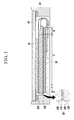
- FIG. 1 is a cross-sectional view of an organic light emitting diode (OLED) display according to a first exemplary embodiment.
- OLED organic light emitting diode
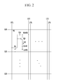
- FIG. 2 is an equivalent circuit of the organic light emitting diode (OLED) display according to the first exemplary embodiment.
- FIG. 3 is a perspective view of an impact absorption layer of the organic light emitting diode (OLED) display according to the first exemplary embodiment.
- FIG. 4 is a top plan view of the impact absorption layer of FIG. 3 .
- FIG. 5 is an enlarged view of a portion A of FIG. 4 .
- FIG. 6 is a top plan view of an impact absorption layer of an organic light emitting diode (OLED) display according to a second exemplary embodiment.
- OLED organic light emitting diode
- FIG. 7 is an enlarged view of a portion B of FIG. 6 .
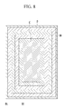
- FIG. 8 is a top plan view of an impact absorption layer of an organic light emitting diode (OLED) display according to a third exemplary embodiment.
- OLED organic light emitting diode
- OLED organic light emitting diode
- FIG. 2 is an equivalent circuit of the organic light emitting diode (OLED) display according to the first exemplary embodiment
- FIG. 1 is a cross-sectional view of the organic light emitting diode (OLED) display according to the first exemplary embodiment.
- an organic light emitting diode (OLED) display includes an organic light emitting panel 10 displaying an image, an exterior frame 20 protecting the organic light emitting panel 10 and receiving (housing) the organic light emitting panel 10 therein, a polarizing plate 30 attached on the organic light emitting panel 10 and preventing or reducing reflection of external light, a window 40 attached on the polarizing plate 30 and protecting the organic light emitting panel 10, and an impact absorption layer 50 installed between the exterior frame 20 and the organic light emitting panel 10 and protecting against an external impact.
- OLED organic light emitting diode
- the organic light emitting panel 10 includes a display substrate 100, an organic light emitting element 200 formed on the display substrate 100, a sealing member 300 covering the organic light emitting element 200, and a sealant 310 formed between a surrounding portion of the display substrate 100 and a surrounding portion of the sealing member 300.
- the impact absorption layer 50 is formed under the display substrate 100.
- the organic light emitting element 200 of the organic light emitting diode (OLED) display includes a plurality of signal lines 121, 171, and 172, and a plurality of pixels PX connected thereto and arranged substantially in a matrix.
- the signal lines include a plurality of gate signal lines 121 for transmitting scanning signals (or gate signals), a plurality of data lines 171 for transmitting data signals, and a plurality of driving voltage lines 172 for transmitting a driving voltage (ELVDD).
- the gate signal lines 121 extend substantially in a row direction and are substantially parallel to each other, and the data lines 171 extend substantially in a column direction and are substantially parallel to each other.
- Each pixel PX includes a switching thin film transistor Os, a driving thin film transistor Qd, a storage capacitor Cst, and an organic light emitting diode (OLED).
- Os switching thin film transistor
- driving thin film transistor Qd driving thin film transistor
- storage capacitor Cst storage capacitor
- OLED organic light emitting diode
- the thin film switching transistor Qs includes a control terminal, an input terminal, and an output terminal, in which the control terminal is connected to the scanning signal line 121, the input terminal is connected to the data line 171, and the output terminal is connected to the thin film driving transistor Qd.
- the thin film switching transistor Qs transmits the data signal received from the data line 171 to the driving transistor Qd in response to the scanning signal received from the scanning signal line 121.
- the thin film driving transistor Qd also includes a control terminal, an input terminal, and an output terminal, in which the control terminal is connected to the thin film switching transistor Os, the input terminal is connected to the driving voltage line 172, and the output terminal is connected to the organic light emitting element (OLED).
- the thin film driving transistor Qd applies an output current Id of which the magnitude varies according to the voltage applied between the control terminal and the output.
- the storage capacitor Cst is connected between the control terminal and the input terminal of the driving thin film transistor (Qd).
- the storage capacitor Cst stores the data signal applied to the control terminal of the driving transistor Qd and maintains the stored data signal even after the thin film switching transistor Os is turned off.
- the organic light emitting diode includes an anode connected to the output terminal of the driving thin film transistor (Qd) and a cathode connected to a common voltage (ELVSS).
- the organic light emitting element (OLED) emits light of which the intensity is varied according to the output current Id of the driving thin film transistor (Qd) thereby displaying an image.
- the switching thin film transistor (Qs) and the driving thin film transistor (Qd) are n-channel field effect transistors (FETs). However, at least one of the switching thin film transistor (Qs) and the driving thin film transistor (Qd) may be a p-channel field effect transistor. Also, a connection relation of the thin film transistors (Os, Qd), the capacitor Cst, and the organic light emitting diode (OLED) may be changed.
- FIG. 3 is a perspective view of an impact absorption layer of the organic light emitting diode (OLED) display according to the first exemplary embodiment
- FIG. 4 is a top plan view of the impact absorption layer of FIG. 3
- FIG. 5 is an enlarged view of a portion A of FIG. 4 .
- the impact absorption layer 50 includes a center impact absorption layer (C) formed at a position corresponding to a center of the display substrate 100, and a surrounding impact absorption layer (D) formed at a position corresponding to a surrounding portion of the display substrate 100 having a higher impact absorption ratio than the center impact absorption layer (C).
- the center impact absorption layer (C) includes an impact absorption agent 51 made of a porous polymer, and the surrounding impact absorption layer (D) includes the impact absorption agent 51 and an impact-absorbing opening 52 formed at the impact absorption agent 51.
- the impact absorption agent 51 elongates an impact time from the outside to smooth a maximum impact amount thereby preventing damage to the organic light emitting diode (OLED) display, and as an area occupied with the impact-absorbing opening 52 is increased in the impact absorption agent 51, the impact absorption amount is increased.
- the impact-absorbing opening 52 may be a plurality of impact-absorbing holes 52.
- the area ratio of the plurality of impact-absorbing holes 52 formed in the surrounding impact absorption layer (D) may decrease from the outer portion D1 of the surrounding impact absorption layer (D) to the inner portion D2 of the surrounding impact absorption layer (D).
- the size r1 of the plurality of impact-absorbing holes 52 may decrease from the outer portion D1 of the surrounding impact absorption layer (D) to the inner portion D2 of the surrounding impact absorption layer (D), and a hole interval w1 between a plurality of impact-absorbing hole 52 may increase from the outer portion D1 of the surrounding impact absorption layer (D) to the inner portion D2 of the surrounding impact absorption layer (D).
- the area ratio of the impact absorption agent 51 in the impact absorption layer 50 may increase from the position corresponding to the surrounding portion of the display substrate 100 to the center of the display substrate 100.
- the area ratio of the impact absorption agent 51 in the portion P1 of the center impact absorption layer (C) without the impact-absorbing hole 52 is 100 %
- the area ratio of the impact absorption agent 51 in the portion P2 of the surrounding impact absorption layer (D) formed with the largest impact-absorbing hole 52 is about 50 %, so the area ratio of the impact absorption agent 51 in the impact absorption layer 50 may be increased from the outer portion D1 of the surrounding impact absorption layer (D) to the inner portion D2 of the surrounding impact absorption layer (D).
- the area ratio of the impact absorption agent 51 in the impact absorption layer 50 may increase from the outer portion D1 of the surrounding impact absorption layer (D) to the inner portion D2 of the surrounding impact absorption layer (D), and the area ratio of the impact absorption agent 51 in the center impact absorption layer (C) may be larger than at the inner portion D2 of the surrounding impact absorption layer (D).
- the impact absorption ratio of the outer portion D1 of the surrounding impact absorption layer (D) is higher than the impact absorption ratio of the inner portion D2 of the surrounding impact absorption layer (D) such that damage to the surrounding portion of the display substrate 100 that is weak against the external impact may be prevented.
- the surrounding impact absorption layer (D) overlaps the sealant 310, and the width of the surrounding impact absorption layer (D) is larger than the width of the sealant 310 such that the surrounding impact absorption layer (D) under the sealant 310 having the high impact absorption ratio absorbs the external impact even when the external impact is concentrated at the sealant 310, thereby preventing the portion near the sealant 310 and the sealant 310 from being damaged.
- the impact-absorbing openings 52 are the plurality of impact-absorbing holes 52; however a second exemplary embodiment including the impact-absorbing openings 52 formed with a plurality of impact-absorbing opening lines 52 is possible.
- FIG. 6 is a top plan view of an impact absorption layer of an organic light emitting diode (OLED) display according to a second exemplary embodiment
- FIG. 7 is an enlarged view of a portion B of FIG. 6 .
- the second exemplary embodiment shown in FIG. 6 and FIG. 7 is substantially equivalent to the first exemplary embodiment shown in FIG. 1 to FIG. 5 except for a structure of the impact-absorbing openings such that the repeated description is omitted.
- the impact absorption layer 50 includes a center impact absorption layer (C) formed at the center of the display substrate 100, and a surrounding impact absorption layer (D) formed at the surrounding portion of the display substrate 100 and having a higher impact absorption ratio than the center impact absorption layer (C).
- the center impact absorption layer (C) includes the impact absorption agent 51 made of a porous polymer
- the surrounding impact absorption layer (D) includes the impact absorption agent 51 and the impact-absorbing openings 52 formed at the impact absorption agent 51.
- the impact-absorbing opening 52 may be a plurality of linear impact-absorbing opening lines 52, and a plurality of impact-absorbing opening lines 52 may be separated in parallel.
- the area ratio of a plurality of impact-absorbing lines 52 formed in surrounding impact absorption layer (D) may decrease from the outer portion D1 of the surrounding impact absorption layer (D) to the inner portion D2 of the surrounding impact absorption layer (D).
- the width r2 of a plurality of impact-absorbing opening lines 52 may decrease from the outer portion D1 of the surrounding impact absorption layer (D) to the inner portion D2 of the surrounding impact absorption layer (D), and the opening line interval w2 between a plurality of impact-absorbing opening lines 52 may increase from the outer portion D1 of the surrounding impact absorption layer (D) to the inner portion D2 of the surrounding impact absorption layer (D).
- the area ratio of the impact absorption agent 51 in the impact absorption layer 50 may increase from the position corresponding to the surrounding portion of the display substrate 100 to the center of the display substrate 100.
- the area ratio of the impact absorption agent 51 in the impact absorption layer 50 may increase from the outer portion D1 of the surrounding impact absorption layer (D) to the inner portion D2 of the surrounding impact absorption layer (D), and the area ratio of the impact absorption agent 51 in the center impact absorption layer (C) may be larger than at the inner portion D2 of the surrounding impact absorption layer (D).
- the impact absorption ratio of the outer portion D1 of the surrounding impact absorption layer (D) is higher than the impact absorption ratio of the inner portion D2 of the surrounding impact absorption layer (D) such that damage to the surrounding portion of the display substrate 100 that is weak against external impact may be prevented.
- the surrounding impact absorption layer (D) overlaps the sealant 310, and the width of the surrounding impact absorption layer (D) is larger than the width of the sealant 310 such that the surrounding impact absorption layer (D) under the sealant 310 having the high impact absorption ratio absorbs the external impact even when the external impact is concentrated at the sealant 310, thereby preventing the portion near the sealant 310 and the sealant 310 from being damaged.
- the impact-absorbing opening 52 is formed to increase the impact absorption ratio of the surrounding impact absorption layer (D), however the surrounding impact absorption layer may be formed with the impact absorption agent of a low density to increase the impact absorption ratio of the surrounding impact absorption layer (D) in the third exemplary embodiment.
- FIG. 8 is a top plan view of an impact absorption layer of an organic light emitting diode (OLED) display according to a third exemplary embodiment.
- OLED organic light emitting diode
- the third exemplary embodiment shown in FIG. 8 is substantially equivalent to the first exemplary embodiment shown in FIG. 1 to FIG. 5 except for a structure of the impact absorption layer such that the repeated description is omitted.
- the impact absorption layer 50 includes a center impact absorption layer (C) formed at the position corresponding to the center of the display substrate 100, and a surrounding impact absorption layer (D) formed at the position corresponding to the surrounding portion of the display substrate 100 and having a higher impact absorption ratio than the center impact absorption layer (C).
- the impact absorption agent in the center impact absorption layer (C) includes a high density impact absorption agent made of, e.g., a polymer of a high density
- the impact absorption agent in the surrounding impact absorption layer (D) includes a low density impact absorption agent made of, e.g., a porous polymer of a low density.
- the low density impact absorption agent is included in the impact absorption layer from the outer portion D1 of the surrounding impact absorption layer (D) to the inner portion D2 of the surrounding impact absorption layer (D).
- the high density impact absorption agent may be one of polyethylene terephthalate (PET), polyurethane, polystyrene, and polypropylene
- the low density impact absorption agent may be one of porous polypropylene, porous polyurethane, and porous acryl.
- the material density or area ratio of the impact absorption agent 51 in the impact absorption layer 50 may increase from the position corresponding to the surrounding portion of the display substrate 100 to the center of the display substrate 100.
- the impact absorption agent of the low density is included closer to the inner portion D2 of the surrounding impact absorption layer (D) from the outer portion D1 of the surrounding impact absorption layer (D) such that the area ratio of the impact absorption agent 51 in the impact absorption layer 50 may increase from the outer portion D1 of the surrounding impact absorption layer (D) to the inner portion D2 of the surrounding impact absorption layer (D).
- the center impact absorption layer (C) includes the high density impact absorption agent and the surrounding impact absorption layer (D) includes the low density impact absorption agent such that the area ratio of the impact absorption agent 51 in the center impact absorption layer (C) may be larger than the inner portion D2 of the surrounding impact absorption layer (D).
- the impact absorption ratio of the outer portion D1 of the surrounding impact absorption layer (D) is higher than the impact absorption ratio of the center impact absorption layer (C) such that damage to the surrounding portion of the display substrate 100 that is weak against external impact may be prevented.
Landscapes
- Physics & Mathematics (AREA)
- Optics & Photonics (AREA)
- Nonlinear Science (AREA)
- Mathematical Physics (AREA)
- Chemical & Material Sciences (AREA)
- Crystallography & Structural Chemistry (AREA)
- General Physics & Mathematics (AREA)
- Engineering & Computer Science (AREA)
- Microelectronics & Electronic Packaging (AREA)
- Electroluminescent Light Sources (AREA)
- Devices For Indicating Variable Information By Combining Individual Elements (AREA)
Abstract
Description
- The described technology relates generally to an organic light emitting diode (OLED) display.
- An organic light emitting diode (OLED) display includes an organic light emitting panel that includes an organic light emitting element. The organic light emitting element includes a plurality of OLEDs each formed of a hole injection electrode, an organic emission layer, and an electron injection electrode. Each OLED emits light by energy generated when excitons generated as electrons and holes are combined and dropped from an excited state to a ground state, and the OLED display displays an image by using the light.
- An organic light emitting panel including the organic light emitting element is installed in an exterior frame, and to prevent damage to the organic light emitting panel from an external impact, an impact absorption layer is installed between the exterior frame and the organic light emitting panel.
- However, even if the impact absorption layer is installed, damage may still be easily generated at a sealant portion near the organic light emitting panel that is relatively weak against external impact.
- The above information disclosed in this Background section is only for enhancement of understanding of the background of the described technology and therefore it may contain information that does not form the prior art that is already known in this country to a person of ordinary skill in the art.
- An aspect of an embodiment of the present invention is directed toward an organic light emitting diode (OLED) display that is protected against damage by an external impact.
- An organic light emitting diode (OLED) display according to the invention includes: a display substrate; an organic light emitting element formed on the substrate; a sealing member covering the organic light emitting element; a sealant formed between a surrounding portion of the display substrate and a surrounding portion of the sealing member; and an impact absorption layer formed under the display substrate, wherein an area ratio of an impact absorption agent formed in the impact absorption layer increases from the surrounding portion of the display substrate to a center of the display substrate.
- In an embodiment, the impact absorption layer may include a center impact absorption layer formed at a position corresponding to the center of the display substrate, and a surrounding impact absorption layer formed at a position corresponding to the surrounding portion of the display substrate and having a higher impact absorption ratio than the center impact absorption layer.
- The center impact absorption layer may include the impact absorption agent, and the surrounding impact absorption layer may include the impact absorption agent and an impact-absorbing opening formed at the impact absorption agent.
- The impact-absorbing opening may be a plurality of impact-absorbing holes.
- The area ratio of the plurality of impact-absorbing holes formed in the surrounding impact absorption layer may decrease from an outer portion of the surrounding impact absorption layer to an inner portion of the surrounding impact absorption layer.
- The size of the plurality of impact-absorbing holes may decrease from an outer portion of the surrounding impact absorption layer to an inner portion of the surrounding impact absorption layer.
- The hole interval between the plurality of impact-absorbing holes may increase from an outer portion of the surrounding impact absorption layer to an inner portion of the surrounding impact absorption layer.
- The impact-absorbing opening may be a plurality of impact-absorbing opening lines.
- The area ratio of the plurality of impact-absorbing opening lines formed in the surrounding impact absorption layer may decrease from an outer portion of the surrounding impact absorption layer to an inner portion of the surrounding impact absorption layer.
- The width of the plurality of impact-absorbing opening lines may decrease from the outer portion of the surrounding impact absorption layer to the inner portion of the surrounding impact absorption layer.
- The opening line interval between the plurality of impact-absorbing opening lines may increase from the outer portion of the surrounding impact absorption layer to the inner portion of the surrounding impact absorption layer.
- The impact absorption agent in the center impact absorption layer may include a high density impact absorption agent, and the impact absorption agent in the surrounding impact absorption layer may include a low density impact absorption agent.
- The low density impact absorption agent may be included in the pact absorption layer from an outer portion of the surrounding impact absorption layer to an inner portion of the surrounding impact absorption layer.
- The high density impact absorption agent may include one selected from polyethylene terephthalate (PET), polyurethane, polystyrene, and polypropylene.
- The low density impact absorption agent may include one selected from porous polypropylene, porous polyurethane, and porous acryl.
- The surrounding impact absorption layer may overlap the sealant, and the width of the surrounding impact absorption layer may be larger than the width of the sealant.
- Accordingly, in the organic light emitting diode (OLED) display according to an exemplary embodiment, the area ratio of the impact absorption agent formed in the impact absorption layer increases from the position corresponding to the surrounding portion of the display substrate to the position corresponding to the center of the display substrate such that the impact absorption ratio of the outer portion of the surrounding impact absorption layer is higher than the impact absorption ratio of the center impact absorption layer, and accordingly, damage to the surrounding portion of the display substrate that is weak against external impact may be prevented.
-
FIG. 1 is a cross-sectional view of an organic light emitting diode (OLED) display according to a first exemplary embodiment. -
FIG. 2 is an equivalent circuit of the organic light emitting diode (OLED) display according to the first exemplary embodiment. -
FIG. 3 is a perspective view of an impact absorption layer of the organic light emitting diode (OLED) display according to the first exemplary embodiment. -
FIG. 4 is a top plan view of the impact absorption layer ofFIG. 3 . -
FIG. 5 is an enlarged view of a portion A ofFIG. 4 . -
FIG. 6 is a top plan view of an impact absorption layer of an organic light emitting diode (OLED) display according to a second exemplary embodiment. -
FIG. 7 is an enlarged view of a portion B ofFIG. 6 . -
FIG. 8 is a top plan view of an impact absorption layer of an organic light emitting diode (OLED) display according to a third exemplary embodiment. - The present invention will be described more fully hereinafter with reference to the accompanying drawings, in which exemplary embodiments of the invention are shown. As those skilled in the art would realize, the described embodiments may be modified in various different ways, all without departing from the scope of the present invention.
- The drawings and description are to be regarded as illustrative in nature and not restrictive. Like reference numerals designate like elements throughout the specification.
- In order to clarify layers and regions, thicknesses and sizes thereof are exemplarily illustrated and thus the present invention is not limited thereto.
- In the drawings, the thickness of layers, films, panels, regions, etc., are exaggerated for clarity. In addition, in order to clarify some layers and some regions, thicknesses and sizes thereof are enlarged in the drawings. It will be understood that when an element such as a layer, film, region, or substrate is referred to as being "on" another element, it can be directly on the other element, or one or more intervening elements may also be present.
- In addition, unless explicitly described to the contrary, the word "comprise" and variations such as "comprises" or "comprising" will be understood to imply the inclusion of stated elements but not the exclusion of any other elements. Further, throughout the specification, "on" implies being positioned above or below a target element and does not imply being necessarily positioned on the top on the basis of a gravity direction.
- Now, an organic light emitting diode (OLED) display according to a first exemplary embodiment will be described with reference to
FIG. 1 to FIG. 5 . -
FIG. 2 is an equivalent circuit of the organic light emitting diode (OLED) display according to the first exemplary embodiment, andFIG. 1 is a cross-sectional view of the organic light emitting diode (OLED) display according to the first exemplary embodiment. - As shown in
FIG. 1 , an organic light emitting diode (OLED) display according to the first exemplary embodiment includes an organiclight emitting panel 10 displaying an image, anexterior frame 20 protecting the organiclight emitting panel 10 and receiving (housing) the organiclight emitting panel 10 therein, a polarizingplate 30 attached on the organiclight emitting panel 10 and preventing or reducing reflection of external light, awindow 40 attached on the polarizingplate 30 and protecting the organiclight emitting panel 10, and animpact absorption layer 50 installed between theexterior frame 20 and the organiclight emitting panel 10 and protecting against an external impact. - The organic
light emitting panel 10 includes adisplay substrate 100, an organiclight emitting element 200 formed on thedisplay substrate 100, asealing member 300 covering the organiclight emitting element 200, and asealant 310 formed between a surrounding portion of thedisplay substrate 100 and a surrounding portion of the sealingmember 300. Theimpact absorption layer 50 is formed under thedisplay substrate 100. - As shown in
FIG. 2 , the organiclight emitting element 200 of the organic light emitting diode (OLED) display according to the first exemplary embodiment includes a plurality ofsignal lines - The signal lines include a plurality of
gate signal lines 121 for transmitting scanning signals (or gate signals), a plurality ofdata lines 171 for transmitting data signals, and a plurality ofdriving voltage lines 172 for transmitting a driving voltage (ELVDD). Thegate signal lines 121 extend substantially in a row direction and are substantially parallel to each other, and thedata lines 171 extend substantially in a column direction and are substantially parallel to each other. - Each pixel PX includes a switching thin film transistor Os, a driving thin film transistor Qd, a storage capacitor Cst, and an organic light emitting diode (OLED).
- The thin film switching transistor Qs includes a control terminal, an input terminal, and an output terminal, in which the control terminal is connected to the
scanning signal line 121, the input terminal is connected to thedata line 171, and the output terminal is connected to the thin film driving transistor Qd. The thin film switching transistor Qs transmits the data signal received from thedata line 171 to the driving transistor Qd in response to the scanning signal received from thescanning signal line 121. - The thin film driving transistor Qd also includes a control terminal, an input terminal, and an output terminal, in which the control terminal is connected to the thin film switching transistor Os, the input terminal is connected to the
driving voltage line 172, and the output terminal is connected to the organic light emitting element (OLED). The thin film driving transistor Qd applies an output current Id of which the magnitude varies according to the voltage applied between the control terminal and the output. - The storage capacitor Cst is connected between the control terminal and the input terminal of the driving thin film transistor (Qd). The storage capacitor Cst stores the data signal applied to the control terminal of the driving transistor Qd and maintains the stored data signal even after the thin film switching transistor Os is turned off.
- The organic light emitting diode (OLED) includes an anode connected to the output terminal of the driving thin film transistor (Qd) and a cathode connected to a common voltage (ELVSS). The organic light emitting element (OLED) emits light of which the intensity is varied according to the output current Id of the driving thin film transistor (Qd) thereby displaying an image.
- The switching thin film transistor (Qs) and the driving thin film transistor (Qd) are n-channel field effect transistors (FETs). However, at least one of the switching thin film transistor (Qs) and the driving thin film transistor (Qd) may be a p-channel field effect transistor. Also, a connection relation of the thin film transistors (Os, Qd), the capacitor Cst, and the organic light emitting diode (OLED) may be changed.
- Next, the impact absorption layer will be described with reference to
FIG. 3 to FIG. 5 . -
FIG. 3 is a perspective view of an impact absorption layer of the organic light emitting diode (OLED) display according to the first exemplary embodiment,FIG. 4 is a top plan view of the impact absorption layer ofFIG. 3 , andFIG. 5 is an enlarged view of a portion A ofFIG. 4 . - As shown in
FIG. 3 to FIG. 5 , theimpact absorption layer 50 includes a center impact absorption layer (C) formed at a position corresponding to a center of thedisplay substrate 100, and a surrounding impact absorption layer (D) formed at a position corresponding to a surrounding portion of thedisplay substrate 100 having a higher impact absorption ratio than the center impact absorption layer (C). - The center impact absorption layer (C) includes an
impact absorption agent 51 made of a porous polymer, and the surrounding impact absorption layer (D) includes theimpact absorption agent 51 and an impact-absorbingopening 52 formed at theimpact absorption agent 51. Theimpact absorption agent 51 elongates an impact time from the outside to smooth a maximum impact amount thereby preventing damage to the organic light emitting diode (OLED) display, and as an area occupied with the impact-absorbingopening 52 is increased in theimpact absorption agent 51, the impact absorption amount is increased. The impact-absorbingopening 52 may be a plurality of impact-absorbingholes 52. - The area ratio of the plurality of impact-absorbing
holes 52 formed in the surrounding impact absorption layer (D) may decrease from the outer portion D1 of the surrounding impact absorption layer (D) to the inner portion D2 of the surrounding impact absorption layer (D). - Also, the size r1 of the plurality of impact-absorbing
holes 52 may decrease from the outer portion D1 of the surrounding impact absorption layer (D) to the inner portion D2 of the surrounding impact absorption layer (D), and a hole interval w1 between a plurality of impact-absorbinghole 52 may increase from the outer portion D1 of the surrounding impact absorption layer (D) to the inner portion D2 of the surrounding impact absorption layer (D). - Accordingly, the area ratio of the
impact absorption agent 51 in theimpact absorption layer 50 may increase from the position corresponding to the surrounding portion of thedisplay substrate 100 to the center of thedisplay substrate 100. For example, as shown inFIG. 4 , the area ratio of theimpact absorption agent 51 in the portion P1 of the center impact absorption layer (C) without the impact-absorbinghole 52 is 100 %, and the area ratio of theimpact absorption agent 51 in the portion P2 of the surrounding impact absorption layer (D) formed with the largest impact-absorbinghole 52 is about 50 %, so the area ratio of theimpact absorption agent 51 in theimpact absorption layer 50 may be increased from the outer portion D1 of the surrounding impact absorption layer (D) to the inner portion D2 of the surrounding impact absorption layer (D). - As described above, the area ratio of the
impact absorption agent 51 in theimpact absorption layer 50 may increase from the outer portion D1 of the surrounding impact absorption layer (D) to the inner portion D2 of the surrounding impact absorption layer (D), and the area ratio of theimpact absorption agent 51 in the center impact absorption layer (C) may be larger than at the inner portion D2 of the surrounding impact absorption layer (D). - Accordingly, the impact absorption ratio of the outer portion D1 of the surrounding impact absorption layer (D) is higher than the impact absorption ratio of the inner portion D2 of the surrounding impact absorption layer (D) such that damage to the surrounding portion of the
display substrate 100 that is weak against the external impact may be prevented. - Here, the surrounding impact absorption layer (D) overlaps the
sealant 310, and the width of the surrounding impact absorption layer (D) is larger than the width of thesealant 310 such that the surrounding impact absorption layer (D) under thesealant 310 having the high impact absorption ratio absorbs the external impact even when the external impact is concentrated at thesealant 310, thereby preventing the portion near thesealant 310 and thesealant 310 from being damaged. - Meanwhile, in the first exemplary embodiment, the impact-absorbing
openings 52 are the plurality of impact-absorbingholes 52; however a second exemplary embodiment including the impact-absorbingopenings 52 formed with a plurality of impact-absorbingopening lines 52 is possible. -
FIG. 6 is a top plan view of an impact absorption layer of an organic light emitting diode (OLED) display according to a second exemplary embodiment, andFIG. 7 is an enlarged view of a portion B ofFIG. 6 . - The second exemplary embodiment shown in
FIG. 6 andFIG. 7 is substantially equivalent to the first exemplary embodiment shown inFIG. 1 to FIG. 5 except for a structure of the impact-absorbing openings such that the repeated description is omitted. - As shown in
FIG. 1 ,FIG. 6 , andFIG. 7 , theimpact absorption layer 50 includes a center impact absorption layer (C) formed at the center of thedisplay substrate 100, and a surrounding impact absorption layer (D) formed at the surrounding portion of thedisplay substrate 100 and having a higher impact absorption ratio than the center impact absorption layer (C). The center impact absorption layer (C) includes theimpact absorption agent 51 made of a porous polymer, and the surrounding impact absorption layer (D) includes theimpact absorption agent 51 and the impact-absorbingopenings 52 formed at theimpact absorption agent 51. Here, the impact-absorbingopening 52 may be a plurality of linear impact-absorbingopening lines 52, and a plurality of impact-absorbingopening lines 52 may be separated in parallel. - The area ratio of a plurality of impact-absorbing
lines 52 formed in surrounding impact absorption layer (D) may decrease from the outer portion D1 of the surrounding impact absorption layer (D) to the inner portion D2 of the surrounding impact absorption layer (D). - Also, the width r2 of a plurality of impact-absorbing
opening lines 52 may decrease from the outer portion D1 of the surrounding impact absorption layer (D) to the inner portion D2 of the surrounding impact absorption layer (D), and the opening line interval w2 between a plurality of impact-absorbingopening lines 52 may increase from the outer portion D1 of the surrounding impact absorption layer (D) to the inner portion D2 of the surrounding impact absorption layer (D). - Accordingly, the area ratio of the
impact absorption agent 51 in theimpact absorption layer 50 may increase from the position corresponding to the surrounding portion of thedisplay substrate 100 to the center of thedisplay substrate 100. In more detail, the area ratio of theimpact absorption agent 51 in theimpact absorption layer 50 may increase from the outer portion D1 of the surrounding impact absorption layer (D) to the inner portion D2 of the surrounding impact absorption layer (D), and the area ratio of theimpact absorption agent 51 in the center impact absorption layer (C) may be larger than at the inner portion D2 of the surrounding impact absorption layer (D). Accordingly, the impact absorption ratio of the outer portion D1 of the surrounding impact absorption layer (D) is higher than the impact absorption ratio of the inner portion D2 of the surrounding impact absorption layer (D) such that damage to the surrounding portion of thedisplay substrate 100 that is weak against external impact may be prevented. - Here, the surrounding impact absorption layer (D) overlaps the
sealant 310, and the width of the surrounding impact absorption layer (D) is larger than the width of thesealant 310 such that the surrounding impact absorption layer (D) under thesealant 310 having the high impact absorption ratio absorbs the external impact even when the external impact is concentrated at thesealant 310, thereby preventing the portion near thesealant 310 and thesealant 310 from being damaged. - Meanwhile, in the first exemplary embodiment, the impact-absorbing
opening 52 is formed to increase the impact absorption ratio of the surrounding impact absorption layer (D), however the surrounding impact absorption layer may be formed with the impact absorption agent of a low density to increase the impact absorption ratio of the surrounding impact absorption layer (D) in the third exemplary embodiment. -
FIG. 8 is a top plan view of an impact absorption layer of an organic light emitting diode (OLED) display according to a third exemplary embodiment. - The third exemplary embodiment shown in
FIG. 8 is substantially equivalent to the first exemplary embodiment shown inFIG. 1 to FIG. 5 except for a structure of the impact absorption layer such that the repeated description is omitted. - As shown in
FIG. 1 andFIG. 8 , theimpact absorption layer 50 includes a center impact absorption layer (C) formed at the position corresponding to the center of thedisplay substrate 100, and a surrounding impact absorption layer (D) formed at the position corresponding to the surrounding portion of thedisplay substrate 100 and having a higher impact absorption ratio than the center impact absorption layer (C). The impact absorption agent in the center impact absorption layer (C) includes a high density impact absorption agent made of, e.g., a polymer of a high density, and the impact absorption agent in the surrounding impact absorption layer (D) includes a low density impact absorption agent made of, e.g., a porous polymer of a low density. Also, the low density impact absorption agent is included in the impact absorption layer from the outer portion D1 of the surrounding impact absorption layer (D) to the inner portion D2 of the surrounding impact absorption layer (D). - The high density impact absorption agent may be one of polyethylene terephthalate (PET), polyurethane, polystyrene, and polypropylene, and the low density impact absorption agent may be one of porous polypropylene, porous polyurethane, and porous acryl.
- Accordingly, the material density or area ratio of the
impact absorption agent 51 in theimpact absorption layer 50 may increase from the position corresponding to the surrounding portion of thedisplay substrate 100 to the center of thedisplay substrate 100. In more detail, the impact absorption agent of the low density is included closer to the inner portion D2 of the surrounding impact absorption layer (D) from the outer portion D1 of the surrounding impact absorption layer (D) such that the area ratio of theimpact absorption agent 51 in theimpact absorption layer 50 may increase from the outer portion D1 of the surrounding impact absorption layer (D) to the inner portion D2 of the surrounding impact absorption layer (D). Also, the center impact absorption layer (C) includes the high density impact absorption agent and the surrounding impact absorption layer (D) includes the low density impact absorption agent such that the area ratio of theimpact absorption agent 51 in the center impact absorption layer (C) may be larger than the inner portion D2 of the surrounding impact absorption layer (D). - Accordingly, the impact absorption ratio of the outer portion D1 of the surrounding impact absorption layer (D) is higher than the impact absorption ratio of the center impact absorption layer (C) such that damage to the surrounding portion of the
display substrate 100 that is weak against external impact may be prevented. - While this disclosure has been described in connection with what is presently considered to be practical exemplary embodiments, it is to be understood that the invention is not limited to the disclosed embodiments, but, on the contrary, is intended to cover various modifications and equivalent arrangements included within the scope of the appended claims, and equivalents thereof.
-
50: impact absorption layer 51: impact absorption agent 52: impact-absorbing opening 310: sealant C: center impact absorption layer D: surrounding impact absorption layer 100: display substrate 200: organic light emitting element 300: sealing member 310 sealant
Claims (17)
- An organic light emitting diode (OLED) display comprising:a display substrate (100);an organic light emitting element (200) on the substrate (100);a sealing member (300) covering the organic light emitting element (200);a sealant (310) between a surrounding portion of the display substrate (100) and a surrounding portion of the sealing member (300); andan impact absorption layer (50) under the display substrate (100),wherein an area ratio of an impact absorption agent (51) in the impact absorption layer (50) increases from the surrounding portion of the display substrate (100) to a center of the display substrate (100).
- The organic light emitting diode (OLED) display of claim 1, wherein
the impact absorption layer (50) comprises
a center impact absorption layer (C) at a position corresponding to the center of the display substrate (100), and
a surrounding impact absorption layer (D) at a position corresponding to the surrounding portion of the display substrate (100) and having a higher impact absorption ratio than the center impact absorption layer (C). - The organic light emitting diode (OLED) display of claim 2, wherein
the center impact absorption layer (C) comprises the impact absorption agent (51), and the surrounding impact absorption layer (D) comprises the impact absorption agent (51) and an impact-absorbing opening (52) formed at the impact absorption agent (51). - The organic light emitting diode (OLED) display of claim 3, wherein
the impact-absorbing opening (52) is a plurality of impact-absorbing holes. - The organic light emitting diode (OLED) display of claim 4, wherein
the area ratio of the plurality of impact-absorbing holes (52) in the surrounding impact absorption layer (D) decreases from an outer portion of the surrounding impact absorption layer (D) to an inner portion of the surrounding impact absorption layer (D). - The organic light emitting diode (OLED) display of claim 4 or 5, wherein
the size of the plurality of impact-absorbing holes (52) decreases from an outer portion of the surrounding impact absorption layer (D) to an inner portion of the surrounding impact absorption layer (D). - The organic light emitting diode (OLED) display of claim 4, 5 or 6, wherein
the hole interval between the plurality of impact-absorbing holes (52) increases from an outer portion of the surrounding impact absorption layer (D) to an inner portion of the surrounding impact absorption layer (D). - The organic light emitting diode (OLED) display of one of claims 3 to 7, wherein the impact-absorbing opening (52) is a plurality of impact-absorbing opening lines.
- The organic light emitting diode (OLED) display of claim 8, wherein
the area ratio of the plurality of impact-absorbing opening lines (52) in the surrounding impact absorption layer (D) decreases from an outer portion of the surrounding impact absorption layer (D) to an inner portion of the surrounding impact absorption layer (D). - The organic light emitting diode (OLED) display of claim 8 or 9, wherein
the width of the plurality of impact-absorbing opening lines (52) decreases from an outer portion of the surrounding impact absorption layer (D) to an inner portion of the surrounding impact absorption layer (D). - The organic light emitting diode (OLED) display of one of claims 8 to 10, wherein
the opening line interval between the plurality of impact-absorbing opening lines (52) increases from an outer portion of the surrounding impact absorption layer (D) to an inner portion of the surrounding impact absorption layer (D). - The organic light emitting diode (OLED) display of one of claims 2 to 11, wherein
the impact absorption agent (51) in the center impact absorption layer (C) includes a high density impact absorption agent, and
the impact absorption agent (51) in the surrounding impact absorption layer (D) includes a low density impact absorption agent. - The organic light emitting diode (OLED) display of claim 12, wherein
the low density impact absorption agent is included in the impact absorption layer from an outer portion of the surrounding impact absorption layer (D) to an inner portion of the surrounding impact absorption layer (D). - The organic light emitting diode (OLED) display of claim 13, wherein
the high density impact absorption agent comprises one selected from polyethylene terephthalate (PET), polyurethane, polystyrene, and polypropylene. - The organic light emitting diode (OLED) display of claim 13 or 14, wherein
the low density impact absorption agent comprises one selected from porous polypropylene, porous polyurethane, and porous acryl. - The organic light emitting diode (OLED) display of one of claims 2 to 15, wherein the surrounding impact absorption layer (D) overlaps the sealant (310).
- The organic light emitting diode (OLED) display of claim 16, wherein
the width of the surrounding impact absorption layer (D) is larger than the width of the sealant (310).
Applications Claiming Priority (1)
| Application Number | Priority Date | Filing Date | Title |
|---|---|---|---|
| KR1020120103952A KR101973023B1 (en) | 2012-09-19 | 2012-09-19 | Organic light emitting diode display |
Publications (2)
| Publication Number | Publication Date |
|---|---|
| EP2712002A2 true EP2712002A2 (en) | 2014-03-26 |
| EP2712002A3 EP2712002A3 (en) | 2016-11-16 |
Family
ID=49117742
Family Applications (1)
| Application Number | Title | Priority Date | Filing Date |
|---|---|---|---|
| EP13183456.6A Withdrawn EP2712002A3 (en) | 2012-09-19 | 2013-09-09 | Organic light emitting diode display |
Country Status (5)
| Country | Link |
|---|---|
| US (1) | US8841761B2 (en) |
| EP (1) | EP2712002A3 (en) |
| KR (1) | KR101973023B1 (en) |
| CN (1) | CN103681759B (en) |
| TW (1) | TWI581421B (en) |
Families Citing this family (11)
| Publication number | Priority date | Publication date | Assignee | Title |
|---|---|---|---|---|
| CN104134660A (en) * | 2014-07-07 | 2014-11-05 | 京东方科技集团股份有限公司 | Support device and flexible display device |
| CN105609006B (en) * | 2015-12-31 | 2020-05-19 | 京东方科技集团股份有限公司 | a flexible device |
| KR102591754B1 (en) * | 2016-09-09 | 2023-10-20 | 삼성디스플레이 주식회사 | Cover panel and display device comprising the same |
| KR102653753B1 (en) * | 2016-11-16 | 2024-04-02 | 삼성디스플레이 주식회사 | Window for felxible display device and felxible display device having thereof |
| KR102334411B1 (en) * | 2017-07-25 | 2021-12-03 | 삼성디스플레이 주식회사 | Display apparatus and manufacturing the same |
| KR102392989B1 (en) | 2017-12-05 | 2022-04-29 | 엘지디스플레이 주식회사 | Flexible display device |
| CN108963075B (en) * | 2018-07-23 | 2022-03-22 | 广州国显科技有限公司 | Support film, preparation method thereof, display module and display panel |
| CN109036136A (en) * | 2018-08-10 | 2018-12-18 | 云谷(固安)科技有限公司 | Support membrane, display device and preparation method thereof |
| JP7298161B2 (en) * | 2019-01-18 | 2023-06-27 | Agc株式会社 | SUBSTRATE WITH FUNCTIONAL LAYER AND MANUFACTURING METHOD THEREOF |
| WO2022050697A1 (en) * | 2020-09-02 | 2022-03-10 | 주식회사 엘지화학 | Buffer film |
| CN114694484B (en) * | 2020-12-25 | 2023-07-07 | 华为技术有限公司 | Backplane and its preparation method, display module and terminal |
Citations (4)
| Publication number | Priority date | Publication date | Assignee | Title |
|---|---|---|---|---|
| EP2110842A2 (en) * | 2008-04-14 | 2009-10-21 | Samsung SDI Co., Ltd. | Film unit and plasma display panel having the same |
| US20110279961A1 (en) * | 2010-05-14 | 2011-11-17 | Anna-Katrina Shedletsky | Shock mounting cover glass in consumer electronics devices |
| US20110291553A1 (en) * | 2010-05-28 | 2011-12-01 | Chan-Kyoung Moon | Organic light emitting diode display |
| US20120056530A1 (en) * | 2010-09-02 | 2012-03-08 | Samsung Mobile Display Co., Ltd. | Organic Light-emitting Display Device and Method of Manufacturing the Same |
Family Cites Families (19)
| Publication number | Priority date | Publication date | Assignee | Title |
|---|---|---|---|---|
| US4851286A (en) * | 1986-11-18 | 1989-07-25 | United Foam Plastics | Foamed plastic cushioning materials |
| KR100364763B1 (en) * | 2000-07-05 | 2002-12-16 | 엘지전자 주식회사 | organic electroluminescence device |
| JP4020382B2 (en) * | 2000-11-06 | 2007-12-12 | 電気化学工業株式会社 | Conductive polypropylene resin foam sheet and container |
| JP2003029647A (en) * | 2001-07-12 | 2003-01-31 | Hitachi Ltd | Plasma display device |
| JP3943437B2 (en) * | 2002-05-10 | 2007-07-11 | アルプス電気株式会社 | Liquid crystal display |
| ATE360977T1 (en) * | 2004-09-03 | 2007-05-15 | Research In Motion Ltd | SHOCKPROOF MOUNTING DEVICE FOR SMALL DISPLAY SCREEN |
| KR20060033217A (en) | 2004-10-14 | 2006-04-19 | 브이케이 주식회사 | Mobile communication terminal filled with shock absorber and its filling method |
| KR20070034806A (en) | 2005-09-26 | 2007-03-29 | 삼성전자주식회사 | Liquid Crystal Display With Backlight Unit |
| KR101260988B1 (en) | 2006-06-19 | 2013-05-06 | 엘지디스플레이 주식회사 | Reflector sheet for back light uint and back light uint using the same |
| KR100922357B1 (en) * | 2008-02-04 | 2009-10-21 | 삼성모바일디스플레이주식회사 | Organic light emitting display |
| JP2009251550A (en) * | 2008-04-11 | 2009-10-29 | Epson Imaging Devices Corp | Electrooptical device, input device, and electronic apparatus |
| KR101296912B1 (en) * | 2008-11-17 | 2013-08-14 | 엘지디스플레이 주식회사 | Back Light Unit And Liquid Crystal Display Using It |
| JP5676590B2 (en) | 2009-06-18 | 2015-02-25 | スリーエム イノベイティブ プロパティズ カンパニー | Polymer foam |
| KR101704686B1 (en) * | 2010-04-01 | 2017-02-09 | 삼성디스플레이 주식회사 | Organic light emitting display apparatus |
| KR101127592B1 (en) * | 2010-04-06 | 2012-03-23 | 삼성모바일디스플레이주식회사 | Organinc light emitting display device and electronic equipment having the same |
| WO2011125307A1 (en) * | 2010-04-09 | 2011-10-13 | シャープ株式会社 | Display apparatus |
| US8780579B2 (en) * | 2011-01-05 | 2014-07-15 | Samsung Display Co., Ltd. | Organic light emitting diode display |
| KR20130060885A (en) * | 2011-11-30 | 2013-06-10 | 삼성디스플레이 주식회사 | Cushion sheet and display device having the same |
| US9419065B2 (en) * | 2012-08-07 | 2016-08-16 | Apple Inc. | Flexible displays |
-
2012
- 2012-09-19 KR KR1020120103952A patent/KR101973023B1/en active Active
-
2013
- 2013-06-04 US US13/910,042 patent/US8841761B2/en active Active
- 2013-07-26 TW TW102126850A patent/TWI581421B/en active
- 2013-09-09 EP EP13183456.6A patent/EP2712002A3/en not_active Withdrawn
- 2013-09-09 CN CN201310406879.5A patent/CN103681759B/en active Active
Patent Citations (4)
| Publication number | Priority date | Publication date | Assignee | Title |
|---|---|---|---|---|
| EP2110842A2 (en) * | 2008-04-14 | 2009-10-21 | Samsung SDI Co., Ltd. | Film unit and plasma display panel having the same |
| US20110279961A1 (en) * | 2010-05-14 | 2011-11-17 | Anna-Katrina Shedletsky | Shock mounting cover glass in consumer electronics devices |
| US20110291553A1 (en) * | 2010-05-28 | 2011-12-01 | Chan-Kyoung Moon | Organic light emitting diode display |
| US20120056530A1 (en) * | 2010-09-02 | 2012-03-08 | Samsung Mobile Display Co., Ltd. | Organic Light-emitting Display Device and Method of Manufacturing the Same |
Also Published As
| Publication number | Publication date |
|---|---|
| US8841761B2 (en) | 2014-09-23 |
| EP2712002A3 (en) | 2016-11-16 |
| CN103681759A (en) | 2014-03-26 |
| TWI581421B (en) | 2017-05-01 |
| TW201413938A (en) | 2014-04-01 |
| US20140077181A1 (en) | 2014-03-20 |
| KR20140037601A (en) | 2014-03-27 |
| KR101973023B1 (en) | 2019-04-29 |
| CN103681759B (en) | 2018-02-13 |
Similar Documents
| Publication | Publication Date | Title |
|---|---|---|
| US8841761B2 (en) | Organic light emitting diode display | |
| US11111347B2 (en) | Organic light emitting device and manufacturing method thereof | |
| US12250868B2 (en) | Display apparatus | |
| US9000428B2 (en) | Organic light emitting diode display | |
| US8866170B2 (en) | Light emitting diode display | |
| US7898174B2 (en) | Organic electroluminescent display device with moisture resistant structural body including adhesive layer | |
| US7944140B2 (en) | Organic light emitting display and method of manufacturing the same | |
| US8415872B2 (en) | Organic light emitting diode display device | |
| US8492975B2 (en) | Organic light emitting diode display | |
| US20160260790A1 (en) | Thin film transistor array substrate and organic light-emitting diode display | |
| US8987773B2 (en) | Organic light emitting diode display | |
| KR102044314B1 (en) | Organic light emitting diode display | |
| US8796727B2 (en) | Organic light emitting diode display | |
| CN104377313A (en) | Organic light emitting diode display | |
| KR102061793B1 (en) | Organic light emitting diode display | |
| US8907873B2 (en) | Organic light emitting display panel and method for driving the same | |
| KR20160014815A (en) | Organic light emitting decvice |
Legal Events
| Date | Code | Title | Description |
|---|---|---|---|
| PUAI | Public reference made under article 153(3) epc to a published international application that has entered the european phase |
Free format text: ORIGINAL CODE: 0009012 |
|
| AK | Designated contracting states |
Kind code of ref document: A2 Designated state(s): AL AT BE BG CH CY CZ DE DK EE ES FI FR GB GR HR HU IE IS IT LI LT LU LV MC MK MT NL NO PL PT RO RS SE SI SK SM TR |
|
| AX | Request for extension of the european patent |
Extension state: BA ME |
|
| RAP1 | Party data changed (applicant data changed or rights of an application transferred) |
Owner name: SAMSUNG DISPLAY CO., LTD. |
|
| PUAL | Search report despatched |
Free format text: ORIGINAL CODE: 0009013 |
|
| AK | Designated contracting states |
Kind code of ref document: A3 Designated state(s): AL AT BE BG CH CY CZ DE DK EE ES FI FR GB GR HR HU IE IS IT LI LT LU LV MC MK MT NL NO PL PT RO RS SE SI SK SM TR |
|
| AX | Request for extension of the european patent |
Extension state: BA ME |
|
| RIC1 | Information provided on ipc code assigned before grant |
Ipc: G06F 1/16 20060101ALI20161010BHEP Ipc: H01L 51/52 20060101AFI20161010BHEP Ipc: H05K 5/02 20060101ALI20161010BHEP Ipc: H04N 5/64 20060101ALI20161010BHEP Ipc: H04N 5/645 20060101ALI20161010BHEP Ipc: H01L 27/30 20060101ALI20161010BHEP Ipc: B65D 85/38 20060101ALI20161010BHEP Ipc: G02F 1/1335 20060101ALI20161010BHEP Ipc: H01L 51/00 20060101ALI20161010BHEP |
|
| STAA | Information on the status of an ep patent application or granted ep patent |
Free format text: STATUS: REQUEST FOR EXAMINATION WAS MADE |
|
| 17P | Request for examination filed |
Effective date: 20170509 |
|
| RBV | Designated contracting states (corrected) |
Designated state(s): AL AT BE BG CH CY CZ DE DK EE ES FI FR GB GR HR HU IE IS IT LI LT LU LV MC MK MT NL NO PL PT RO RS SE SI SK SM TR |
|
| GRAP | Despatch of communication of intention to grant a patent |
Free format text: ORIGINAL CODE: EPIDOSNIGR1 |
|
| STAA | Information on the status of an ep patent application or granted ep patent |
Free format text: STATUS: GRANT OF PATENT IS INTENDED |
|
| RIC1 | Information provided on ipc code assigned before grant |
Ipc: H01L 27/32 20060101AFI20190423BHEP Ipc: H05K 5/02 20060101ALI20190423BHEP Ipc: B65D 85/38 20060101ALI20190423BHEP Ipc: G06F 1/16 20060101ALI20190423BHEP Ipc: H04N 5/645 20060101ALI20190423BHEP Ipc: H01L 51/52 20060101ALI20190423BHEP Ipc: H04N 5/64 20060101ALI20190423BHEP Ipc: G02F 1/1335 20060101ALI20190423BHEP |
|
| INTG | Intention to grant announced |
Effective date: 20190527 |
|
| STAA | Information on the status of an ep patent application or granted ep patent |
Free format text: STATUS: THE APPLICATION IS DEEMED TO BE WITHDRAWN |
|
| 18D | Application deemed to be withdrawn |
Effective date: 20191008 |