EP2711786A2 - Electronic timepiece with internal antenna - Google Patents
Electronic timepiece with internal antenna Download PDFInfo
- Publication number
- EP2711786A2 EP2711786A2 EP13185300.4A EP13185300A EP2711786A2 EP 2711786 A2 EP2711786 A2 EP 2711786A2 EP 13185300 A EP13185300 A EP 13185300A EP 2711786 A2 EP2711786 A2 EP 2711786A2
- Authority
- EP
- European Patent Office
- Prior art keywords
- antenna
- electronic timepiece
- disposed
- driven element
- dielectric
- Prior art date
- Legal status (The legal status is an assumption and is not a legal conclusion. Google has not performed a legal analysis and makes no representation as to the accuracy of the status listed.)
- Granted
Links
Images




Classifications
-
- G—PHYSICS
- G04—HOROLOGY
- G04R—RADIO-CONTROLLED TIME-PIECES
- G04R60/00—Constructional details
- G04R60/06—Antennas attached to or integrated in clock or watch bodies
- G04R60/10—Antennas attached to or integrated in clock or watch bodies inside cases
-
- G—PHYSICS
- G01—MEASURING; TESTING
- G01S—RADIO DIRECTION-FINDING; RADIO NAVIGATION; DETERMINING DISTANCE OR VELOCITY BY USE OF RADIO WAVES; LOCATING OR PRESENCE-DETECTING BY USE OF THE REFLECTION OR RERADIATION OF RADIO WAVES; ANALOGOUS ARRANGEMENTS USING OTHER WAVES
- G01S19/00—Satellite radio beacon positioning systems; Determining position, velocity or attitude using signals transmitted by such systems
- G01S19/01—Satellite radio beacon positioning systems transmitting time-stamped messages, e.g. GPS [Global Positioning System], GLONASS [Global Orbiting Navigation Satellite System] or GALILEO
- G01S19/13—Receivers
- G01S19/14—Receivers specially adapted for specific applications
-
- H—ELECTRICITY
- H01—ELECTRIC ELEMENTS
- H01Q—ANTENNAS, i.e. RADIO AERIALS
- H01Q1/00—Details of, or arrangements associated with, antennas
- H01Q1/27—Adaptation for use in or on movable bodies
- H01Q1/273—Adaptation for carrying or wearing by persons or animals
-
- H—ELECTRICITY
- H01—ELECTRIC ELEMENTS
- H01Q—ANTENNAS, i.e. RADIO AERIALS
- H01Q1/00—Details of, or arrangements associated with, antennas
- H01Q1/44—Details of, or arrangements associated with, antennas using equipment having another main function to serve additionally as an antenna, e.g. means for giving an antenna an aesthetic aspect
-
- H—ELECTRICITY
- H01—ELECTRIC ELEMENTS
- H01Q—ANTENNAS, i.e. RADIO AERIALS
- H01Q7/00—Loop antennas with a substantially uniform current distribution around the loop and having a directional radiation pattern in a plane perpendicular to the plane of the loop
Definitions
- the present invention relates to an electronic timepiece with an internal antenna.
- Japanese Unexamined Patent Appl. Pub. JP-A-H09-307329 teaches an electronic timepiece having a loop antenna 20 formed along the outside circumference below the crystal 5, and lugs 2 for attaching a wrist band at the 12:00 and 6:00 positions of the case 1. As shown in FIG. 1 of JP-A-H09-307329 , an electrode 21 for the antenna 20 is also disposed near one of the lugs 2, that is, the electrode 21 of the antenna 20 is disposed at 12:00 or 6:00.
- JP-A-H09-247006 discloses disposing an antenna 11 that functions as a loop antenna in unison with the case 17 of a wrist-worn receiver. As shown in FIG. 1 of JP-A-H09-247006 , lugs 21 for attaching a band 41 are formed at two locations on the case 17, and a feed opening 15 for the antenna 11 is disposed near one set of lugs 21.
- an electronic wristwatch must receive signals from GPS satellites when the user is outdoors.
- GPS Global Positioning System
- the arm of the user on which the wristwatch is worn is often hanging down at the side or in front of the user' s body.
- the normal direction of the face of the wristwatch is horizontal.
- radiant directivity in the plane including the loop plane is greatest at or near the direction in which the feed electrode is disposed as seen from the center of the ring.
- An electronic timepiece with internal antenna according to the present invention can maintain sufficient reception performance while reducing the size of the antenna.
- An electronic timepiece with internal antenna has a case; an annular antenna housed in the case; and a time display unit that is housed in the case and displays time.
- the antenna includes an annular dielectric; a conductive driven element that is disposed on the dielectric, is ring-shaped with a notch therein, and is fed with a specific potential; andaconductiveparasitic element that is disposed on the dielectric with a gap to the driven element, and is an endless ring or a ring with a notch therein.
- a feed position to which a specific potential is fed is disposed to the driven element at one place, and the feed position is disposed in an angular range from approximately 8:00 to approximately 10:00 from the center of the electronic timepiece with internal antenna when the electronic timepiece with internal antenna is seen in plan view.
- a conductive driven element that is ring-shaped with a notch therein and is fed with a specific potential
- a conductive parasitic element that is an endless ring or a ring with a notch therein, are disposed on the annular dielectric with a gap therebetween. Because current is also induced in the parasitic element when current flows to the driven element, the driven element and parasitic element couple electromagnetically, and together function as an antenna element that converts electromagnetic waves to current.
- the complete antenna functions as a closed-loop (such as O-shaped) or an open-loop (such as C-shaped) loop antenna.
- the radiant directivity in the plane including the loop plane of this loop antenna is greatest in or near the direction of the feed position from the center of the loop.
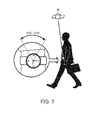
- the direction of maximum radiation of the antenna faces the zenith when the user's arm on which the electronic timepiece with internal antenna is worn is hanging down at the side or in front of the body as shown in FIG. 7 , and sufficiently good reception performance can be obtained with the antenna.
- the antenna according to this embodiment of the invention therefore provides the optimal practical antenna directivity based on the frequent posture of the user when outdoors.
- the antenna has an annular dielectric
- the circumference length of the antenna can be shortened using the wavelength shortening effect of the dielectric, and the size of the antenna can therefore be reduced.
- the length of the driven element disposed to the dielectric can be set appropriately.
- the impedance of the antenna and the circuit electrically connected to the antenna can therefore be easily matched.
- the invention can reduce the resonance frequency of the antenna and improve the impedance characteristic. Return loss at the resonance frequency can therefore be reduced, and the reception performance of the antenna to the radio signals to be received can be increased, by matching the resonance frequency of the antenna to the signals to be received.
- the invention can therefore reduce the size of the antenna while maintaining sufficient reception performance.
- Annular means a shape like an endless ring with no break therein, and the shape of the ring could be round, oval, rectangular, or other polygon.
- the time display unit may indicate the time by rotating hands 13 (13a - 13c) on a center pivot 12 over a dial 11, or have an LCD panel with a display area of a size equal to the dial 11 and display the time by displaying an image of a dial 11 and hands 13 in the display area, or display time digitally on an LCD panel 15 as shown in FIG. 16 , for example.
- Disposed to or on the dielectric is also not limited to being disposed on the surface of the dielectric, and includes being embedded in the dielectric. More specifically, the driven element and parasitic element may be formed on the surface of the dielectric by plating or a silver paste printing process ( FIG. 5 , FIG. 10 , FIG. 13 , FIG. 15 ), or embedded in the dielectric ( FIG. 11 ) by insert molding, for example.
- the driven element is disposed on the inside of the parasitic element relative to the center axis of the dielectric.
- part of the side of the case (case 80) maybemade frommetal or other conductive material. Because the area near the antenna has high current density and is sensitive to external factors, the reception performance of the antenna becomes unstable when the case 80 is touched with a finger. However, by disposing the driven element on the inside of the parasitic element, the distance from the side of the case (case 80) to the driven element canbe increased compared with a configuration having the driven element on the outside of the parasitic element, and the reception performance of the antenna can be stabilized.
- the dielectric has a flat top surface, and a slope formed from the top surface so that the height to the time display unit decreases to the inside; and the driven element is disposed on the slope.
- This aspect of the invention can increase the distance from the side of the outside case (case 80) to the driven element, and can therefore stabilize the reception performance of the antenna. Furthermore, because the height to the time display unit decreases as the slope goes to the inside, the time display unit can be read from a wide angle direction. Furthermore, because the driven element is disposed to this slope, radio waves can be received from a wide range of angles, and good reception performance can be assured in the antenna.
- An electronic timepiece with internal antenna preferably also has a circuit board that is housed in the case and has a reception circuit disposed thereto; and a coil spring that is housed in the case, disposed at the feed position, and feeds a specific potential to the driven element.
- One end of the coil spring is electrically connected to the driven element, the other end is electrically connected to the circuit board and is fed with the specific potential.
- the side part not including both ends is surrounded by a cylindrical conductive member to which ground potential is supplied.
- the coil spring When the specific potential is supplied to the driven element using a coil spring, the coil spring is electrically connected to the driven element and at the same potential as the driven element, and therefore functions as part of the loop antenna.
- the coil spring produces a magnetic field when current flows, and picks up noise produced by the circuit elements and the stepper motor inside the electronic timepiece, the reception performance of the antenna drops due to the effects of this magnetic field and noise.
- this aspect of the invention surrounds the side part of the coil spring with a cylindrical conductive member to which the ground potential is supplied, and the cylindrical conductive member functions as a magnetic shield. Change in the current density near the antenna caused by the magnetic field produced by the coil spring, and the coil spring picking up noise from circuits and the stepper motor inside the electronic timepiece, are therefore suppressed, and good reception performance can be maintained in the antenna.
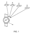
- FIG. 1 shows the configuration of a time adjustment system using the GPS system.
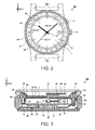
- FIG. 2 is a plan view of an electronic timepiece.
- FIG. 3 is a section view showing main parts of the electronic timepiece.
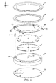
- FIG. 4 is an exploded oblique view of main parts of the electronic timepiece.
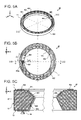
- FIG. 5A to FIG. 5C describe the structure of the antenna.
- FIG. 6 is a graph showing the radiation pattern in the x-y plane of the antenna.
- FIG. 7 shows wearing the electronic timepiece outdoors.
- FIG. 8 shows the range in which the feed position is located.
- FIG. 9 is a block diagram showing the circuits of the electronic timepiece.
- FIG. 10 is a section view of the antenna in variation 2 of the preferred embodiment.
- FIG. 11 is a section view of the antenna in variation 3 of the preferred embodiment.
- FIG. 12 is a section view of the antenna in variation 4 of the preferred embodiment.
- FIG. 13 is a section view of the antenna in variation 5 of the preferred embodiment.
- FIG. 14 is a section view of the feed pin in variation 6 of the preferred embodiment.
- FIG. 15 is a section view of the antenna in variation 8 of the preferred embodiment.
- FIG. 16 is aplanviewof the electronic timepiece in variation 10 of the preferred embodiment.
- FIG. 1 shows the general configuration of a time adjustment system using the GPS system.
- the electronic timepiece 100 is a wristwatch that receives signals (radio signals) from GPS satellites 20 and adjusts the time based thereon, and displays the time on the surface (side) (referred to below as the “face") on the opposite side as the surface (referred to below as the "back") that contacts the wrist.
- signals radio signals
- Each GPS satellite 20 is on a semi-geosynchronous orbit, and transmits a C/A (Coarse/Acquisition) code and navigation messages superimposed on a 1.57542 GHz RF signal (L1 signal).
- the 1.57542 GHz signal carrying a C/A code and navigation message is referred to herein as simply a "satellite signal.”
- These satellite signals are right-handed circularly polarized waves.
- a C/A code is a 1023-bit pseudorandom noise code unique to a specific GPS satellite 20.
- Each GPS satellite 20 carries an atomic clock, and the highly precise time information (“GPS time information" below) kept by the atomic clock is included in the navigation message as the time that the satellite signalwas transmitted by the GPS satellite 20.
- GPS time information the highly precise time information kept by the atomic clock is included in the navigation message as the time that the satellite signalwas transmitted by the GPS satellite 20.
- the time difference of the atomic clock onboard each GPS satellite 20 is measured by the ground control segment, and a time correction parameter for correcting this time difference is also included in the navigation message.
- Precise orbit information for the GPS satellite 20
- general orbit information for all GPS satellites 20 in the constellation
- UTC offset value indicating the offset between UTC (Coordinated Universal Time) and the GPS time
- an ionospheric correction parameter are also included in the navigation message.
- the GPS satellite 20 After spectrum spreading of the navigation message with the C/A code, the GPS satellite 20 produces a satellite signal by BPSK (binaryphase shift keying) modulation multiplying the spread-spectrum signal with the 1.57542 GHz carrier.
- the electronic timepiece 100 extracts the navigation message from the received satellite signal by reversing the flowof satellite signal generation by the GPS satellite 20 (demodulating the BPSK modulated signal, then spread-spectrum despreading). Because the C/A code used for spectrum spreading is different for each GPS satellite 20, the electronic timepiece 100 can determine from which GPS satellite 20 the signal was received.
- the electronic timepiece 100 can accurately adjust the time kept by the electronic timepiece 100 (below, the "internal time") to the correct current time using the GPS time information and time correction parameter contained in the satellite signals received from a single GPS satellite 20.
- the electronic timepiece 100 can also acquire positioning information (location information such as the latitude and longitude) indicating the current location of the electronic timepiece 100 by receiving satellite signals from at least three (normally four) or more GPS satellites 20 and extracting the GPS time information and orbit information (ephemeris) of each GPS satellite 20 contained in the received signals.
- the acquired positioning information can also be used to adjust the time zone.
- the electronic timepiece 100 also calculates the distance to each GPS satellite 20 from the difference between the time that the satellite signal was received (arrival time) and the transmission time contained in the satellite signal, and calculates the current location of the electronic timepiece 100 by triangulation based on the distance to three ormore GPS satellites 20.
- the electronic timepiece 100 uses a crystal oscillator, and cannot keep time as precisely as an atomic clock. A time error as short as one-millionth of a second results in a distance error of approximately 300 meters. As a result, the electronic timepiece 100 normally receives satellite signals from four or more GPS satellites 20 to correct the internal time while acquiring positioning information.
- FIG. 2 is a plan view of the electronic timepiece 100.
- the electronic timepiece 100 has a cylindrical outside case 80 made of metal or other conductive material.
- An annular bezel 81 made of a non-conductive material such as ceramic or plastic is fit to the top (face side) of the case 80, and the opening in the bezel 81 is covered by a transparent crystal 84.
- Conductive lugs 80a formed in unison with the case 80 are disposed to the case 80 at two locations, at the top and the bottom as seen in the figure.
- a wristband for holding the electronic timepiece 100 on the wrist is attached to the lugs 80a.
- An annular dial ring 83 made of a non-conductive material such as ceramic or plastic is disposed inside the bezel 81, and a round dial 11 is disposed inside the dial ring 83.
- Bar-shaped hour markers are disposed every 30 degrees around the dial ring 83, and part of each hour marker protrudes above the top of the dial 11. Additional minute markers are also inscribed every 6 degrees between adjacent hour markers.
- the markers could alternatively be disposed on the dial 11, and the numbers 1 to 12 could be used instead of the bar-shaped hour markers.
- the appearance of the dial ring 83 and the dial 11 are thus not limited to the appearance shown in the figure.
- Hands 13 (second hand 13a, minute hand 13b, and hour hand 13c) that turn on a center pivot 12 and indicate the time, for example, are disposed above the dial 11.
- the user can see the dial ring 83, dial 11, and hands 13 through the crystal 84.
- An annular antenna 40 is disposed below (on the back side of) the dial ring 83.
- the electronic timepiece 100 also has a crown 16 and pushers 17, 18.
- the crown 16 is at the 3:00 position, one pusher 17 is at the 2:00 position, and the other pusher 18 is at the 4:00 position.
- the time information acquisition mode is an operating mode for receiving satellite signals and acquiring the GPS time information and time correction parameter from at least one GPS satellite 20, and adjusting the internal time to the correct time.
- the positioning information acquisition mode is an operating mode for receiving satellite signals fromat least three GPS satellites 20 to acquire the current location of the electronic timepiece 100 and adjust the internal time to the correct time reflecting the local time zone.
- the electronic timepiece 100 can also regularly automatically execute the time information acquisition mode and the positioning information acquisition mode.
- the internal structure of the electronic timepiece 100 is described next.
- FIG. 3 is a section view showing main parts of the electronic timepiece 100
- FIG. 4 is an exploded oblique view showing parts of the electronic timepiece 100.
- the annular bezel 81 is fit to the top (face side) of the cylindrical case 80, and the top opening of the bezel 81 is covered by the round crystal 84.
- the opening on the bottom (back side) of the case 80 is covered by a back cover 85 made of stainless steel, titanium, or other conductive material.
- the case 80 and back cover 85 screw together, for example.
- the outside case of the electronic timepiece 100 thus includes the case 80, bezel 81, crystal 84, and back cover 85.
- the annular dial ring 83 is disposed to the inside circumference of the bezel 81 below the crystal 84.
- the outside circumference side of the dial ring 83 is flat and contacts the inside surface of the bezel 81, and the inside circumference side is bevelled and slopes to the inside.
- a donut-shaped storage space is formed below the dial ring 83, and the annular antenna 40 is housed in this space.
- the antenna 40 is disposed on the inside side of the inside circumference of the case 80 and bezel 81, and the top of the antenna 40 is covered by the dial ring 83.
- An annular ground plane 90 made of metal or other conductive material is disposed below the antenna 40. As shown in FIG. 4 , four holes are formed in the ground plane 90 in addition to a through-hole 90b for the feed pin 44, and a conductive pin 93 as shown in FIG. 3 is disposed in each of these four holes. Four holes for passing conductive pins 93 are also formed in the main plate 38 and the edge of the circuit board 25 matching the holes in the ground plane 90. See FIG. 4 .
- the ground potential of the circuit block including a GPS reception unit 26 and control unit 70 is supplied through the circuit board 25 to the conductive pins 93, and the ground potential of the four conductive pins 93 is supplied to the ground plane 90.
- Four conductive springs 90a are also disposed to the ground plane 90 as shown in FIG. 4 . Part of each conductive spring 90a contacts the inside surface of the case 80 with the urging force of the spring (see FIG. 3 ), and the conductive springs 90a are thereby electrically connected to the case 80. The ground potential is therefore also supplied through the ground plane 90 (conductive springs 90a) to the case 80.
- the dial 11 and solar panel 87 are disposed inside the antenna 40.
- the dial 11 is made of plastic or other optically transparent non-conductive material.
- the solar panel 87 is a round disc having plural solar cells (photovoltaic devices) that convert light energy to electrical energy (power) connected in series.
- the dial 11 and solar panel 87 are superimposed with each other and have a center hole through which the center pivot 12 passes.
- the main plate 38 made of plastic, ceramic, or other non-conductive material is disposed below the solar panel 87.
- the center pivot 12 extends through the solar panel 87 and main plate 38 in the thickness direction between the face and back.
- the center pivot 12 is the center of the electronic timepiece 100 when the electronic timepiece 100 is seen from the direction perpendicular to the dial 11 (that is, when the electronic timepiece 100 is seen in plan view).
- the hands 13 (13a to 13c) are disposed between the crystal 84 and the dial 11 inside the inside circumference of the antenna 40 as shown in FIG. 3 .
- a drive mechanism 30 that causes the center pivot 12 to turn and drives the hands 13 is disposed below the main plate 38 as shown in FIG. 3 .
- the drive mechanism 30 includes a stepper motor M and wheel train, and drives the hands 13 by the stepper motor M causing the center pivot 12 to turn through the wheel train.
- the hour hand 13c turns one revolution in 12 hours
- the minute hand 13b turns one revolution in 60 minutes
- the second hand 13a turns one revolution in 60 seconds.
- the time display unit includes, for example, the dial 11, center pivot 12, hands 13 (13a to 13c), and the drive mechanism 30.
- the circuit board 25 is disposed below the main plate 38 and drive mechanism 30.
- a circuit block including a GPS reception unit 26 and control unit 70 is disposed on the bottom (on the surface facing the back of the wristwatch) of the circuit board 25.
- the GPS reception unit 26 is a single-chip IC module, for example, and includes analog and digital circuits.
- the control unit 70 controls the operation of the GPS reception unit 26 and drive mechanism 30.
- a storage battery 27 is disposed on the bottom of the circuit board 25 ( FIG. 3 ).
- the storage battery 27 in this embodiment is a lithium ion battery, and is charged by the power produced by the solar panel 87.
- the GPS reception unit 26 and control unit 70 are covered by a shield 91 made of metal or other conductive material as shown in FIG. 3 .
- the ground potential is supplied to the shield 91, and the ground potential is further supplied through the shield 91 and a metal circuit support 39 to the back cover 85 and case 80.
- the ground potential is also supplied through the circuit board 25 and conductive pins 93 to the ground plane 90 and case 80.
- the members constituting the ground potential supply path (such as the shield 91, circuit support 39, back cover 85, conductive pin 93, ground plane 90, and conductive springs 90a) are processed with gold plating or anticorrosion coating on the contact surfaces between the members.
- the conductive pins 93 are screwed tight. Contact resistance between the members of the ground potential supply path can therefore be held as low as possible for a long time.
- the feed pin 44 is a pin connector made of metal or other conductive material, and has an internal coil spring. As shown in FIG. 4 , the feed pin 44 is electrically connected through through-holes 38a, 90b in the main plate 38 and ground plane 90 to the top of the circuit board 25 and the bottom of the antenna 40. The top end of the feed pin 44 contacts the bottom of the antenna 40 (more specifically, the feed part 404 described below) due to the urging force of the coil spring. The bottom of the feed pin 44 likewise contacts the top of the circuit board 25 (more specifically, the part where the wiring pattern supplying a specific potential is formed) due to the urging force of the coil spring. A specific potential is fed to the antenna 40 through the feed pin 44.
- FIG. 5A to FIG. 5C describe the construction of the antenna 40.
- FIG. 5A is an oblique view of the antenna 40
- FIG. 5B is a plan view of the antenna 40
- FIG. 5C is a section view of the antenna 40 through line G-g in FIG. 5B .
- the antenna 40 includes an annular base 401 made of plastic, ceramic, or other dielectric material, a parasitic element 402 formed on the surface of the base 401, a driven element 403, and a feed part 404.
- the parasitic element 402, driven element 403, and feed part 404 are each made of metal or other conductive material, and can be formed by a plating or silver paste printing process.
- the dielectric constant of the base 401 material can be adjusted to approximately 5 - 20 by mixing a dielectric material that is used in high frequency applications, such as titanium oxide, with resin.
- the base 401 has a pentagonal section including a top T1, outside face T2, bottom T3, slope TP1, and slope TP2.
- the parasitic element 402 is formed on the top T1, and the driven element 403 is formed on slope TP1.
- the feed part 404 is formed on the slope TP1, slope TP2, and bottom T3.
- the end of the feed part 404 on the slope TP1 side connects to the driven element 403, and the top of the feed pin 44 contacts the end of the feed part 404 on the bottom T3.
- a specific potential is therefore supplied through the feed pin 44 and feed part 404 to the driven element 403. Potential from an external source is not supplied to the parasitic element 402.
- the parasitic element 402 is annular, that is, is formed in an endless O-shape.
- the driven element 403, however, has a notch 405, and is therefore C-shaped with part of the ring missing.
- the feed part 404 is connected to an end of the C-shaped driven element 403. As shown in FIG. 5B , the part (end) of the driven element 403 to which the feed part 404 is connected is a feed position 403a to which a specific potential is supplied.
- the feed position 403a is disposed at approximately 9:00 on the electronic timepiece 100. More specifically, when the electronic timepiece 100 is seen in plan view, the feed position 403a, feed part 404, and feed pin 44 are disposed at approximately 9:00 relative to the center (center pivot 12) of the electronic timepiece 100.
- the parasitic element 402 and driven element 403 are disposed with a specific gap therebetween, and when current flows to the driven element 403, current is induced in the parasitic element 402. That is, the distance between the parasitic element 402 and driven element 403 is a distance enabling electromagnetic coupling therebetween.
- the driven element 403 and parasitic element 402 therefore couple electromagnetically, and together function as an antenna element that converts electromagnetic waves to current. Because the parasitic element 402 is O-shaped, the antenna 40 overall functions as an O-shaped loop antenna.
- the driven element 403 to which a specific potential is supplied and the ground plane 90 to which ground potential is supplied therefore resonate, and the electronic timepiece 100 can receive radio waves (satellite signals) from a GPS satellite 20 by this resonation.
- GPS satellites 20 transmit satellite signals at 1.575 GHz, the length of one wave is approximately 19 cm. Because an antenna length of approximately 1.0 - 1.2 wavelength is required to receive circularly polarized waves, a loop antenna of approximately 19 - 24 cm is required to receive a GPS signal. Rendering a loop antenna with this antenna length in a wristwatch, however, results in a large wristwatch.
- the resonance frequency of the antenna 40 can also be reduced and the impedance characteristic can be improved by electromagnetically coupling the parasitic element 402 to the driven element 403. Return loss at the resonance frequency can therefore be reduced, and the satellite signal reception performance of the antenna 40 can be increased by adjusting the resonance frequency of the antenna 40 to the satellite signal.
- contact resistance can be kept low for a long time and a drop in the receptionperformance of the antenna 40 can be prevented by also applying gold plating or anticorrosion coating process to the contact surfaces of the feed pin 44 and feed part 404, and the contact surfaces of the feed pin 44 and circuit board 25.
- FIG. 6 is a graph showing the radiation pattern in the x-y plane of the antenna 40.
- the x-axis is the direction from the center (center pivot 12) to 3:00 when the electronic timepiece 100 is seen inplanview. They-axis is the direction from the center to 12:00 when the electronic timepiece 100 is seen inplanview.
- the feedposition 403a is disposed in the direction of 9:00 from the center when the electronic timepiece 100 is seen in plan view.
- the direction of maximum radiation in the x-y plane of the antenna 40 substantially matches this as shown in FIG. 6 . More specifically, the direction of maximum radiation in the x-y plane of the antenna 40 is in the direction between 8:00 and 9:00, and the opposite direction, as shown in FIG. 6 .
- the electronic timepiece 100 receives satellite signals when the user is outdoors, but when the user is outdoors, the arm on which the electronic timepiece 100 is worn is often hanging down at the side as shown in FIG. 7 or in front of the body. In this posture, the direction from the center to 9:00 on the electronic timepiece 100 is pointing generally toward the zenith as shown in FIG. 7 .
- the probability that the direction of maximum radiation of the antenna 40 is towards the zenith when the user is outdoors can therefore be increased by disposing the feed position 403a (the location of the feed part 404 and feed pin 44) in the vicinity of 9:00 from the center of the electronic timepiece 100.
- feed pin 44 and feed part 404 are electrically connected to the driven element 403 and the same potential as the driven element 403, they function as part of the loop antenna.
- the crown 16 and pushers 17, 18 are also disposed in the area from 2:00 to 4:00 of the electronic timepiece 100 as shown in FIG. 2 .
- the crown 16 and pushers 17, 18 are made of metal or other conductive material.
- the crown stem (not shown in the figure), which is made of metal or other conductive material, also extends from the crown 16 through the case 80 toward the center of the electronic timepiece 100.
- Stems (not shown in the figure) made of metal or other conductive material also extend from the pushers 17, 18 through the case 80 toward the center of the electronic timepiece 100.
- feed pin 44 and feed part 404 are disposed near the crown 16, pushers 17, 18, and stems thereof ("operating members" below), resonance occurs because these members are all made of conductive materials, the current density near the antenna 40 will change, and the reception performance of the antenna 40 will drop.
- the feed pin 44 and feed part 404 must therefore be disposed near the operating members in order to maintain good reception performance in the antenna 40.
- the antenna 40 receives satellite signals by resonating with the ground plane 90, but conductive members other than the ground plane 90 that are near the antenna 40 include the case 80, and the antenna 40 also resonates with the case 80.
- lugs 80a made of a conductive material are disposed to the part of the case 80 from 11:00 to 1:00 and the part from 5:00 to 7:00. These parts protrude further to the outside and the volume is significantly greater than other parts. If the feed pin 44 and feed part 404 are disposed near the lugs 80a, the reception performance of the antenna 40 drops due to loss from the lugs 80a.
- the feed pin 44 and feed part 404 must not be disposed near the lugs 80a. Tests demonstrated that when the lugs 80a are disposed to the part of the case 80 from 11:00 to 1:00 and the part from 5:00 to 7:00 as shown in FIG. 2 , the reception performance of the antenna 40 can be sufficiently maintained if the feed pin 44 and feed part 404 are disposed in the area from 2:00 to 4:00 or the area from 8:00 to 10:00.
- the feed position 403a (the location of the feed part 404 and feed pin 44) must be in the angular range from approximately 2:00 to approximately 4:00 or the range from approximately 8:00 to approximately 10:00 relative to the center of the electronic timepiece 100.
- the feed position 403a must be in the angular range from approximately 8: 00 to approximately 10: 00 from the center (center pivot 12) of the electronic timepiece 100 as shown in FIG. 8 in order to increase the probability that the direction of maximum radiation of the antenna 40 will be toward the zenith when the user is outdoors and maintain good reception performance in the antenna 40 considering both the operating members and lugs 80a.
- the location of the feed pin 44 and feed part 404 is therefore not limited to approximately 9: 00 from the center of the electronic timepiece 100, and can be in the range from approximately 8: 00 to approximately 10: 00.
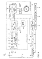
- FIG. 9 is a block diagram showing the circuit configuration of the electronic timepiece 100.
- the electronic timepiece 100 includes a GPS reception unit 26 and a control display unit 36.
- the GPS reception unit 26 executes processes related to receiving satellite signals, locking onto GPS satellites20,generating positioninginformation,and generatingtime adjustment information, for example.
- the control display unit 36 executes processes including keeping and adjusting the internal time, and movement of the hands 13.
- a solar panel 87 charges the storage battery 27 through the charging control circuit 29.
- the storage battery 27 supplies drive power through a regulator 34 to the control displayunit 36, and supplies drive power through another regulator 35 to the GPS reception unit 26.
- a voltage detection circuit 37 detects the voltage of the storage battery 27 and outputs to a control unit 70.
- Regulator 35 could be split into a regulator that supplies drive power to the RF (radio frequency) unit 50, and a regulator that supplies drive power to a baseband unit 60.
- the regulator that supplies power to the RF unit 50 could be disposed in the RF unit 50.
- Aratedpotential generator 33 generates a specificpotential with a predetermined potential difference to the ground pot.
- the specific potential generated by the rated potential generator 33 is supplied through the circuit board 25 and feed pin 44 to the antenna 40 (driven element 403).
- the antenna40 receivessatellitesignalsfrom GPSsatellites 20.
- a SAW (surface acoustic wave) filter 32 is disposed after the antenna 40.
- the SAW filter 32 functions as a bandpass filter that passes signals in the 1.5 GHz waveband, and extracts the satellite signal from the signals received by the antenna 40.
- the GPS receptionunit 26 includes the RF unit 50 and baseband unit 60.
- the RF unit 50 includes a LNA (low noise amplifier) 51, mixer 52, VCO (voltage controlled oscillator) 53, PLL (phase-locked loop) circuit 54, IF (intermediate frequency) amplifier 55, IF filter 56, and A/D converter 57.
- LNA low noise amplifier
- VCO voltage controlled oscillator
- PLL phase-locked loop
- Signals (satellite signals) passed by the SAW filter 32 are input to the RF unit 50 and amplified by the LNA 51.
- the satellite signal amplified by the LNA 51 is mixed by the mixer 52 with the clock signal output by the VCO 53, and down-converted to a signal in the intermediate frequency band.
- the PLL circuit 54 phase compares a clock signal obtained by frequency dividing the output clock signal of the VCO 53 with a reference clock signal supplied from the baseband unit 60, and synchronizes the output clock signal of the VCO 53 to the reference clock signal.
- the VCO 53 can output a stable clock signal with high frequency precision. Note that several megahertz, for example, can be selected as the intermediate frequency.
- the signal in the IF band output from the mixer 52 is amplified by the IF amplifier 55.
- the IF amplifier 55 amplifies both the IF signal and the high frequency component of several GHz.
- the IF filter 56 extracts the IF signal and removes the high frequency component (more accurately, attenuates the signal to a specific level or less).
- the IF signal passed by the IF filter 56 is converted to a digital signal by the A/D converter 57.
- the baseband unit 60 includes, for example, a DSP (digital signal processor) 61, CPU (central processing unit) 62, SRAM (static random access memory) 63, and RTC (real-time clock) 64.
- DSP digital signal processor
- CPU central processing unit
- SRAM static random access memory
- RTC real-time clock
- a TCXO (temperature compensated crystal oscillator) 65 and flash memory 66 are also connected to the baseband unit 60.
- the TCXO 65 generates a reference clock signal of a substantially constant frequency regardless of temperature. Operation of the baseband unit 60 is synchronized to the reference clock signal output by the TCXO 65.
- the RTC 64 generates the timing for satellite signal processing, and counts up at the reference clock signal output from the TCXO 65.
- Time zone information for example, is stored in flashmemory 66.
- the time zone information defines the time difference to UTC related to known coordinates (such as latitude and longitude).
- the baseband unit 60 executes a process that demodulates the baseband signal from the digital signal (IF signal) output from the A/D converter 57 of the RF unit 50 when the time information acquisition mode or the positioning information acquisition mode is set.
- the baseband unit 60 executes a process that generates a local code of the same pattern as each C/A code, and correlates the local codes to the C/Acode contained in the baseband signal, in the satellite search step.
- the baseband unit 60 adjusts the timing when the local code is generated to find the peak correlation to each local code, and when the correlation equals or exceeds a threshold value, determines that the local code synchronized with the GPS satellite 20 (that is, locked onto a GPS satellite 20).
- the GPS system uses a CDMA (Code Division Multiple Access) method whereby all GPS satellites 20 transmit satellite signals on the same frequency using different C/A codes. The GPS satellites 20 that can be locked onto can therefore be found by identifying the C/A code contained in the received satellite signal.
- CDMA Code Division Multiple Access
- the baseband unit 60 To acquire the navigation message from the satellite signal of the GPS satellite 20 that was locked onto, the baseband unit 60 also executes a process that mixes the baseband signal with the local code of the same pattern as the C/A code of the GPS satellite 20 that was locked. The navigation message from the GPS satellite 20 that was locked onto is thereby demodulated. The baseband unit 60 then executes a process to detect the TLM word (preamble data) of each subframe in the navigation message, and acquire and store in SRAM 63 satellite information such as the orbit information and GPS time information contained in each subframe.
- the GPS time information as used here is the week number (WN) and Z count, but the Z count data alone could be acquired if the week number was previously acquired.
- the baseband unit 60 then generates the time adjustment information based on the satellite information.
- the time adjustment information is information for correcting the internal time kept by the electronic timepiece 100.
- the baseband unit 60 can generate the time adjustment information using the GPS time information, time adjustment parameter, or UTC offset contained in the satellite information from one GPS satellite 20, for example.
- the baseband unit 60 can also generate the time adjustment information from satellite information from a plurality of GPS satellites 20.
- the time adjustment information in the time information acquisition mode could be, for example, the GPS time information itself, the GPS time information after being corrected based on the time adjustment parameter, or time information acquired by adding the time adjustment parameter or UTC offset to the GPS time information. Further alternatively, information indicating the difference between this time information and the internal time of the electronic timepiece 100 could be used as the time adjustment information.
- the baseband unit 60 receives satellite information from at least three (and normally four) or more GPS satellites 20, and acquires the location of the electronic timepiece 100 using the received satellite information.
- the baseband unit 60 references the time difference information stored in flash memory 66, and acquires the time difference at the acquired location.
- the baseband unit 60 then adds the acquired time difference to the time adjustment information generated using the same method used in the time information acquisition mode.
- the time adjustment information used in the positioning information acquisition mode therefore reflects the time difference at the current location of the electronic timepiece 100.
- the control display unit 36 includes a control unit 70, crystal oscillator 73, and drive circuit 74.
- the control unit 70 can be rendered by a configuration including a storage unit 71 and a CPU with a RTC (real-time clock) 72.
- the control unit 70 outputs control signals to the GPS reception unit 26, and controls operation of the GPS reception unit 26.
- the control unit 70 also controls movement of the hands 13 (13a to 13c) through the drive circuit 74.
- the control unit 70 also controls operation of regulators 34, 35 and the rated potential generator 33 based on output from the voltage detection circuit 37.
- the time adjustment information and positioning information output from the GPS reception unit 26 are stored in the storage unit 71.
- the RTC 72 keeps the internal time.
- the RTC 72 operates continuously, and counts up at the reference clock signal generated by the crystal oscillator 73.
- the control unit 70 can therefore continue moving the hands 13 based on the internal time kept by the RTC 72 whether the time information acquisition mode or the positioning information acquisition mode is set.
- the control unit 70 corrects the internal time kept by the RTC 72 according to the time adjustment information.
- the control unit 70 also drives the hands 13 through the drive circuit 74 so that the hands 13 (13a to 13c) indicate the internal time after being corrected.
- the internal time of the electronic timepiece 100 is set to the correct time.
- the internal time can also be adjusted to the correct time reflecting the time difference (time zone) at the current location of the electronic timepiece 100.
- this embodiment of the invention has a C-shaped driven element 403 to which a specific potential is supplied and an O-shaped parasitic element 402 disposed in parallel with a specific gap therebetween on an annular base 401 (dielectric) forming the body of the antenna 40.
- the driven element 403 and parasitic element 402 electromagnetically couple, and together function as an antenna element that converts electromagnetic waves to current.
- the antenna 40 overall functions as an O-shaped loop antenna.
- the radiant directivity in the loop plane (x-y plane) of this loop antenna is greatest in or near the direction of the feed position 403a (where the feed pin 44 and feed part 404 are disposed) from the center of the loop.
- the direction of maximum radiation of the antenna 40 faces the zenith when the user's arm on which the electronic timepiece 100 is worn is hanging down at the side or in front of the body as shown in FIG. 7 , and sufficiently good reception performance can be obtained with the antenna 40.
- the antenna according to this embodiment of the invention therefore provides the optimal practical antenna directivity based on the frequent posture of the user when outdoors.
- the antenna 40 has an annular base 401 (dielectric)
- the circumference length of the antenna 40 can be shortened using the wavelength shortening effect of the dielectric, and the size of the antenna 40 can therefore be reduced.
- this embodiment of the invention can also reduce the resonance frequency of the antenna 40 and improve the impedance characteristic. Return loss at the resonance frequency can therefore be reduced, and the satellite signal reception performance of the antenna 40 can be increased by tuning the resonance frequency of the antenna 40 to the satellite signal.
- the invention thus enables reducing the size of the antenna 40 while maintaining sufficient reception performance.
- the driven element 403 is disposed on the inside of the parasitic element 402 in this embodiment relative to the center axis of the the base 401 of the antenna 40 ( FIG. 5B ). Because the area near the antenna 40 has high current density and is sensitive to external factors, the reception performance of the antenna 40 becomes unstable when the case 80 is touched with a finger if the case 80 member rendering the side of the outside case is made of metal or other conductive material.
- the driven element 403 By disposing the driven element 403 on the inside of the parasitic element 402, the distance from the case 80 to the driven element 403 can be increased compared with a configuration having the driven element 403 on the outside of the parasitic element 402, and the reception performance of the antenna 40 can be stabilized.
- the annular base 401 of the antenna 40 in this embodiment has a flat top T1 located on the outside circumference side, a slope TP1 that is located on the inside circumference side and formed so that the height to the dial 11 decreases as the slope TP1 descends to the inside, and the driven element 403 is disposed to this slope TP1. Because the distance from the case 80 to the driven element 403 can be increased with this configuration, the reception performance of the antenna 40 can be stabilized.
- the dial 11 can be read from a wide angle direction. Furthermore, because the range of angles from which radio waves can be received is increased by disposing the driven element 403 to this slope TP1, good reception performance can be assured in the antenna 40. Providing this slope TP1 also makes the electronic timepiece 100 appear thinner, and improves the appearance.
- the invention is not limited to the foregoing embodiment, and can be varied in many ways such as described in the following variations. Two or more of the variations described below can also be desirably combined.
- the parasitic element 402 is not limited to an endless O-shape, and like the driven element 403 can be C-shaped with a notch. In this variation the entire antenna 40 functions as a C-shaped loop antenna.
- the feed position 403a in the antenna 40 shown in FIG. 5 is not limited to an end of the driven element 403, and can be disposed to a part of the driven element 403 other than an end.
- the length of the driven element 403 in the foregoing embodiment is set to resonate to the satellite signal, but the length of the parasitic element 402 can be set to resonate to the satellite signal.
- the impedance between the antenna 40 and the circuit (the circuit block including the GPS reception unit 26 and control unit 70) electrically connected to the antenna 40 can be easilymatched.
- FIG. 10 is a section view of the antenna in variation 2, and is the same as the view in FIG. 5C .
- the base 411 of the antenna in this variation does not have a slope TP2, and slope TP1 continues to the bottom T3.
- the top T1 of the base 411 is smaller and the slope TP1 is larger than the configuration shown in FIG. 5C .
- the parasitic element 402 is formed in addition to the driven element 403 on the slope TP1, and nothing is disposed to the top T1. Both the driven element 403 and parasitic element 402 can thus be disposed to slope TP1.
- FIG. 11 is a section view of the antenna in variation 3, and is the same as the view in FIG. 5C .
- the base 421 of the antenna in this variation has a vertical inside face T4 instead of a slope TP2. All of the parasitic element 412 and the driven element 413, and part of the feed part 424, are embedded in the base 421.
- This configuration can be manufactured by insert molding. Insert molding enables manufacturing the antenna at a lower cost thanwhen the parasitic element 402, driven element 403, and feed part 404 are formed on the surface of the base 401 as shown in FIG. 5C by a plating or silver paste printing process.
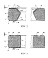
- FIG. 12 is a section view of the antenna in variation 4, and is the same as the view in FIG. 5C .
- the parasitic element 402 and driven element 403 are affixed to the base 401 by flexible tape 500.
- This configuration can be manufactured, for example, by forming the parasitic element 402 and driven element 403 on flexible tape 500, and affixing the flexible tape 500 to the surface of the base 401 (top T1 and slope TP1).
- This manufacturing method enables manufacturing the antenna at a lower cost thanwhen the parasitic element 402 and driven element 403 are formed directly on the surface of the base 401 by a plating or silver paste printing process.
- the feed part 404 can also be affixed to the base 401 using the flexible tape 500.
- FIG. 13 is a section view of the antenna in variation 5, and is the same as the view in FIG. 5C .
- the base 431 of the antenna in this variation is a rectangle in section with a top T12, outside face T12, bottom T13, and inside face T14.
- the parasitic element 402 and driven element 403 are formed on the top T11.
- the feed part 434 is formed on the top T11, inside face T14, and bottom T13.
- the base 431 in this configuration does not need to have a slope TP1.
- the locations of the parasitic element 402 and driven element 403 can also be reversed. More specifically, the driven element 403 can be on the outside of the parasitic element 402.
- the feed part 434 is formed on the top T11, outside face T12, and bottom T13. If the feed part 434 is thus formed on the outside face T12, the case 80 is preferably made of a plastic, ceramic, or other non-conductive material.
- the feed pin 44 and driven element 403 are electrically connected and at the same potential as the driven element 403, and therefore function as part of the loop antenna. Because the coil spring inside the feed pin 44 produces a magnetic field when current flows, and also picks up noise produced by the circuit elements and stepper motor M inside the electronic timepiece 100, reception performance of the antenna 40 drops due to the effects of this magnetic field and noise. To avoid this, the feed pin 44 can be configured as described below.
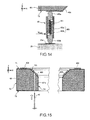
- FIG. 14 is a section view of main parts of a feed pin 45 according to variation 6.
- the feed pin 45 in this embodiment has a coil spring 451 made of metal or other conductive material.
- a contact 452a, 452b made of metal or other conductive material is connected to each end of the coil spring 451.
- One contact 452a contacts the feed part 404 formed on the bottom T3 of the base 401 due to the urging force of the coil spring 451, and connects electrically to the feed part 404.
- the other contact 452b contacts the wiring pattern 25a formed on the top of the circuit board 25 due to the urging force of the coil spring 451, and connects electrically to the wiring pattern 25a.
- a specific potential that feeds the driven element 403 is supplied to the wiring pattern 25a.
- the feed pin 45 also has a cylindrical shield case 453.
- the shield case 453 includes an outside wall 453a made of metal or other conductive material, and an inside wall 453b made of plastic, ceramic, or other insulator. Ground potential V GND is supplied to the outside wall 453a.
- the outside wall 453a functions as a magnetic shield.
- the outside wall 453a therefore suppresses change in the current density near the antenna 40 caused by the magnetic field produced by the coil spring 451, and the coil spring 451 picking up noise from circuits and the stepper motor M inside the electronic timepiece 100, and enables maintaining good reception performance in the antenna 40.
- a leaf spring, lead, coaxial cable, or flexible printed circuit can be used to electrically connect the feed part 404 of the antenna 40 and the circuit board 25, and supply a specific potential.
- FIG. 15 is a section view of the antenna in variation 8, and is the same as the view in FIG. 5C .
- the antenna in this variation differs from the antenna 40 shown in FIG. 5 in that (1) the base 421 has a vertical inside face T4 instead of slope TP2, (2) there is no feed part 404, and (3) a hole 421a is formed from the slope TP1 to the bottom T3 of the base 421. Note that there is only one hole 421a, and similarly to the feed position 403a described above, the hole 421a is formed in the direction of approximately 8:00 to approximately 10:00 from the center (center pivot 12) of the electronic timepiece 100 in plan view.
- a rod-shaped feed pin 46 is used instead of the feed pin 44 described above.
- This feed pin 46 is made of metal or other conductive material, one end is inserted to the hole 421a, and the distal end thereof is connected to the driven element 403. The other end of the feed pin 46 is connected to the wiring pattern on the circuit board 25, and a specific potential is supplied thereto. With this configuration there is no need to form a feed part 404 on the surface of the base 421 (dielectric). Disposing a feed part 404 to the antenna is thus not necessary.
- the second hand 13a can be omitted.
- the time display unit is also not limited to indicating the time by rotating hands 13 over a dial 11, and could have an LCD panel with a display area of a size equal to the dial 11, and display the time by displaying an image of a dial 11 and hands 13 in the display area.
- FIG. 16 is a plan view of an electronic timepiece 200 according to variation 10.
- the electronic timepiece 200 in this variation has a rectangular case in which an annular antenna 41 is housed.
- the shape of the ring (loop) of the antenna 41 is substantially rectangular.
- An LCD panel 15 that displays time digitally is disposed on the inside of the antenna 41. While the shape of the ring differs from the antenna 40 shown in FIG. 5 , the antenna 41 similarly has a base (dielectric), parasitic element, driven element, and feed part, and a specific potential is supplied to the driven element through the feed pin and feed part.
- the feed position (location of the feed pin and feed part) is disposed in the area from approximately 8: 00 to approximately 10:00 relative to the center C of the electronic timepiece 200 when the electronic timepiece 200 is seen in plan view.
- the number of conductive pins 93 and conductive springs 90a are also not limited to four, and there maybe one or more.
- the conductive pins 93 and conductive springs 90a can also be omitted, in which event the driven element 403 resonates with the case 80.
- the side of the case in the foregoing embodiments includes the case 80 and bezel 81, but the side of the case can be manufactured as a single member by molding a plastic, ceramic, orothernon-conductive material.
- a charging method other than solar charging may also be used.
- a charging coil can be used to charge the storage battery with power produced by electromagnetic induction from an external charger.
- a lithium battery or other primary cell can also be used instead of a storage battery 27.
- GNSS Global Navigation Satellite Systems
- EU Galileo
- GLONASS Russian
- Beidou China
- IRNSS Indian
- SBAS Satellite Based Augmentation System
- QZSS Quasi-Zenith Satellite System
- An electronic timepiece 100 according to the invention can thus receive radio signals from manmade satellites other than GPS satellites 20 to adjust the internal time.
Landscapes
- Physics & Mathematics (AREA)
- General Physics & Mathematics (AREA)
- Engineering & Computer Science (AREA)
- Radar, Positioning & Navigation (AREA)
- Remote Sensing (AREA)
- Computer Networks & Wireless Communication (AREA)
- Electric Clocks (AREA)
- Electromechanical Clocks (AREA)
- Details Of Aerials (AREA)
- Support Of Aerials (AREA)
Abstract

Description
- The present invention relates to an electronic timepiece with an internal antenna.
- Japanese Unexamined Patent Appl. Pub.
JP-A-H09-307329 loop antenna 20 formed along the outside circumference below thecrystal 5, and lugs 2 for attaching a wrist band at the 12:00 and 6:00 positions of the case 1. As shown inFIG. 1 ofJP-A-H09-307329 antenna 20 is also disposed near one of the lugs 2, that is, the electrode 21 of theantenna 20 is disposed at 12:00 or 6:00. - Japanese Unexamined Patent Appl. Pub.
JP-A-H09-247006 antenna 11 that functions as a loop antenna in unison with thecase 17 of a wrist-worn receiver. As shown inFIG. 1 ofJP-A-H09-247006 band 41 are formed at two locations on thecase 17, and a feed opening 15 for theantenna 11 is disposed near one set of lugs 21. - Because signals from GPS (Global Positioning System) satellites cannot be received indoors, an electronic wristwatch must receive signals from GPS satellites when the user is outdoors. When outdoors, the arm of the user on which the wristwatch is worn is often hanging down at the side or in front of the user' s body. In this posture, the normal direction of the face of the wristwatch is horizontal. For example, with an annular (O-shaped) loop antenna or a C-shaped loop antenna having part of the ring missing, radiant directivity in the plane including the loop plane is greatest at or near the direction in which the feed electrode is disposed as seen from the center of the ring. Therefore, arm of the user on which the wristwatch is worn hanging down or held in front of the body, sufficient reception performance cannot be achieved with the loop antennae disclosed in
JP-A-H09-307329 JP-A-H09-247006 - An electronic timepiece with internal antenna according to the present invention can maintain sufficient reception performance while reducing the size of the antenna.
- An electronic timepiece with internal antenna according to one aspect of the invention has a case; an annular antenna housed in the case; and a time display unit that is housed in the case and displays time. The antenna includes an annular dielectric; a conductive driven element that is disposed on the dielectric, is ring-shaped with a notch therein, and is fed with a specific potential; andaconductiveparasitic element that is disposed on the dielectric with a gap to the driven element, and is an endless ring or a ring with a notch therein. A feed position to which a specific potential is fed is disposed to the driven element at one place, and the feed position is disposed in an angular range from approximately 8:00 to approximately 10:00 from the center of the electronic timepiece with internal antenna when the electronic timepiece with internal antenna is seen in plan view.
- In this aspect of the invention a conductive driven element that is ring-shaped with a notch therein and is fed with a specific potential, and a conductive parasitic element that is an endless ring or a ring with a notch therein, are disposed on the annular dielectric with a gap therebetween. Because current is also induced in the parasitic element when current flows to the driven element, the driven element and parasitic element couple electromagnetically, and together function as an antenna element that converts electromagnetic waves to current.
- The complete antenna functions as a closed-loop (such as O-shaped) or an open-loop (such as C-shaped) loop antenna. The radiant directivity in the plane including the loop plane of this loop antenna is greatest in or near the direction of the feed position from the center of the loop.
- Therefore, by disposing the feed position in the direction of approximately 8:00 to approximately 10:00 from the center of the electronic timepiece with internal antenna when the electronic timepiece wit internal antenna is seen in plan view, the direction of maximum radiation of the antenna faces the zenith when the user's arm on which the electronic timepiece with internal antenna is worn is hanging down at the side or in front of the body as shown in
FIG. 7 , and sufficiently good reception performance can be obtained with the antenna. The antenna according to this embodiment of the invention therefore provides the optimal practical antenna directivity based on the frequent posture of the user when outdoors. - Furthermore, because the antenna has an annular dielectric, the circumference length of the antenna can be shortened using the wavelength shortening effect of the dielectric, and the size of the antenna can therefore be reduced.
- For example, by setting the length of the parasitic element disposed to the dielectric to resonate to the radio signals to be received, the length of the driven element disposed to the dielectric can be set appropriately. The impedance of the antenna and the circuit electrically connected to the antenna can therefore be easily matched.
- Furthermore, by electromagnetically coupling the parasitic element to the driven element, the invention can reduce the resonance frequency of the antenna and improve the impedance characteristic. Return loss at the resonance frequency can therefore be reduced, and the reception performance of the antenna to the radio signals to be received can be increased, by matching the resonance frequency of the antenna to the signals to be received.
- The invention can therefore reduce the size of the antenna while maintaining sufficient reception performance.
- Annular means a shape like an endless ring with no break therein, and the shape of the ring could be round, oval, rectangular, or other polygon.
- The time display unit may indicate the time by rotating hands 13 (13a - 13c) on a
center pivot 12 over adial 11, or have an LCD panel with a display area of a size equal to thedial 11 and display the time by displaying an image of adial 11 andhands 13 in the display area, or display time digitally on anLCD panel 15 as shown inFIG. 16 , for example. - Disposed to or on the dielectric is also not limited to being disposed on the surface of the dielectric, and includes being embedded in the dielectric. More specifically, the driven element and parasitic element may be formed on the surface of the dielectric by plating or a silver paste printing process (
FIG. 5 ,FIG. 10 ,FIG. 13 ,FIG. 15 ), or embedded in the dielectric (FIG. 11 ) by insert molding, for example. - In an electronic timepiece with internal antenna according to another aspect of the invention, the driven element is disposed on the inside of the parasitic element relative to the center axis of the dielectric.
- For example, as further described below, part of the side of the case (case 80) maybemade frommetal or other conductive material. Because the area near the antenna has high current density and is sensitive to external factors, the reception performance of the antenna becomes unstable when the
case 80 is touched with a finger. However, by disposing the driven element on the inside of the parasitic element, the distance from the side of the case (case 80) to the driven element canbe increased compared with a configuration having the driven element on the outside of the parasitic element, and the reception performance of the antenna can be stabilized. - In an electronic timepiece with internal antenna according to another aspect of the invention, the dielectric has a flat top surface, and a slope formed from the top surface so that the height to the time display unit decreases to the inside; and the driven element is disposed on the slope.
- This aspect of the invention can increase the distance from the side of the outside case (case 80) to the driven element, and can therefore stabilize the reception performance of the antenna. Furthermore, because the height to the time display unit decreases as the slope goes to the inside, the time display unit can be read from a wide angle direction. Furthermore, because the driven element is disposed to this slope, radio waves can be received from a wide range of angles, and good reception performance can be assured in the antenna.
- An electronic timepiece with internal antenna according to another aspect of the invention preferably also has a circuit board that is housed in the case and has a reception circuit disposed thereto; and a coil spring that is housed in the case, disposed at the feed position, and feeds a specific potential to the driven element. One end of the coil spring is electrically connected to the driven element, the other end is electrically connected to the circuit board and is fed with the specific potential. The side part not including both ends is surrounded by a cylindrical conductive member to which ground potential is supplied.
- When the specific potential is supplied to the driven element using a coil spring, the coil spring is electrically connected to the driven element and at the same potential as the driven element, and therefore functions as part of the loop antenna. In addition, because the coil spring produces a magnetic field when current flows, and picks up noise produced by the circuit elements and the stepper motor inside the electronic timepiece, the reception performance of the antenna drops due to the effects of this magnetic field and noise.
- To solve this problem, this aspect of the invention surrounds the side part of the coil spring with a cylindrical conductive member to which the ground potential is supplied, and the cylindrical conductive member functions as a magnetic shield. Change in the current density near the antenna caused by the magnetic field produced by the coil spring, and the coil spring picking up noise from circuits and the stepper motor inside the electronic timepiece, are therefore suppressed, and good reception performance can be maintained in the antenna.
- Other objects and attainments together with a fuller understanding of the invention will become apparent and appreciated by referring to the following description and claims taken in conjunction with the accompanying drawings.
-
FIG. 1 shows the configuration of a time adjustment system using the GPS system. -
FIG. 2 is a plan view of an electronic timepiece. -
FIG. 3 is a section view showing main parts of the electronic timepiece. -
FIG. 4 is an exploded oblique view of main parts of the electronic timepiece. -
FIG. 5A to FIG. 5C describe the structure of the antenna. -
FIG. 6 is a graph showing the radiation pattern in the x-y plane of the antenna. -
FIG. 7 shows wearing the electronic timepiece outdoors. -
FIG. 8 shows the range in which the feed position is located. -
FIG. 9 is a block diagram showing the circuits of the electronic timepiece. -
FIG. 10 is a section view of the antenna in variation 2 of the preferred embodiment. -
FIG. 11 is a section view of the antenna invariation 3 of the preferred embodiment. -
FIG. 12 is a section view of the antenna in variation 4 of the preferred embodiment. -
FIG. 13 is a section view of the antenna invariation 5 of the preferred embodiment. -
FIG. 14 is a section view of the feed pin invariation 6 of the preferred embodiment. -
FIG. 15 is a section view of the antenna in variation 8 of the preferred embodiment. -
FIG. 16 is aplanviewof the electronic timepiece invariation 10 of the preferred embodiment. - Preferred embodiments of the present invention are described below with reference to the accompanying figures. Note that the size and scale of parts shown in the figures differ from the actual size and scale for convenience. Furthermore, the following examples are specific preferred embodiments of the invention and describe technically desirable limitations, and the scope of the invention is not limited thereby unless such limitation is specifically stated below.
-
FIG. 1 shows the general configuration of a time adjustment system using the GPS system. - The
electronic timepiece 100 is a wristwatch that receives signals (radio signals) fromGPS satellites 20 and adjusts the time based thereon, and displays the time on the surface (side) (referred to below as the "face") on the opposite side as the surface (referred to below as the "back") that contacts the wrist. - Each
GPS satellite 20 is on a semi-geosynchronous orbit, and transmits a C/A (Coarse/Acquisition) code and navigation messages superimposed on a 1.57542 GHz RF signal (L1 signal). The 1.57542 GHz signal carrying a C/A code and navigation message is referred to herein as simply a "satellite signal." These satellite signals are right-handed circularly polarized waves. - A C/A code is a 1023-bit pseudorandom noise code unique to a
specific GPS satellite 20. EachGPS satellite 20 carries an atomic clock, and the highly precise time information ("GPS time information" below) kept by the atomic clock is included in the navigation message as the time that the satellite signalwas transmitted by theGPS satellite 20. The time difference of the atomic clock onboard eachGPS satellite 20 is measured by the ground control segment, and a time correction parameter for correcting this time difference is also included in the navigation message. Precise orbit information (ephemeris) for theGPS satellite 20, general orbit information (almanac) for allGPS satellites 20 in the constellation, a UTC offset value indicating the offset between UTC (Coordinated Universal Time) and the GPS time, and an ionospheric correction parameter are also included in the navigation message. - After spectrum spreading of the navigation message with the C/A code, the
GPS satellite 20 produces a satellite signal by BPSK (binaryphase shift keying) modulation multiplying the spread-spectrum signal with the 1.57542 GHz carrier. Theelectronic timepiece 100 extracts the navigation message from the received satellite signal by reversing the flowof satellite signal generation by the GPS satellite 20 (demodulating the BPSK modulated signal, then spread-spectrum despreading). Because the C/A code used for spectrum spreading is different for eachGPS satellite 20, theelectronic timepiece 100 can determine from whichGPS satellite 20 the signal was received. - The
electronic timepiece 100 can accurately adjust the time kept by the electronic timepiece 100 (below, the "internal time") to the correct current time using the GPS time information and time correction parameter contained in the satellite signals received from asingle GPS satellite 20. - The
electronic timepiece 100 can also acquire positioning information (location information such as the latitude and longitude) indicating the current location of theelectronic timepiece 100 by receiving satellite signals from at least three (normally four) ormore GPS satellites 20 and extracting the GPS time information and orbit information (ephemeris) of eachGPS satellite 20 contained in the received signals. The acquired positioning information can also be used to adjust the time zone. - The
electronic timepiece 100 also calculates the distance to eachGPS satellite 20 from the difference between the time that the satellite signal was received (arrival time) and the transmission time contained in the satellite signal, and calculates the current location of theelectronic timepiece 100 by triangulation based on the distance to threeormore GPS satellites 20. Theelectronic timepiece 100, however, uses a crystal oscillator, and cannot keep time as precisely as an atomic clock. A time error as short as one-millionth of a second results in a distance error of approximately 300 meters. As a result, theelectronic timepiece 100 normally receives satellite signals from four ormore GPS satellites 20 to correct the internal time while acquiring positioning information. -
FIG. 2 is a plan view of theelectronic timepiece 100. - As shown in
FIG. 2 , theelectronic timepiece 100 has a cylindricaloutside case 80 made of metal or other conductive material. Anannular bezel 81 made of a non-conductive material such as ceramic or plastic is fit to the top (face side) of thecase 80, and the opening in thebezel 81 is covered by atransparent crystal 84. -
Conductive lugs 80a formed in unison with thecase 80 are disposed to thecase 80 at two locations, at the top and the bottom as seen in the figure. A wristband for holding theelectronic timepiece 100 on the wrist is attached to thelugs 80a. - An
annular dial ring 83 made of a non-conductive material such as ceramic or plastic is disposed inside thebezel 81, and around dial 11 is disposed inside thedial ring 83. Bar-shaped hour markers are disposed every 30 degrees around thedial ring 83, and part of each hour marker protrudes above the top of thedial 11. Additional minute markers are also inscribed every 6 degrees between adjacent hour markers. The markers could alternatively be disposed on thedial 11, and the numbers 1 to 12 could be used instead of the bar-shaped hour markers. The appearance of thedial ring 83 and thedial 11 are thus not limited to the appearance shown in the figure. - Hands 13 (
second hand 13a,minute hand 13b, andhour hand 13c) that turn on acenter pivot 12 and indicate the time, for example, are disposed above thedial 11. The user can see thedial ring 83, dial 11, and hands 13 through thecrystal 84. Anannular antenna 40 is disposed below (on the back side of) thedial ring 83. - The
electronic timepiece 100 also has acrown 16 andpushers crown 16 is at the 3:00 position, onepusher 17 is at the 2:00 position, and theother pusher 18 is at the 4:00 position. By operating thecrown 16 andpushers electronic timepiece 100 to a time information acquisition mode or positioning information acquisition mode. The time information acquisition mode is an operating mode for receiving satellite signals and acquiring the GPS time information and time correction parameter from at least oneGPS satellite 20, and adjusting the internal time to the correct time. The positioning information acquisition mode is an operating mode for receiving satellite signals fromat least threeGPS satellites 20 to acquire the current location of theelectronic timepiece 100 and adjust the internal time to the correct time reflecting the local time zone. Theelectronic timepiece 100 can also regularly automatically execute the time information acquisition mode and the positioning information acquisition mode. - The internal structure of the
electronic timepiece 100 is described next. -
FIG. 3 is a section view showing main parts of theelectronic timepiece 100, andFIG. 4 is an exploded oblique view showing parts of theelectronic timepiece 100. - As shown in
FIG. 3 , theannular bezel 81 is fit to the top (face side) of thecylindrical case 80, and the top opening of thebezel 81 is covered by theround crystal 84. The opening on the bottom (back side) of thecase 80 is covered by aback cover 85 made of stainless steel, titanium, or other conductive material. thecase 80 andback cover 85 screw together, for example. The outside case of theelectronic timepiece 100 thus includes thecase 80,bezel 81,crystal 84, andback cover 85. - The
annular dial ring 83 is disposed to the inside circumference of thebezel 81 below thecrystal 84. The outside circumference side of thedial ring 83 is flat and contacts the inside surface of thebezel 81, and the inside circumference side is bevelled and slopes to the inside. A donut-shaped storage space is formed below thedial ring 83, and theannular antenna 40 is housed in this space. - The
antenna 40 is disposed on the inside side of the inside circumference of thecase 80 andbezel 81, and the top of theantenna 40 is covered by thedial ring 83. - An
annular ground plane 90 made of metal or other conductive material is disposed below theantenna 40. As shown inFIG. 4 , four holes are formed in theground plane 90 in addition to a through-hole 90b for thefeed pin 44, and aconductive pin 93 as shown inFIG. 3 is disposed in each of these four holes. Four holes for passingconductive pins 93 are also formed in themain plate 38 and the edge of thecircuit board 25 matching the holes in theground plane 90. SeeFIG. 4 . - The ground potential of the circuit block including a
GPS reception unit 26 andcontrol unit 70 is supplied through thecircuit board 25 to theconductive pins 93, and the ground potential of the fourconductive pins 93 is supplied to theground plane 90. Fourconductive springs 90a are also disposed to theground plane 90 as shown inFIG. 4 . Part of eachconductive spring 90a contacts the inside surface of thecase 80 with the urging force of the spring (seeFIG. 3 ), and theconductive springs 90a are thereby electrically connected to thecase 80. The ground potential is therefore also supplied through the ground plane 90 (conductive springs 90a) to thecase 80. - The
dial 11 andsolar panel 87 are disposed inside theantenna 40. Thedial 11 is made of plastic or other optically transparent non-conductive material. - The
solar panel 87 is a round disc having plural solar cells (photovoltaic devices) that convert light energy to electrical energy (power) connected in series. Thedial 11 andsolar panel 87 are superimposed with each other and have a center hole through which thecenter pivot 12 passes. - The
main plate 38 made of plastic, ceramic, or other non-conductive material is disposed below thesolar panel 87. Thecenter pivot 12 extends through thesolar panel 87 andmain plate 38 in the thickness direction between the face and back. Thecenter pivot 12 is the center of theelectronic timepiece 100 when theelectronic timepiece 100 is seen from the direction perpendicular to the dial 11 (that is, when theelectronic timepiece 100 is seen in plan view). The hands 13 (13a to 13c) are disposed between thecrystal 84 and thedial 11 inside the inside circumference of theantenna 40 as shown inFIG. 3 . - A
drive mechanism 30 that causes thecenter pivot 12 to turn and drives thehands 13 is disposed below themain plate 38 as shown inFIG. 3 . Thedrive mechanism 30 includes a stepper motor M and wheel train, and drives thehands 13 by the stepper motor M causing thecenter pivot 12 to turn through the wheel train. For example, thehour hand 13c turns one revolution in 12 hours, theminute hand 13b turns one revolution in 60 minutes, and thesecond hand 13a turns one revolution in 60 seconds. The time display unit includes, for example, thedial 11,center pivot 12, hands 13 (13a to 13c), and thedrive mechanism 30. - The
circuit board 25 is disposed below themain plate 38 anddrive mechanism 30. A circuit block including aGPS reception unit 26 andcontrol unit 70 is disposed on the bottom (on the surface facing the back of the wristwatch) of thecircuit board 25. TheGPS reception unit 26 is a single-chip IC module, for example, and includes analog and digital circuits. Thecontrol unit 70 controls the operation of theGPS reception unit 26 anddrive mechanism 30. Astorage battery 27 is disposed on the bottom of the circuit board 25 (FIG. 3 ). Thestorage battery 27 in this embodiment is a lithium ion battery, and is charged by the power produced by thesolar panel 87. - The
GPS reception unit 26 andcontrol unit 70 are covered by ashield 91 made of metal or other conductive material as shown inFIG. 3 . The ground potential is supplied to theshield 91, and the ground potential is further supplied through theshield 91 and ametal circuit support 39 to theback cover 85 andcase 80. The ground potential is also supplied through thecircuit board 25 andconductive pins 93 to theground plane 90 andcase 80. - The members constituting the ground potential supply path (such as the
shield 91,circuit support 39,back cover 85,conductive pin 93,ground plane 90, andconductive springs 90a) are processed with gold plating or anticorrosion coating on the contact surfaces between the members. The conductive pins 93 are screwed tight. Contact resistance between the members of the ground potential supply path can therefore be held as low as possible for a long time. - A wiring pattern for supplying the ground potential, and a wiring pattern for supplying a specific potential to feed the
antenna 40, are formed on thecircuit board 25. Thefeed pin 44 is a pin connector made of metal or other conductive material, and has an internal coil spring. As shown inFIG. 4 , thefeed pin 44 is electrically connected through through-holes main plate 38 andground plane 90 to the top of thecircuit board 25 and the bottom of theantenna 40. The top end of thefeed pin 44 contacts the bottom of the antenna 40 (more specifically, thefeed part 404 described below) due to the urging force of the coil spring. The bottom of thefeed pin 44 likewise contacts the top of the circuit board 25 (more specifically, the part where the wiring pattern supplying a specific potential is formed) due to the urging force of the coil spring. A specific potential is fed to theantenna 40 through thefeed pin 44. -
FIG. 5A to FIG. 5C describe the construction of theantenna 40. -
FIG. 5A is an oblique view of theantenna 40,FIG. 5B is a plan view of theantenna 40, andFIG. 5C is a section view of theantenna 40 through line G-g inFIG. 5B . - The
antenna 40 includes anannular base 401 made of plastic, ceramic, or other dielectric material, aparasitic element 402 formed on the surface of thebase 401, a drivenelement 403, and afeed part 404. Theparasitic element 402, drivenelement 403, and feedpart 404 are each made of metal or other conductive material, and can be formed by a plating or silver paste printing process. The dielectric constant of the base 401 material can be adjusted to approximately 5 - 20 by mixing a dielectric material that is used in high frequency applications, such as titanium oxide, with resin. - As shown in
FIG. 5C , thebase 401 has a pentagonal section including a top T1, outside face T2, bottom T3, slope TP1, and slope TP2. Theparasitic element 402 is formed on the top T1, and the drivenelement 403 is formed on slope TP1. Thefeed part 404 is formed on the slope TP1, slope TP2, and bottom T3. The end of thefeed part 404 on the slope TP1 side connects to the drivenelement 403, and the top of thefeed pin 44 contacts the end of thefeed part 404 on the bottom T3. A specific potential is therefore supplied through thefeed pin 44 and feedpart 404 to the drivenelement 403. Potential from an external source is not supplied to theparasitic element 402. - As shown in
FIG. 5A and FIG. 5B , theparasitic element 402 is annular, that is, is formed in an endless O-shape. The drivenelement 403, however, has anotch 405, and is therefore C-shaped with part of the ring missing. The drivenelement 403 has an antenna length that resonates to signals (satellite signals) from aGPS satellite 20. For example, if the angle between thefeed part 404 and notch 405 is Φa, the length of thenotch 405 is Δs, the circumferential length of the drivenelement 403 is L, and the free space wavelength of the received circularly polarized waves is λ, then L = 1.31λ, Φa = 40°, and Δs = 0.018λ. - The
feed part 404 is connected to an end of the C-shaped drivenelement 403. As shown inFIG. 5B , the part (end) of the drivenelement 403 to which thefeed part 404 is connected is afeed position 403a to which a specific potential is supplied. Thefeed position 403a is disposed at approximately 9:00 on theelectronic timepiece 100. More specifically, when theelectronic timepiece 100 is seen in plan view, thefeed position 403a, feedpart 404, and feedpin 44 are disposed at approximately 9:00 relative to the center (center pivot 12) of theelectronic timepiece 100. - As shown in
FIG. 5A and FIG. 5B , theparasitic element 402 and drivenelement 403 are disposed with a specific gap therebetween, and when current flows to the drivenelement 403, current is induced in theparasitic element 402. That is, the distance between theparasitic element 402 and drivenelement 403 is a distance enabling electromagnetic coupling therebetween. The drivenelement 403 andparasitic element 402 therefore couple electromagnetically, and together function as an antenna element that converts electromagnetic waves to current. Because theparasitic element 402 is O-shaped, theantenna 40 overall functions as an O-shaped loop antenna. The drivenelement 403 to which a specific potential is supplied and theground plane 90 to which ground potential is supplied therefore resonate, and theelectronic timepiece 100 can receive radio waves (satellite signals) from aGPS satellite 20 by this resonation. - Because
GPS satellites 20 transmit satellite signals at 1.575 GHz, the length of one wave is approximately 19 cm. Because an antenna length of approximately 1.0 - 1.2 wavelength is required to receive circularly polarized waves, a loop antenna of approximately 19 - 24 cm is required to receive a GPS signal. Rendering a loop antenna with this antenna length in a wristwatch, however, results in a large wristwatch. - For example, if the dielectric constant is εr and a base 401 with a dielectric constant of εr is used, the wavelength shortening rate of the base 401 will be 1/√εr. More specifically, the wavelength of the radio waves to be received by the
antenna 40 can be shortened 1/√εr times by using a dielectric with a dielectric constant of εr. Because the dielectric constant εr of thebase 401 is approximately 5 - 20 as described above, the antenna length of theantenna 40 can be shortened approximately 0.224 (εr = 20) to 0.447 (εr = 5) times compared with a configuration not using thebase 401. - The resonance frequency of the
antenna 40 can also be reduced and the impedance characteristic can be improved by electromagnetically coupling theparasitic element 402 to the drivenelement 403. Return loss at the resonance frequency can therefore be reduced, and the satellite signal reception performance of theantenna 40 can be increased by adjusting the resonance frequency of theantenna 40 to the satellite signal. - Note that contact resistance can be kept low for a long time and a drop in the receptionperformance of the
antenna 40 can be prevented by also applying gold plating or anticorrosion coating process to the contact surfaces of thefeed pin 44 and feedpart 404, and the contact surfaces of thefeed pin 44 andcircuit board 25. -
FIG. 6 is a graph showing the radiation pattern in the x-y plane of theantenna 40. - As will also be known from
FIG. 2 to FIG. 5 , the x-axis is the direction from the center (center pivot 12) to 3:00 when theelectronic timepiece 100 is seen inplanview. They-axis is the direction from the center to 12:00 when theelectronic timepiece 100 is seen inplanview. As also described above, thefeedposition 403a is disposed in the direction of 9:00 from the center when theelectronic timepiece 100 is seen in plan view. The direction of maximum radiation in the x-y plane of theantenna 40 substantially matches this as shown inFIG. 6 . More specifically, the direction of maximum radiation in the x-y plane of theantenna 40 is in the direction between 8:00 and 9:00, and the opposite direction, as shown inFIG. 6 . - The
electronic timepiece 100 receives satellite signals when the user is outdoors, but when the user is outdoors, the arm on which theelectronic timepiece 100 is worn is often hanging down at the side as shown inFIG. 7 or in front of the body. In this posture, the direction from the center to 9:00 on theelectronic timepiece 100 is pointing generally toward the zenith as shown inFIG. 7 . The probability that the direction of maximum radiation of theantenna 40 is towards the zenith when the user is outdoors can therefore be increased by disposing thefeed position 403a (the location of thefeed part 404 and feed pin 44) in the vicinity of 9:00 from the center of theelectronic timepiece 100. - Because the
feed pin 44 and feedpart 404 are electrically connected to the drivenelement 403 and the same potential as the drivenelement 403, they function as part of the loop antenna. - The
crown 16 andpushers electronic timepiece 100 as shown inFIG. 2 . Thecrown 16 andpushers crown 16 through thecase 80 toward the center of theelectronic timepiece 100. Stems (not shown in the figure) made of metal or other conductive material also extend from thepushers case 80 toward the center of theelectronic timepiece 100. If thefeed pin 44 and feedpart 404 are disposed near thecrown 16,pushers antenna 40 will change, and the reception performance of theantenna 40 will drop. - The
feed pin 44 and feedpart 404 must therefore be disposed near the operating members in order to maintain good reception performance in theantenna 40. Tests demonstrated that when thecrown 16 andpushers FIG. 2 , good reception performance can be maintained in theantenna 40 if thefeed pin 44 and feedpart 404 are in the angular range from 500 to 1: 00 (more specifically, the range from 5: 00 through 9:00 to 1:00). More specifically, to maintain good reception performance in theantenna 40 considering the operating members, thefeed position 403a (the location of thefeed part 404 and feed pin 44) must be in the angular range from approximately 5:00 to approximately 1:00 relative to the center of theelectronic timepiece 100. - The
antenna 40 receives satellite signals by resonating with theground plane 90, but conductive members other than theground plane 90 that are near theantenna 40 include thecase 80, and theantenna 40 also resonates with thecase 80. As shown inFIG. 2 , lugs 80a made of a conductive material are disposed to the part of thecase 80 from 11:00 to 1:00 and the part from 5:00 to 7:00. These parts protrude further to the outside and the volume is significantly greater than other parts. If thefeed pin 44 and feedpart 404 are disposed near thelugs 80a, the reception performance of theantenna 40 drops due to loss from thelugs 80a. - Therefore, to maintain good reception performance in the
antenna 40, thefeed pin 44 and feedpart 404 must not be disposed near thelugs 80a. Tests demonstrated that when thelugs 80a are disposed to the part of thecase 80 from 11:00 to 1:00 and the part from 5:00 to 7:00 as shown inFIG. 2 , the reception performance of theantenna 40 can be sufficiently maintained if thefeed pin 44 and feedpart 404 are disposed in the area from 2:00 to 4:00 or the area from 8:00 to 10:00. More specifically, to maintain good reception performance in theantenna 40 considering thelugs 80a, thefeed position 403a (the location of thefeed part 404 and feed pin 44) must be in the angular range from approximately 2:00 to approximately 4:00 or the range from approximately 8:00 to approximately 10:00 relative to the center of theelectronic timepiece 100. - Based on the foregoing, the
feed position 403a must be in the angular range from approximately 8: 00 to approximately 10: 00 from the center (center pivot 12) of theelectronic timepiece 100 as shown inFIG. 8 in order to increase the probability that the direction of maximum radiation of theantenna 40 will be toward the zenith when the user is outdoors and maintain good reception performance in theantenna 40 considering both the operating members and lugs 80a. The location of thefeed pin 44 and feedpart 404 is therefore not limited to approximately 9: 00 from the center of theelectronic timepiece 100, and can be in the range from approximately 8: 00 to approximately 10: 00. -
FIG. 9 is a block diagram showing the circuit configuration of theelectronic timepiece 100. - The
electronic timepiece 100 includes aGPS reception unit 26 and acontrol display unit 36. TheGPS reception unit 26 executes processes related to receiving satellite signals, locking onto GPS satellites20,generating positioninginformation,and generatingtime adjustment information, for example. Thecontrol display unit 36 executes processes including keeping and adjusting the internal time, and movement of thehands 13. - A
solar panel 87 charges thestorage battery 27 through the chargingcontrol circuit 29. Thestorage battery 27 supplies drive power through aregulator 34 to thecontrol displayunit 36, and supplies drive power through anotherregulator 35 to theGPS reception unit 26. Avoltage detection circuit 37 detects the voltage of thestorage battery 27 and outputs to acontrol unit 70. -
Regulator 35 could be split into a regulator that supplies drive power to the RF (radio frequency)unit 50, and a regulator that supplies drive power to abaseband unit 60. In this case, the regulator that supplies power to theRF unit 50 could be disposed in theRF unit 50. -
Aratedpotential generator 33 generates a specificpotential with a predetermined potential difference to the ground pot. The specific potential generated by the ratedpotential generator 33 is supplied through thecircuit board 25 andfeed pin 44 to the antenna 40 (driven element 403). - The
antenna40receivessatellitesignalsfrom GPSsatellites 20. However, because some extraneous signals other than the desired satellite signals are also received, a SAW (surface acoustic wave)filter 32 is disposed after theantenna 40. TheSAW filter 32 functions as a bandpass filter that passes signals in the 1.5 GHz waveband, and extracts the satellite signal from the signals received by theantenna 40. - The
GPS receptionunit 26 includes theRF unit 50 andbaseband unit 60. TheRF unit 50 includes a LNA (low noise amplifier) 51,mixer 52, VCO (voltage controlled oscillator) 53, PLL (phase-locked loop)circuit 54, IF (intermediate frequency)amplifier 55, IFfilter 56, and A/D converter 57. - Signals (satellite signals) passed by the
SAW filter 32 are input to theRF unit 50 and amplified by theLNA 51. The satellite signal amplified by theLNA 51 is mixed by themixer 52 with the clock signal output by theVCO 53, and down-converted to a signal in the intermediate frequency band. ThePLL circuit 54 phase compares a clock signal obtained by frequency dividing the output clock signal of theVCO 53 with a reference clock signal supplied from thebaseband unit 60, and synchronizes the output clock signal of theVCO 53 to the reference clock signal. As a result, theVCO 53 can output a stable clock signal with high frequency precision. Note that several megahertz, for example, can be selected as the intermediate frequency. - The signal in the IF band output from the
mixer 52 is amplified by theIF amplifier 55. However, because mixing by themixer 52 produces a high frequency component of several GHz, theIF amplifier 55 amplifies both the IF signal and the high frequency component of several GHz. As a result, theIF filter 56 extracts the IF signal and removes the high frequency component (more accurately, attenuates the signal to a specific level or less). The IF signal passed by theIF filter 56 is converted to a digital signal by the A/D converter 57. - The
baseband unit 60 includes, for example, a DSP (digital signal processor) 61, CPU (central processing unit) 62, SRAM (static random access memory) 63, and RTC (real-time clock) 64. A TCXO (temperature compensated crystal oscillator) 65 andflash memory 66 are also connected to thebaseband unit 60. - The
TCXO 65 generates a reference clock signal of a substantially constant frequency regardless of temperature. Operation of thebaseband unit 60 is synchronized to the reference clock signal output by theTCXO 65. TheRTC 64 generates the timing for satellite signal processing, and counts up at the reference clock signal output from theTCXO 65. - Time zone information, for example, is stored in
flashmemory 66. The time zone information defines the time difference to UTC related to known coordinates (such as latitude and longitude). - The
baseband unit 60 executes a process that demodulates the baseband signal from the digital signal (IF signal) output from the A/D converter 57 of theRF unit 50 when the time information acquisition mode or the positioning information acquisition mode is set. - In addition, when the time information acquisition mode or the positioning information acquisition mode is set, the
baseband unit 60 executes a process that generates a local code of the same pattern as each C/A code, and correlates the local codes to the C/Acode contained in the baseband signal, in the satellite search step. Thebaseband unit 60 adjusts the timing when the local code is generated to find the peak correlation to each local code, and when the correlation equals or exceeds a threshold value, determines that the local code synchronized with the GPS satellite 20 (that is, locked onto a GPS satellite 20). Note that the GPS system uses a CDMA (Code Division Multiple Access) method whereby allGPS satellites 20 transmit satellite signals on the same frequency using different C/A codes. TheGPS satellites 20 that can be locked onto can therefore be found by identifying the C/A code contained in the received satellite signal. - To acquire the navigation message from the satellite signal of the
GPS satellite 20 that was locked onto, thebaseband unit 60 also executes a process that mixes the baseband signal with the local code of the same pattern as the C/A code of theGPS satellite 20 that was locked. The navigation message from theGPS satellite 20 that was locked onto is thereby demodulated. Thebaseband unit 60 then executes a process to detect the TLM word (preamble data) of each subframe in the navigation message, and acquire and store inSRAM 63 satellite information such as the orbit information and GPS time information contained in each subframe. The GPS time information as used here is the week number (WN) and Z count, but the Z count data alone could be acquired if the week number was previously acquired. - The
baseband unit 60 then generates the time adjustment information based on the satellite information. The time adjustment information is information for correcting the internal time kept by theelectronic timepiece 100. - In the time information acquisition mode, the
baseband unit 60 can generate the time adjustment information using the GPS time information, time adjustment parameter, or UTC offset contained in the satellite information from oneGPS satellite 20, for example. Thebaseband unit 60 can also generate the time adjustment information from satellite information from a plurality ofGPS satellites 20. The time adjustment information in the time information acquisition mode could be, for example, the GPS time information itself, the GPS time information after being corrected based on the time adjustment parameter, or time information acquired by adding the time adjustment parameter or UTC offset to the GPS time information. Further alternatively, information indicating the difference between this time information and the internal time of theelectronic timepiece 100 could be used as the time adjustment information. - However, in the positioning information acquisition mode, the
baseband unit 60 receives satellite information from at least three (and normally four) ormore GPS satellites 20, and acquires the location of theelectronic timepiece 100 using the received satellite information. Next, thebaseband unit 60 references the time difference information stored inflash memory 66, and acquires the time difference at the acquired location. Thebaseband unit 60 then adds the acquired time difference to the time adjustment information generated using the same method used in the time information acquisition mode. The time adjustment information used in the positioning information acquisition mode therefore reflects the time difference at the current location of theelectronic timepiece 100. - The
control display unit 36 includes acontrol unit 70,crystal oscillator 73, and drivecircuit 74. - The
control unit 70 can be rendered by a configuration including astorage unit 71 and a CPU with a RTC (real-time clock) 72. - The
control unit 70 outputs control signals to theGPS reception unit 26, and controls operation of theGPS reception unit 26. Thecontrol unit 70 also controls movement of the hands 13 (13a to 13c) through thedrive circuit 74. Thecontrol unit 70 also controls operation ofregulators potential generator 33 based on output from thevoltage detection circuit 37. - The time adjustment information and positioning information output from the
GPS reception unit 26 are stored in thestorage unit 71. TheRTC 72 keeps the internal time. TheRTC 72 operates continuously, and counts up at the reference clock signal generated by thecrystal oscillator 73. Thecontrol unit 70 can therefore continue moving thehands 13 based on the internal time kept by theRTC 72 whether the time information acquisition mode or the positioning information acquisition mode is set. - When time adjustment information is output from the
GPS reception unit 26 in the time information acquisition mode or the positioning information acquisition mode, thecontrol unit 70 corrects the internal time kept by theRTC 72 according to the time adjustment information. When the internal time is corrected, thecontrol unit 70 also drives thehands 13 through thedrive circuit 74 so that the hands 13 (13a to 13c) indicate the internal time after being corrected. As a result, the internal time of theelectronic timepiece 100 is set to the correct time. In the positioning information acquisition mode, the internal time can also be adjusted to the correct time reflecting the time difference (time zone) at the current location of theelectronic timepiece 100. - As described above, this embodiment of the invention has a C-shaped driven
element 403 to which a specific potential is supplied and an O-shapedparasitic element 402 disposed in parallel with a specific gap therebetween on an annular base 401 (dielectric) forming the body of theantenna 40. When current flows to the drivenelement 403, current is also induced in theparasitic element 402, the drivenelement 403 andparasitic element 402 electromagnetically couple, and together function as an antenna element that converts electromagnetic waves to current. Theantenna 40 overall functions as an O-shaped loop antenna. The radiant directivity in the loop plane (x-y plane) of this loop antenna is greatest in or near the direction of thefeed position 403a (where thefeed pin 44 and feedpart 404 are disposed) from the center of the loop. - Therefore, by disposing the
feed position 403a in the direction of approximately 8: 00 to approximately 10: 00 from the center (center pivot 12) of theelectronic timepiece 100 in plan view, the direction of maximum radiation of theantenna 40 faces the zenith when the user's arm on which theelectronic timepiece 100 is worn is hanging down at the side or in front of the body as shown inFIG. 7 , and sufficiently good reception performance can be obtained with theantenna 40. The antenna according to this embodiment of the invention therefore provides the optimal practical antenna directivity based on the frequent posture of the user when outdoors. - Furthermore, because the
antenna 40 has an annular base 401 (dielectric), the circumference length of theantenna 40 can be shortened using the wavelength shortening effect of the dielectric, and the size of theantenna 40 can therefore be reduced. - By electromagnetically coupling the
parasitic element 402 and drivenelement 403, this embodiment of the invention can also reduce the resonance frequency of theantenna 40 and improve the impedance characteristic. Return loss at the resonance frequency can therefore be reduced, and the satellite signal reception performance of theantenna 40 can be increased by tuning the resonance frequency of theantenna 40 to the satellite signal. - The invention thus enables reducing the size of the
antenna 40 while maintaining sufficient reception performance. - The driven
element 403 is disposed on the inside of theparasitic element 402 in this embodiment relative to the center axis of the thebase 401 of the antenna 40 (FIG. 5B ). Because the area near theantenna 40 has high current density and is sensitive to external factors, the reception performance of theantenna 40 becomes unstable when thecase 80 is touched with a finger if thecase 80 member rendering the side of the outside case is made of metal or other conductive material. By disposing the drivenelement 403 on the inside of theparasitic element 402, the distance from thecase 80 to the drivenelement 403 can be increased compared with a configuration having the drivenelement 403 on the outside of theparasitic element 402, and the reception performance of theantenna 40 can be stabilized. - The
annular base 401 of theantenna 40 in this embodiment has a flat top T1 located on the outside circumference side, a slope TP1 that is located on the inside circumference side and formed so that the height to thedial 11 decreases as the slope TP1 descends to the inside, and the drivenelement 403 is disposed to this slope TP1. Because the distance from thecase 80 to the drivenelement 403 can be increased with this configuration, the reception performance of theantenna 40 can be stabilized. - Furthermore, because the height to the
dial 11 decreases as the slope TP1 descends to the inside, thedial 11 can be read from a wide angle direction. Furthermore, because the range of angles from which radio waves can be received is increased by disposing the drivenelement 403 to this slope TP1, good reception performance can be assured in theantenna 40. Providing this slope TP1 also makes theelectronic timepiece 100 appear thinner, and improves the appearance. - The invention is not limited to the foregoing embodiment, and can be varied in many ways such as described in the following variations. Two or more of the variations described below can also be desirably combined.
- Variation 1
- In the
antenna 40 shown inFIG. 5 , theparasitic element 402 is not limited to an endless O-shape, and like the drivenelement 403 can be C-shaped with a notch. In this variation theentire antenna 40 functions as a C-shaped loop antenna. Thefeed position 403a in theantenna 40 shown inFIG. 5 is not limited to an end of the drivenelement 403, and can be disposed to a part of the drivenelement 403 other than an end. - The length of the driven
element 403 in the foregoing embodiment is set to resonate to the satellite signal, but the length of theparasitic element 402 can be set to resonate to the satellite signal. By adjusting the length of the drivenelement 403 and the position of thenotch 405, the impedance between theantenna 40 and the circuit (the circuit block including theGPS reception unit 26 and control unit 70) electrically connected to theantenna 40 can be easilymatched. - Variation 2
-
FIG. 10 is a section view of the antenna in variation 2, and is the same as the view inFIG. 5C . Thebase 411 of the antenna in this variation does not have a slope TP2, and slope TP1 continues to the bottom T3. The top T1 of thebase 411 is smaller and the slope TP1 is larger than the configuration shown inFIG. 5C . Theparasitic element 402 is formed in addition to the drivenelement 403 on the slope TP1, and nothing is disposed to the top T1. Both the drivenelement 403 andparasitic element 402 can thus be disposed to slope TP1. -
Variation 3 -
FIG. 11 is a section view of the antenna invariation 3, and is the same as the view inFIG. 5C . Thebase 421 of the antenna in this variation has a vertical inside face T4 instead of a slope TP2. All of theparasitic element 412 and the drivenelement 413, and part of thefeed part 424, are embedded in thebase 421. This configuration can be manufactured by insert molding. Insert molding enables manufacturing the antenna at a lower cost thanwhen theparasitic element 402, drivenelement 403, and feedpart 404 are formed on the surface of the base 401 as shown inFIG. 5C by a plating or silver paste printing process. - Variation 4
-
FIG. 12 is a section view of the antenna in variation 4, and is the same as the view inFIG. 5C . As shown in the figure, theparasitic element 402 and drivenelement 403 are affixed to thebase 401 byflexible tape 500. This configuration can be manufactured, for example, by forming theparasitic element 402 and drivenelement 403 onflexible tape 500, and affixing theflexible tape 500 to the surface of the base 401 (top T1 and slope TP1). This manufacturing method enables manufacturing the antenna at a lower cost thanwhen theparasitic element 402 and drivenelement 403 are formed directly on the surface of the base 401 by a plating or silver paste printing process. - Further alternatively, the
feed part 404 can also be affixed to the base 401 using theflexible tape 500. -
Variation 5 -
FIG. 13 is a section view of the antenna invariation 5, and is the same as the view inFIG. 5C . Thebase 431 of the antenna in this variation is a rectangle in section with a top T12, outside face T12, bottom T13, and inside face T14. Theparasitic element 402 and drivenelement 403 are formed on the top T11. Thefeed part 434 is formed on the top T11, inside face T14, and bottom T13. The base 431 in this configuration does not need to have a slope TP1. The locations of theparasitic element 402 and drivenelement 403 can also be reversed. More specifically, the drivenelement 403 can be on the outside of theparasitic element 402. In this implementation thefeed part 434 is formed on the top T11, outside face T12, and bottom T13. If thefeed part 434 is thus formed on the outside face T12, thecase 80 is preferably made of a plastic, ceramic, or other non-conductive material. -
Variation 6 - The
feed pin 44 and drivenelement 403 are electrically connected and at the same potential as the drivenelement 403, and therefore function as part of the loop antenna. Because the coil spring inside thefeed pin 44 produces a magnetic field when current flows, and also picks up noise produced by the circuit elements and stepper motor M inside theelectronic timepiece 100, reception performance of theantenna 40 drops due to the effects of this magnetic field and noise. To avoid this, thefeed pin 44 can be configured as described below. -
FIG. 14 is a section view of main parts of afeed pin 45 according tovariation 6. - The
feed pin 45 in this embodiment has acoil spring 451 made of metal or other conductive material. Acontact coil spring 451. Onecontact 452a contacts thefeed part 404 formed on the bottom T3 of thebase 401 due to the urging force of thecoil spring 451, and connects electrically to thefeed part 404. Theother contact 452b contacts thewiring pattern 25a formed on the top of thecircuit board 25 due to the urging force of thecoil spring 451, and connects electrically to thewiring pattern 25a. A specific potential that feeds the drivenelement 403 is supplied to thewiring pattern 25a. - The
feed pin 45 also has acylindrical shield case 453. Theshield case 453 includes anoutside wall 453a made of metal or other conductive material, and aninside wall 453b made of plastic, ceramic, or other insulator. Ground potential VGND is supplied to theoutside wall 453a. - Because the sides of the
coil spring 451 are enclosed by theoutside wall 453a to which ground potential VGND is supplied, theoutside wall 453a functions as a magnetic shield. Theoutside wall 453a therefore suppresses change in the current density near theantenna 40 caused by the magnetic field produced by thecoil spring 451, and thecoil spring 451 picking up noise from circuits and the stepper motor M inside theelectronic timepiece 100, and enables maintaining good reception performance in theantenna 40. - Note that a configuration in which the
feed pin 45 does not havecontacts feed part 404 disposed to the bottom T3 of thebase 401, and the other end (the bottom end in the figure) of thecoil spring 451 directly contacts thewiring pattern 25a formed on the top of thecircuit board 25, is also conceivable. - Variation 7
- Instead of using a
feed pin 44, a leaf spring, lead, coaxial cable, or flexible printed circuit, for example, can be used to electrically connect thefeed part 404 of theantenna 40 and thecircuit board 25, and supply a specific potential. - Variation 8
-
FIG. 15 is a section view of the antenna in variation 8, and is the same as the view inFIG. 5C . The antenna in this variation differs from theantenna 40 shown inFIG. 5 in that (1) thebase 421 has a vertical inside face T4 instead of slope TP2, (2) there is nofeed part 404, and (3) ahole 421a is formed from the slope TP1 to the bottom T3 of thebase 421. Note that there is only onehole 421a, and similarly to thefeed position 403a described above, thehole 421a is formed in the direction of approximately 8:00 to approximately 10:00 from the center (center pivot 12) of theelectronic timepiece 100 in plan view. - When the antenna according to this variation is used, a rod-shaped
feed pin 46 is used instead of thefeed pin 44 described above. Thisfeed pin 46 is made of metal or other conductive material, one end is inserted to thehole 421a, and the distal end thereof is connected to the drivenelement 403. The other end of thefeed pin 46 is connected to the wiring pattern on thecircuit board 25, and a specific potential is supplied thereto. With this configuration there is no need to form afeed part 404 on the surface of the base 421 (dielectric). Disposing afeed part 404 to the antenna is thus not necessary. -
Variation 9 - The
second hand 13a can be omitted. The time display unit is also not limited to indicating the time by rotatinghands 13 over adial 11, and could have an LCD panel with a display area of a size equal to thedial 11, and display the time by displaying an image of adial 11 andhands 13 in the display area. -
Variation 10 -
FIG. 16 is a plan view of anelectronic timepiece 200 according tovariation 10. - The
electronic timepiece 200 in this variation has a rectangular case in which anannular antenna 41 is housed. The shape of the ring (loop) of theantenna 41 is substantially rectangular. AnLCD panel 15 that displays time digitally is disposed on the inside of theantenna 41. While the shape of the ring differs from theantenna 40 shown inFIG. 5 , theantenna 41 similarly has a base (dielectric), parasitic element, driven element, and feed part, and a specific potential is supplied to the driven element through the feed pin and feed part. - In the
electronic timepiece 200 with a digital display as described above, the feed position (location of the feed pin and feed part) is disposed in the area from approximately 8: 00 to approximately 10:00 relative to the center C of theelectronic timepiece 200 when theelectronic timepiece 200 is seen in plan view. -
Variation 11 - The number of
conductive pins 93 andconductive springs 90a are also not limited to four, and there maybe one or more. The conductive pins 93 andconductive springs 90a can also be omitted, in which event the drivenelement 403 resonates with thecase 80. - The side of the case in the foregoing embodiments includes the
case 80 andbezel 81, but the side of the case can be manufactured as a single member by molding a plastic, ceramic, orothernon-conductive material. - A charging method other than solar charging may also be used. For example, a charging coil can be used to charge the storage battery with power produced by electromagnetic induction from an external charger.
- A lithium battery or other primary cell can also be used instead of a
storage battery 27. -
Variation 12 - The foregoing embodiments are describedusingGPS satellites, but the invention is not so limited and canbe used with Global Navigation Satellite Systems (GNSS) such as Galileo (EU), GLONASS (Russia), Beidou (China), and IRNSS (India), as well as the Satellite Based Augmentation System (SBAS) or the Quasi-Zenith Satellite System (QZSS). An
electronic timepiece 100 according to the invention can thus receive radio signals from manmade satellites other thanGPS satellites 20 to adjust the internal time. - Although the present invention has been described in connection with the preferred embodiments thereof with reference to the accompanying drawings, it is to be noted that various changes and modifications will be apparent to those skilled in the art. Such changes and modifications are to be understood as included within the scope of the present invention as defined by the appended claims, unless they depart therefrom.
Claims (4)
- An electronic timepiece with internal antenna, comprising:an annular antenna; anda time display unit that displays time;wherein the antenna includes an annular dielectric,
a conductive driven element that is disposed on the dielectric, is ring-shaped with a notch therein, and is fed with a specific potential,
a conductive parasitic element that is disposed on the dielectric with a gap to the driven element, and is an endless ring or a ring with a notch therein;a feed position to which a specific potential is fed is disposed to the driven element at one place, and
the feed position is disposed in a range from approximately 8:00 to approximately 10:00 relative to the center of the electronic timepiece with internal antenna when the electronic timepiece with internal antenna is seen in plan view. - The electronic timepiece with internal antenna described in claim 1, wherein:the driven element is disposed on the inside of the parasitic element relative to the center axis of the dielectric.
- The electronic timepiece with internal antenna described in claim 1 or claim 2, wherein:the dielectric has a flat top surface, and a slope formed from the top surface so that the height to the time display unit decreases to the inside; andthe driven element is disposed on the slope.
- The electronic timepiece with internal antenna described in any of claims 1-3, further comprising:a circuit board having a reception circuit disposed thereto;
anda coil spring that is disposed at the feed position, and feeds a specific potential to the driven element;wherein one end of the coil spring is electrically connected to the driven element, the other end is electrically connected to the circuit board and is fed with the specific potential, and the side part not including both ends is surrounded by a cylindrical conductive member to which ground potential is supplied.
Applications Claiming Priority (1)
| Application Number | Priority Date | Filing Date | Title |
|---|---|---|---|
| JP2012209260A JP5998795B2 (en) | 2012-09-24 | 2012-09-24 | Electronic clock with built-in antenna |
Publications (3)
| Publication Number | Publication Date |
|---|---|
| EP2711786A2 true EP2711786A2 (en) | 2014-03-26 |
| EP2711786A3 EP2711786A3 (en) | 2018-01-03 |
| EP2711786B1 EP2711786B1 (en) | 2018-11-21 |
Family
ID=49209287
Family Applications (1)
| Application Number | Title | Priority Date | Filing Date |
|---|---|---|---|
| EP13185300.4A Not-in-force EP2711786B1 (en) | 2012-09-24 | 2013-09-20 | Electronic timepiece with internal antenna |
Country Status (4)
| Country | Link |
|---|---|
| US (1) | US9658604B2 (en) |
| EP (1) | EP2711786B1 (en) |
| JP (1) | JP5998795B2 (en) |
| CN (1) | CN103676638B (en) |
Cited By (1)
| Publication number | Priority date | Publication date | Assignee | Title |
|---|---|---|---|---|
| CN114552201A (en) * | 2022-04-22 | 2022-05-27 | 中国电子科技集团公司第二十九研究所 | Preparation method of high-wave-transmission high-corrosion-resistance coating suitable for high-frequency printed antenna |
Families Citing this family (35)
| Publication number | Priority date | Publication date | Assignee | Title |
|---|---|---|---|---|
| US10594025B2 (en) * | 2013-03-11 | 2020-03-17 | Suunto Oy | Coupled antenna structure and methods |
| US11050142B2 (en) | 2013-03-11 | 2021-06-29 | Suunto Oy | Coupled antenna structure |
| US10734731B2 (en) | 2013-03-11 | 2020-08-04 | Suunto Oy | Antenna assembly for customizable devices |
| US11059550B2 (en) | 2013-03-11 | 2021-07-13 | Suunto Oy | Diving computer with coupled antenna and water contact assembly |
| JP6390148B2 (en) * | 2014-04-18 | 2018-09-19 | セイコーエプソン株式会社 | Portable device |
| JP6435639B2 (en) * | 2014-05-16 | 2018-12-12 | セイコーエプソン株式会社 | Electronic clock |
| JP2016109533A (en) * | 2014-12-05 | 2016-06-20 | セイコーエプソン株式会社 | Electronic clock |
| CN104767032A (en) * | 2015-03-26 | 2015-07-08 | 上海安费诺永亿通讯电子有限公司 | NFC device of wearable device with metal outer frame and wearable device |
| KR102386706B1 (en) * | 2015-06-11 | 2022-04-14 | 삼성디스플레이 주식회사 | Display device and watch having the same |
| JP6724315B2 (en) * | 2015-09-07 | 2020-07-15 | カシオ計算機株式会社 | Electronic clock |
| KR102595113B1 (en) | 2016-05-02 | 2023-10-30 | 삼성전자주식회사 | Electronic device including antenna |
| CN106229690A (en) * | 2016-08-31 | 2016-12-14 | 上海煜鹏通讯电子股份有限公司 | A kind of self-tuning formula broadband intelligent watch antenna and method thereof |
| WO2018053751A1 (en) * | 2016-09-22 | 2018-03-29 | 华为技术有限公司 | Wearable device antenna and wearable device |
| CN108023164B (en) * | 2016-11-01 | 2021-02-05 | 深圳富泰宏精密工业有限公司 | Antenna module and wearable electronic device with same |
| JP6803206B2 (en) * | 2016-11-16 | 2020-12-23 | シチズン時計株式会社 | Portable radio clock |
| TWI790344B (en) | 2018-02-08 | 2023-01-21 | 芬蘭商順妥公司 | Slot mode antennas |
| TWI798344B (en) | 2018-02-08 | 2023-04-11 | 芬蘭商順妥公司 | Slot mode antennas |
| JP7073833B2 (en) * | 2018-03-23 | 2022-05-24 | セイコーエプソン株式会社 | Electronic clock |
| JP7230408B2 (en) * | 2018-10-02 | 2023-03-01 | カシオ計算機株式会社 | Antenna device and wristwatch type electronic device |
| JP7271162B2 (en) * | 2018-12-19 | 2023-05-11 | 株式会社ジャパンディスプレイ | Electronics |
| US11650548B2 (en) * | 2019-03-13 | 2023-05-16 | Citizen Watch Co., Ltd. | Timepiece |
| US10539700B1 (en) | 2019-03-14 | 2020-01-21 | Suunto Oy | Diving computer with coupled antenna and water contact assembly |
| US11108139B2 (en) | 2019-09-05 | 2021-08-31 | Apple Inc. | Electronic devices having antenna grounding rings |
| US11527824B2 (en) | 2019-09-05 | 2022-12-13 | Apple Inc. | Electronic devices having tunable antenna grounding rings |
| JP7423941B2 (en) * | 2019-09-06 | 2024-01-30 | カシオ計算機株式会社 | Electronics |
| US10868356B1 (en) | 2019-09-06 | 2020-12-15 | Apple Inc. | Electronic devices having extended antenna grounding rings |
| CN113540788B (en) | 2020-04-17 | 2022-09-27 | 荣耀终端有限公司 | Electronic device |
| GB2596126A (en) * | 2020-06-18 | 2021-12-22 | Prevayl Innovations Ltd | Electronics module |
| JP7472702B2 (en) * | 2020-07-27 | 2024-04-23 | セイコーエプソン株式会社 | Electronic clock |
| EP4006654B1 (en) * | 2020-11-30 | 2025-01-01 | The Swatch Group Research and Development Ltd | Watch case comprising a near field communication device |
| CN113690578B (en) * | 2021-08-31 | 2025-05-02 | 维沃移动通信有限公司 | Wearable devices |
| CN116780193A (en) * | 2022-03-17 | 2023-09-19 | 华为技术有限公司 | a wearable device |
| JP2025517739A (en) * | 2022-05-19 | 2025-06-10 | グーグル エルエルシー | Conductive ink-based parasitic elements for device antennas |
| KR102905445B1 (en) * | 2023-02-02 | 2025-12-31 | 한국전자통신연구원 | Anti-jamming time synchronization method and apparatus for maintaining time synchronization between gps and sbas |
| US12332029B1 (en) * | 2024-07-29 | 2025-06-17 | Kristi Elise Bowersock | Wearable personal defense device |
Citations (2)
| Publication number | Priority date | Publication date | Assignee | Title |
|---|---|---|---|---|
| JPH09247006A (en) | 1996-03-14 | 1997-09-19 | Citizen Watch Co Ltd | Wrist portable receiver |
| JPH09307329A (en) | 1996-05-14 | 1997-11-28 | Casio Comput Co Ltd | Antenna, manufacturing method thereof, and electronic device or electronic timepiece equipped with the antenna |
Family Cites Families (13)
| Publication number | Priority date | Publication date | Assignee | Title |
|---|---|---|---|---|
| JPH07280967A (en) * | 1994-04-04 | 1995-10-27 | Casio Comput Co Ltd | Electronic device with antenna |
| JP4273900B2 (en) * | 2003-09-25 | 2009-06-03 | セイコーエプソン株式会社 | Electronic clock with built-in antenna |
| JP4649879B2 (en) * | 2004-06-07 | 2011-03-16 | カシオ計算機株式会社 | Wireless module and electronic device |
| US7317425B2 (en) * | 2005-03-31 | 2008-01-08 | Casio Computer Co., Ltd. | Antenna device and a method of making the antenna |
| JP2008211719A (en) * | 2007-02-28 | 2008-09-11 | Seiko Epson Corp | Electronics |
| JP5493527B2 (en) * | 2009-07-14 | 2014-05-14 | セイコーエプソン株式会社 | Clock with wireless function |
| JP2011097431A (en) * | 2009-10-30 | 2011-05-12 | Seiko Epson Corp | Arm-mounted electronic apparatus |
| CN101938541A (en) * | 2010-09-17 | 2011-01-05 | 鸿富锦精密工业(深圳)有限公司 | Wrist-worn electronic device with wireless communication function |
| JP5712814B2 (en) * | 2010-11-12 | 2015-05-07 | セイコーエプソン株式会社 | Electronic clock with built-in antenna |
| JP5866860B2 (en) * | 2011-01-05 | 2016-02-24 | セイコーエプソン株式会社 | Clock with wireless function |
| JP2013050349A (en) | 2011-08-30 | 2013-03-14 | Seiko Epson Corp | Electronic timepiece with built-in antenna |
| JP5831049B2 (en) | 2011-08-30 | 2015-12-09 | セイコーエプソン株式会社 | Electronic clock with built-in antenna |
| JP5817347B2 (en) | 2011-08-31 | 2015-11-18 | セイコーエプソン株式会社 | Electronic clock with built-in antenna |
-
2012
- 2012-09-24 JP JP2012209260A patent/JP5998795B2/en not_active Expired - Fee Related
-
2013
- 2013-09-12 CN CN201310415103.XA patent/CN103676638B/en not_active Expired - Fee Related
- 2013-09-16 US US14/027,548 patent/US9658604B2/en not_active Expired - Fee Related
- 2013-09-20 EP EP13185300.4A patent/EP2711786B1/en not_active Not-in-force
Patent Citations (2)
| Publication number | Priority date | Publication date | Assignee | Title |
|---|---|---|---|---|
| JPH09247006A (en) | 1996-03-14 | 1997-09-19 | Citizen Watch Co Ltd | Wrist portable receiver |
| JPH09307329A (en) | 1996-05-14 | 1997-11-28 | Casio Comput Co Ltd | Antenna, manufacturing method thereof, and electronic device or electronic timepiece equipped with the antenna |
Cited By (2)
| Publication number | Priority date | Publication date | Assignee | Title |
|---|---|---|---|---|
| CN114552201A (en) * | 2022-04-22 | 2022-05-27 | 中国电子科技集团公司第二十九研究所 | Preparation method of high-wave-transmission high-corrosion-resistance coating suitable for high-frequency printed antenna |
| CN114552201B (en) * | 2022-04-22 | 2022-07-05 | 中国电子科技集团公司第二十九研究所 | A preparation method of a high-transmission and high-corrosion coating suitable for high-frequency printed antennas |
Also Published As
| Publication number | Publication date |
|---|---|
| EP2711786A3 (en) | 2018-01-03 |
| US9658604B2 (en) | 2017-05-23 |
| JP5998795B2 (en) | 2016-09-28 |
| CN103676638B (en) | 2016-06-08 |
| EP2711786B1 (en) | 2018-11-21 |
| CN103676638A (en) | 2014-03-26 |
| JP2014062866A (en) | 2014-04-10 |
| US20140085154A1 (en) | 2014-03-27 |
Similar Documents
| Publication | Publication Date | Title |
|---|---|---|
| EP2711786B1 (en) | Electronic timepiece with internal antenna | |
| US9219304B2 (en) | Electronic timepiece with internal antenna | |
| US9665071B2 (en) | Electronic timepiece with internal antenna | |
| US8897099B2 (en) | Electronic timepiece with internal antenna | |
| US9785124B2 (en) | Electronic timepiece with internal antenna | |
| US9727029B2 (en) | Electronic timepiece having an antenna body with dielectric | |
| US8456959B2 (en) | Timepiece with wireless communication function | |
| US9483031B2 (en) | Electronic timepiece with internal antenna | |
| US9329574B2 (en) | Timepiece with indexed annular member around dial | |
| EP2711791B1 (en) | Electronic timepiece with internal antenna | |
| US10732578B2 (en) | Electronic timepiece | |
| JP2016218082A (en) | Antenna built-in type electronic clock |
Legal Events
| Date | Code | Title | Description |
|---|---|---|---|
| PUAI | Public reference made under article 153(3) epc to a published international application that has entered the european phase |
Free format text: ORIGINAL CODE: 0009012 |
|
| AK | Designated contracting states |
Kind code of ref document: A2 Designated state(s): AL AT BE BG CH CY CZ DE DK EE ES FI FR GB GR HR HU IE IS IT LI LT LU LV MC MK MT NL NO PL PT RO RS SE SI SK SM TR |
|
| AX | Request for extension of the european patent |
Extension state: BA ME |
|
| PUAL | Search report despatched |
Free format text: ORIGINAL CODE: 0009013 |
|
| AK | Designated contracting states |
Kind code of ref document: A3 Designated state(s): AL AT BE BG CH CY CZ DE DK EE ES FI FR GB GR HR HU IE IS IT LI LT LU LV MC MK MT NL NO PL PT RO RS SE SI SK SM TR |
|
| AX | Request for extension of the european patent |
Extension state: BA ME |
|
| RIC1 | Information provided on ipc code assigned before grant |
Ipc: H01Q 1/27 20060101ALI20171127BHEP Ipc: H01Q 1/44 20060101ALI20171127BHEP Ipc: G04R 60/10 20130101AFI20171127BHEP |
|
| 17P | Request for examination filed |
Effective date: 20180427 |
|
| RBV | Designated contracting states (corrected) |
Designated state(s): AL AT BE BG CH CY CZ DE DK EE ES FI FR GB GR HR HU IE IS IT LI LT LU LV MC MK MT NL NO PL PT RO RS SE SI SK SM TR |
|
| GRAP | Despatch of communication of intention to grant a patent |
Free format text: ORIGINAL CODE: EPIDOSNIGR1 |
|
| STAA | Information on the status of an ep patent application or granted ep patent |
Free format text: STATUS: GRANT OF PATENT IS INTENDED |
|
| RIC1 | Information provided on ipc code assigned before grant |
Ipc: G04R 60/10 20130101AFI20180605BHEP |
|
| INTG | Intention to grant announced |
Effective date: 20180618 |
|
| GRAS | Grant fee paid |
Free format text: ORIGINAL CODE: EPIDOSNIGR3 |
|
| GRAA | (expected) grant |
Free format text: ORIGINAL CODE: 0009210 |
|
| STAA | Information on the status of an ep patent application or granted ep patent |
Free format text: STATUS: THE PATENT HAS BEEN GRANTED |
|
| AK | Designated contracting states |
Kind code of ref document: B1 Designated state(s): AL AT BE BG CH CY CZ DE DK EE ES FI FR GB GR HR HU IE IS IT LI LT LU LV MC MK MT NL NO PL PT RO RS SE SI SK SM TR |
|
| REG | Reference to a national code |
Ref country code: CH Ref legal event code: EP |
|
| REG | Reference to a national code |
Ref country code: IE Ref legal event code: FG4D |
|
| REG | Reference to a national code |
Ref country code: DE Ref legal event code: R096 Ref document number: 602013047019 Country of ref document: DE |
|
| REG | Reference to a national code |
Ref country code: AT Ref legal event code: REF Ref document number: 1068280 Country of ref document: AT Kind code of ref document: T Effective date: 20181215 |
|
| REG | Reference to a national code |
Ref country code: NL Ref legal event code: MP Effective date: 20181121 |
|
| REG | Reference to a national code |
Ref country code: AT Ref legal event code: MK05 Ref document number: 1068280 Country of ref document: AT Kind code of ref document: T Effective date: 20181121 |
|
| PG25 | Lapsed in a contracting state [announced via postgrant information from national office to epo] |
Ref country code: LV Free format text: LAPSE BECAUSE OF FAILURE TO SUBMIT A TRANSLATION OF THE DESCRIPTION OR TO PAY THE FEE WITHIN THE PRESCRIBED TIME-LIMIT Effective date: 20181121 Ref country code: HR Free format text: LAPSE BECAUSE OF FAILURE TO SUBMIT A TRANSLATION OF THE DESCRIPTION OR TO PAY THE FEE WITHIN THE PRESCRIBED TIME-LIMIT Effective date: 20181121 Ref country code: LT Free format text: LAPSE BECAUSE OF FAILURE TO SUBMIT A TRANSLATION OF THE DESCRIPTION OR TO PAY THE FEE WITHIN THE PRESCRIBED TIME-LIMIT Effective date: 20181121 Ref country code: ES Free format text: LAPSE BECAUSE OF FAILURE TO SUBMIT A TRANSLATION OF THE DESCRIPTION OR TO PAY THE FEE WITHIN THE PRESCRIBED TIME-LIMIT Effective date: 20181121 Ref country code: FI Free format text: LAPSE BECAUSE OF FAILURE TO SUBMIT A TRANSLATION OF THE DESCRIPTION OR TO PAY THE FEE WITHIN THE PRESCRIBED TIME-LIMIT Effective date: 20181121 Ref country code: BG Free format text: LAPSE BECAUSE OF FAILURE TO SUBMIT A TRANSLATION OF THE DESCRIPTION OR TO PAY THE FEE WITHIN THE PRESCRIBED TIME-LIMIT Effective date: 20190221 Ref country code: IS Free format text: LAPSE BECAUSE OF FAILURE TO SUBMIT A TRANSLATION OF THE DESCRIPTION OR TO PAY THE FEE WITHIN THE PRESCRIBED TIME-LIMIT Effective date: 20190321 Ref country code: NO Free format text: LAPSE BECAUSE OF FAILURE TO SUBMIT A TRANSLATION OF THE DESCRIPTION OR TO PAY THE FEE WITHIN THE PRESCRIBED TIME-LIMIT Effective date: 20190221 Ref country code: AT Free format text: LAPSE BECAUSE OF FAILURE TO SUBMIT A TRANSLATION OF THE DESCRIPTION OR TO PAY THE FEE WITHIN THE PRESCRIBED TIME-LIMIT Effective date: 20181121 |
|
| PG25 | Lapsed in a contracting state [announced via postgrant information from national office to epo] |
Ref country code: NL Free format text: LAPSE BECAUSE OF FAILURE TO SUBMIT A TRANSLATION OF THE DESCRIPTION OR TO PAY THE FEE WITHIN THE PRESCRIBED TIME-LIMIT Effective date: 20181121 Ref country code: SE Free format text: LAPSE BECAUSE OF FAILURE TO SUBMIT A TRANSLATION OF THE DESCRIPTION OR TO PAY THE FEE WITHIN THE PRESCRIBED TIME-LIMIT Effective date: 20181121 Ref country code: GR Free format text: LAPSE BECAUSE OF FAILURE TO SUBMIT A TRANSLATION OF THE DESCRIPTION OR TO PAY THE FEE WITHIN THE PRESCRIBED TIME-LIMIT Effective date: 20190222 Ref country code: AL Free format text: LAPSE BECAUSE OF FAILURE TO SUBMIT A TRANSLATION OF THE DESCRIPTION OR TO PAY THE FEE WITHIN THE PRESCRIBED TIME-LIMIT Effective date: 20181121 Ref country code: RS Free format text: LAPSE BECAUSE OF FAILURE TO SUBMIT A TRANSLATION OF THE DESCRIPTION OR TO PAY THE FEE WITHIN THE PRESCRIBED TIME-LIMIT Effective date: 20181121 Ref country code: PT Free format text: LAPSE BECAUSE OF FAILURE TO SUBMIT A TRANSLATION OF THE DESCRIPTION OR TO PAY THE FEE WITHIN THE PRESCRIBED TIME-LIMIT Effective date: 20190321 |
|
| PG25 | Lapsed in a contracting state [announced via postgrant information from national office to epo] |
Ref country code: IT Free format text: LAPSE BECAUSE OF FAILURE TO SUBMIT A TRANSLATION OF THE DESCRIPTION OR TO PAY THE FEE WITHIN THE PRESCRIBED TIME-LIMIT Effective date: 20181121 Ref country code: DK Free format text: LAPSE BECAUSE OF FAILURE TO SUBMIT A TRANSLATION OF THE DESCRIPTION OR TO PAY THE FEE WITHIN THE PRESCRIBED TIME-LIMIT Effective date: 20181121 Ref country code: CZ Free format text: LAPSE BECAUSE OF FAILURE TO SUBMIT A TRANSLATION OF THE DESCRIPTION OR TO PAY THE FEE WITHIN THE PRESCRIBED TIME-LIMIT Effective date: 20181121 Ref country code: PL Free format text: LAPSE BECAUSE OF FAILURE TO SUBMIT A TRANSLATION OF THE DESCRIPTION OR TO PAY THE FEE WITHIN THE PRESCRIBED TIME-LIMIT Effective date: 20181121 |
|
| REG | Reference to a national code |
Ref country code: DE Ref legal event code: R097 Ref document number: 602013047019 Country of ref document: DE |
|
| PG25 | Lapsed in a contracting state [announced via postgrant information from national office to epo] |
Ref country code: SK Free format text: LAPSE BECAUSE OF FAILURE TO SUBMIT A TRANSLATION OF THE DESCRIPTION OR TO PAY THE FEE WITHIN THE PRESCRIBED TIME-LIMIT Effective date: 20181121 Ref country code: RO Free format text: LAPSE BECAUSE OF FAILURE TO SUBMIT A TRANSLATION OF THE DESCRIPTION OR TO PAY THE FEE WITHIN THE PRESCRIBED TIME-LIMIT Effective date: 20181121 Ref country code: EE Free format text: LAPSE BECAUSE OF FAILURE TO SUBMIT A TRANSLATION OF THE DESCRIPTION OR TO PAY THE FEE WITHIN THE PRESCRIBED TIME-LIMIT Effective date: 20181121 Ref country code: SM Free format text: LAPSE BECAUSE OF FAILURE TO SUBMIT A TRANSLATION OF THE DESCRIPTION OR TO PAY THE FEE WITHIN THE PRESCRIBED TIME-LIMIT Effective date: 20181121 |
|
| PLBE | No opposition filed within time limit |
Free format text: ORIGINAL CODE: 0009261 |
|
| STAA | Information on the status of an ep patent application or granted ep patent |
Free format text: STATUS: NO OPPOSITION FILED WITHIN TIME LIMIT |
|
| 26N | No opposition filed |
Effective date: 20190822 |
|
| PG25 | Lapsed in a contracting state [announced via postgrant information from national office to epo] |
Ref country code: SI Free format text: LAPSE BECAUSE OF FAILURE TO SUBMIT A TRANSLATION OF THE DESCRIPTION OR TO PAY THE FEE WITHIN THE PRESCRIBED TIME-LIMIT Effective date: 20181121 |
|
| PG25 | Lapsed in a contracting state [announced via postgrant information from national office to epo] |
Ref country code: TR Free format text: LAPSE BECAUSE OF FAILURE TO SUBMIT A TRANSLATION OF THE DESCRIPTION OR TO PAY THE FEE WITHIN THE PRESCRIBED TIME-LIMIT Effective date: 20181121 |
|
| PG25 | Lapsed in a contracting state [announced via postgrant information from national office to epo] |
Ref country code: MC Free format text: LAPSE BECAUSE OF FAILURE TO SUBMIT A TRANSLATION OF THE DESCRIPTION OR TO PAY THE FEE WITHIN THE PRESCRIBED TIME-LIMIT Effective date: 20181121 |
|
| REG | Reference to a national code |
Ref country code: CH Ref legal event code: PL |
|
| PG25 | Lapsed in a contracting state [announced via postgrant information from national office to epo] |
Ref country code: LI Free format text: LAPSE BECAUSE OF NON-PAYMENT OF DUE FEES Effective date: 20190930 Ref country code: LU Free format text: LAPSE BECAUSE OF NON-PAYMENT OF DUE FEES Effective date: 20190920 Ref country code: CH Free format text: LAPSE BECAUSE OF NON-PAYMENT OF DUE FEES Effective date: 20190930 Ref country code: IE Free format text: LAPSE BECAUSE OF NON-PAYMENT OF DUE FEES Effective date: 20190920 |
|
| REG | Reference to a national code |
Ref country code: BE Ref legal event code: MM Effective date: 20190930 |
|
| PG25 | Lapsed in a contracting state [announced via postgrant information from national office to epo] |
Ref country code: BE Free format text: LAPSE BECAUSE OF NON-PAYMENT OF DUE FEES Effective date: 20190930 |
|
| PGFP | Annual fee paid to national office [announced via postgrant information from national office to epo] |
Ref country code: GB Payment date: 20200909 Year of fee payment: 8 Ref country code: FR Payment date: 20200812 Year of fee payment: 8 Ref country code: DE Payment date: 20200909 Year of fee payment: 8 |
|
| PG25 | Lapsed in a contracting state [announced via postgrant information from national office to epo] |
Ref country code: CY Free format text: LAPSE BECAUSE OF FAILURE TO SUBMIT A TRANSLATION OF THE DESCRIPTION OR TO PAY THE FEE WITHIN THE PRESCRIBED TIME-LIMIT Effective date: 20181121 |
|
| PG25 | Lapsed in a contracting state [announced via postgrant information from national office to epo] |
Ref country code: MT Free format text: LAPSE BECAUSE OF FAILURE TO SUBMIT A TRANSLATION OF THE DESCRIPTION OR TO PAY THE FEE WITHIN THE PRESCRIBED TIME-LIMIT Effective date: 20181121 Ref country code: HU Free format text: LAPSE BECAUSE OF FAILURE TO SUBMIT A TRANSLATION OF THE DESCRIPTION OR TO PAY THE FEE WITHIN THE PRESCRIBED TIME-LIMIT; INVALID AB INITIO Effective date: 20130920 |
|
| REG | Reference to a national code |
Ref country code: DE Ref legal event code: R119 Ref document number: 602013047019 Country of ref document: DE |
|
| GBPC | Gb: european patent ceased through non-payment of renewal fee |
Effective date: 20210920 |
|
| PG25 | Lapsed in a contracting state [announced via postgrant information from national office to epo] |
Ref country code: MK Free format text: LAPSE BECAUSE OF FAILURE TO SUBMIT A TRANSLATION OF THE DESCRIPTION OR TO PAY THE FEE WITHIN THE PRESCRIBED TIME-LIMIT Effective date: 20181121 |
|
| PG25 | Lapsed in a contracting state [announced via postgrant information from national office to epo] |
Ref country code: GB Free format text: LAPSE BECAUSE OF NON-PAYMENT OF DUE FEES Effective date: 20210920 Ref country code: FR Free format text: LAPSE BECAUSE OF NON-PAYMENT OF DUE FEES Effective date: 20210930 Ref country code: DE Free format text: LAPSE BECAUSE OF NON-PAYMENT OF DUE FEES Effective date: 20220401 |