EP2709126A1 - Electric storage device - Google Patents
Electric storage device Download PDFInfo
- Publication number
- EP2709126A1 EP2709126A1 EP13184119.9A EP13184119A EP2709126A1 EP 2709126 A1 EP2709126 A1 EP 2709126A1 EP 13184119 A EP13184119 A EP 13184119A EP 2709126 A1 EP2709126 A1 EP 2709126A1
- Authority
- EP
- European Patent Office
- Prior art keywords
- electrode
- end portion
- circumferential end
- electrode assembly
- storage device
- Prior art date
- Legal status (The legal status is an assumption and is not a legal conclusion. Google has not performed a legal analysis and makes no representation as to the accuracy of the status listed.)
- Granted
Links
Images



Classifications
-
- H—ELECTRICITY
- H01—ELECTRIC ELEMENTS
- H01M—PROCESSES OR MEANS, e.g. BATTERIES, FOR THE DIRECT CONVERSION OF CHEMICAL ENERGY INTO ELECTRICAL ENERGY
- H01M10/00—Secondary cells; Manufacture thereof
- H01M10/05—Accumulators with non-aqueous electrolyte
- H01M10/058—Construction or manufacture
- H01M10/0587—Construction or manufacture of accumulators having only wound construction elements, i.e. wound positive electrodes, wound negative electrodes and wound separators
-
- H—ELECTRICITY
- H01—ELECTRIC ELEMENTS
- H01G—CAPACITORS; CAPACITORS, RECTIFIERS, DETECTORS, SWITCHING DEVICES, LIGHT-SENSITIVE OR TEMPERATURE-SENSITIVE DEVICES OF THE ELECTROLYTIC TYPE
- H01G4/00—Fixed capacitors; Processes of their manufacture
- H01G4/32—Wound capacitors
-
- H—ELECTRICITY
- H01—ELECTRIC ELEMENTS
- H01G—CAPACITORS; CAPACITORS, RECTIFIERS, DETECTORS, SWITCHING DEVICES, LIGHT-SENSITIVE OR TEMPERATURE-SENSITIVE DEVICES OF THE ELECTROLYTIC TYPE
- H01G11/00—Hybrid capacitors, i.e. capacitors having different positive and negative electrodes; Electric double-layer [EDL] capacitors; Processes for the manufacture thereof or of parts thereof
- H01G11/22—Electrodes
- H01G11/24—Electrodes characterised by structural features of the materials making up or comprised in the electrodes, e.g. form, surface area or porosity; characterised by the structural features of powders or particles used therefor
-
- H—ELECTRICITY
- H01—ELECTRIC ELEMENTS
- H01G—CAPACITORS; CAPACITORS, RECTIFIERS, DETECTORS, SWITCHING DEVICES, LIGHT-SENSITIVE OR TEMPERATURE-SENSITIVE DEVICES OF THE ELECTROLYTIC TYPE
- H01G11/00—Hybrid capacitors, i.e. capacitors having different positive and negative electrodes; Electric double-layer [EDL] capacitors; Processes for the manufacture thereof or of parts thereof
- H01G11/66—Current collectors
-
- H—ELECTRICITY
- H01—ELECTRIC ELEMENTS
- H01G—CAPACITORS; CAPACITORS, RECTIFIERS, DETECTORS, SWITCHING DEVICES, LIGHT-SENSITIVE OR TEMPERATURE-SENSITIVE DEVICES OF THE ELECTROLYTIC TYPE
- H01G11/00—Hybrid capacitors, i.e. capacitors having different positive and negative electrodes; Electric double-layer [EDL] capacitors; Processes for the manufacture thereof or of parts thereof
- H01G11/84—Processes for the manufacture of hybrid or EDL capacitors, or components thereof
-
- H—ELECTRICITY
- H01—ELECTRIC ELEMENTS
- H01G—CAPACITORS; CAPACITORS, RECTIFIERS, DETECTORS, SWITCHING DEVICES, LIGHT-SENSITIVE OR TEMPERATURE-SENSITIVE DEVICES OF THE ELECTROLYTIC TYPE
- H01G13/00—Apparatus specially adapted for manufacturing capacitors; Processes specially adapted for manufacturing capacitors not provided for in groups H01G4/00 - H01G11/00
- H01G13/02—Machines for winding capacitors
-
- H—ELECTRICITY
- H01—ELECTRIC ELEMENTS
- H01G—CAPACITORS; CAPACITORS, RECTIFIERS, DETECTORS, SWITCHING DEVICES, LIGHT-SENSITIVE OR TEMPERATURE-SENSITIVE DEVICES OF THE ELECTROLYTIC TYPE
- H01G9/00—Electrolytic capacitors, rectifiers, detectors, switching devices, light-sensitive or temperature-sensitive devices; Processes of their manufacture
- H01G9/15—Solid electrolytic capacitors
- H01G9/151—Solid electrolytic capacitors with wound foil electrodes
-
- H—ELECTRICITY
- H01—ELECTRIC ELEMENTS
- H01M—PROCESSES OR MEANS, e.g. BATTERIES, FOR THE DIRECT CONVERSION OF CHEMICAL ENERGY INTO ELECTRICAL ENERGY
- H01M10/00—Secondary cells; Manufacture thereof
- H01M10/04—Construction or manufacture in general
- H01M10/0431—Cells with wound or folded electrodes
-
- H—ELECTRICITY
- H01—ELECTRIC ELEMENTS
- H01M—PROCESSES OR MEANS, e.g. BATTERIES, FOR THE DIRECT CONVERSION OF CHEMICAL ENERGY INTO ELECTRICAL ENERGY
- H01M10/00—Secondary cells; Manufacture thereof
- H01M10/05—Accumulators with non-aqueous electrolyte
- H01M10/052—Li-accumulators
- H01M10/0525—Rocking-chair batteries, i.e. batteries with lithium insertion or intercalation in both electrodes; Lithium-ion batteries
-
- H—ELECTRICITY
- H01—ELECTRIC ELEMENTS
- H01M—PROCESSES OR MEANS, e.g. BATTERIES, FOR THE DIRECT CONVERSION OF CHEMICAL ENERGY INTO ELECTRICAL ENERGY
- H01M50/00—Constructional details or processes of manufacture of the non-active parts of electrochemical cells other than fuel cells, e.g. hybrid cells
- H01M50/10—Primary casings; Jackets or wrappings
- H01M50/102—Primary casings; Jackets or wrappings characterised by their shape or physical structure
- H01M50/103—Primary casings; Jackets or wrappings characterised by their shape or physical structure prismatic or rectangular
-
- H—ELECTRICITY
- H01—ELECTRIC ELEMENTS
- H01M—PROCESSES OR MEANS, e.g. BATTERIES, FOR THE DIRECT CONVERSION OF CHEMICAL ENERGY INTO ELECTRICAL ENERGY
- H01M50/00—Constructional details or processes of manufacture of the non-active parts of electrochemical cells other than fuel cells, e.g. hybrid cells
- H01M50/50—Current conducting connections for cells or batteries
- H01M50/531—Electrode connections inside a battery casing
- H01M50/538—Connection of several leads or tabs of wound or folded electrode stacks
-
- Y—GENERAL TAGGING OF NEW TECHNOLOGICAL DEVELOPMENTS; GENERAL TAGGING OF CROSS-SECTIONAL TECHNOLOGIES SPANNING OVER SEVERAL SECTIONS OF THE IPC; TECHNICAL SUBJECTS COVERED BY FORMER USPC CROSS-REFERENCE ART COLLECTIONS [XRACs] AND DIGESTS
- Y02—TECHNOLOGIES OR APPLICATIONS FOR MITIGATION OR ADAPTATION AGAINST CLIMATE CHANGE
- Y02E—REDUCTION OF GREENHOUSE GAS [GHG] EMISSIONS, RELATED TO ENERGY GENERATION, TRANSMISSION OR DISTRIBUTION
- Y02E60/00—Enabling technologies; Technologies with a potential or indirect contribution to GHG emissions mitigation
- Y02E60/10—Energy storage using batteries
-
- Y—GENERAL TAGGING OF NEW TECHNOLOGICAL DEVELOPMENTS; GENERAL TAGGING OF CROSS-SECTIONAL TECHNOLOGIES SPANNING OVER SEVERAL SECTIONS OF THE IPC; TECHNICAL SUBJECTS COVERED BY FORMER USPC CROSS-REFERENCE ART COLLECTIONS [XRACs] AND DIGESTS
- Y02—TECHNOLOGIES OR APPLICATIONS FOR MITIGATION OR ADAPTATION AGAINST CLIMATE CHANGE
- Y02E—REDUCTION OF GREENHOUSE GAS [GHG] EMISSIONS, RELATED TO ENERGY GENERATION, TRANSMISSION OR DISTRIBUTION
- Y02E60/00—Enabling technologies; Technologies with a potential or indirect contribution to GHG emissions mitigation
- Y02E60/13—Energy storage using capacitors
-
- Y—GENERAL TAGGING OF NEW TECHNOLOGICAL DEVELOPMENTS; GENERAL TAGGING OF CROSS-SECTIONAL TECHNOLOGIES SPANNING OVER SEVERAL SECTIONS OF THE IPC; TECHNICAL SUBJECTS COVERED BY FORMER USPC CROSS-REFERENCE ART COLLECTIONS [XRACs] AND DIGESTS
- Y02—TECHNOLOGIES OR APPLICATIONS FOR MITIGATION OR ADAPTATION AGAINST CLIMATE CHANGE
- Y02P—CLIMATE CHANGE MITIGATION TECHNOLOGIES IN THE PRODUCTION OR PROCESSING OF GOODS
- Y02P70/00—Climate change mitigation technologies in the production process for final industrial or consumer products
- Y02P70/50—Manufacturing or production processes characterised by the final manufactured product
Definitions
- the present invention relates to an electric storage device.
- Rechargeable electric storage devices have recently been adopted as the power sources of vehicles (e.g., an automobile and a motorcycle) and various devices (e.g., a portable terminal and a laptop personal computer).
- the electric storage devices include battery cells (e.g., a lithium-ion battery cell and a nickel-metal-hydride battery cell), and capacitors (e.g., an electric double layer capacitor).
- battery cells e.g., a lithium-ion battery cell and a nickel-metal-hydride battery cell
- capacitors e.g., an electric double layer capacitor.
- Various types of cells are provided. As one of such cells, there is available a cell which is provided with an electrode assembly in which a positive electrode and a negative electrode in the shape of a sheet are wound with a separator sandwiched therebetween and a current collector connected to this electrode assembly.
- a positive electrode 21, a negative electrode 22 and a separator 23 are stacked in the order of the separator 23, the negative electrode 22, the separator 23 and the positive electrode 21. These are wound in cylindrical shape to have the positive electrode 21 located outside. After that, the side surfaces of the cylindrical shape are pressed from both sides, whereby the side surfaces are crushed into a flat shape and deformed. Thus, the electrode assembly is fabricated. Alternatively, the electrode assembly is fabricated such that a laminate of the separator 23, the negative electrode 22, the separator 23, and the positive electrode 21, which are stacked in this order from the inner side, is wound into a flat shape.
- the positive electrode 21 is provided with a positive-electrode active material layer (a positive-electrode active material coated portion) 21b on each of both surfaces of a positive-electrode current collector substrate 21a.
- This positive-electrode active material layer is formed, for example, by applying a positive-electrode active material paste to one surface of the positive-electrode current collector substrate 21a, drying the paste, then similarly applying a positive-electrode active material paste to the other surface of the positive-electrode current collector substrate 21a and drying the paste.
- the positive-electrode current collector substrate 21a is formed from, for example, long strip-shaped aluminum foil.
- the negative electrode 22 is provided with a negative-electrode active material layer (a negative-electrode active material coated portion) 22b on each of both surfaces of a negative-electrode current collector substrate 22a.
- This negative-electrode active material layer is formed, for example, by applying a negative-electrode active material paste to one surface of the negative-electrode current collector substrate 22a, drying the paste, then similarly applying a negative-electrode active material paste to the other surface of the negative-electrode current collector substrate 22a and drying the paste.
- the negative-electrode current collector substrate 22a is formed from, for example, long strip-shaped copper foil.
- the positive electrode 21 is, for example, coated with a positive-electrode active material paste on both surfaces.
- the positive electrode 21 is provided with the positive-electrode active material layer 21b on each of both surfaces of the positive-electrode current collector substrate 21a except this end portion. For this reason, in this end portion, the positive-electrode current collector substrate 21a (a positive-electrode active material layer-non-formed portion 21c) is exposed.
- the negative electrode 22 is, for example, coated with a negative-electrode active material paste on both surfaces.
- the negative electrode 22 is provided with the negative-electrode active material layer 22b on each of both surfaces of the negative-electrode current collector substrate 22a except this end portion. For this reason, in this end portion, the negative-electrode current collector substrate 22a (a negative-electrode active material layer-non-formed portion 22c) is exposed.
- the separator 23 physically isolates the positive electrode 21 and the negative electrode 22 from each other and holds an electrolyte.
- the negative-electrode active material layer 22b is applied with a larger width than the positive-electrode active material layer 21b.
- the separator 23, which provides insulation between the positive electrode 21 and the negative electrode 22, has a larger width than the positive-electrode active material layer 21b and the negative-electrode active material layer 22b.
- the separator 23 has a width not covering the positive-electrode active material layer-non-formed portion 21c or the negative-electrode active material layer-non-formed portion 22c, which protrude widthwise.
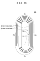
- an electrode assembly 20 (a wound electrode assembly 80) of a cell described in Patent Literature 1 (Japanese Patent Application Laid-Open No. 2010-287513 ) is such that an inner-circumferential end portion 22d (indicated by a solid line) of the negative electrode 22 covers an inner-circumferential end portion 21d (indicated by a solid line) of the positive electrode 21 and is wound so that the negative electrode 22 is disposed on an innermost circumference of the electrode assembly 20.
- an electrode assembly 20 (an electrode assembly group 2) of a cell described in Patent Literature 2 (Japanese Patent Application Laid-Open No.
- an inner-circumferential end portion 21d (indicated by a solid line) of the positive electrode 21 covers an inner-circumferential end portion 22d (indicated by a solid line) of the negative electrode 22 and is wound so that the positive electrode 21 is disposed on an innermost circumference of the electrode assembly 20.
- the number of windings of the positive electrode 21 and the negative electrode 22 is smaller than it really is in order to make the configuration of winding clearly understandable. In an actual electrode assembly 20, winding is performed in a larger number and in a denser manner.
- the illustration of the separator 23 is omitted.
- Each of the electrode assemblies 20, 20 is of a flat shape.
- the electrode assembly 20 has first and second flat portions 20a, 20a, and first and second curved portions 20b, 20b.
- the first and second flat portions 20a, 20a are opposed to each other.
- the first and second curved portions 20b, 20b connect end portions of the first and second flat portions 20a, 20a together.
- the electrode assembly 20 described in Patent Literature 1 is wound in such a manner that a leading-end edge of the inner-circumferential end portion 22d of the negative electrode 22 is positioned in the flat portion 20a.
- the electrode assembly 20 described in Patent Literature 2 is wound in such a manner that a leading-end edge of the inner-circumferential end portion 21d of the positive electrode 21 is positioned in the flat portion 20a. That is, in each electrode assembly 20, the leading-end edge of the inner-circumferential end portion of the electrode disposed on the innermost circumference is positioned in the flat portion 20a.
- the inner-circumferential end portion 22d of the negative electrode 22 is apt to move in the space at the winding center (indicated by a dashed-two dotted line). In association with this, also the inner-circumferential end portion 21d of the positive electrode 21 is apt to move (indicated by a dashed-two dotted line). In the electrode assembly 20 described in Patent Literature 2, the inner-circumferential end portion 21d of the positive electrode 21 is apt to move in the space at the winding center (indicated by a dashed-two dotted line). In association with this, also the inner-circumferential end portion 22d of the negative electrode 22 is apt to move (indicated by a dashed-two dotted line).
- the interelectrode distance between the positive electrode 21 and the negative electrode 22 increases.
- the inner-circumferential end portion 22d of the negative electrode 22 may be bent, and the inner-circumferential end portion 21d of the positive electrode 21 may be bent.
- the function of the electrode in this area may be impaired. For this reason, a problem arises that the capacity of the cell decreases.
- An object of the present invention is to provide an electric storage device capable of preventing an inner-circumferential end portion of a negative electrode and an inner-circumferential end portion of a positive electrode from moving in the space at the winding center of an electrode assembly.
- An electric storage device includes an electrode assembly, in which a positive electrode and a negative electrode in the shape of a sheet are wound with a separator sandwiched therebetween, wherein the electrode assembly has a flat shape and includes a first flat portion and a second flat portion, which are opposed to each other, and a first curved portion and a second curved portion which connect end portions of the first and second flat portions together, one of the positive electrode and the negative electrode covers an inner-circumferential end portion of the other electrode and is disposed on an innermost circumference of the electrode assembly, and an inner-circumferential end portion of the one of the electrodes causes an elastic force to act outwardly on the other electrode.
- An electric storage device includes an electrode assembly, in which a positive electrode and a negative electrode in the shape of a sheet are wound with a separator sandwiched therebetween.
- the electrode assembly includes a first flat portion and a second flat portion, which are opposed to each other, and a first curved portion and a second curved portion which connect end portions of the first and second flat portions together.
- the electrode assembly has a flat shape.
- One of the positive electrode and the negative electrode covers an inner-circumferential end portion of the other electrode and is disposed on an innermost circumference of the electrode assembly.
- An inner-circumferential end portion of the one of the electrodes causes an elastic force to act outwardly on the other electrode.
- a leading-end edge of the inner-circumferential end portion of the one of the electrodes may be positioned in an area of one of the first and second curved portions beyond a fold-back point of the one of the first and second curved portions.
- the leading end portion of the inner-circumferential end portion of one of the electrodes is curved along an inner surface of the one of the first and second curved portions. For this reason, the leading end portion of the inner-circumferential end portion of one of the electrodes generates an elastic force with which this leading end portion tends to go back straight and spread outwardly, whereby this leading end portion is kept in a state in which the leading end portion extends along the inner surface of the electrode assembly. Therefore, the inner-circumferential end portion of one of the electrodes does not move in the space at the winding center.
- each of the first and second curved portions may have the shape of a circular arc with a radius of curvature of not less than 0.1 mm.
- a leading-end edge of the inner-circumferential end portion of the other electrode may be positioned in the one of the first and second flat portions.
- the one of the electrodes may have a protruding portion, a restraining portion, and a current collector connected to the restraining portion.
- the protruding portion protrudes from a side end of the other electrode in a direction along the winding center of the electrode assembly.
- the restraining portion is formed by bundling areas of the protruding portion spaced from the inner-circumferential end portion of the one of the electrodes.
- the restraining portion may include a first restraining portion on one side of the protruding portion and a second restraining portion on the other side of the protruding portion with the winding center of the electrode assembly therebetween.
- the first restraining portion restrains the one side of the protruding portion.
- the second restraining portion restrains the other side of the protruding portion.
- the restraining portion may be formed at a position of the first and second flat portions, the position being shifted to (located close to) the other curved portion on the side opposite to the one of the first and second curved portions in which the leading-end edge of the inner-circumferential end portion of the one of the electrodes is positioned.
- the one of the electrodes may be a negative electrode and the other electrode may be a positive electrode.
- a cell which is an embodiment of the electric storage device of the present invention will be described in detail below with reference to FIGS. 1 to 7 .
- the cell is provided with a case 10 made of metal, an electrode assembly 20, a positive electrode terminal 31 and a negative electrode terminal 32, a current collector 40, a backing member 50, and the like.
- the electrode assembly 20 is accommodated in the interior of the case 10.
- the positive electrode terminal 31 and the negative electrode terminal 32 protrude from the interior of the case 10 to outside.
- the current collector 40 connects each end portion of the electrode assembly 20 to each of the electrode terminals 31, 32.
- the backing member 50 is connected to an end portion of the electrode assembly 20 in conjunction with the current collector 40.
- the case 10 is formed by a combination of a case body 11 in the shape of a bottomed square cylinder having an opening and a cover plate 12 with which the opening of the case body 11 is sealed. After the installation of both members 11, 12, an end edge of the opening of the case body 11 and an outer circumferential edge of the cover plate 12 are welded. Whereby, both members 11, 12 are integrated with each other.
- the case body 11 has a pair of opposed side plate portions 11b and a pair of opposed end plate portions 11c standing upright on peripheral edges of a rectangular bottom portion 11a.
- the pair of end plate portions 11c of the case body 11 are formed so as to be smaller in width (than the pair of side plate portions 11b). In this way, the case body 11 is formed into the shape of a thin rectangular cylinder having a small depth and closed at its bottom.
- Electrodes 31 and 32 Holes (not numbered) through which the electrode terminals 31 and 32 are passed are formed in the cover plate 12.
- the electrode terminals 31 and 32 are passed through the holes of the cover plate 12 and fixed on the cover plate 12 like rivets. As a result, outer end portions of the electrode terminals 31 and 32 project from the cover plate 12, and inner end portions of the electrode terminals 31 and 32 project into the interior of the case 10.
- the electrode assembly 20 has a flat shaped wound structure including the positive electrode 21, the negative electrode 22, and the separator 23. In this sense, the electrode assembly 20 is the same as conventional electrode assemblies. Therefore, the description of the electrode assembly 20 and the description of the positive electrode 21, the negative electrode 22, and the separator 23 in the Background section of this specification is incorporated herein by reference as a description of the electrode assembly 20 of this embodiment.
- the electrode assembly 20 of this embodiment differs from the electrode assembly described in Patent Literature 1 and the electrode assembly described in Patent Literature 2 in that the electrode assembly 20 of this embodiment is wound in such a manner that the inner-circumferential end portion 22d of the negative electrode 22 covers the inner-circumferential end portion 21d of the positive electrode 21 and the negative electrode 22 is disposed in the innermost circumference of the electrode assembly 20.
- the electrode assembly 20 differs from the electrode assembly in Patent Literature 1 or 2 in that the electrode assembly 20 of this embodiment is wound in such a manner that a leading-end edge 22d' of the inner-circumferential end portion 22d of the negative electrode 22 is positioned in an area of the curved portion 20b beyond the fold-back point C.
- the number of windings of the positive electrode 21 and the negative electrode 22 is smaller than it really is in order to make the configuration of winding clearly understandable. However, in an actual electrode assembly 20, winding is performed in a larger number and in a denser manner. In FIG. 3 , the illustration of the separator 23 is omitted.
- the curved portion 20b is semicircular. That is, the curved portion 20b has an angle range of 180 degrees. Therefore, the fold-back point C is located at a point of 90 degrees, which is a half of this value.
- the flat portion 20a which is arranged on the right side of the figure
- the flat portion 20a which is arranged on the left side of the figure
- the curved portion 20b which is arranged on the upper side of the figure (the opening side of the case body 11)
- the curved portion 20b, which is arranged on the lower side of the figure (the bottom portion 11a of the case body 11) is referred to as a second curved portion 20b2
- the leading-end edge 22d' of the inner-circumferential end portion 22d of the negative electrode 22 is positioned in an angle range from the fold-back point C of the second
- a leading-end edge 21d' of the inner-circumferential end portion 21d of the positive electrode 21 is positioned in the first flat portion 20a1. More specifically, the leading-end edge 21d' of the inner-circumferential end portion 21d of the positive electrode 21 is positioned in an area which is closer to the terminal point of the first flat portion 20a1 (a connecting point between the first flat portion 20a1 and the second curved portion 20b2) in the first flat portion 20a1 than the middle point in the first flat portion 20a1.
- the leading end portion of the inner-circumferential end portion 22d of the negative electrode 22 is curved in the shape of a circular arc along the inner surface of the curved portion 20b.
- the leading end portion of the inner circumferential end portion 21d of the positive electrode 21 is not curved, but is straight along the inner surface of the flat portion 20a.
- the first and second curved portions 20b1, 20b2 have both the shape of a circular arc with a radius of curvature of not less than 0.1 mm.
- the positive electrode 21 and the negative electrode 22 are shifted laterally in the width direction.
- the positive-electrode active material layer-non-formed portion 21c protrudes from the side end of the negative electrode 22
- the negative-electrode active material layer-non-formed portion 22c protrudes from the side end of the positive electrode 21.
- the electrode assembly 20 has a protruding portion 20c of the positive electrode on one-end side and a protruding portion 20c of the negative electrode on the other-end side.
- the protruding portion 20c of the positive electrode has a restraining portion 20d and an inclined portion 20e.
- the protruding portion 20c of the negative electrode also has a restraining portion 20d and an inclined portion 20e.
- Each restraining portion 20d is formed by bundling leading end portions of this protruding portion 20c by mutual tight contact in the stage prior to joining to the current collector 40.
- Each inclined portion 20e inclines from the base end side of the protruding portion 20c toward the restraining portion 20d.
- a current collector 40 for the positive electrode is disposed on one surface of the restraining portion 20d in the protruding portion 20c of the positive electrode, and a backing plate 50 is disposed on the other surface of the restraining portion 20d.
- the current collector 40 for the positive electrode and the backing plate 50 each are made of, for example, aluminum or an aluminum alloy.
- the current collector 40 for the positive electrode and the backing plate 50, along with the restraining portion 20d, are joined by ultrasonic joining, for example.
- a current collector 40 for the negative electrode is disposed on one surface of the restraining portion 20d in the protruding portion 20c of the negative electrode, and a backing plate 50 is disposed on the other surface of the restraining portion 20d.
- the current collector 40 and the backing plate 50 of the negative electrode each are made of, for example, copper or a copper alloy.
- the current collector 40 and the backing plate 50 for the negative electrode, along with the restraining portion 20d, are joined by ultrasonic joining, for example.
- the electrode assembly 20 fabricated in the manner as described above is accommodated in the case 10 such that the winding axis is in parallel to the bottom portion 11a of the case 10. That is, each of the pair of protruding portions 20c, 20c of the electrode assembly 20 faces each end plate portion 11c of the case 10.
- the current collector 40 includes the current collector 40 for the positive electrode and the current collector 40 for the negative electrode.
- the current collector 40 for the positive electrode connects the protruding portion 20c of the positive electrode of the electrode assembly 20 and the positive electrode terminal 31.
- the current collector 40 for the negative electrode connects the protruding portion 20c of the negative electrode of the electrode assembly 20 and the negative electrode terminal 32.
- the current collector 40 is provided with an inner connecting portion 41, an electrode attachment portion 42, and an intermediate portion 43. To the inner connecting portion 41, the positive electrode terminal 31 or the negative electrode terminal 32 is connected by being caulked like a rivet or by welding.
- the electrode attachment portion 42 is directly or indirectly connected to the restraining portion 20d in the protruding portion 20c of the positive electrode of the electrode assembly 20 or to the restraining portion 20d in the protruding portion 20c of the negative electrode.
- the intermediate portion 43 connects the inner connecting portion 41 and the electrode attachment portion 42 to each other.
- the current collector 40 is formed from one sheet of metal material.
- the current collector 40 has a deformed letter L shape as seen from the front.
- the current collector 40 for the positive electrode is made of, for example, aluminum or an aluminum alloy
- the current collector 40 for the negative electrode is made of, for example, copper or a copper alloy.
- the inner connecting portion 41 and the electrode attachment portion 42 extend perpendicularly with the intermediate portion 43 as a fold line (in the letter L as seen from the front).
- the inner connecting portion 41 is disposed along the inner surface of the cover plate 12 of the case 10 in a condition in which the inner connecting portion 41 is insulated from the inner surface of the cover plate 12 of the case 10.
- a through hole 41a into which the inner end portion of the positive electrode terminal 31 or of the negative electrode terminal 32is inserted is provided in the leading end portion of the inner connecting portion 41.
- the electrode attachment portion 42 is disposed between the end portion of the electrode assembly 20 and the end plate portion 11c of the case body 11. As shown in FIGS. 4A to 4C , the electrode attachment portion 42 is provided with an opening 42a. At both edges of the opening 42a, two connection pieces 42b, 42b are provided in a protruding manner in the same direction as the inner connecting portion 41.
- the opening 42a and the connection pieces 42b, 42b are formed, for example, by making a longitudinal incision in a band plate before the forming of the electrode attachment portion 42 and raising both sides of this incision.
- the protruding portion 20c of the electrode assembly 20 is formed in a pair for both the positive electrode and the negative electrode. That is, the protruding portion 20c of the electrode assembly 20 includes a first protruding portion 20c and a second protruding portion 20c, which are disposed with the winding center of the electrode assembly 20 located therebetween.
- the first protruding portion 20c and the second protruding portion 20c of the current collector 40 are opposed to each other, with a gap therebetween. Therefore, the pair of connection pieces 42b, 42b of the current collector 40 is inserted into the space between the first protruding portion 20c and the second protruding portion 20c.
- connection pieces 42b is attached along the inner surface of the restraining portion 20d of the first protruding portion 20c, and the other connection piece 42b is attached along the inner surface of the restraining portion 20d of the second protruding portion 20c. Furthermore, a first backing member 50 is attached along the outer surface of the restraining portion 20d of the first protruding portion 20c, and a second backing member 50 is attached along the outer surface of the restraining portion 20d of the second protruding portion 20c.
- an anvil is set on the connection piece 42b and an ultrasonic oscillator is set to the backing member 50. And the ultrasonic oscillator is caused to perform ultrasonic oscillation, whereby frictional heat is generated and the connection piece 42b and the backing member 50, along with the restraining portion 20d, are ultrasonic welded.
- connection pieces 42b, 42b of the current collector 40 and first and second backing members 50, 50 are disposed in positions shifted to (located close to) the first curved portions 20b1 (the curved portion 20b on the opening side of the case body 11) in the first and second flat portions 20a1, 20a2. Because the leading-end edge 22d' of the inner-circumferential end portion 22d of the negative electrode 22 on an innermost circumference of the electrode assembly 20 is positioned in the second curved portion 20b2 (the curved portion 20b on the bottom portion 11a side of the case body 11).
- each set of the pair of connection pieces 42b, 42b of the current collector 40 and first and second backing members 50, 50 is joined to the restraining portions 20d, 20d of the electrode assembly 20 in areas spaced from the inner-circumferential end portion 22d of the negative electrode 22.
- the negative electrode 22 is disposed on an innermost circumference of the electrode assembly 20, covering the inner-circumferential end portion 21d of the positive electrode 21, and the leading-end edge 22d' of the inner-circumferential end portion 22d of the negative electrode 22 is positioned in an area of the second curved portion 20b2 beyond the fold-back point C.
- the leading end portion of the inner-circumferential end portion 22d of the negative electrode 22 is curved in the shape of a circular arc along the inner surface of the second curved portion 20b2.
- the leading end portion of the inner-circumferential end portion 22d of the negative electrode 22 generates an elastic force F with which this leading end portion tends to go back straight and spread outwardly, whereby this leading end portion is kept in a condition in which the leading end portion extends along the inner surface of the electrode assembly 20. Therefore, the inner-circumferential end portion 22d of the negative electrode 22 does not move in the space at the winding center. For this reason, such phenomena as described below may not occur: an increase in the interelectrode distance between the positive electrode 21 and the negative electrode 22 and bending of the inner-circumferential end portion 22d of the negative electrode 22, with the result that the function of the electrode in this area is impaired and the capacity of the cell decreases.
- each set of the pair of connection pieces 42b, 42b of the current collector 40 and first and second backing members 50, 50 is joined to the restraining portions 20d, 20d of the electrode assembly 20 in areas spaced from the inner-circumferential end portion 22d of the negative electrode 22.
- the sets of the connection pieces 42b and the backing members 50 are disposed in places where the sets of the connection pieces 42b and the backing members 50 sandwich the inner-circumferential end portion 22d of the negative electrode 22, the inner-circumferential end portion 22d of the negative electrode 22 is restrained and therefore the free movement of the inner-circumferential end portion 22d of the negative electrode 22 does not occur.
- each set of the pair of connection pieces 42b, 42b of the current collector 40 and first and second backing members 50, 50 is spaced from the inner-circumferential end portion 22d of the negative electrode 22, it is very meaningful to dispose the inner-circumferential end portion 22d of the negative electrode 22 in the above-described position in order to prevent the free movement of the inner-circumferential end portion 22d of the negative electrode 22.
- the first and second curved portions 20b1, 20b2 of the electrode assembly 20 have both the shape of a circular arc with a radius of curvature of not less than 0.1 mm.
- the radius of curvature is less than 0.1 mm, the space at the winding center of the electrode assembly 20 is very narrow and the free movement of the inner-circumferential end portion 22d of the negative electrode 22 is not apt to occur.
- the radius of curvature is not less than 0.1 mm and the space at the winding center of the electrode assembly 20 is wide, it is very meaningful to dispose the inner-circumferential end portion 22d of the negative electrode 22 in the above-described position in order to prevent the free movement of the inner-circumferential end portion 22d of the negative electrode 22.
- the leading-end edge 21d' of the inner-circumferential end portion 21d of the positive electrode 21 is positioned in the first flat portion 20a1.
- lithium transition metal composite compounds and the like used as positive-electrode active materials are harder than carbon materials and the like used as negative-electrode active materials.
- the positive-electrode active material layer 21b is harder than the negative-electrode active material layer 22b. Therefore, in the case where the inner-circumferential end portion 21d of the positive electrode 21 is wound with a small radius of curvature, the positive-electrode active material layer 21b may sometimes be broken or exfoliate from the positive-electrode current collector substrate 21a.
- the leading-end edge 21d' of the inner-circumferential end portion 21d of the positive electrode 21 is disposed in the flat portion 20a, whereby such problems do not arise.
- the first and second protruding portions 20c, 20c disposed with the winding center of the electrode assembly 20 located therebetween two (a pair of) restraining portions 20d, 20d are provided.
- the first restraining portion 20d is formed in the first protruding portion 20c.
- the second restraining portion 20d is formed in the second protruding portion 20c.
- two restraining portions 20d it is possible to make the inclination of the inclined portion 20e gentle compared to the case where one restraining portion 20d is provided. For this reason, it is possible to make the width of the uncoated portion narrow and hence it is possible to increase the cell capacity.
- the electric storage device of the present invention is not limited to the configuration of the above-described embodiment.
- the electric storage device of the present invention is not limited to the operational advantages described above, either.
- Various changes may be made in the electric storage device of the present invention without departing from the spirit and scope of the present invention.
- the negative electrode 22 that is disposed on an innermost circumference of the electrode assembly 20, and the movement (stagger) of the inner-circumferential end portion 22d of the negative electrode 22 is exclusively the object of prevention.
- the positive electrode 21 covers the inner-circumferential end portion 22d of the negative electrode 22, is disposed on an innermost circumference of the electrode assembly 20 and the leading-end edge 21d' of the inner-circumferential end portion 21d of the positive electrode 21 may be disposed in an area beyond the fold-back point C in the curved portion 20b.
- the leading-end portion of the inner-circumferential end portion 21d of the positive electrode 21 is curved in the shape of a circular arc along the inner surface of the curved portion 20b.
- a positive-electrode active material layer (a positive-electrode active material coated portion) 21b is formed on both surfaces of the positive-electrode current collector substrate 21a, a positive-electrode active material layer (a positive-electrode active material coated portion) 21b formed on the surface of the positive-electrode current collector substrate 21a on the winding center side is exposed in the space at the winding center.
- the precipitation of dendrite becomes a problem.
- a positive-electrode active material layer (a positive-electrode active material coated portion) 21b be formed only on one surface of the positive-electrode current collector substrate 21a and that a positive-electrode active material layer (a positive-electrode active material coated portion) 21b be not present on the surface of the positive-electrode current collector substrate 21a on the winding center side.
- an active material having a high potential, such as lithium titanate in the negative electrode, the precipitation of dendrite becomes less apt to occur considerably.
- a positive-electrode active material layer (a positive-electrode active material coated portion) 21b may be formed on both surfaces of the positive-electrode current collector substrate 21a also in the part of the positive electrode 21 disposed on an innermost circumference of the electrode assembly 20.
- the leading-end edge of the inner-circumferential end portion of the electrode on an innermost circumference is positioned in the curved portion 20b of the electrode assembly 20 on the bottom portion 11a side of the case body 11.
- the current collector 40 also the backing member 50 is one aspect of the current collector
- the leading-end edge of the inner-circumferential end portion of the electrode on an innermost circumference may be positioned in the curved portion 20b of the electrode assembly 20 on the opening side of the case body 11, whereby the current collector 40 is connected in the flat portion 20a near the curved portion 20b of the electrode assembly 20 on the bottom portion 11a side of the case body 11, which is the side opposite to the opening side of the case body 11.
- the current collector 40 may be connected in any area of the flat portion 20a of the first and second flat portions 20a1, 20a2, as long as this flat portion 20a has the inner-circumferential end portion of the electrode on an innermost circumference not positioned therein.
- the connection piece 42b of the current collector 40 may also be connected in the area of the flat portion 20a near the curved portion 20b where the leading-end edge of the inner-circumferential end portion of the electrode on an innermost circumference is positioned.
- connection piece 42b of the current collector 40 is disposed on the inner surface of the restraining portion 20d of the protruding portion 20c of the electrode assembly 20 and the backing member 50 is disposed on the outer surface of this restraining portion 20d.
- the connection piece 42b of the current collector 40 is disposed on the outer surface of the restraining portion 20d of the protruding portion 20c of the electrode assembly 20 and the backing member 50 is disposed on the inner surface of the restraining portion 20d.
- a set of the connection piece 42b of the current collector 40 and backing member 50 is connected to the electrode assembly 20.
- the connecting form of the current collector 40 and the electrode assembly 20 is not limited to this.
- connection piece 42b of the current collector 40 and backing member 50 are ultrasonic joined.
- the joining method is not limited to this.
- joining can be performed by various measures such as resistance welding, laser welding and caulking.
- it is preferable to perform joining by ultrasonic joining.
- the embodiment has been described in the context of a lithium-ion secondary battery cell.
- the type and size (capacity) of a battery cell may be arbitrarily selected.
- the present invention is not limited to the lithium-ion secondary battery cell.
- the present invention can also be applied to various kinds of secondary cells, primary cells, and capacitors such as an electric double layer capacitor.
Landscapes
- Engineering & Computer Science (AREA)
- Power Engineering (AREA)
- Microelectronics & Electronic Packaging (AREA)
- Manufacturing & Machinery (AREA)
- Chemical & Material Sciences (AREA)
- Electrochemistry (AREA)
- Chemical Kinetics & Catalysis (AREA)
- General Chemical & Material Sciences (AREA)
- Materials Engineering (AREA)
- Secondary Cells (AREA)
- Electric Double-Layer Capacitors Or The Like (AREA)
- Connection Of Batteries Or Terminals (AREA)
- Primary Cells (AREA)
Description
- The present invention relates to an electric storage device.
- Rechargeable electric storage devices have recently been adopted as the power sources of vehicles (e.g., an automobile and a motorcycle) and various devices (e.g., a portable terminal and a laptop personal computer). Examples of the electric storage devices include battery cells (e.g., a lithium-ion battery cell and a nickel-metal-hydride battery cell), and capacitors (e.g., an electric double layer capacitor). Various types of cells are provided. As one of such cells, there is available a cell which is provided with an electrode assembly in which a positive electrode and a negative electrode in the shape of a sheet are wound with a separator sandwiched therebetween and a current collector connected to this electrode assembly.
- As shown in
FIG. 9C , apositive electrode 21, anegative electrode 22 and aseparator 23 are stacked in the order of theseparator 23, thenegative electrode 22, theseparator 23 and thepositive electrode 21. These are wound in cylindrical shape to have thepositive electrode 21 located outside. After that, the side surfaces of the cylindrical shape are pressed from both sides, whereby the side surfaces are crushed into a flat shape and deformed. Thus, the electrode assembly is fabricated. Alternatively, the electrode assembly is fabricated such that a laminate of theseparator 23, thenegative electrode 22, theseparator 23, and thepositive electrode 21, which are stacked in this order from the inner side, is wound into a flat shape. - As shown in
FIG. 9A , thepositive electrode 21 is provided with a positive-electrode active material layer (a positive-electrode active material coated portion) 21b on each of both surfaces of a positive-electrodecurrent collector substrate 21a. This positive-electrode active material layer is formed, for example, by applying a positive-electrode active material paste to one surface of the positive-electrodecurrent collector substrate 21a, drying the paste, then similarly applying a positive-electrode active material paste to the other surface of the positive-electrodecurrent collector substrate 21a and drying the paste. The positive-electrodecurrent collector substrate 21a is formed from, for example, long strip-shaped aluminum foil. - As shown in
FIG. 9B , thenegative electrode 22 is provided with a negative-electrode active material layer (a negative-electrode active material coated portion) 22b on each of both surfaces of a negative-electrodecurrent collector substrate 22a. This negative-electrode active material layer is formed, for example, by applying a negative-electrode active material paste to one surface of the negative-electrodecurrent collector substrate 22a, drying the paste, then similarly applying a negative-electrode active material paste to the other surface of the negative-electrodecurrent collector substrate 22a and drying the paste. The negative-electrodecurrent collector substrate 22a is formed from, for example, long strip-shaped copper foil. - More specifically, with the exception of one end portion of the positive-electrode
current collector substrate 21a in the width direction, thepositive electrode 21 is, for example, coated with a positive-electrode active material paste on both surfaces. Whereby, thepositive electrode 21 is provided with the positive-electrodeactive material layer 21b on each of both surfaces of the positive-electrodecurrent collector substrate 21a except this end portion. For this reason, in this end portion, the positive-electrodecurrent collector substrate 21a (a positive-electrode active material layer-non-formedportion 21c) is exposed. On the other hand, with the exception of one end portion of the negative-electrodecurrent collector substrate 22a in the width direction, thenegative electrode 22 is, for example, coated with a negative-electrode active material paste on both surfaces. Whereby, thenegative electrode 22 is provided with the negative-electrodeactive material layer 22b on each of both surfaces of the negative-electrodecurrent collector substrate 22a except this end portion. For this reason, in this end portion, the negative-electrodecurrent collector substrate 22a (a negative-electrode active material layer-non-formedportion 22c) is exposed. - As shown in
FIG. 9C , theseparator 23 physically isolates thepositive electrode 21 and thenegative electrode 22 from each other and holds an electrolyte. - In order to prevent the precipitation of dendrite and the like, the negative-electrode
active material layer 22b is applied with a larger width than the positive-electrodeactive material layer 21b. Theseparator 23, which provides insulation between thepositive electrode 21 and thenegative electrode 22, has a larger width than the positive-electrodeactive material layer 21b and the negative-electrodeactive material layer 22b. However, theseparator 23 has a width not covering the positive-electrode active material layer-non-formedportion 21c or the negative-electrode active material layer-non-formedportion 22c, which protrude widthwise. - As shown in the conceptual diagram of
FIG. 10 , an electrode assembly 20 (a wound electrode assembly 80) of a cell described in Patent Literature 1 (Japanese Patent Application Laid-Open No.2010-287513 circumferential end portion 22d (indicated by a solid line) of thenegative electrode 22 covers an inner-circumferential end portion 21d (indicated by a solid line) of thepositive electrode 21 and is wound so that thenegative electrode 22 is disposed on an innermost circumference of theelectrode assembly 20. As shown in the conceptual diagram ofFIG. 11 , an electrode assembly 20 (an electrode assembly group 2) of a cell described in Patent Literature 2 (Japanese Patent Application Laid-Open No.2008-251256 circumferential end portion 21d (indicated by a solid line) of thepositive electrode 21 covers an inner-circumferential end portion 22d (indicated by a solid line) of thenegative electrode 22 and is wound so that thepositive electrode 21 is disposed on an innermost circumference of theelectrode assembly 20. InFIGS. 10 and11 , the number of windings of thepositive electrode 21 and thenegative electrode 22 is smaller than it really is in order to make the configuration of winding clearly understandable. In anactual electrode assembly 20, winding is performed in a larger number and in a denser manner. InFIGS. 10 and11 , the illustration of theseparator 23 is omitted. - Each of the electrode assemblies 20, 20 is of a flat shape. The
electrode assembly 20 has first and secondflat portions curved portions flat portions curved portions flat portions electrode assembly 20 described in Patent Literature 1 is wound in such a manner that a leading-end edge of the inner-circumferential end portion 22d of thenegative electrode 22 is positioned in theflat portion 20a. Theelectrode assembly 20 described inPatent Literature 2 is wound in such a manner that a leading-end edge of the inner-circumferential end portion 21d of thepositive electrode 21 is positioned in theflat portion 20a. That is, in eachelectrode assembly 20, the leading-end edge of the inner-circumferential end portion of the electrode disposed on the innermost circumference is positioned in theflat portion 20a. - In the
electrode assembly 20 described in Patent Literature 1, the inner-circumferential end portion 22d of thenegative electrode 22 is apt to move in the space at the winding center (indicated by a dashed-two dotted line). In association with this, also the inner-circumferential end portion 21d of thepositive electrode 21 is apt to move (indicated by a dashed-two dotted line). In theelectrode assembly 20 described inPatent Literature 2, the inner-circumferential end portion 21d of thepositive electrode 21 is apt to move in the space at the winding center (indicated by a dashed-two dotted line). In association with this, also the inner-circumferential end portion 22d of thenegative electrode 22 is apt to move (indicated by a dashed-two dotted line). - In the event where the inner-
circumferential end portion 22d of thenegative electrode 22 moves and the inner-circumferential end portion 21d of thepositive electrode 21 moves, the interelectrode distance between thepositive electrode 21 and thenegative electrode 22 increases. In addition, the inner-circumferential end portion 22d of thenegative electrode 22 may be bent, and the inner-circumferential end portion 21d of thepositive electrode 21 may be bent. Thus, the function of the electrode in this area may be impaired. For this reason, a problem arises that the capacity of the cell decreases. - An object of the present invention is to provide an electric storage device capable of preventing an inner-circumferential end portion of a negative electrode and an inner-circumferential end portion of a positive electrode from moving in the space at the winding center of an electrode assembly.
- An electric storage device according to an aspect of the present invention includes an electrode assembly, in which a positive electrode and a negative electrode in the shape of a sheet are wound with a separator sandwiched therebetween, wherein the electrode assembly has a flat shape and includes a first flat portion and a second flat portion, which are opposed to each other, and a first curved portion and a second curved portion which connect end portions of the first and second flat portions together, one of the positive electrode and the negative electrode covers an inner-circumferential end portion of the other electrode and is disposed on an innermost circumference of the electrode assembly, and an inner-circumferential end portion of the one of the electrodes causes an elastic force to act outwardly on the other electrode.
-
-
FIG. 1 is a partially broken front view of a cell, which is an embodiment of an electric storage device of the present invention; -
FIG. 2 is a perspective view of a structure in a case of the cell; -
FIG. 3 is a longitudinal sectional conceptual diagram of an electrode assembly of the cell; -
FIG. 4A is a front view of a current collector of the cell; -
FIG. 4B is a side view of the current collector of the cell; -
FIG. 4C is a perspective view of the current collector of the cell; -
FIG. 5A is a transverse cross-sectional conceptual diagram of electrode assemblies; -
FIG. 5B is a transverse cross-sectional conceptual diagram of the electrode assembly in a state in which end portions thereof are bundled; -
FIG. 5C is a transverse cross-sectional conceptual diagram of the electrode assembly in a state in which current collectors are joined to end portions of the electrode assembly; -
FIG. 6 is a cross sectional view taken along the line A-A ofFIG. 1 ; -
FIG. 7 is a cross sectional view taken along the line B-B ofFIG. 1 ; -
FIG. 8 is a longitudinal sectional conceptual diagram of an electrode assembly of another embodiment; -
FIG. 9A is an explanatory diagram to explain each element of a positive electrode plate forming a general electrode assembly; -
FIG. 9B is an explanatory diagram to explain each element of a negative electrode plate forming the electrode assembly; -
FIG. 9C is an explanatory diagram to explain a positional relationship in a width-direction of a positive electrode plate, a negative electrode plate, and separators; -
FIG. 10 is a longitudinal sectional conceptual diagram of a conventional electrode assembly; and -
FIG. 11 is a longitudinal sectional conceptual diagram of another conventional electrode assembly. - An electric storage device includes an electrode assembly, in which a positive electrode and a negative electrode in the shape of a sheet are wound with a separator sandwiched therebetween. The electrode assembly includes a first flat portion and a second flat portion, which are opposed to each other, and a first curved portion and a second curved portion which connect end portions of the first and second flat portions together. The electrode assembly has a flat shape. One of the positive electrode and the negative electrode covers an inner-circumferential end portion of the other electrode and is disposed on an innermost circumference of the electrode assembly. An inner-circumferential end portion of the one of the electrodes causes an elastic force to act outwardly on the other electrode.
- As an aspect of the electric storage device of the present invention, a leading-end edge of the inner-circumferential end portion of the one of the electrodes may be positioned in an area of one of the first and second curved portions beyond a fold-back point of the one of the first and second curved portions.
- According to this configuration, the leading end portion of the inner-circumferential end portion of one of the electrodes is curved along an inner surface of the one of the first and second curved portions. For this reason, the leading end portion of the inner-circumferential end portion of one of the electrodes generates an elastic force with which this leading end portion tends to go back straight and spread outwardly, whereby this leading end portion is kept in a state in which the leading end portion extends along the inner surface of the electrode assembly. Therefore, the inner-circumferential end portion of one of the electrodes does not move in the space at the winding center.
- As another aspect of the electric storage device of the present invention, each of the first and second curved portions may have the shape of a circular arc with a radius of curvature of not less than 0.1 mm.
- As a further aspect of the electric storage device of the present invention, a leading-end edge of the inner-circumferential end portion of the other electrode may be positioned in the one of the first and second flat portions.
- As an even further aspect of the electric storage device of the present invention, the one of the electrodes may have a protruding portion, a restraining portion, and a current collector connected to the restraining portion. The protruding portion protrudes from a side end of the other electrode in a direction along the winding center of the electrode assembly. The restraining portion is formed by bundling areas of the protruding portion spaced from the inner-circumferential end portion of the one of the electrodes.
- In this case, the restraining portion may include a first restraining portion on one side of the protruding portion and a second restraining portion on the other side of the protruding portion with the winding center of the electrode assembly therebetween. The first restraining portion restrains the one side of the protruding portion. The second restraining portion restrains the other side of the protruding portion.
- The restraining portion may be formed at a position of the first and second flat portions, the position being shifted to (located close to) the other curved portion on the side opposite to the one of the first and second curved portions in which the leading-end edge of the inner-circumferential end portion of the one of the electrodes is positioned.
- Furthermore, as a further aspect of the electric storage device of the present invention, the one of the electrodes may be a negative electrode and the other electrode may be a positive electrode.
- As described above, according to the present invention, it is possible to prevent an inner-circumferential end portion of a negative electrode and an inner-circumferential end portion of a positive electrode from moving in the space at the winding center of an electrode assembly.
- A cell which is an embodiment of the electric storage device of the present invention will be described in detail below with reference to
FIGS. 1 to 7 . - As shown in
FIGS. 1 and2 , the cell is provided with acase 10 made of metal, anelectrode assembly 20, apositive electrode terminal 31 and anegative electrode terminal 32, acurrent collector 40, a backingmember 50, and the like. Theelectrode assembly 20 is accommodated in the interior of thecase 10. Thepositive electrode terminal 31 and thenegative electrode terminal 32 protrude from the interior of thecase 10 to outside. Thecurrent collector 40 connects each end portion of theelectrode assembly 20 to each of theelectrode terminals member 50 is connected to an end portion of theelectrode assembly 20 in conjunction with thecurrent collector 40. - The
case 10 is formed by a combination of acase body 11 in the shape of a bottomed square cylinder having an opening and acover plate 12 with which the opening of thecase body 11 is sealed. After the installation of bothmembers case body 11 and an outer circumferential edge of thecover plate 12 are welded. Whereby, bothmembers - The
case body 11 has a pair of opposedside plate portions 11b and a pair of opposedend plate portions 11c standing upright on peripheral edges of arectangular bottom portion 11a. The pair ofend plate portions 11c of thecase body 11 are formed so as to be smaller in width (than the pair ofside plate portions 11b). In this way, thecase body 11 is formed into the shape of a thin rectangular cylinder having a small depth and closed at its bottom. - Holes (not numbered) through which the
electrode terminals cover plate 12. Theelectrode terminals cover plate 12 and fixed on thecover plate 12 like rivets. As a result, outer end portions of theelectrode terminals cover plate 12, and inner end portions of theelectrode terminals case 10. - The
electrode assembly 20 has a flat shaped wound structure including thepositive electrode 21, thenegative electrode 22, and theseparator 23. In this sense, theelectrode assembly 20 is the same as conventional electrode assemblies. Therefore, the description of theelectrode assembly 20 and the description of thepositive electrode 21, thenegative electrode 22, and theseparator 23 in the Background section of this specification is incorporated herein by reference as a description of theelectrode assembly 20 of this embodiment. - As is apparent from
FIG. 3 , theelectrode assembly 20 of this embodiment differs from the electrode assembly described in Patent Literature 1 and the electrode assembly described inPatent Literature 2 in that theelectrode assembly 20 of this embodiment is wound in such a manner that the inner-circumferential end portion 22d of thenegative electrode 22 covers the inner-circumferential end portion 21d of thepositive electrode 21 and thenegative electrode 22 is disposed in the innermost circumference of theelectrode assembly 20. In addition, theelectrode assembly 20 differs from the electrode assembly inPatent Literature 1 or 2 in that theelectrode assembly 20 of this embodiment is wound in such a manner that a leading-end edge 22d' of the inner-circumferential end portion 22d of thenegative electrode 22 is positioned in an area of thecurved portion 20b beyond the fold-back point C. InFIG. 3 , the number of windings of thepositive electrode 21 and thenegative electrode 22 is smaller than it really is in order to make the configuration of winding clearly understandable. However, in anactual electrode assembly 20, winding is performed in a larger number and in a denser manner. InFIG. 3 , the illustration of theseparator 23 is omitted. - In this embodiment, the
curved portion 20b is semicircular. That is, thecurved portion 20b has an angle range of 180 degrees. Therefore, the fold-back point C is located at a point of 90 degrees, which is a half of this value. In the case where theflat portion 20a, which is arranged on the right side of the figure, is referred to as a first flat portion 20a1, theflat portion 20a, which is arranged on the left side of the figure, is referred to as a second flat portion 20a2, thecurved portion 20b, which is arranged on the upper side of the figure (the opening side of the case body 11) is referred to as a first curved portion 20b1, and thecurved portion 20b, which is arranged on the lower side of the figure (thebottom portion 11a of the case body 11) is referred to as a second curved portion 20b2, the leading-end edge 22d' of the inner-circumferential end portion 22d of thenegative electrode 22 is positioned in an angle range from the fold-back point C of the second curved portion 20b2 to the terminal point of the second curved portion 20b2 (a connecting point between the second curved portion 20b2 and the second flat portion 20a2), i.e., in an angle range of 90 to 180 degrees (where the start point of the second curved portion 20b2 (a connecting point between the second curved portion 20b2 and the first flat portion 20a1) is set to 0 degrees). - A leading-
end edge 21d' of the inner-circumferential end portion 21d of thepositive electrode 21 is positioned in the first flat portion 20a1. More specifically, the leading-end edge 21d' of the inner-circumferential end portion 21d of thepositive electrode 21 is positioned in an area which is closer to the terminal point of the first flat portion 20a1 (a connecting point between the first flat portion 20a1 and the second curved portion 20b2) in the first flat portion 20a1 than the middle point in the first flat portion 20a1. - As a result of this, the leading end portion of the inner-
circumferential end portion 22d of thenegative electrode 22 is curved in the shape of a circular arc along the inner surface of thecurved portion 20b. On the other hand, the leading end portion of the innercircumferential end portion 21d of thepositive electrode 21 is not curved, but is straight along the inner surface of theflat portion 20a. - The first and second curved portions 20b1, 20b2 have both the shape of a circular arc with a radius of curvature of not less than 0.1 mm.
- In winding the
positive electrode 21, thenegative electrode 22, and theseparator 23, thepositive electrode 21 and thenegative electrode 22 are shifted laterally in the width direction. As shown inFIG. 5A , on one side of theelectrode assembly 20, the positive-electrode active material layer-non-formed portion 21c protrudes from the side end of thenegative electrode 22, whereas on the other side of theelectrode assembly 20 the negative-electrode active material layer-non-formed portion 22c protrudes from the side end of thepositive electrode 21. As a result of this, theelectrode assembly 20 has a protrudingportion 20c of the positive electrode on one-end side and a protrudingportion 20c of the negative electrode on the other-end side. - As shown in
FIG. 5B , the protrudingportion 20c of the positive electrode has a restrainingportion 20d and aninclined portion 20e. The protrudingportion 20c of the negative electrode also has a restrainingportion 20d and aninclined portion 20e. Each restrainingportion 20d is formed by bundling leading end portions of this protrudingportion 20c by mutual tight contact in the stage prior to joining to thecurrent collector 40. Eachinclined portion 20e inclines from the base end side of the protrudingportion 20c toward the restrainingportion 20d. - As shown in
FIG. 5C , acurrent collector 40 for the positive electrode is disposed on one surface of the restrainingportion 20d in the protrudingportion 20c of the positive electrode, and abacking plate 50 is disposed on the other surface of the restrainingportion 20d. Thecurrent collector 40 for the positive electrode and thebacking plate 50 each are made of, for example, aluminum or an aluminum alloy. Thecurrent collector 40 for the positive electrode and thebacking plate 50, along with the restrainingportion 20d, are joined by ultrasonic joining, for example. Acurrent collector 40 for the negative electrode is disposed on one surface of the restrainingportion 20d in the protrudingportion 20c of the negative electrode, and abacking plate 50 is disposed on the other surface of the restrainingportion 20d. Thecurrent collector 40 and thebacking plate 50 of the negative electrode each are made of, for example, copper or a copper alloy. Thecurrent collector 40 and thebacking plate 50 for the negative electrode, along with the restrainingportion 20d, are joined by ultrasonic joining, for example. - Referring to
FIGS. 1 and2 again, theelectrode assembly 20 fabricated in the manner as described above is accommodated in thecase 10 such that the winding axis is in parallel to thebottom portion 11a of thecase 10. That is, each of the pair of protrudingportions electrode assembly 20 faces eachend plate portion 11c of thecase 10. - The
current collector 40 includes thecurrent collector 40 for the positive electrode and thecurrent collector 40 for the negative electrode. Thecurrent collector 40 for the positive electrode connects the protrudingportion 20c of the positive electrode of theelectrode assembly 20 and thepositive electrode terminal 31. Thecurrent collector 40 for the negative electrode connects the protrudingportion 20c of the negative electrode of theelectrode assembly 20 and thenegative electrode terminal 32. Thecurrent collector 40 is provided with an inner connectingportion 41, anelectrode attachment portion 42, and anintermediate portion 43. To the inner connectingportion 41, thepositive electrode terminal 31 or thenegative electrode terminal 32 is connected by being caulked like a rivet or by welding. Theelectrode attachment portion 42 is directly or indirectly connected to the restrainingportion 20d in the protrudingportion 20c of the positive electrode of theelectrode assembly 20 or to the restrainingportion 20d in the protrudingportion 20c of the negative electrode. Theintermediate portion 43 connects the inner connectingportion 41 and theelectrode attachment portion 42 to each other. Thecurrent collector 40 is formed from one sheet of metal material. Thecurrent collector 40 has a deformed letter L shape as seen from the front. - The
current collector 40 for the positive electrode is made of, for example, aluminum or an aluminum alloy, and thecurrent collector 40 for the negative electrode is made of, for example, copper or a copper alloy. - In the
current collector 40, the inner connectingportion 41 and theelectrode attachment portion 42 extend perpendicularly with theintermediate portion 43 as a fold line (in the letter L as seen from the front). The inner connectingportion 41 is disposed along the inner surface of thecover plate 12 of thecase 10 in a condition in which the inner connectingportion 41 is insulated from the inner surface of thecover plate 12 of thecase 10. A throughhole 41a into which the inner end portion of thepositive electrode terminal 31 or of the negative electrode terminal 32is inserted is provided in the leading end portion of the inner connectingportion 41. - The
electrode attachment portion 42 is disposed between the end portion of theelectrode assembly 20 and theend plate portion 11c of thecase body 11. As shown inFIGS. 4A to 4C , theelectrode attachment portion 42 is provided with anopening 42a. At both edges of theopening 42a, twoconnection pieces portion 41. Theopening 42a and theconnection pieces electrode attachment portion 42 and raising both sides of this incision. - As shown in
FIG. 6 , the protrudingportion 20c of theelectrode assembly 20 is formed in a pair for both the positive electrode and the negative electrode. That is, the protrudingportion 20c of theelectrode assembly 20 includes a first protrudingportion 20c and a second protrudingportion 20c, which are disposed with the winding center of theelectrode assembly 20 located therebetween. The first protrudingportion 20c and the second protrudingportion 20c of thecurrent collector 40 are opposed to each other, with a gap therebetween. Therefore, the pair ofconnection pieces current collector 40 is inserted into the space between the first protrudingportion 20c and the second protrudingportion 20c. In this state, one of theconnection pieces 42b is attached along the inner surface of the restrainingportion 20d of the first protrudingportion 20c, and theother connection piece 42b is attached along the inner surface of the restrainingportion 20d of the second protrudingportion 20c. Furthermore, afirst backing member 50 is attached along the outer surface of the restrainingportion 20d of the first protrudingportion 20c, and asecond backing member 50 is attached along the outer surface of the restrainingportion 20d of the second protrudingportion 20c. In this state, an anvil is set on theconnection piece 42b and an ultrasonic oscillator is set to the backingmember 50. And the ultrasonic oscillator is caused to perform ultrasonic oscillation, whereby frictional heat is generated and theconnection piece 42b and the backingmember 50, along with the restrainingportion 20d, are ultrasonic welded. - As shown in
FIG. 7 , the pair ofconnection pieces current collector 40 and first andsecond backing members curved portion 20b on the opening side of the case body 11) in the first and second flat portions 20a1, 20a2. Because the leading-end edge 22d' of the inner-circumferential end portion 22d of thenegative electrode 22 on an innermost circumference of theelectrode assembly 20 is positioned in the second curved portion 20b2 (thecurved portion 20b on thebottom portion 11a side of the case body 11). Whereby each set of the pair ofconnection pieces current collector 40 and first andsecond backing members portions electrode assembly 20 in areas spaced from the inner-circumferential end portion 22d of thenegative electrode 22. - As described above, according to the cell of this embodiment, as shown in
FIG. 3 , thenegative electrode 22 is disposed on an innermost circumference of theelectrode assembly 20, covering the inner-circumferential end portion 21d of thepositive electrode 21, and the leading-end edge 22d' of the inner-circumferential end portion 22d of thenegative electrode 22 is positioned in an area of the second curved portion 20b2 beyond the fold-back point C. Whereby the leading end portion of the inner-circumferential end portion 22d of thenegative electrode 22 is curved in the shape of a circular arc along the inner surface of the second curved portion 20b2. For this reason, the leading end portion of the inner-circumferential end portion 22d of thenegative electrode 22 generates an elastic force F with which this leading end portion tends to go back straight and spread outwardly, whereby this leading end portion is kept in a condition in which the leading end portion extends along the inner surface of theelectrode assembly 20. Therefore, the inner-circumferential end portion 22d of thenegative electrode 22 does not move in the space at the winding center. For this reason, such phenomena as described below may not occur: an increase in the interelectrode distance between thepositive electrode 21 and thenegative electrode 22 and bending of the inner-circumferential end portion 22d of thenegative electrode 22, with the result that the function of the electrode in this area is impaired and the capacity of the cell decreases. In the case where the position of the leading-end edge 22d' of the inner-circumferential end portion 22d of thenegative electrode 22 is in an area not beyond the fold-back point C of the second curved portion 20b2, the curved length of the leading end portion of the inner-circumferential end portion 22d is not sufficient and the elastic force F with which this leading end portion tends to go back straight is not sufficiently generated. Therefore, this is undesirable. - According to the cell of this embodiment, as shown in
FIG. 7 , each set of the pair ofconnection pieces current collector 40 and first andsecond backing members portions electrode assembly 20 in areas spaced from the inner-circumferential end portion 22d of thenegative electrode 22. In the case where the sets of theconnection pieces 42b and thebacking members 50 are disposed in places where the sets of theconnection pieces 42b and thebacking members 50 sandwich the inner-circumferential end portion 22d of thenegative electrode 22, the inner-circumferential end portion 22d of thenegative electrode 22 is restrained and therefore the free movement of the inner-circumferential end portion 22d of thenegative electrode 22 does not occur. However, in the case of a design in which each set of the pair ofconnection pieces current collector 40 and first andsecond backing members circumferential end portion 22d of thenegative electrode 22, it is very meaningful to dispose the inner-circumferential end portion 22d of thenegative electrode 22 in the above-described position in order to prevent the free movement of the inner-circumferential end portion 22d of thenegative electrode 22. - According to the cell of this embodiment, the first and second curved portions 20b1, 20b2 of the
electrode assembly 20 have both the shape of a circular arc with a radius of curvature of not less than 0.1 mm. In the case where the radius of curvature is less than 0.1 mm, the space at the winding center of theelectrode assembly 20 is very narrow and the free movement of the inner-circumferential end portion 22d of thenegative electrode 22 is not apt to occur. However, in the case where the radius of curvature is not less than 0.1 mm and the space at the winding center of theelectrode assembly 20 is wide, it is very meaningful to dispose the inner-circumferential end portion 22d of thenegative electrode 22 in the above-described position in order to prevent the free movement of the inner-circumferential end portion 22d of thenegative electrode 22. - According to the cell of this embodiment, the leading-
end edge 21d' of the inner-circumferential end portion 21d of thepositive electrode 21 is positioned in the first flat portion 20a1. In general, lithium transition metal composite compounds and the like used as positive-electrode active materials are harder than carbon materials and the like used as negative-electrode active materials. For this reason, in general, the positive-electrodeactive material layer 21b is harder than the negative-electrodeactive material layer 22b. Therefore, in the case where the inner-circumferential end portion 21d of thepositive electrode 21 is wound with a small radius of curvature, the positive-electrodeactive material layer 21b may sometimes be broken or exfoliate from the positive-electrodecurrent collector substrate 21a. The leading-end edge 21d' of the inner-circumferential end portion 21d of thepositive electrode 21 is disposed in theflat portion 20a, whereby such problems do not arise. - According to the cell of this embodiment, in the first and second protruding
portions electrode assembly 20 located therebetween, two (a pair of) restrainingportions first restraining portion 20d is formed in the first protrudingportion 20c. Thesecond restraining portion 20d is formed in the second protrudingportion 20c. In the case where two restrainingportions 20d are provided, it is possible to make the inclination of theinclined portion 20e gentle compared to the case where one restrainingportion 20d is provided. For this reason, it is possible to make the width of the uncoated portion narrow and hence it is possible to increase the cell capacity. However, in the case where two restrainingportions 20d are provided, a space is formed at the winding center and therefore the inner-circumferential end portion 22d of thenegative electrode 22 becomes apt to move freely. For this reason, it is very meaningful to dispose the inner-circumferential end portion 22d of thenegative electrode 22 in the above-described position. - The electric storage device of the present invention is not limited to the configuration of the above-described embodiment. The electric storage device of the present invention is not limited to the operational advantages described above, either. Various changes may be made in the electric storage device of the present invention without departing from the spirit and scope of the present invention.
- For example, in the above-described embodiment, it is the
negative electrode 22 that is disposed on an innermost circumference of theelectrode assembly 20, and the movement (stagger) of the inner-circumferential end portion 22d of thenegative electrode 22 is exclusively the object of prevention. However, it is possible to adopt a configuration reverse to this. That is, as shown inFIG. 8 , thepositive electrode 21 covers the inner-circumferential end portion 22d of thenegative electrode 22, is disposed on an innermost circumference of theelectrode assembly 20 and the leading-end edge 21d' of the inner-circumferential end portion 21d of thepositive electrode 21 may be disposed in an area beyond the fold-back point C in thecurved portion 20b. Whereby the leading-end portion of the inner-circumferential end portion 21d of thepositive electrode 21 is curved in the shape of a circular arc along the inner surface of thecurved portion 20b. - In this case, if in the part of the
positive electrode 21 disposed on an innermost circumference of theelectrode assembly 20, a positive-electrode active material layer (a positive-electrode active material coated portion) 21b is formed on both surfaces of the positive-electrodecurrent collector substrate 21a, a positive-electrode active material layer (a positive-electrode active material coated portion) 21b formed on the surface of the positive-electrodecurrent collector substrate 21a on the winding center side is exposed in the space at the winding center. In this case, the precipitation of dendrite becomes a problem. Therefore, for the part of thepositive electrode 21 disposed on an innermost circumference of theelectrode assembly 20, it is preferred that a positive-electrode active material layer (a positive-electrode active material coated portion) 21b be formed only on one surface of the positive-electrodecurrent collector substrate 21a and that a positive-electrode active material layer (a positive-electrode active material coated portion) 21b be not present on the surface of the positive-electrodecurrent collector substrate 21a on the winding center side. Alternatively, by using an active material having a high potential, such as lithium titanate, in the negative electrode, the precipitation of dendrite becomes less apt to occur considerably. In this case, a positive-electrode active material layer (a positive-electrode active material coated portion) 21b may be formed on both surfaces of the positive-electrodecurrent collector substrate 21a also in the part of thepositive electrode 21 disposed on an innermost circumference of theelectrode assembly 20. - In the above-described embodiment, the leading-end edge of the inner-circumferential end portion of the electrode on an innermost circumference is positioned in the
curved portion 20b of theelectrode assembly 20 on thebottom portion 11a side of thecase body 11. And the current collector 40 (also the backingmember 50 is one aspect of the current collector) is connected in theflat portion 20a near thecurved portion 20b of theelectrode assembly 20 on the opening side of thecase body 11, which is the side opposite to thebottom portion 11a side of thecase body 11. However, it is possible to adopt a configuration reverse to this. That is, the leading-end edge of the inner-circumferential end portion of the electrode on an innermost circumference may be positioned in thecurved portion 20b of theelectrode assembly 20 on the opening side of thecase body 11, whereby thecurrent collector 40 is connected in theflat portion 20a near thecurved portion 20b of theelectrode assembly 20 on thebottom portion 11a side of thecase body 11, which is the side opposite to the opening side of thecase body 11. - The
current collector 40 may be connected in any area of theflat portion 20a of the first and second flat portions 20a1, 20a2, as long as thisflat portion 20a has the inner-circumferential end portion of the electrode on an innermost circumference not positioned therein. Theconnection piece 42b of thecurrent collector 40 may also be connected in the area of theflat portion 20a near thecurved portion 20b where the leading-end edge of the inner-circumferential end portion of the electrode on an innermost circumference is positioned. - In the above-described embodiment, the
connection piece 42b of thecurrent collector 40 is disposed on the inner surface of the restrainingportion 20d of the protrudingportion 20c of theelectrode assembly 20 and the backingmember 50 is disposed on the outer surface of this restrainingportion 20d. However, it is possible to adopt a configuration reverse to this. That is, theconnection piece 42b of thecurrent collector 40 is disposed on the outer surface of the restrainingportion 20d of the protrudingportion 20c of theelectrode assembly 20 and the backingmember 50 is disposed on the inner surface of the restrainingportion 20d. - In the above-described embodiment, a set of the
connection piece 42b of thecurrent collector 40 andbacking member 50 is connected to theelectrode assembly 20. However, the connecting form of thecurrent collector 40 and theelectrode assembly 20 is not limited to this. For example, it is possible to adopt a configuration in which the protrudingportion 20c of theelectrode assembly 20 is nipped with a clip (not shown) and thecurrent collector 40 is connected to this clip. In this case, thecurrent collector 40 is indirectly connected to theelectrode assembly 20. - In the above-described embodiment, the
connection piece 42b of thecurrent collector 40 andbacking member 50 are ultrasonic joined. However, the joining method is not limited to this. In addition to ultrasonic joining, joining can be performed by various measures such as resistance welding, laser welding and caulking. However, in comprehensive consideration on the heat affect on the positive-electrodeactive material layer 21b and the negative-electrodeactive material layer 22b, spatter, electrical resistance in weld zones, workability and the like, it is preferable to perform joining by ultrasonic joining. - The embodiment has been described in the context of a lithium-ion secondary battery cell. However, the type and size (capacity) of a battery cell may be arbitrarily selected.
- The present invention is not limited to the lithium-ion secondary battery cell. The present invention can also be applied to various kinds of secondary cells, primary cells, and capacitors such as an electric double layer capacitor.
Claims (8)
- An electric storage device comprising an electrode assembly, in which a positive electrode and a negative electrode in the shape of a sheet are wound with a separator sandwiched therebetween, wherein
the electrode assembly has a flat shape and includes a first flat portion and a second flat portion, which are opposed to each other, and a first curved portion and a second curved portion which connect end portions of the first and second flat portions together,
one of the positive electrode and the negative electrode covers an inner-circumferential end portion of the other electrode and is disposed on an innermost circumference of the electrode assembly, and
an inner-circumferential end portion of the one of the electrodes causes an elastic force to act outwardly on the other electrode. - The electric storage device according to claim 1, wherein
a leading-end edge of the inner-circumferential end portion of the one of the electrodes is positioned in an area of one of the first and second curved portions beyond a fold-back point of the one of the first and second curved portions. - The electric storage device according to claim 1 or 2, wherein
each of the first and second curved portions has the shape of a circular arc with a radius of curvature of not less than 0.1 mm. - The electric storage device according to any one of claims 1 to 3, wherein
a leading-end edge of the inner-circumferential end portion of the other electrode is positioned in the one of the first and second flat portions. - The electric storage device according to any one of claims 1 to 4, wherein the one of the electrodes has a protruding portion and a restraining portion,
the protruding portion protrudes from a side end of the other electrode in a direction along the winding center of the electrode assembly,
the restraining portion is formed by bundling areas of the protruding portion spaced from the inner-circumferential end portion of the one of the electrodes, and
the electric storage device further includes a current collector connected to the restraining portion. - The electric storage device according to claim 5, wherein
the restraining portion includes a first restraining portion on one side of the protruding portion and a second restraining portion on the other side of the protruding portion with the winding center of the electrode assembly therebetween,
the first restraining portion restrains the one side of the protruding portion, and
the second restraining portion restrains the other side of the protruding portion. - The electric storage device according to claim 5 or 6, wherein
the restraining portion is formed at a position in the first and second flat portions, the position being shifted to the other curved portion on the side opposite to the one of the first and second curved portions in which the leading-end edge of the inner-circumferential end portion of the one of the electrodes is positioned. - The electric storage device according to any one of claims 1 to 7, wherein the one of the electrodes is a negative electrode and the other electrode is a positive electrode.
Applications Claiming Priority (1)
| Application Number | Priority Date | Filing Date | Title |
|---|---|---|---|
| JP2012201335A JP6103342B2 (en) | 2012-09-13 | 2012-09-13 | Electricity storage element |
Publications (2)
| Publication Number | Publication Date |
|---|---|
| EP2709126A1 true EP2709126A1 (en) | 2014-03-19 |
| EP2709126B1 EP2709126B1 (en) | 2020-04-01 |
Family
ID=49150854
Family Applications (1)
| Application Number | Title | Priority Date | Filing Date |
|---|---|---|---|
| EP13184119.9A Active EP2709126B1 (en) | 2012-09-13 | 2013-09-12 | Electric storage device |
Country Status (5)
| Country | Link |
|---|---|
| US (1) | US9159501B2 (en) |
| EP (1) | EP2709126B1 (en) |
| JP (1) | JP6103342B2 (en) |
| KR (1) | KR102123699B1 (en) |
| CN (1) | CN103682465B (en) |
Families Citing this family (10)
| Publication number | Priority date | Publication date | Assignee | Title |
|---|---|---|---|---|
| JP3420737B2 (en) | 2000-03-29 | 2003-06-30 | 独立行政法人産業技術総合研究所 | Temperature variable magnetic resonance device |
| JP6340925B2 (en) * | 2014-06-09 | 2018-06-13 | 株式会社豊田自動織機 | Power storage device |
| JP2016039041A (en) * | 2014-08-07 | 2016-03-22 | 株式会社Gsユアサ | Storage element and method for manufacturing the same |
| KR102211330B1 (en) | 2014-10-30 | 2021-02-04 | 삼성전자주식회사 | Inductor device |
| KR102094463B1 (en) * | 2016-03-24 | 2020-03-30 | 주식회사 엘지화학 | Battery |
| CN109478693B (en) * | 2016-07-15 | 2022-09-06 | 株式会社杰士汤浅国际 | Energy storage element and method for manufacturing energy storage element |
| WO2020110975A1 (en) * | 2018-11-28 | 2020-06-04 | 三洋電機株式会社 | Non-aqueous electrolyte secondary battery |
| WO2021131881A1 (en) * | 2019-12-27 | 2021-07-01 | 三洋電機株式会社 | Non-aqueous electrolyte secondary battery and method for manufacturing same |
| CN115176372A (en) | 2021-01-07 | 2022-10-11 | 宁德时代新能源科技股份有限公司 | Electrode assembly, battery cell, battery, and method and apparatus for manufacturing electrode assembly |
| JP7372274B2 (en) * | 2021-02-22 | 2023-10-31 | プライムプラネットエナジー&ソリューションズ株式会社 | secondary battery |
Citations (7)
| Publication number | Priority date | Publication date | Assignee | Title |
|---|---|---|---|---|
| US20050277018A1 (en) * | 2004-05-25 | 2005-12-15 | Kim Cheon S | Secondary battery |
| JP2006278266A (en) * | 2005-03-30 | 2006-10-12 | Sanyo Electric Co Ltd | Battery with flat wound electrode body and method for manufacturing the same |
| JP2007073317A (en) * | 2005-09-07 | 2007-03-22 | Gs Yuasa Corporation:Kk | Winding power generation element and battery |
| US20070117009A1 (en) * | 2005-11-24 | 2007-05-24 | Sanyo Electric Co., Ltd. | Prismatic battery |
| JP2008251256A (en) | 2007-03-29 | 2008-10-16 | Toshiba Corp | Non-aqueous electrolyte battery, battery pack and automobile |
| JP2010287513A (en) | 2009-06-12 | 2010-12-24 | Toyota Motor Corp | Secondary battery and manufacturing method thereof |
| US20110111275A1 (en) * | 2008-07-02 | 2011-05-12 | Satomi Kawase | Battery |
Family Cites Families (15)
| Publication number | Priority date | Publication date | Assignee | Title |
|---|---|---|---|---|
| JP3525170B2 (en) | 1995-06-12 | 2004-05-10 | 三洋電機株式会社 | Battery with non-circular spiral electrode body |
| JP2000021452A (en) | 1998-07-01 | 2000-01-21 | Matsushita Electric Ind Co Ltd | Non-aqueous electrolyte secondary battery |
| JP2001313062A (en) | 2000-04-27 | 2001-11-09 | Yuasa Corp | Film package type battery |
| JP3831939B2 (en) | 2001-11-12 | 2006-10-11 | ソニー株式会社 | battery |
| JP2005174833A (en) | 2003-12-12 | 2005-06-30 | Sanyo Electric Co Ltd | Nonaqueous electrolyte secondary battery |
| JP4736525B2 (en) * | 2005-05-02 | 2011-07-27 | ソニー株式会社 | Nonaqueous electrolyte secondary battery |
| KR100824897B1 (en) * | 2005-12-29 | 2008-04-23 | 삼성에스디아이 주식회사 | Pouch-type Battery and Formation Method |
| JP4630855B2 (en) | 2006-09-22 | 2011-02-09 | トヨタ自動車株式会社 | Battery pack and manufacturing method thereof |
| KR101192056B1 (en) * | 2008-02-05 | 2012-10-17 | 에스케이이노베이션 주식회사 | Lithium secondary battery and manufacturing method thereof |
| JP4968182B2 (en) * | 2008-05-29 | 2012-07-04 | ソニー株式会社 | Winding electrode body and non-aqueous electrolyte secondary battery |
| JP5580198B2 (en) * | 2009-03-05 | 2014-08-27 | パナソニック株式会社 | Square battery |
| JP2011081973A (en) | 2009-10-05 | 2011-04-21 | Toyota Motor Corp | Lithium ion secondary battery, vehicle, and battery mounting equipment |
| JP2011100591A (en) * | 2009-11-05 | 2011-05-19 | Hitachi Vehicle Energy Ltd | Square shape lithium secondary battery |
| JP5211086B2 (en) * | 2010-02-08 | 2013-06-12 | 日立ビークルエナジー株式会社 | Secondary battery |
| KR101254890B1 (en) * | 2011-01-31 | 2013-04-15 | 삼성에스디아이 주식회사 | Electrode assembly and rechargeable battery including the same |
-
2012
- 2012-09-13 JP JP2012201335A patent/JP6103342B2/en active Active
-
2013
- 2013-08-21 CN CN201310367117.9A patent/CN103682465B/en active Active
- 2013-09-03 KR KR1020130105217A patent/KR102123699B1/en active Active
- 2013-09-10 US US14/023,341 patent/US9159501B2/en not_active Expired - Fee Related
- 2013-09-12 EP EP13184119.9A patent/EP2709126B1/en active Active
Patent Citations (7)
| Publication number | Priority date | Publication date | Assignee | Title |
|---|---|---|---|---|
| US20050277018A1 (en) * | 2004-05-25 | 2005-12-15 | Kim Cheon S | Secondary battery |
| JP2006278266A (en) * | 2005-03-30 | 2006-10-12 | Sanyo Electric Co Ltd | Battery with flat wound electrode body and method for manufacturing the same |
| JP2007073317A (en) * | 2005-09-07 | 2007-03-22 | Gs Yuasa Corporation:Kk | Winding power generation element and battery |
| US20070117009A1 (en) * | 2005-11-24 | 2007-05-24 | Sanyo Electric Co., Ltd. | Prismatic battery |
| JP2008251256A (en) | 2007-03-29 | 2008-10-16 | Toshiba Corp | Non-aqueous electrolyte battery, battery pack and automobile |
| US20110111275A1 (en) * | 2008-07-02 | 2011-05-12 | Satomi Kawase | Battery |
| JP2010287513A (en) | 2009-06-12 | 2010-12-24 | Toyota Motor Corp | Secondary battery and manufacturing method thereof |
Also Published As
| Publication number | Publication date |
|---|---|
| KR102123699B1 (en) | 2020-06-16 |
| US9159501B2 (en) | 2015-10-13 |
| US20140072849A1 (en) | 2014-03-13 |
| JP2014056742A (en) | 2014-03-27 |
| KR20140035249A (en) | 2014-03-21 |
| CN103682465A (en) | 2014-03-26 |
| EP2709126B1 (en) | 2020-04-01 |
| CN103682465B (en) | 2017-10-31 |
| JP6103342B2 (en) | 2017-03-29 |
Similar Documents
| Publication | Publication Date | Title |
|---|---|---|
| EP2709126B1 (en) | Electric storage device | |
| EP2472632B1 (en) | Electric storage device | |
| JP4519063B2 (en) | Secondary battery | |
| JP5336024B1 (en) | Secondary battery | |
| JP5841571B2 (en) | Secondary battery | |
| CN219017720U (en) | Electrode assembly, battery cell | |
| JP6045987B2 (en) | Prismatic secondary battery | |
| TWI758541B (en) | Electrochemical element | |
| JP6432952B1 (en) | Electrochemical cell | |
| EP2560230A1 (en) | Secondary battery with improved safety | |
| JP2004356085A (en) | Jelly roll type electrode assembly and secondary battery using this | |
| JP2014078389A (en) | Power storage device | |
| JP2023044777A (en) | battery | |
| KR20170047756A (en) | Rechargeable battery | |
| JP5796544B2 (en) | Power storage device | |
| KR100590009B1 (en) | Secondary Battery and Electrode Assembly Used in the Same | |
| JP6815716B2 (en) | Power storage element | |
| JP2018181447A (en) | Electrochemical element | |
| JP5724956B2 (en) | Power storage device | |
| WO2024142444A1 (en) | Rectangular secondary battery | |
| JP5884622B2 (en) | Power storage device | |
| JP6340925B2 (en) | Power storage device | |
| JP2018200822A (en) | Laminate type battery | |
| KR20250026625A (en) | Secondary battery | |
| JP2018022596A (en) | Power storage element and method for manufacturing the same |
Legal Events
| Date | Code | Title | Description |
|---|---|---|---|
| PUAI | Public reference made under article 153(3) epc to a published international application that has entered the european phase |
Free format text: ORIGINAL CODE: 0009012 |
|
| AK | Designated contracting states |
Kind code of ref document: A1 Designated state(s): AL AT BE BG CH CY CZ DE DK EE ES FI FR GB GR HR HU IE IS IT LI LT LU LV MC MK MT NL NO PL PT RO RS SE SI SK SM TR |
|
| AX | Request for extension of the european patent |
Extension state: BA ME |
|
| 17P | Request for examination filed |
Effective date: 20140912 |
|
| RBV | Designated contracting states (corrected) |
Designated state(s): AL AT BE BG CH CY CZ DE DK EE ES FI FR GB GR HR HU IE IS IT LI LT LU LV MC MK MT NL NO PL PT RO RS SE SI SK SM TR |
|
| STAA | Information on the status of an ep patent application or granted ep patent |
Free format text: STATUS: EXAMINATION IS IN PROGRESS |
|
| 17Q | First examination report despatched |
Effective date: 20180307 |
|
| GRAP | Despatch of communication of intention to grant a patent |
Free format text: ORIGINAL CODE: EPIDOSNIGR1 |
|
| STAA | Information on the status of an ep patent application or granted ep patent |
Free format text: STATUS: GRANT OF PATENT IS INTENDED |
|
| INTG | Intention to grant announced |
Effective date: 20191031 |
|
| GRAS | Grant fee paid |
Free format text: ORIGINAL CODE: EPIDOSNIGR3 |
|
| GRAA | (expected) grant |
Free format text: ORIGINAL CODE: 0009210 |
|
| STAA | Information on the status of an ep patent application or granted ep patent |
Free format text: STATUS: THE PATENT HAS BEEN GRANTED |
|
| AK | Designated contracting states |
Kind code of ref document: B1 Designated state(s): AL AT BE BG CH CY CZ DE DK EE ES FI FR GB GR HR HU IE IS IT LI LT LU LV MC MK MT NL NO PL PT RO RS SE SI SK SM TR |
|
| REG | Reference to a national code |
Ref country code: GB Ref legal event code: FG4D |
|
| REG | Reference to a national code |
Ref country code: CH Ref legal event code: EP Ref country code: AT Ref legal event code: REF Ref document number: 1252439 Country of ref document: AT Kind code of ref document: T Effective date: 20200415 |
|
| REG | Reference to a national code |
Ref country code: DE Ref legal event code: R096 Ref document number: 602013067383 Country of ref document: DE |
|
| REG | Reference to a national code |
Ref country code: IE Ref legal event code: FG4D |
|
| PG25 | Lapsed in a contracting state [announced via postgrant information from national office to epo] |
Ref country code: BG Free format text: LAPSE BECAUSE OF FAILURE TO SUBMIT A TRANSLATION OF THE DESCRIPTION OR TO PAY THE FEE WITHIN THE PRESCRIBED TIME-LIMIT Effective date: 20200701 |
|
| REG | Reference to a national code |
Ref country code: NL Ref legal event code: MP Effective date: 20200401 |
|
| REG | Reference to a national code |
Ref country code: LT Ref legal event code: MG4D |
|
| PG25 | Lapsed in a contracting state [announced via postgrant information from national office to epo] |
Ref country code: CZ Free format text: LAPSE BECAUSE OF FAILURE TO SUBMIT A TRANSLATION OF THE DESCRIPTION OR TO PAY THE FEE WITHIN THE PRESCRIBED TIME-LIMIT Effective date: 20200401 Ref country code: PT Free format text: LAPSE BECAUSE OF FAILURE TO SUBMIT A TRANSLATION OF THE DESCRIPTION OR TO PAY THE FEE WITHIN THE PRESCRIBED TIME-LIMIT Effective date: 20200817 Ref country code: LT Free format text: LAPSE BECAUSE OF FAILURE TO SUBMIT A TRANSLATION OF THE DESCRIPTION OR TO PAY THE FEE WITHIN THE PRESCRIBED TIME-LIMIT Effective date: 20200401 Ref country code: NL Free format text: LAPSE BECAUSE OF FAILURE TO SUBMIT A TRANSLATION OF THE DESCRIPTION OR TO PAY THE FEE WITHIN THE PRESCRIBED TIME-LIMIT Effective date: 20200401 Ref country code: NO Free format text: LAPSE BECAUSE OF FAILURE TO SUBMIT A TRANSLATION OF THE DESCRIPTION OR TO PAY THE FEE WITHIN THE PRESCRIBED TIME-LIMIT Effective date: 20200701 Ref country code: FI Free format text: LAPSE BECAUSE OF FAILURE TO SUBMIT A TRANSLATION OF THE DESCRIPTION OR TO PAY THE FEE WITHIN THE PRESCRIBED TIME-LIMIT Effective date: 20200401 Ref country code: GR Free format text: LAPSE BECAUSE OF FAILURE TO SUBMIT A TRANSLATION OF THE DESCRIPTION OR TO PAY THE FEE WITHIN THE PRESCRIBED TIME-LIMIT Effective date: 20200702 Ref country code: SE Free format text: LAPSE BECAUSE OF FAILURE TO SUBMIT A TRANSLATION OF THE DESCRIPTION OR TO PAY THE FEE WITHIN THE PRESCRIBED TIME-LIMIT Effective date: 20200401 Ref country code: IS Free format text: LAPSE BECAUSE OF FAILURE TO SUBMIT A TRANSLATION OF THE DESCRIPTION OR TO PAY THE FEE WITHIN THE PRESCRIBED TIME-LIMIT Effective date: 20200801 |
|
| REG | Reference to a national code |
Ref country code: AT Ref legal event code: MK05 Ref document number: 1252439 Country of ref document: AT Kind code of ref document: T Effective date: 20200401 |
|
| PG25 | Lapsed in a contracting state [announced via postgrant information from national office to epo] |
Ref country code: HR Free format text: LAPSE BECAUSE OF FAILURE TO SUBMIT A TRANSLATION OF THE DESCRIPTION OR TO PAY THE FEE WITHIN THE PRESCRIBED TIME-LIMIT Effective date: 20200401 Ref country code: RS Free format text: LAPSE BECAUSE OF FAILURE TO SUBMIT A TRANSLATION OF THE DESCRIPTION OR TO PAY THE FEE WITHIN THE PRESCRIBED TIME-LIMIT Effective date: 20200401 Ref country code: LV Free format text: LAPSE BECAUSE OF FAILURE TO SUBMIT A TRANSLATION OF THE DESCRIPTION OR TO PAY THE FEE WITHIN THE PRESCRIBED TIME-LIMIT Effective date: 20200401 |
|
| PG25 | Lapsed in a contracting state [announced via postgrant information from national office to epo] |
Ref country code: AL Free format text: LAPSE BECAUSE OF FAILURE TO SUBMIT A TRANSLATION OF THE DESCRIPTION OR TO PAY THE FEE WITHIN THE PRESCRIBED TIME-LIMIT Effective date: 20200401 |
|
| REG | Reference to a national code |
Ref country code: DE Ref legal event code: R097 Ref document number: 602013067383 Country of ref document: DE |
|
| PG25 | Lapsed in a contracting state [announced via postgrant information from national office to epo] |
Ref country code: DK Free format text: LAPSE BECAUSE OF FAILURE TO SUBMIT A TRANSLATION OF THE DESCRIPTION OR TO PAY THE FEE WITHIN THE PRESCRIBED TIME-LIMIT Effective date: 20200401 Ref country code: SM Free format text: LAPSE BECAUSE OF FAILURE TO SUBMIT A TRANSLATION OF THE DESCRIPTION OR TO PAY THE FEE WITHIN THE PRESCRIBED TIME-LIMIT Effective date: 20200401 Ref country code: EE Free format text: LAPSE BECAUSE OF FAILURE TO SUBMIT A TRANSLATION OF THE DESCRIPTION OR TO PAY THE FEE WITHIN THE PRESCRIBED TIME-LIMIT Effective date: 20200401 Ref country code: AT Free format text: LAPSE BECAUSE OF FAILURE TO SUBMIT A TRANSLATION OF THE DESCRIPTION OR TO PAY THE FEE WITHIN THE PRESCRIBED TIME-LIMIT Effective date: 20200401 Ref country code: ES Free format text: LAPSE BECAUSE OF FAILURE TO SUBMIT A TRANSLATION OF THE DESCRIPTION OR TO PAY THE FEE WITHIN THE PRESCRIBED TIME-LIMIT Effective date: 20200401 Ref country code: RO Free format text: LAPSE BECAUSE OF FAILURE TO SUBMIT A TRANSLATION OF THE DESCRIPTION OR TO PAY THE FEE WITHIN THE PRESCRIBED TIME-LIMIT Effective date: 20200401 Ref country code: IT Free format text: LAPSE BECAUSE OF FAILURE TO SUBMIT A TRANSLATION OF THE DESCRIPTION OR TO PAY THE FEE WITHIN THE PRESCRIBED TIME-LIMIT Effective date: 20200401 |
|
| PLBE | No opposition filed within time limit |
Free format text: ORIGINAL CODE: 0009261 |
|
| STAA | Information on the status of an ep patent application or granted ep patent |
Free format text: STATUS: NO OPPOSITION FILED WITHIN TIME LIMIT |
|
| PG25 | Lapsed in a contracting state [announced via postgrant information from national office to epo] |
Ref country code: SK Free format text: LAPSE BECAUSE OF FAILURE TO SUBMIT A TRANSLATION OF THE DESCRIPTION OR TO PAY THE FEE WITHIN THE PRESCRIBED TIME-LIMIT Effective date: 20200401 Ref country code: PL Free format text: LAPSE BECAUSE OF FAILURE TO SUBMIT A TRANSLATION OF THE DESCRIPTION OR TO PAY THE FEE WITHIN THE PRESCRIBED TIME-LIMIT Effective date: 20200401 |
|
| 26N | No opposition filed |
Effective date: 20210112 |
|
| PG25 | Lapsed in a contracting state [announced via postgrant information from national office to epo] |
Ref country code: MC Free format text: LAPSE BECAUSE OF FAILURE TO SUBMIT A TRANSLATION OF THE DESCRIPTION OR TO PAY THE FEE WITHIN THE PRESCRIBED TIME-LIMIT Effective date: 20200401 |
|
| REG | Reference to a national code |
Ref country code: CH Ref legal event code: PL |
|
| GBPC | Gb: european patent ceased through non-payment of renewal fee |
Effective date: 20200912 |
|
| PG25 | Lapsed in a contracting state [announced via postgrant information from national office to epo] |
Ref country code: SI Free format text: LAPSE BECAUSE OF FAILURE TO SUBMIT A TRANSLATION OF THE DESCRIPTION OR TO PAY THE FEE WITHIN THE PRESCRIBED TIME-LIMIT Effective date: 20200401 |
|
| REG | Reference to a national code |
Ref country code: BE Ref legal event code: MM Effective date: 20200930 |
|
| PG25 | Lapsed in a contracting state [announced via postgrant information from national office to epo] |
Ref country code: LU Free format text: LAPSE BECAUSE OF NON-PAYMENT OF DUE FEES Effective date: 20200912 |
|
| PG25 | Lapsed in a contracting state [announced via postgrant information from national office to epo] |
Ref country code: FR Free format text: LAPSE BECAUSE OF NON-PAYMENT OF DUE FEES Effective date: 20200930 |
|
| PG25 | Lapsed in a contracting state [announced via postgrant information from national office to epo] |
Ref country code: BE Free format text: LAPSE BECAUSE OF NON-PAYMENT OF DUE FEES Effective date: 20200930 Ref country code: CH Free format text: LAPSE BECAUSE OF NON-PAYMENT OF DUE FEES Effective date: 20200930 Ref country code: IE Free format text: LAPSE BECAUSE OF NON-PAYMENT OF DUE FEES Effective date: 20200912 Ref country code: GB Free format text: LAPSE BECAUSE OF NON-PAYMENT OF DUE FEES Effective date: 20200912 Ref country code: LI Free format text: LAPSE BECAUSE OF NON-PAYMENT OF DUE FEES Effective date: 20200930 |
|
| PG25 | Lapsed in a contracting state [announced via postgrant information from national office to epo] |
Ref country code: TR Free format text: LAPSE BECAUSE OF FAILURE TO SUBMIT A TRANSLATION OF THE DESCRIPTION OR TO PAY THE FEE WITHIN THE PRESCRIBED TIME-LIMIT Effective date: 20200401 Ref country code: MT Free format text: LAPSE BECAUSE OF FAILURE TO SUBMIT A TRANSLATION OF THE DESCRIPTION OR TO PAY THE FEE WITHIN THE PRESCRIBED TIME-LIMIT Effective date: 20200401 Ref country code: CY Free format text: LAPSE BECAUSE OF FAILURE TO SUBMIT A TRANSLATION OF THE DESCRIPTION OR TO PAY THE FEE WITHIN THE PRESCRIBED TIME-LIMIT Effective date: 20200401 |
|
| PG25 | Lapsed in a contracting state [announced via postgrant information from national office to epo] |
Ref country code: MK Free format text: LAPSE BECAUSE OF FAILURE TO SUBMIT A TRANSLATION OF THE DESCRIPTION OR TO PAY THE FEE WITHIN THE PRESCRIBED TIME-LIMIT Effective date: 20200401 |
|
| P01 | Opt-out of the competence of the unified patent court (upc) registered |
Effective date: 20230522 |
|
| PGFP | Annual fee paid to national office [announced via postgrant information from national office to epo] |
Ref country code: DE Payment date: 20250820 Year of fee payment: 13 |