EP2708503A1 - Novel compound semiconductor and usage for same - Google Patents
Novel compound semiconductor and usage for same Download PDFInfo
- Publication number
- EP2708503A1 EP2708503A1 EP12786280.3A EP12786280A EP2708503A1 EP 2708503 A1 EP2708503 A1 EP 2708503A1 EP 12786280 A EP12786280 A EP 12786280A EP 2708503 A1 EP2708503 A1 EP 2708503A1
- Authority
- EP
- European Patent Office
- Prior art keywords
- compound semiconductor
- present disclosure
- thermoelectric conversion
- chemical formula
- solar cell
- Prior art date
- Legal status (The legal status is an assumption and is not a legal conclusion. Google has not performed a legal analysis and makes no representation as to the accuracy of the status listed.)
- Granted
Links
Images
Classifications
-
- C—CHEMISTRY; METALLURGY
- C07—ORGANIC CHEMISTRY
- C07F—ACYCLIC, CARBOCYCLIC OR HETEROCYCLIC COMPOUNDS CONTAINING ELEMENTS OTHER THAN CARBON, HYDROGEN, HALOGEN, OXYGEN, NITROGEN, SULFUR, SELENIUM OR TELLURIUM
- C07F11/00—Compounds containing elements of Groups 6 or 16 of the Periodic Table
-
- C—CHEMISTRY; METALLURGY
- C01—INORGANIC CHEMISTRY
- C01G—COMPOUNDS CONTAINING METALS NOT COVERED BY SUBCLASSES C01D OR C01F
- C01G51/00—Compounds of cobalt
- C01G51/80—Compounds containing cobalt, with or without oxygen or hydrogen, and containing one or more other elements
- C01G51/82—Compounds containing cobalt, with or without oxygen or hydrogen, and containing two or more other elements
-
- C—CHEMISTRY; METALLURGY
- C01—INORGANIC CHEMISTRY
- C01B—NON-METALLIC ELEMENTS; COMPOUNDS THEREOF; METALLOIDS OR COMPOUNDS THEREOF NOT COVERED BY SUBCLASS C01C
- C01B19/00—Selenium; Tellurium; Compounds thereof
- C01B19/002—Compounds containing, besides selenium or tellurium, more than one other element, with -O- and -OH not being considered as anions
-
- C—CHEMISTRY; METALLURGY
- C07—ORGANIC CHEMISTRY
- C07F—ACYCLIC, CARBOCYCLIC OR HETEROCYCLIC COMPOUNDS CONTAINING ELEMENTS OTHER THAN CARBON, HYDROGEN, HALOGEN, OXYGEN, NITROGEN, SULFUR, SELENIUM OR TELLURIUM
- C07F15/00—Compounds containing elements of Groups 8, 9, 10 or 18 of the Periodic Table
- C07F15/06—Cobalt compounds
-
- C—CHEMISTRY; METALLURGY
- C07—ORGANIC CHEMISTRY
- C07F—ACYCLIC, CARBOCYCLIC OR HETEROCYCLIC COMPOUNDS CONTAINING ELEMENTS OTHER THAN CARBON, HYDROGEN, HALOGEN, OXYGEN, NITROGEN, SULFUR, SELENIUM OR TELLURIUM
- C07F3/00—Compounds containing elements of Groups 2 or 12 of the Periodic Table
-
- C—CHEMISTRY; METALLURGY
- C07—ORGANIC CHEMISTRY
- C07F—ACYCLIC, CARBOCYCLIC OR HETEROCYCLIC COMPOUNDS CONTAINING ELEMENTS OTHER THAN CARBON, HYDROGEN, HALOGEN, OXYGEN, NITROGEN, SULFUR, SELENIUM OR TELLURIUM
- C07F9/00—Compounds containing elements of Groups 5 or 15 of the Periodic Table
- C07F9/90—Antimony compounds
-
- H—ELECTRICITY
- H10—SEMICONDUCTOR DEVICES; ELECTRIC SOLID-STATE DEVICES NOT OTHERWISE PROVIDED FOR
- H10N—ELECTRIC SOLID-STATE DEVICES NOT OTHERWISE PROVIDED FOR
- H10N10/00—Thermoelectric devices comprising a junction of dissimilar materials, i.e. devices exhibiting Seebeck or Peltier effects
- H10N10/80—Constructional details
- H10N10/85—Thermoelectric active materials
- H10N10/851—Thermoelectric active materials comprising inorganic compositions
- H10N10/853—Thermoelectric active materials comprising inorganic compositions comprising arsenic, antimony or bismuth
-
- Y—GENERAL TAGGING OF NEW TECHNOLOGICAL DEVELOPMENTS; GENERAL TAGGING OF CROSS-SECTIONAL TECHNOLOGIES SPANNING OVER SEVERAL SECTIONS OF THE IPC; TECHNICAL SUBJECTS COVERED BY FORMER USPC CROSS-REFERENCE ART COLLECTIONS [XRACs] AND DIGESTS
- Y02—TECHNOLOGIES OR APPLICATIONS FOR MITIGATION OR ADAPTATION AGAINST CLIMATE CHANGE
- Y02E—REDUCTION OF GREENHOUSE GAS [GHG] EMISSIONS, RELATED TO ENERGY GENERATION, TRANSMISSION OR DISTRIBUTION
- Y02E10/00—Energy generation through renewable energy sources
- Y02E10/50—Photovoltaic [PV] energy
- Y02E10/541—CuInSe2 material PV cells
-
- Y—GENERAL TAGGING OF NEW TECHNOLOGICAL DEVELOPMENTS; GENERAL TAGGING OF CROSS-SECTIONAL TECHNOLOGIES SPANNING OVER SEVERAL SECTIONS OF THE IPC; TECHNICAL SUBJECTS COVERED BY FORMER USPC CROSS-REFERENCE ART COLLECTIONS [XRACs] AND DIGESTS
- Y02—TECHNOLOGIES OR APPLICATIONS FOR MITIGATION OR ADAPTATION AGAINST CLIMATE CHANGE
- Y02P—CLIMATE CHANGE MITIGATION TECHNOLOGIES IN THE PRODUCTION OR PROCESSING OF GOODS
- Y02P70/00—Climate change mitigation technologies in the production process for final industrial or consumer products
- Y02P70/50—Manufacturing or production processes characterised by the final manufactured product
Definitions
- the present disclosure relates to a new compound semiconductor material which may be used for solar cells or as thermoelectric materials, its preparation method, and its applications.
- a compound semiconductor is not a single element such as silicon and germanium but a compound having two or more kinds of combined elements serving as a semiconductor.
- Various kinds of compound semiconductors have been developed and used in many fields.
- a compound semiconductor may be used for thermoelectric conversion devices using a Peltier effect, light emitting devices such as light emitting diodes and laser diodes using a photoelectric conversion effect, solar cells, or the like.
- thermoelectric conversion device may be applied to thermoelectric conversion generation, thermoelectric conversion cooling or the like.
- thermoelectric conversion generation a thermal electromotive force generated by applying a temperature difference to the thermoelectric conversion device is used for converting thermal energy to electric energy.
- the energy conversion efficiency of the thermoelectric conversion device depends on ZT which is a performance index of the thermoelectric conversion material.
- ZT is determined according to a Seebeck coefficient, electric conductivity, thermal conductivity, or the like.
- ZT is proportional to the square of the Seebeck coefficient and the electric conductivity and is inversely proportional to the thermal conductivity. Therefore, in order to enhance the energy conversion efficiency of the thermoelectric conversion device, development of a thermoelectric conversion material with a high Seebeck coefficient, a high electric conductivity, or a low thermal conductivity is desired.
- a solar cell is environment-friendly since it does not need an energy source other than solar rays, and therefore are actively studied as an alternative future energy source.
- a solar cell may be generally classified as a silicon solar cell using a single element of silicon, a compound semiconductor solar cell using a compound semiconductor, and a tandem solar cell where at least two solar cells having different band gap energies are stacked.
- a compound semiconductor solar cell uses a compound semiconductor in a light absorption layer which absorbs solar rays and generates an electron-hole pair, and may particularly use compound semiconductors in the III-V group such as GaAs, InP, GaAlAs and GaInAs, compound semiconductors in the II-VI group such as CdS, CdTe and ZnS, and compound semiconductors in the I-III-VI group represented by CuInSe 2 .
- the light absorption layer of the solar cell demands excellent long-term electric and optical stability, high photoelectric conversion efficiency, and easy control of the band gap energy or conductivity by composition change or doping.
- conditions such as production cost and yield should also be met for practical use.
- many conventional compound semiconductors fail to meet all of these conditions at once.
- the present disclosure is designed to solve the problems of the prior art, and therefore it is an object of the present disclosure to provide a new compound semiconductor material, which may be utilized in various ways for thermoelectric conversion materials of thermoelectric conversion devices, solar cells or the like, a preparation method thereof, and a thermoelectric conversion device or solar cell using the same.
- Q' is at least one selected from the group consisting of O, S and Se, 0 ⁇ x ⁇ 0.5, 0 ⁇ n ⁇ 2 and 0 ⁇ z ⁇ 2.
- the present disclosure also provides a preparation method of a compound semiconductor, which includes: mixing In, Co, Sb and Te as well as at least one selected from the group consisting of O, S, Se and their oxides; and thermally treating the mixture.
- the thermally treating step is performed at 400°C to 800°C.
- the thermally treating step includes at least two thermal treatment stages.
- thermoelectric conversion device which includes the compound semiconductor as above.
- the present disclosure also provides a solar cell, which includes the compound semiconductor as above.
- a new compound semiconductor material is provided.
- the new compound semiconductor may replace a conventional compound semiconductor or may be used as another material in addition to the conventional compound semiconductor.
- the compound semiconductor since the compound semiconductor has good thermoelectric conversion performance, it may be used for a thermoelectric conversion device.
- the compound semiconductor according to the present disclosure may have an improved ZT value which is a thermoelectric performance index, due to the improved thermal conductivity characteristic. Therefore, the compound semiconductor according to the present disclosure may be used as a thermoelectric conversion material of a thermoelectric conversion device.
- the compound semiconductor may be used for a solar cell.
- the compound semiconductor of the present disclosure may be used as a light absorption layer of the solar cell.
- the compound semiconductor may be used for an IR window or IR sensor which selectively passes IR, a magnetic device, a memory or the like.
- the present disclosure provides a new compound semiconductor represented by Chemical Formula 1 below.
- Chemical Formula 1 In x Co 4 Sb 12-n-z Q' n Te z
- Q' is at least one selected from the group consisting of O, S and Se.
- the compound semiconductor represented by Chemical Formula 1 may include a secondary phase partially, and the amount of the secondary phase may vary depending on a thermal treatment condition.
- the above compound semiconductor may be prepared by mixing In, Co, Sb and Te as well as at least one selected from the group consisting of O, S, Se and their oxides; and thermally treating the mixture.
- each material used in the mixture forming step may be in a powder form, but the present disclosure is not limited to a specific form of the material.
- the thermally treating step may be performed in vacuum or in a gas such as Ar, He and N 2 , partially containing hydrogen or not containing hydrogen.
- the thermally treating temperature may be 400°C to 800°C.
- the thermally treating temperature may be 450°C to 700°C. More preferably, the thermally treating temperature may be 500°C to 650°C.
- the thermally treating step may include at least two thermal treatment stages.
- a first thermal treatment may be performed at a first temperature to the mixture obtained in the mixture forming step, namely in the step of mixing materials, and a second thermal treatment may be performed thereto at a second temperature.
- some of the thermal treatment stages may be performed during the mixture forming step where materials are mixed is executed.
- the thermally treating step may include three thermal treatment stages composed of a first thermal treatment stage, a second thermal treatment stage and a third thermal treatment (sintering) stage.
- the first thermal treatment stage may be performed in a temperature range of 400°C to 600°C
- the second and third thermal treatment stages may be performed in a temperature range of 600°C to 800°C.
- the first thermal treatment stage may be performed during the mixture forming step, and the second and third thermal treatment stages may be performed in order after the mixture forming step.
- thermoelectric conversion device may include the compound semiconductor described above.
- the compound semiconductor according to the present disclosure may be used as a thermoelectric conversion material for the thermoelectric conversion device.
- the compound semiconductor according to the present disclosure has a large ZT value, which is a performance index of the thermoelectric conversion material.
- the compound semiconductor according to the present disclosure may replace a conventional thermoelectric conversion material or may be used for a thermoelectric conversion device in addition to the conventional compound semiconductor.
- a solar cell according to the present disclosure may include the compound semiconductor above.
- the compound semiconductor according to the present disclosure may be used for a solar cell, particularly as a light absorption layer of the solar cell.
- the solar cell may be produced in a structure where a front surface transparent electrode, a buffer layer, a light absorption layer, a rear surface electrode and a substrate are laminated in order from the side where a solar ray is incident.
- the substrate located at the lowest portion may be made of glass, and the rear surface electrode on the entire surface thereof may be formed by depositing metal such as Mo.
- the compound semiconductor according to the present disclosure may be laminated on the rear surface electrode by means of an electron beam deposition method, a sol-gel method, or a PLD (Pulsed Laser Deposition) to form the light absorption layer.
- a buffer layer for buffering the difference in lattice constants and band gaps between a ZnO layer serving as the front surface transparent electrode and the light absorption layer may be present.
- the buffer layer may be formed by depositing a material such as CdS by means of CBD (Chemical Bath Deposition) or the like.
- the front surface transparent electrode may be formed on the buffer layer by means of sputtering or the like as a ZnO film or a ZnO and ITO laminate.
- the solar cell according to the present disclosure may be modified in various ways. For example, it is possible to manufacture a tandem solar cell where a solar cell using the compound semiconductor according to the present disclosure as the light absorption layer is laminated.
- the solar cell laminated as described above may employ a solar cell using silicon or another known compound semiconductor.
- the band gap of the compound semiconductor according to the present disclosure may be adjusted by changing a composition ratio of a component of the compound, particularly Te.
- the compound semiconductor according to the present disclosure may also be applied to IR windows or IR sensors which selectively pass IR.
- 0.0510g of In, 0.3873g of Co, 2.2923g of Sb, 0.0428g of Co 3 O 4 and 127.6g of Te were prepared as reagents, and were mixed by using mortar. The materials mixed as above were put into a silica tube and vacuum-sealed and then heated at 650°C for 36 hours. The time for raising the temperature to 650°C was 1 hour and 30 minutes, and In 0.25 Co 4 Sb 10.6 O 0.4 Te powder was obtained.
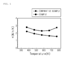
- a part of the composed materials prepared above was formed into a disk having a diameter of 10 mm and a thickness of 1 mm. After that, a pressure of 200 MPa was applied thereto by using a CIP (Cold Isostatic Pressing). Subsequently, the obtained result was put into a quartz tube and vacuum-sintered for 12 hours. In regard to the sintered disk, thermal conductivity was measured by using LFA457 (Netzsch, Inc) at predetermined temperature intervals. The measurement result is shown in FIG. 1 as Example.
- Co and Sb were prepared as reagents, and were mixed by using mortar to make a mixture having compositions of In 0.25 Co 4 Sb 12 in a pellet form.
- the mixture was heated at 500°C for 15 hours under H 2 (1.94%) and N 2 gas.
- the time for raising the temperature to 500°C was 1 hour and 30 minutes.
- the materials mixed as above were put in a silica tube and vacuum-sealed, and then were heated at 650°C for 36 hours.
- the time for raising the temperature to 650°C was 1 hour and 30 minutes, and In 0.25 Co 4 Sb 12 powder was obtained.
- a part of the material prepared above was formed into a disk having a diameter of 10 mm and a thickness of 1 mm. After that, a pressure of 200 MPa was applied thereto by using a CIP. Subsequently, the obtained result was put into a quartz tube and vacuum-sintered for 12 hours.
- thermal conductivity ( ⁇ ) was measured by using LFA457 (Netzsch, Inc). The measurement result is shown in FIG. 1 as Comparative Example.
- the compound semiconductor according to the Example of the present disclosure expressed by In 0.25 Co 4 Sb 10.6 0 0.4 Te has very low thermal conductivity ( ⁇ ) over the entire temperature measurement region in comparison to the compound semiconductor according to the Comparative Example expressed by In 0.25 Co 4 Sb 12 .
- the difference in thermal conductivity between the Example and the Comparative Example was greater in a high-temperature region.
- ZT ⁇ S 2 ⁇ T / K
- ⁇ electric conductivity
- S a Seebeck coefficient
- T temperature
- ⁇ thermal conductivity
- the compound semiconductor according to the present disclosure may have an improved ZT value since the thermal conductivity is low. Therefore, the compound semiconductor according to the present disclosure may be regarded as having excellent thermoelectric conversion and so can be very useful as a thermoelectric conversion material.
Landscapes
- Chemical & Material Sciences (AREA)
- Organic Chemistry (AREA)
- Inorganic Chemistry (AREA)
- Photovoltaic Devices (AREA)
- Inorganic Compounds Of Heavy Metals (AREA)
- Powder Metallurgy (AREA)
Abstract
Description
- The present disclosure relates to a new compound semiconductor material which may be used for solar cells or as thermoelectric materials, its preparation method, and its applications.
- This application claims priority to Korean Patent Application No.
10-2011-0045348 filed on May 13, 2011 10-2011-0045349 filed on May 13, 2011 10-2011-0049609 10-2012-0050459 filed on May 11, 2012 - A compound semiconductor is not a single element such as silicon and germanium but a compound having two or more kinds of combined elements serving as a semiconductor. Various kinds of compound semiconductors have been developed and used in many fields. For example, a compound semiconductor may be used for thermoelectric conversion devices using a Peltier effect, light emitting devices such as light emitting diodes and laser diodes using a photoelectric conversion effect, solar cells, or the like.
- Among these, the thermoelectric conversion device may be applied to thermoelectric conversion generation, thermoelectric conversion cooling or the like. Here, in the thermoelectric conversion generation, a thermal electromotive force generated by applying a temperature difference to the thermoelectric conversion device is used for converting thermal energy to electric energy.
- The energy conversion efficiency of the thermoelectric conversion device depends on ZT which is a performance index of the thermoelectric conversion material. Here, ZT is determined according to a Seebeck coefficient, electric conductivity, thermal conductivity, or the like. In more detail, ZT is proportional to the square of the Seebeck coefficient and the electric conductivity and is inversely proportional to the thermal conductivity. Therefore, in order to enhance the energy conversion efficiency of the thermoelectric conversion device, development of a thermoelectric conversion material with a high Seebeck coefficient, a high electric conductivity, or a low thermal conductivity is desired.
- Meanwhile, a solar cell is environment-friendly since it does not need an energy source other than solar rays, and therefore are actively studied as an alternative future energy source. A solar cell may be generally classified as a silicon solar cell using a single element of silicon, a compound semiconductor solar cell using a compound semiconductor, and a tandem solar cell where at least two solar cells having different band gap energies are stacked.
- Among these, a compound semiconductor solar cell uses a compound semiconductor in a light absorption layer which absorbs solar rays and generates an electron-hole pair, and may particularly use compound semiconductors in the III-V group such as GaAs, InP, GaAlAs and GaInAs, compound semiconductors in the II-VI group such as CdS, CdTe and ZnS, and compound semiconductors in the I-III-VI group represented by CuInSe2.
- The light absorption layer of the solar cell demands excellent long-term electric and optical stability, high photoelectric conversion efficiency, and easy control of the band gap energy or conductivity by composition change or doping. In addition, conditions such as production cost and yield should also be met for practical use. However, many conventional compound semiconductors fail to meet all of these conditions at once.
- The present disclosure is designed to solve the problems of the prior art, and therefore it is an object of the present disclosure to provide a new compound semiconductor material, which may be utilized in various ways for thermoelectric conversion materials of thermoelectric conversion devices, solar cells or the like, a preparation method thereof, and a thermoelectric conversion device or solar cell using the same.
- Other objects and advantages of the present disclosure will be understood from the following descriptions and become apparent by the embodiments of the present disclosure. In addition, it is understood that the objects and advantages of the present disclosure may be implemented by components defined in the appended claims or their combinations.
- In one aspect, after repeated studies of a compound semiconductor, inventors of the present disclosure have successfully synthesized a compound semiconductor represented by Chemical Formula 1, and found that this compound can be used for a thermoelectric conversion material of a thermoelectric conversion device or a light absorption layer of a solar cell.
Chemical Formula 1 InxCO4Sb12-n-zQ'nTez
- In the
Chemical Formula 1, Q' is at least one selected from the group consisting of O, S and Se, 0<x<0.5, 0<n≥2 and 0<z≥2. - Preferably, in
Chemical Formula - More preferably, in Chemical Formula 1, 0<x≤0.25.
- In another aspect, the present disclosure also provides a preparation method of a compound semiconductor, which includes: mixing In, Co, Sb and Te as well as at least one selected from the group consisting of O, S, Se and their oxides; and thermally treating the mixture.
- Preferably, the thermally treating step is performed at 400°C to 800°C.
- Also preferably, the thermally treating step includes at least two thermal treatment stages.
- In another aspect, the present disclosure also provides a thermoelectric conversion device, which includes the compound semiconductor as above.
- In another aspect, the present disclosure also provides a solar cell, which includes the compound semiconductor as above.
- According to the present disclosure, a new compound semiconductor material is provided.
- In one aspect, the new compound semiconductor may replace a conventional compound semiconductor or may be used as another material in addition to the conventional compound semiconductor.
- Further, in one aspect of the present disclosure, since the compound semiconductor has good thermoelectric conversion performance, it may be used for a thermoelectric conversion device. In particular, the compound semiconductor according to the present disclosure may have an improved ZT value which is a thermoelectric performance index, due to the improved thermal conductivity characteristic. Therefore, the compound semiconductor according to the present disclosure may be used as a thermoelectric conversion material of a thermoelectric conversion device.
- In addition, in another aspect of the present disclosure, the compound semiconductor may be used for a solar cell. Particularly, the compound semiconductor of the present disclosure may be used as a light absorption layer of the solar cell.
- Moreover, in another aspect of the present disclosure, the compound semiconductor may be used for an IR window or IR sensor which selectively passes IR, a magnetic device, a memory or the like.
- Other objects and aspects of the present disclosure will become apparent from the following descriptions of the embodiments with reference to the accompanying drawing in which:
-
FIG. 1 is a graph showing thermal conductivity values according to a temperature change of compound semiconductors according to an example according to the present disclosure and a comparative example. - Hereinafter, preferred embodiments of the present disclosure will be described in detail with reference to the accompanying drawings. Prior to the description, it should be understood that the terms used in the specification and the appended claims should not be construed as limited to general and dictionary meanings, but interpreted based on the meanings and concepts corresponding to technical aspects of the present disclosure based on the principle that the inventor is allowed to define terms.
- Therefore, the description proposed herein is just a preferable example for the purpose of illustration only, and is not intended to limit the scope of the disclosure, so it should be understood that other equivalents and modifications could be made thereto without departing from the spirit and scope of the disclosure.
- The present disclosure provides a new compound semiconductor represented by Chemical Formula 1 below.
Chemical Formula 1 InxCo4Sb12-n-zQ' nTez
- In the
Chemical Formula 1, Q' is at least one selected from the group consisting of O, S and Se. - In addition, in the Chemical Formula 1, 0<x<0.5, 0<n≤2 and 0<z≥2.
- Preferably, in
Chemical Formula - More preferably, in Chemical Formula 1, 0<x≤0.25.
- Also preferably, in Chemical Formula 1, 0<n+z≤3.
- Meanwhile, the compound semiconductor represented by Chemical Formula 1 may include a secondary phase partially, and the amount of the secondary phase may vary depending on a thermal treatment condition.
- The above compound semiconductor may be prepared by mixing In, Co, Sb and Te as well as at least one selected from the group consisting of O, S, Se and their oxides; and thermally treating the mixture.
- Meanwhile, each material used in the mixture forming step may be in a powder form, but the present disclosure is not limited to a specific form of the material.
- Preferably, the thermally treating step may be performed in vacuum or in a gas such as Ar, He and N2, partially containing hydrogen or not containing hydrogen.
- At this time, the thermally treating temperature may be 400°C to 800°C. Preferably, the thermally treating temperature may be 450°C to 700°C. More preferably, the thermally treating temperature may be 500°C to 650°C.
- Meanwhile, the thermally treating step may include at least two thermal treatment stages. For example, a first thermal treatment may be performed at a first temperature to the mixture obtained in the mixture forming step, namely in the step of mixing materials, and a second thermal treatment may be performed thereto at a second temperature.
- Here, some of the thermal treatment stages may be performed during the mixture forming step where materials are mixed is executed.
- For example, the thermally treating step may include three thermal treatment stages composed of a first thermal treatment stage, a second thermal treatment stage and a third thermal treatment (sintering) stage. In addition, the first thermal treatment stage may be performed in a temperature range of 400°C to 600°C, and the second and third thermal treatment stages may be performed in a temperature range of 600°C to 800°C. The first thermal treatment stage may be performed during the mixture forming step, and the second and third thermal treatment stages may be performed in order after the mixture forming step.
- A thermoelectric conversion device according to the present disclosure may include the compound semiconductor described above. In other words, the compound semiconductor according to the present disclosure may be used as a thermoelectric conversion material for the thermoelectric conversion device. Particularly, the compound semiconductor according to the present disclosure has a large ZT value, which is a performance index of the thermoelectric conversion material. In addition, due to low thermal conductivity, a high Seebeck coefficient and high electric conductivity, the compound semiconductor has excellent thermoelectric conversion performance. Therefore, the compound semiconductor according to the present disclosure may replace a conventional thermoelectric conversion material or may be used for a thermoelectric conversion device in addition to the conventional compound semiconductor.
- In addition, a solar cell according to the present disclosure may include the compound semiconductor above. In other words, the compound semiconductor according to the present disclosure may be used for a solar cell, particularly as a light absorption layer of the solar cell.
- The solar cell may be produced in a structure where a front surface transparent electrode, a buffer layer, a light absorption layer, a rear surface electrode and a substrate are laminated in order from the side where a solar ray is incident. The substrate located at the lowest portion may be made of glass, and the rear surface electrode on the entire surface thereof may be formed by depositing metal such as Mo.
- Subsequently, the compound semiconductor according to the present disclosure may be laminated on the rear surface electrode by means of an electron beam deposition method, a sol-gel method, or a PLD (Pulsed Laser Deposition) to form the light absorption layer. On the light absorption layer, a buffer layer for buffering the difference in lattice constants and band gaps between a ZnO layer serving as the front surface transparent electrode and the light absorption layer may be present. The buffer layer may be formed by depositing a material such as CdS by means of CBD (Chemical Bath Deposition) or the like. Next, the front surface transparent electrode may be formed on the buffer layer by means of sputtering or the like as a ZnO film or a ZnO and ITO laminate.
- The solar cell according to the present disclosure may be modified in various ways. For example, it is possible to manufacture a tandem solar cell where a solar cell using the compound semiconductor according to the present disclosure as the light absorption layer is laminated. In addition, the solar cell laminated as described above may employ a solar cell using silicon or another known compound semiconductor.
- In addition, it is possible to change a band gap of the compound semiconductor according to the present disclosure and laminate a plurality of solar cells which use compound semiconductors having different band gaps as the light absorption layer. The band gap of the compound semiconductor according to the present disclosure may be adjusted by changing a composition ratio of a component of the compound, particularly Te.
- In addition, the compound semiconductor according to the present disclosure may also be applied to IR windows or IR sensors which selectively pass IR.
- Hereinafter, embodiments of the present disclosure will be described in detail. The embodiments of the present disclosure, however, may take several other forms, and the scope of the present disclosure should not be construed as being limited to the following examples. The embodiments of the present disclosure are provided to more fully explain the present disclosure to those having ordinary knowledge in the art to which the present disclosure pertains.
- 0.0510g of In, 0.3873g of Co, 2.2923g of Sb, 0.0428g of Co3O4 and 127.6g of Te were prepared as reagents, and were mixed by using mortar. The materials mixed as above were put into a silica tube and vacuum-sealed and then heated at 650°C for 36 hours. The time for raising the temperature to 650°C was 1 hour and 30 minutes, and In0.25Co4Sb10.6O0.4Te powder was obtained.
- A part of the composed materials prepared above was formed into a disk having a diameter of 10 mm and a thickness of 1 mm. After that, a pressure of 200 MPa was applied thereto by using a CIP (Cold Isostatic Pressing). Subsequently, the obtained result was put into a quartz tube and vacuum-sintered for 12 hours. In regard to the sintered disk, thermal conductivity was measured by using LFA457 (Netzsch, Inc) at predetermined temperature intervals. The measurement result is shown in
FIG. 1 as Example. - In, Co and Sb were prepared as reagents, and were mixed by using mortar to make a mixture having compositions of In0.25Co4Sb12 in a pellet form. The mixture was heated at 500°C for 15 hours under H2 (1.94%) and N2 gas. The time for raising the temperature to 500°C was 1 hour and 30 minutes.
- The materials mixed as above were put in a silica tube and vacuum-sealed, and then were heated at 650°C for 36 hours. The time for raising the temperature to 650°C was 1 hour and 30 minutes, and In0.25Co4Sb12 powder was obtained.
- A part of the material prepared above was formed into a disk having a diameter of 10 mm and a thickness of 1 mm. After that, a pressure of 200 MPa was applied thereto by using a CIP. Subsequently, the obtained result was put into a quartz tube and vacuum-sintered for 12 hours.
- In regard to the sintered disk, thermal conductivity (κ) was measured by using LFA457 (Netzsch, Inc). The measurement result is shown in
FIG. 1 as Comparative Example. - Referring to the results shown in
FIG. 1 , it could be found that the compound semiconductor according to the Example of the present disclosure expressed by In0.25Co4Sb10.600.4Te has very low thermal conductivity (κ) over the entire temperature measurement region in comparison to the compound semiconductor according to the Comparative Example expressed by In0.25Co4Sb12. In particular, it could be found that the difference in thermal conductivity between the Example and the Comparative Example was greater in a high-temperature region. - In addition, the ZT value which is a thermoelectric performance index can be expressed as follows:

- Here, σ represents electric conductivity, S represents a Seebeck coefficient, T represents temperature, and κ represents thermal conductivity
- The compound semiconductor according to the present disclosure may have an improved ZT value since the thermal conductivity is low. Therefore, the compound semiconductor according to the present disclosure may be regarded as having excellent thermoelectric conversion and so can be very useful as a thermoelectric conversion material.
- The present disclosure has been described in detail. However, it should be understood that the detailed description and specific examples, while indicating preferred embodiments of the disclosure, are given by way of illustration only, since various changes and modifications within the spirit and scope of the disclosure will become apparent to those skilled in the art from this detailed description.
Claims (9)
- A compound semiconductor, represented by Chemical Formula 1 below:
Chemical Formula 1 InxCo4Sb12-n-zQ'nTez
where, in the Chemical Formula 1, Q' is at least one selected from the group consisting of O, S and Se, 0<x<0.5, 0<n≥2 and 0<z≥2. - The compound semiconductor according to claim 1, wherein, in Chemical Formula 1, 0<x≥0.4.
- The compound semiconductor according to claim 1, wherein, in Chemical Formula 1, 0<x≤0.25.
- The compound semiconductor according to claim 1, wherein, in Chemical Formula 1, 0<n+z≤3.
- A preparation method of a compound semiconductor, comprising:forming a mixture containing In, Co, Sb and Te as well as at least one selected from the group consisting of O, S, Se and their oxides; andthermally treating the mixture, thereby preparing the compound semiconductor defined in claim 1.
- The preparation method of a compound semiconductor according to claim 5, wherein the thermally treating step is performed at 400°C to 800°C.
- The preparation method of a compound semiconductor according to claim 5, wherein the thermally treating step includes at least two thermal treatment stages.
- A thermoelectric conversion device, which includes the compound semiconductor defined in any one of claims 1 to 4.
- A solar cell, which includes the compound semiconductor defined in any one of claims 1 to 3.
Applications Claiming Priority (5)
| Application Number | Priority Date | Filing Date | Title |
|---|---|---|---|
| KR20110045348 | 2011-05-13 | ||
| KR20110045349 | 2011-05-13 | ||
| KR20110049609 | 2011-05-25 | ||
| PCT/KR2012/003738 WO2012157915A1 (en) | 2011-05-13 | 2012-05-11 | Novel compound semiconductor and usage for same |
| KR1020120050459A KR101453036B1 (en) | 2011-05-13 | 2012-05-11 | New compound semiconductors and their application |
Publications (3)
| Publication Number | Publication Date |
|---|---|
| EP2708503A1 true EP2708503A1 (en) | 2014-03-19 |
| EP2708503A4 EP2708503A4 (en) | 2015-04-01 |
| EP2708503B1 EP2708503B1 (en) | 2017-02-15 |
Family
ID=47177151
Family Applications (1)
| Application Number | Title | Priority Date | Filing Date |
|---|---|---|---|
| EP12786280.3A Active EP2708503B1 (en) | 2011-05-13 | 2012-05-11 | Novel compound semiconductor and usage for same |
Country Status (7)
| Country | Link |
|---|---|
| US (1) | US8636925B2 (en) |
| EP (1) | EP2708503B1 (en) |
| JP (1) | JP5774201B2 (en) |
| KR (1) | KR101453036B1 (en) |
| CN (1) | CN103517872B (en) |
| TW (1) | TWI469931B (en) |
| WO (1) | WO2012157915A1 (en) |
Families Citing this family (4)
| Publication number | Priority date | Publication date | Assignee | Title |
|---|---|---|---|---|
| CN103562127B (en) * | 2011-05-13 | 2016-07-13 | Lg化学株式会社 | New compound semiconductor and application thereof |
| JP5767399B2 (en) * | 2011-05-13 | 2015-08-19 | エルジー・ケム・リミテッド | New compound semiconductors and their utilization |
| KR102122573B1 (en) * | 2017-03-09 | 2020-06-12 | 주식회사 엘지화학 | Compound semiconductors and their application |
| CA3241652A1 (en) * | 2022-02-25 | 2023-08-31 | Jerald A. Trepanier | Communication system for patient support apparatuses and temperature management devices |
Family Cites Families (20)
| Publication number | Priority date | Publication date | Assignee | Title |
|---|---|---|---|---|
| JPH01298010A (en) * | 1988-05-26 | 1989-12-01 | Mitsubishi Metal Corp | Production of metal selenide |
| JPH02199006A (en) * | 1989-01-30 | 1990-08-07 | Agency Of Ind Science & Technol | Multielement-based metal chalocogenide having 1/2/5 composition |
| JP2002270907A (en) * | 2001-03-06 | 2002-09-20 | Nec Corp | Thermoelectric conversion material and device using the same |
| EP1665401A2 (en) * | 2003-09-12 | 2006-06-07 | Board of Trustees operating Michigan State University | Silver-containing thermoelectric compounds |
| JP2005116746A (en) * | 2003-10-07 | 2005-04-28 | Toshiba Corp | Thermoelectric conversion material and thermoelectric conversion element using the same |
| US7462217B2 (en) * | 2003-12-08 | 2008-12-09 | E.I. Du Pont De Nemours And Company | Method of preparation for the high performance thermoelectric material indium-cobalt-antimony |
| JP2008500451A (en) * | 2004-04-14 | 2008-01-10 | イー・アイ・デュポン・ドウ・ヌムール・アンド・カンパニー | High performance thermoelectric materials and methods for their preparation |
| JP5055747B2 (en) * | 2004-11-10 | 2012-10-24 | 大日本印刷株式会社 | Method for producing metal oxide film |
| US8329319B2 (en) * | 2005-10-17 | 2012-12-11 | Agency For Science, Technology And Research | Phase change magnetic material |
| AU2007217870B2 (en) * | 2006-02-16 | 2011-07-21 | Brigham Young University | Preparation of uniform nanoparticles of ultra-high purity metal oxides, mixed metal oxides, metals, and metal alloys |
| JP5028616B2 (en) * | 2006-08-03 | 2012-09-19 | 国立大学法人宇都宮大学 | Method for producing metal sulfide |
| JP5205904B2 (en) * | 2006-09-29 | 2013-06-05 | 大日本印刷株式会社 | Method for producing metal oxide film and laminate |
| KR100910173B1 (en) * | 2007-09-10 | 2009-07-30 | 충주대학교 산학협력단 | COSP3 Scutterudite thermoelectric material and its manufacturing method |
| US10508324B2 (en) * | 2008-01-23 | 2019-12-17 | Furukawa Co., Ltd. | Thermoelectric conversion material and thermoelectric conversion module |
| JP2009253301A (en) * | 2008-04-04 | 2009-10-29 | Samsung Electronics Co Ltd | Dichalcogenide thermoelectric material |
| EP2319082B1 (en) * | 2008-08-29 | 2017-11-15 | LG Chem, Ltd. | New compound semiconductor and producing method thereof, and solar cell and thermoelectric conversion element using the same |
| CN101397612B (en) * | 2008-10-21 | 2011-05-25 | 同济大学 | A kind of preparation method of skutterudite-based thermoelectric block material |
| KR101042575B1 (en) * | 2009-08-11 | 2011-06-20 | 충주대학교 산학협력단 | INC-FE-SC-based scrutherite thermoelectric material and its manufacturing method |
| KR101042574B1 (en) * | 2009-08-11 | 2011-06-20 | 충주대학교 산학협력단 | INC-Ni-S-based scrutherite thermoelectric material and its manufacturing method |
| JP5767399B2 (en) * | 2011-05-13 | 2015-08-19 | エルジー・ケム・リミテッド | New compound semiconductors and their utilization |
-
2012
- 2012-05-11 JP JP2014506350A patent/JP5774201B2/en active Active
- 2012-05-11 KR KR1020120050459A patent/KR101453036B1/en active Active
- 2012-05-11 CN CN201280022977.2A patent/CN103517872B/en active Active
- 2012-05-11 WO PCT/KR2012/003738 patent/WO2012157915A1/en not_active Ceased
- 2012-05-11 EP EP12786280.3A patent/EP2708503B1/en active Active
- 2012-05-14 TW TW101117052A patent/TWI469931B/en active
- 2012-09-14 US US13/616,679 patent/US8636925B2/en active Active
Also Published As
| Publication number | Publication date |
|---|---|
| KR101453036B1 (en) | 2014-10-22 |
| WO2012157915A1 (en) | 2012-11-22 |
| KR20120127321A (en) | 2012-11-21 |
| US20130009106A1 (en) | 2013-01-10 |
| CN103517872A (en) | 2014-01-15 |
| CN103517872B (en) | 2015-08-05 |
| TW201305061A (en) | 2013-02-01 |
| EP2708503B1 (en) | 2017-02-15 |
| JP2014519547A (en) | 2014-08-14 |
| EP2708503A4 (en) | 2015-04-01 |
| US8636925B2 (en) | 2014-01-28 |
| JP5774201B2 (en) | 2015-09-09 |
| TWI469931B (en) | 2015-01-21 |
Similar Documents
| Publication | Publication Date | Title |
|---|---|---|
| EP2708505A1 (en) | Novel compound semiconductor and usage for same | |
| US8747704B2 (en) | Compound semiconductors and their application | |
| EP2708495B1 (en) | New compound semiconductors and their application | |
| US8703024B2 (en) | Compound semiconductors and their application | |
| EP2703344B1 (en) | Novel compound semiconductor and use thereof | |
| EP2708502B1 (en) | Novel compound semiconductor and usage for same | |
| EP2708496B1 (en) | Novel compound semiconductor and usage for same | |
| EP2708501B1 (en) | Novel compound semiconductor and usage for same | |
| US8603368B2 (en) | Compound semiconductors and their application | |
| US8636925B2 (en) | Compound semiconductors and their application | |
| EP2708499B1 (en) | New compound semiconductors and their application | |
| EP2708500B1 (en) | Novel compound semiconductor and usage for same | |
| US8747705B2 (en) | Compound semiconductors and their application | |
| EP2708504B1 (en) | Novel compound semiconductor and usage for same |
Legal Events
| Date | Code | Title | Description |
|---|---|---|---|
| PUAI | Public reference made under article 153(3) epc to a published international application that has entered the european phase |
Free format text: ORIGINAL CODE: 0009012 |
|
| 17P | Request for examination filed |
Effective date: 20131024 |
|
| AK | Designated contracting states |
Kind code of ref document: A1 Designated state(s): AL AT BE BG CH CY CZ DE DK EE ES FI FR GB GR HR HU IE IS IT LI LT LU LV MC MK MT NL NO PL PT RO RS SE SI SK SM TR |
|
| DAX | Request for extension of the european patent (deleted) | ||
| REG | Reference to a national code |
Ref country code: DE Ref legal event code: R079 Ref document number: 602012028731 Country of ref document: DE Free format text: PREVIOUS MAIN CLASS: C01B0019000000 Ipc: C01G0051000000 |
|
| RA4 | Supplementary search report drawn up and despatched (corrected) |
Effective date: 20150304 |
|
| RIC1 | Information provided on ipc code assigned before grant |
Ipc: H01L 35/18 20060101ALI20150226BHEP Ipc: C01G 51/00 20060101AFI20150226BHEP Ipc: C01B 19/00 20060101ALI20150226BHEP |
|
| GRAP | Despatch of communication of intention to grant a patent |
Free format text: ORIGINAL CODE: EPIDOSNIGR1 |
|
| STAA | Information on the status of an ep patent application or granted ep patent |
Free format text: STATUS: GRANT OF PATENT IS INTENDED |
|
| INTG | Intention to grant announced |
Effective date: 20161129 |
|
| GRAS | Grant fee paid |
Free format text: ORIGINAL CODE: EPIDOSNIGR3 |
|
| GRAA | (expected) grant |
Free format text: ORIGINAL CODE: 0009210 |
|
| STAA | Information on the status of an ep patent application or granted ep patent |
Free format text: STATUS: THE PATENT HAS BEEN GRANTED |
|
| AK | Designated contracting states |
Kind code of ref document: B1 Designated state(s): AL AT BE BG CH CY CZ DE DK EE ES FI FR GB GR HR HU IE IS IT LI LT LU LV MC MK MT NL NO PL PT RO RS SE SI SK SM TR |
|
| REG | Reference to a national code |
Ref country code: CH Ref legal event code: EP Ref country code: GB Ref legal event code: FG4D |
|
| REG | Reference to a national code |
Ref country code: IE Ref legal event code: FG4D |
|
| REG | Reference to a national code |
Ref country code: AT Ref legal event code: REF Ref document number: 867782 Country of ref document: AT Kind code of ref document: T Effective date: 20170315 |
|
| REG | Reference to a national code |
Ref country code: DE Ref legal event code: R096 Ref document number: 602012028731 Country of ref document: DE |
|
| REG | Reference to a national code |
Ref country code: FR Ref legal event code: PLFP Year of fee payment: 6 |
|
| REG | Reference to a national code |
Ref country code: NL Ref legal event code: MP Effective date: 20170215 |
|
| REG | Reference to a national code |
Ref country code: LT Ref legal event code: MG4D |
|
| REG | Reference to a national code |
Ref country code: AT Ref legal event code: MK05 Ref document number: 867782 Country of ref document: AT Kind code of ref document: T Effective date: 20170215 |
|
| PG25 | Lapsed in a contracting state [announced via postgrant information from national office to epo] |
Ref country code: HR Free format text: LAPSE BECAUSE OF FAILURE TO SUBMIT A TRANSLATION OF THE DESCRIPTION OR TO PAY THE FEE WITHIN THE PRESCRIBED TIME-LIMIT Effective date: 20170215 Ref country code: LT Free format text: LAPSE BECAUSE OF FAILURE TO SUBMIT A TRANSLATION OF THE DESCRIPTION OR TO PAY THE FEE WITHIN THE PRESCRIBED TIME-LIMIT Effective date: 20170215 Ref country code: FI Free format text: LAPSE BECAUSE OF FAILURE TO SUBMIT A TRANSLATION OF THE DESCRIPTION OR TO PAY THE FEE WITHIN THE PRESCRIBED TIME-LIMIT Effective date: 20170215 Ref country code: GR Free format text: LAPSE BECAUSE OF FAILURE TO SUBMIT A TRANSLATION OF THE DESCRIPTION OR TO PAY THE FEE WITHIN THE PRESCRIBED TIME-LIMIT Effective date: 20170516 Ref country code: NO Free format text: LAPSE BECAUSE OF FAILURE TO SUBMIT A TRANSLATION OF THE DESCRIPTION OR TO PAY THE FEE WITHIN THE PRESCRIBED TIME-LIMIT Effective date: 20170515 |
|
| PG25 | Lapsed in a contracting state [announced via postgrant information from national office to epo] |
Ref country code: AT Free format text: LAPSE BECAUSE OF FAILURE TO SUBMIT A TRANSLATION OF THE DESCRIPTION OR TO PAY THE FEE WITHIN THE PRESCRIBED TIME-LIMIT Effective date: 20170215 Ref country code: ES Free format text: LAPSE BECAUSE OF FAILURE TO SUBMIT A TRANSLATION OF THE DESCRIPTION OR TO PAY THE FEE WITHIN THE PRESCRIBED TIME-LIMIT Effective date: 20170215 Ref country code: RS Free format text: LAPSE BECAUSE OF FAILURE TO SUBMIT A TRANSLATION OF THE DESCRIPTION OR TO PAY THE FEE WITHIN THE PRESCRIBED TIME-LIMIT Effective date: 20170215 Ref country code: PT Free format text: LAPSE BECAUSE OF FAILURE TO SUBMIT A TRANSLATION OF THE DESCRIPTION OR TO PAY THE FEE WITHIN THE PRESCRIBED TIME-LIMIT Effective date: 20170615 Ref country code: SE Free format text: LAPSE BECAUSE OF FAILURE TO SUBMIT A TRANSLATION OF THE DESCRIPTION OR TO PAY THE FEE WITHIN THE PRESCRIBED TIME-LIMIT Effective date: 20170215 Ref country code: BG Free format text: LAPSE BECAUSE OF FAILURE TO SUBMIT A TRANSLATION OF THE DESCRIPTION OR TO PAY THE FEE WITHIN THE PRESCRIBED TIME-LIMIT Effective date: 20170515 Ref country code: LU Free format text: LAPSE BECAUSE OF NON-PAYMENT OF DUE FEES Effective date: 20170531 Ref country code: LV Free format text: LAPSE BECAUSE OF FAILURE TO SUBMIT A TRANSLATION OF THE DESCRIPTION OR TO PAY THE FEE WITHIN THE PRESCRIBED TIME-LIMIT Effective date: 20170215 Ref country code: NL Free format text: LAPSE BECAUSE OF FAILURE TO SUBMIT A TRANSLATION OF THE DESCRIPTION OR TO PAY THE FEE WITHIN THE PRESCRIBED TIME-LIMIT Effective date: 20170215 |
|
| PG25 | Lapsed in a contracting state [announced via postgrant information from national office to epo] |
Ref country code: CZ Free format text: LAPSE BECAUSE OF FAILURE TO SUBMIT A TRANSLATION OF THE DESCRIPTION OR TO PAY THE FEE WITHIN THE PRESCRIBED TIME-LIMIT Effective date: 20170215 Ref country code: RO Free format text: LAPSE BECAUSE OF FAILURE TO SUBMIT A TRANSLATION OF THE DESCRIPTION OR TO PAY THE FEE WITHIN THE PRESCRIBED TIME-LIMIT Effective date: 20170215 Ref country code: IT Free format text: LAPSE BECAUSE OF FAILURE TO SUBMIT A TRANSLATION OF THE DESCRIPTION OR TO PAY THE FEE WITHIN THE PRESCRIBED TIME-LIMIT Effective date: 20170215 Ref country code: SK Free format text: LAPSE BECAUSE OF FAILURE TO SUBMIT A TRANSLATION OF THE DESCRIPTION OR TO PAY THE FEE WITHIN THE PRESCRIBED TIME-LIMIT Effective date: 20170215 Ref country code: EE Free format text: LAPSE BECAUSE OF FAILURE TO SUBMIT A TRANSLATION OF THE DESCRIPTION OR TO PAY THE FEE WITHIN THE PRESCRIBED TIME-LIMIT Effective date: 20170215 |
|
| REG | Reference to a national code |
Ref country code: DE Ref legal event code: R097 Ref document number: 602012028731 Country of ref document: DE |
|
| PG25 | Lapsed in a contracting state [announced via postgrant information from national office to epo] |
Ref country code: PL Free format text: LAPSE BECAUSE OF FAILURE TO SUBMIT A TRANSLATION OF THE DESCRIPTION OR TO PAY THE FEE WITHIN THE PRESCRIBED TIME-LIMIT Effective date: 20170215 Ref country code: SM Free format text: LAPSE BECAUSE OF FAILURE TO SUBMIT A TRANSLATION OF THE DESCRIPTION OR TO PAY THE FEE WITHIN THE PRESCRIBED TIME-LIMIT Effective date: 20170215 Ref country code: DK Free format text: LAPSE BECAUSE OF FAILURE TO SUBMIT A TRANSLATION OF THE DESCRIPTION OR TO PAY THE FEE WITHIN THE PRESCRIBED TIME-LIMIT Effective date: 20170215 |
|
| PLBE | No opposition filed within time limit |
Free format text: ORIGINAL CODE: 0009261 |
|
| STAA | Information on the status of an ep patent application or granted ep patent |
Free format text: STATUS: NO OPPOSITION FILED WITHIN TIME LIMIT |
|
| REG | Reference to a national code |
Ref country code: CH Ref legal event code: PL |
|
| 26N | No opposition filed |
Effective date: 20171116 |
|
| PG25 | Lapsed in a contracting state [announced via postgrant information from national office to epo] |
Ref country code: MC Free format text: LAPSE BECAUSE OF FAILURE TO SUBMIT A TRANSLATION OF THE DESCRIPTION OR TO PAY THE FEE WITHIN THE PRESCRIBED TIME-LIMIT Effective date: 20170215 |
|
| REG | Reference to a national code |
Ref country code: IE Ref legal event code: MM4A |
|
| PG25 | Lapsed in a contracting state [announced via postgrant information from national office to epo] |
Ref country code: SI Free format text: LAPSE BECAUSE OF FAILURE TO SUBMIT A TRANSLATION OF THE DESCRIPTION OR TO PAY THE FEE WITHIN THE PRESCRIBED TIME-LIMIT Effective date: 20170215 Ref country code: LI Free format text: LAPSE BECAUSE OF NON-PAYMENT OF DUE FEES Effective date: 20170531 Ref country code: CH Free format text: LAPSE BECAUSE OF NON-PAYMENT OF DUE FEES Effective date: 20170531 |
|
| PG25 | Lapsed in a contracting state [announced via postgrant information from national office to epo] |
Ref country code: LU Free format text: LAPSE BECAUSE OF NON-PAYMENT OF DUE FEES Effective date: 20170511 |
|
| REG | Reference to a national code |
Ref country code: FR Ref legal event code: PLFP Year of fee payment: 7 |
|
| REG | Reference to a national code |
Ref country code: BE Ref legal event code: MM Effective date: 20170531 |
|
| PG25 | Lapsed in a contracting state [announced via postgrant information from national office to epo] |
Ref country code: IE Free format text: LAPSE BECAUSE OF NON-PAYMENT OF DUE FEES Effective date: 20170511 |
|
| PG25 | Lapsed in a contracting state [announced via postgrant information from national office to epo] |
Ref country code: BE Free format text: LAPSE BECAUSE OF NON-PAYMENT OF DUE FEES Effective date: 20170531 |
|
| PG25 | Lapsed in a contracting state [announced via postgrant information from national office to epo] |
Ref country code: MT Free format text: LAPSE BECAUSE OF NON-PAYMENT OF DUE FEES Effective date: 20170511 |
|
| PG25 | Lapsed in a contracting state [announced via postgrant information from national office to epo] |
Ref country code: HU Free format text: LAPSE BECAUSE OF FAILURE TO SUBMIT A TRANSLATION OF THE DESCRIPTION OR TO PAY THE FEE WITHIN THE PRESCRIBED TIME-LIMIT; INVALID AB INITIO Effective date: 20120511 |
|
| PG25 | Lapsed in a contracting state [announced via postgrant information from national office to epo] |
Ref country code: CY Free format text: LAPSE BECAUSE OF NON-PAYMENT OF DUE FEES Effective date: 20170215 |
|
| PG25 | Lapsed in a contracting state [announced via postgrant information from national office to epo] |
Ref country code: MK Free format text: LAPSE BECAUSE OF FAILURE TO SUBMIT A TRANSLATION OF THE DESCRIPTION OR TO PAY THE FEE WITHIN THE PRESCRIBED TIME-LIMIT Effective date: 20170215 |
|
| PG25 | Lapsed in a contracting state [announced via postgrant information from national office to epo] |
Ref country code: TR Free format text: LAPSE BECAUSE OF FAILURE TO SUBMIT A TRANSLATION OF THE DESCRIPTION OR TO PAY THE FEE WITHIN THE PRESCRIBED TIME-LIMIT Effective date: 20170215 |
|
| PG25 | Lapsed in a contracting state [announced via postgrant information from national office to epo] |
Ref country code: AL Free format text: LAPSE BECAUSE OF FAILURE TO SUBMIT A TRANSLATION OF THE DESCRIPTION OR TO PAY THE FEE WITHIN THE PRESCRIBED TIME-LIMIT Effective date: 20170215 Ref country code: IS Free format text: LAPSE BECAUSE OF FAILURE TO SUBMIT A TRANSLATION OF THE DESCRIPTION OR TO PAY THE FEE WITHIN THE PRESCRIBED TIME-LIMIT Effective date: 20170615 |
|
| PGFP | Annual fee paid to national office [announced via postgrant information from national office to epo] |
Ref country code: DE Payment date: 20250422 Year of fee payment: 14 |
|
| PGFP | Annual fee paid to national office [announced via postgrant information from national office to epo] |
Ref country code: FR Payment date: 20250422 Year of fee payment: 14 |
|
| PGFP | Annual fee paid to national office [announced via postgrant information from national office to epo] |
Ref country code: GB Payment date: 20260324 Year of fee payment: 15 |