EP2707888B1 - Schaltvorrichtung - Google Patents
Schaltvorrichtung Download PDFInfo
- Publication number
- EP2707888B1 EP2707888B1 EP12726411.7A EP12726411A EP2707888B1 EP 2707888 B1 EP2707888 B1 EP 2707888B1 EP 12726411 A EP12726411 A EP 12726411A EP 2707888 B1 EP2707888 B1 EP 2707888B1
- Authority
- EP
- European Patent Office
- Prior art keywords
- switching
- switching device
- semiconductor
- arrangement
- electromechanical
- Prior art date
- Legal status (The legal status is an assumption and is not a legal conclusion. Google has not performed a legal analysis and makes no representation as to the accuracy of the status listed.)
- Active
Links
Images


Classifications
-
- H—ELECTRICITY
- H01—ELECTRIC ELEMENTS
- H01H—ELECTRIC SWITCHES; RELAYS; SELECTORS; EMERGENCY PROTECTIVE DEVICES
- H01H9/00—Details of switching devices, not covered by groups H01H1/00 - H01H7/00
- H01H9/54—Circuit arrangements not adapted to a particular application of the switching device and for which no provision exists elsewhere
- H01H9/541—Contacts shunted by semiconductor devices
-
- H—ELECTRICITY
- H01—ELECTRIC ELEMENTS
- H01H—ELECTRIC SWITCHES; RELAYS; SELECTORS; EMERGENCY PROTECTIVE DEVICES
- H01H33/00—High-tension or heavy-current switches with arc-extinguishing or arc-preventing means
- H01H33/02—Details
- H01H33/59—Circuit arrangements not adapted to a particular application of the switch and not otherwise provided for, e.g. for ensuring operation of the switch at a predetermined point in the AC cycle
- H01H33/596—Circuit arrangements not adapted to a particular application of the switch and not otherwise provided for, e.g. for ensuring operation of the switch at a predetermined point in the AC cycle for interrupting DC
-
- H—ELECTRICITY
- H02—GENERATION; CONVERSION OR DISTRIBUTION OF ELECTRIC POWER
- H02H—EMERGENCY PROTECTIVE CIRCUIT ARRANGEMENTS
- H02H3/00—Emergency protective circuit arrangements for automatic disconnection directly responsive to an undesired change from normal electric working condition with or without subsequent reconnection ; integrated protection
- H02H3/08—Emergency protective circuit arrangements for automatic disconnection directly responsive to an undesired change from normal electric working condition with or without subsequent reconnection ; integrated protection responsive to excess current
- H02H3/087—Emergency protective circuit arrangements for automatic disconnection directly responsive to an undesired change from normal electric working condition with or without subsequent reconnection ; integrated protection responsive to excess current for DC applications
-
- H—ELECTRICITY
- H02—GENERATION; CONVERSION OR DISTRIBUTION OF ELECTRIC POWER
- H02H—EMERGENCY PROTECTIVE CIRCUIT ARRANGEMENTS
- H02H3/00—Emergency protective circuit arrangements for automatic disconnection directly responsive to an undesired change from normal electric working condition with or without subsequent reconnection ; integrated protection
- H02H3/02—Details
- H02H3/025—Disconnection after limiting, e.g. when limiting is not sufficient or for facilitating disconnection
Definitions
- the invention relates to a switching device for switching bipolar DC currents in high-voltage networks.
- DC currents in high voltage networks can not be interrupted by means of known switching principles, which are based on the current zero crossing of the alternating current.
- Known concepts for switches for switching bipolar DC currents in high voltage networks rely on the use of components and subsystems used for the high voltage DC converter stations. These concepts have the disadvantage that the current flow takes place in the normal operating state through the turn-off semiconductor components and thus non-negligible power losses occur.
- the aforementioned elements are arranged so that the DC current in a first switching state of the switching device can be guided via at least one of the electromechanical switching units without flowing through the semiconductor switching arrangement. In a second switching state of the device, however, the current is feasible via the semiconductor switching arrangement.
- the construction according to the invention advantageously leads to a simpler, modular construction and associated reduced production costs. However, it is particularly advantageous that in the conducting state the current does not flow through semiconductor switches with considerable losses, but via the electromechanical switching unit.
- the semiconductor switching device may be designed so that it can conduct current in both directions or only in one direction. However, in order to keep the structure of the semiconductor switching device simple and thus the cost low, it is advantageous if the semiconductor switching device is designed only for current flow in one direction.
- the semiconductor switching device can in turn consist of a plurality of semiconductor cells which are capable of receiving a partial voltage of the DC high voltage. Each of these semiconductor cells in turn can be constructed according to known concepts such as the concept known as MMC circuit.
- the electromechanical switching units are expediently one or a combination of a plurality of switches, as used for switching alternating currents.
- this electromechanical switch can be used, the breaker and insulating properties based on the vacuum switching principle or a switching principle with a quenching and insulating.
- the switching device comprises a further electromechanical switching unit.
- the further electromechanical switching unit is connected as a connection of one of the connection points of the semiconductor switching arrangement to the other pole of the DC line.
- the switching device has four electromechanical switching units in full bridge arrangement or H-bridge arrangement.
- the semiconductor switching arrangement is suitably connected as a connection of the centers of the two bridge branches.
- the semiconductor switching arrangement preferably comprises a device for receiving the switching energy. As a result, the switching energy to be converted during the switch-off process can be reduced.
- At least one of the electromechanical switching units is opened.
- the switches contained in an electromechanical switching unit are expediently opened and the resulting arc voltage causes the current to commutate to the switched-on semiconductor switching arrangement. This results in a current zero crossing in the switching off electromechanical switching unit and thus to interrupt the flow of current in this electromechanical switching unit.
- electromechanical switching units are arranged in a bridge circuit, then one electromechanical switching unit of each bridge branch can be used to switch off the current, wherein the electromechanical switching unit is arranged in the first bridge branch in the current flow direction in front of the semiconductor switching device and the electromechanical switching unit of the other bridge branch in the current flow direction after the semiconductor switching device.
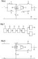
- FIG. 1 shows a first embodiment of the invention.
- first switching device 10 has a full bridge arrangement consisting of a first to fourth power switch 11 ... 14.
- the bridge circuit has in the usual way two parallel branches, in each of which two of the power switches 11 ... 14 are connected in series.
- the center between the first and second power switches 11, 12 is connected via a semiconductor switching device 15 to the middle between the third and fourth power switches 13, 14.
- Parallel to the semiconductor switching arrangement 15, an energy absorbing element 16 is provided.
- the semiconductor switching arrangement 15 in the present exemplary embodiment is a series connection of and known Modular Multilevel Converter (MMC) modules.
- MMC Modular Multilevel Converter
- the energy absorbing element 16 is a plurality of high voltage arresters.
- FIG. 1 shows in addition to the basic structure of the first switching device, this simultaneously in a first switching state, which corresponds to the normal operation in power line.
- a first switching state which corresponds to the normal operation in power line.
- all four power switches 11 ... 14 are closed.
- the current can flow unhindered over the two branches of the bridge arrangement.
- the power switches 11 ... 14 have a very low resistance.
- the semiconductor switching device 15 is substantially free of stress.
- FIG. 4 shows a first to fourth method step 41 to 44.
- the semiconductor switching device 15 is turned on. So it goes into the conductive state, but still does not carry any significant current, because it is not under tension.
- the second method step 42 the second power switch 12 and the third power switch 13 are now opened. With sufficient voltage drop across the switching paths of these power switches 12, 13, the current forcibly commutated in the semiconductor switching device 15 and the arcs in the circuit breakers 12, 13 are deleted. The circuit breakers 12, 13 insulate from this point on.
- the semiconductor switching arrangement 15 is switched off and the energy stored in the DC circuit is dissipated in the energy-absorbing element 16.
- the two other power switches 11, 14 open and thus disconnect the semiconductor switching arrangement 15 completely from the DC network.
- the power switches 11 ... 14 are turned on while the semiconductor switching device 15 remains inactive.
- FIG. 2 shows the state of the first switching device 10 after the second method step 42
- FIG. 3 shows the state of the first switching device 10 after the fourth method step 44.
- FIG. 5 shows the second switching device 50 in normal operation, ie with power line.
- the second switching device 50 has, similar to the first switching device 10, a full bridge of circuit breakers 11 ... 14. Furthermore, the second switching device 50 has a semiconductor switching arrangement 15, wherein the semiconductor switching arrangement 15 is connected as well as in the first switching device 10.
- the second switching device 50 has a further power switch 51.
- the further power switch 51 in this case connects a connection point of the semiconductor switching arrangement 15 with the pole which can not be switched off by the switching device 50, which in this case is the negative pole.
- a switching state is set in FIG. 5 is shown.
- the first and second power switches 11, 12 are closed.
- the third and fourth power switches 13, 14 are open when the power line.
- the further power switch 51 is closed.
- the entire mains voltage drops across both circuit breakers 13, 14, which is to be isolated by the two power switches 13, 14.
- the first two power switches 11, 12 carry the current and the semiconductor switching device 15 is under the full voltage.
- a supply voltage for driving the semiconductor switching device 15 is constantly available.
- the semiconductor switching device 15 is essentially no electricity, except for the electricity required to cover its own energy demand, since it is in a de-energized state. Thus, the losses are low.
- FIG. 7 shows a first to seventh shutdown step 71 to 77th
- the further power switch 51 is opened to disconnect the semiconductor switching device 15 from the negative pole. It is expedient to convert the semiconductor switching arrangement 15 into an off state so that it can build up the full mains voltage and the current through the semiconductor switching arrangement 15 becomes zero. Then, the opening of the further circuit breaker 51 can be carried out without current and voltage.
- the semiconductor switching arrangement 15 is activated in such a way that it becomes conductive and thus its terminal voltage becomes zero. This drops over the other circuit breaker 51, the full line voltage.
- the fourth power switch 14 closes.
- the second power switch 12 is opened in the fourth shutdown step 74.
- the second power switch 12 builds up an arc voltage, whereby the current from it to the semiconductor switching device 15 and the fourth power switch 14 commutes.
- the arc in the second power switch 12 goes out and the second power switch 12 is isolated in sequence.
- a switching state is reached in FIG. 6 is shown.
- controlled switch off here means that the semiconductor switching device 15 well defined voltage builds and thus reduces the current to be disconnected in a predefined manner.
- the shutdown can be done in fine stages due to the series connection.
- the shutdown is regulated. That is, the controller checks both the power to be turned off and the feedback from the DC grid at shutdown and responds thereto.
- a sixth shutdown step 76 all the remaining power switches 11, 14 can be opened and thus the entire switching device 50 can be put out of operation.
- the described principle works in both current flow directions. Furthermore, the principle can also be applied correspondingly to the negative pole of a HVDC transmission line.
- a third embodiment in the form of a third switching device 80 is based on FIG. 8 described.
- the third switching device 80 is constructed simplified compared to the first two switching devices 10, 50. In this case, it is assumed that both the nominal current to be disconnected and the short-circuit current to be disconnected can always flow only in one direction, in this case in the manner indicated by the arrow in FIG FIG. 8 illustrated direction.
- the third switching device 80 emerges from the second switching device 50 by the first and third power switches 11, 13 are omitted. In this case, the first power switch 11 is replaced by a direct electrical connection, while the electrical connection across the third power switch 13 is completely removed.
- FIG. 8 shows the third switching device 80 in the conductive normal operation.
- the current in the conductive normal operation flows through circuit breakers, in this case the second power switch 12, which is closed.
- the fourth power switch 14 is open.
- the further power switch 51 is closed in the conductive normal operation.
- the switch-off process takes place in the same way as in the case of the second switching device 50, wherein only a complete activation of the semiconductor switching arrangement 15 in this case is not possible and is not carried out.
- the first to fifth turn-off steps 71 to 75 and the seventh turn-off step 77 are performed.
- the first power switch 11 is maintained, which enables a complete disconnection of the semiconductor switching device 15 in the sixth shutdown step 76.
Landscapes
- Engineering & Computer Science (AREA)
- Power Engineering (AREA)
- Driving Mechanisms And Operating Circuits Of Arc-Extinguishing High-Tension Switches (AREA)
Description
- Die Erfindung betrifft eine Schaltvorrichtung zum Schalten bipolarer DC-Ströme in Hochspannungsnetzen.
- DC-Ströme in Hochspannungsnetzen können mit Hilfe bekannter Schaltprinzipien, welche auf dem Stromnulldurchgang des Wechselstroms beruhen, nicht unterbrochen werden. Bekannte Konzepte für Schalter zum Schalten von bipolaren DC-Strömen in Hochspannungsnetzen beruhen auf der Anwendung von Komponenten und Teilsystemen, wie sie für die Hochspannungs-Gleichstrom Konverterstationen verwendet werden. Diese Konzepte haben den Nachteil, dass der Stromfluss im normalen Betriebszustand durch die abschaltbaren Halbleiterbauelemente erfolgt und damit nicht-vernachlässigbare Verlustleistungen auftreten.
- Es ist Aufgabe der vorliegenden Erfindung, eine Schaltvorrichtung zum Schalten bipolarer DC-Ströme in Hochspannungsnetzen anzugeben, die den oben genannten Nachteil vermeidet.
- Das Dokument "
WO 01/95355 A1 - Diese Aufgabe wird durch eine Schaltvorrichtung mit den Merkmalen von Anspruch 1 gelöst. Die abhängigen Ansprüche betreffen vorteilhafte Weiterbildungen der Erfindung.
- Die erfindungsgemäße Schaltvorrichtung zum Schalten bipolarer DC-Ströme in Hochspannungsnetzen umfasst wenigstens zwei elektromechanische Schalteinheiten und wenigstens eine Halbleiter-Schaltanordnung. Die vorgenannten Elemente sind so angeordnet, dass der DC-Strom in einem ersten Schaltzustand der Schaltvorrichtung über wenigstens eine der elektromechanischen Schalteinheiten führbar ist, ohne dabei über die Halbleiter-Schaltanordnung zu fließen. In einem zweiten Schaltzustand der Vorrichtung ist der Strom hingegen über die Halbleiter-Schaltanordnung führbar.
- Der erfindungsgemäße Aufbau führt vorteilhaft zu einem einfacheren, modularen Aufbau und damit verbundenen verringerten Herstellungskosten. Besonders vorteilhaft ist aber, dass im leitenden Zustand der Strom nicht unter erheblichen Verlusten über Halbleiterschalter fließt, sondern über die elektromechanische Schalteinheit.
- Die Halbleiter-Schaltanordnung kann so ausgeführt sein, dass sie Strom in beide Richtungen oder nur in eine Richtung führen kann. Um den Aufbau der Halbleiter-Schalteinrichtung einfach und damit die Kosten gering zu halten, ist es jedoch vorteilhaft, wenn die Halbleiter-Schaltanordnung nur für Stromfluss in eine Richtung ausgeführt wird. Des Weiteren kann die Halbleiter-Schaltanordnung wiederum aus mehreren Halbleiterzellen bestehen, die in der Lage sind, eine Teilspannung der DC-Hochspannung aufzunehmen. Jede dieser Halbleiterzellen wiederum kann nach an und für sich bekannten Konzepten wie beispielsweise dem als MMC-Schaltung bekannten Konzept aufgebaut sein.
- Bei den elektromechanischen Schalteinheiten handelt es sich zweckmäßig um einen oder eine Kombination mehrerer Schalter, wie sie zum Schalten von Wechselströmen eingesetzt werden. Insbesondere können hierfür elektromechanische Schalter eingesetzt werden, deren Unterbrecher- und Isoliereigenschaften auf dem Vakuumschaltprinzip oder einem Schaltprinzip mit einem Lösch- und Isoliergas beruhen.
- In einer bevorzugten Ausgestaltung umfasst die Schaltvorrichtung einen weitere elektromechanische Schalteinheit. Die weitere elektromechanische Schalteinheit ist als Verbindung eines der Anschlusspunkte der Halbleiter-Schaltanordnung zum anderen Pol der DC-Leitung geschaltet. Hierdurch ist es vorteilhaft möglich, die Halbleiter-Schaltanordnung auch dann mit Spannung zu versorgen und damit betriebsbereit zu halten, wenn der Nennstrom vollständig über die elektromechanischen Schalteinheiten fließt.
- In einer weiteren Ausgestaltung und Weiterbildung der Erfindung weist die Schaltvorrichtung vier elektromechanische Schalteinheiten in Vollbrückenanordnung oder H-Brückenanordnung auf. Dabei ist zweckmäßig die Halbleiter-Schaltanordnung als Verbindung der Mittelpunkte der beiden Brückenzweige geschaltet. Hierdurch ist es vorteilhaft möglich, die Halbleiter-Schaltanordnung nach einem Ausschaltvorgang vollständig spannungsfrei zu schalten.
- Bevorzugt umfasst die Halbleiter-Schaltanordnung eine Einrichtung zur Aufnahme der Schaltenergie. Hierdurch kann die beim Ausschaltvorgang umzusetzende Schaltenergie abgebaut werden.
- Für einen Abschaltvorgang, beispielsweise wenn ein Kurzschluss auf der DC-Leitung vorliegt, wird wenigstens eine der elektromechanischen Schalteinheiten geöffnet. Zweckmäßig werden dabei die in einer elektromechanischen Schalteinheiten enthaltenen Schalter geöffnet und die hieraus entstehende Lichtbogenspannung bewirkt, dass der Strom auf die eingeschaltete Halbleiter-Schaltanordnung kommutiert. Hierdurch kommt es zu einem Stromnulldurchgang in der abschaltenden elektromechanischen Schalteinheit und damit zur Unterbrechung des Stromflusses in dieser elektromechanischen Schalteinheit.
- Sind die elektromechanischen Schalteinheiten in einer Brückenschaltung angeordnet, so kann zum Abschalten des Stroms beispielsweise jeweils eine elektromechanische Schalteinheit jedes Brückenzweigs verwendet werden, wobei die elektromechanische Schalteinheit im ersten Brückenzweig in Stromflussrichtung vor der Halbleiter-Schaltanordnung angeordnet ist und die elektromechanische Schalteinheit des anderen Brückenzweigs in Stromflussrichtung nach der Halbleiter-Schaltanordnung.
- Nach dem Kommutieren des Stroms zur Halbleiter-Schaltanordnung wird diese kontrolliert abgeschaltet. Danach können in einer Weiterbildung der Erfindung die verbleibenden elektromechanischen Schalteinheiten geöffnet und damit eine komplette Trennung erzielt werden.
- Bevorzugte, jedoch keinesfalls einschränkende Ausführungsbeispiele für die Erfindung werden nunmehr anhand der Figuren der Zeichnung näher erläutert. Dabei sind die Merkmale schematisiert dargestellt. Es zeigen
- Figur 1
- eine erste Schaltvorrichtung mit einer Vollbrückenschaltung aus Leistungsschaltern,
- Figur 2
- die erste Schaltvorrichtung beim Unterbrechen eines Stromflusses,
- Figur 3
- die erste Schaltvorrichtung nach Abschalten des Stroms,
- Figur 4
- Verfahrensschritte bei der Abschaltung eines Stroms,
- Figur 5
- eine zweite Schaltvorrichtung im Nennbetrieb,
- Figur 6
- die zweite Schaltvorrichtung beim Abschalten eines Stroms,
- Figur 7
- Verfahrensschritte der Abschaltung bei der zweiten Schaltvorrichtung,
- Figur 8
- eine dritte Schaltvorrichtung mit zwei Leistungsschaltern.
-
Figur 1 zeigt ein erstes Ausführungsbeispiel für die Erfindung. Die inFigur 1 gezeigte erste Schaltvorrichtung 10 weist eine Vollbrückenanordnung bestehend aus einem ersten bis vierten Leistungsschalter 11...14 auf. Die Brückenschaltung weist dabei in üblicher Weise zwei parallele Zweige auf, in denen jeweils zwei der Leistungsschalter 11...14 in Serie geschaltet sind. Die Mitte zwischen dem ersten und dem zweiten Leistungsschalter 11, 12 ist über eine Halbleiter-Schaltanordnung 15 mit der Mitte zwischen dem dritten und dem vierten Leistungsschalter 13, 14 verbunden. Parallel zur Halbleiter-Schaltanordnung 15 ist ein energieabsorbierendes Element 16 vorgesehen. - Bei der Halbleiter-Schaltanordnung 15 handelt es sich im vorliegenden Ausführungsbeispiel um eine Reihenschaltung von an und für sich bekannten Modulen eines Modular Multilevel Converters (MMC). Bei dem energieabsorbierenden Element 16 handelt es sich um eine Mehrzahl von Hochspannungsableitern.
-
Figur 1 zeigt neben dem grundsätzlichen Aufbau der ersten Schaltvorrichtung diese gleichzeitig in einem ersten Schaltzustand, der dem Normalbetrieb bei Stromleitung entspricht. Dazu sind alle vier Leistungsschalter 11...14 geschlossen. In diesem ersten Schaltzustand kann also der Strom ungehindert über die beiden Zweige der Brückenanordnung fließen. Die Leistungsschalter 11...14 weisen einen sehr geringen Widerstand auf. Durch die Beschaltung ist die Halbleiter-Schaltanordnung 15 im Wesentlichen spannungsfrei. - Anhand der
Figuren 2 bis 4 wird im Folgenden beschrieben, wie ein Ausschaltvorgang vonstatten geht.Figur 4 zeigt dabei einen ersten bis vierten Verfahrensschritt 41 bis 44. Im ersten Verfahrensschritt 41 wird die Halbleiter-Schaltanordnung 15 eingeschaltet. Sie geht also in den leitenden Zustand über, führt aber immer noch keinen wesentlichen Strom, da sie nicht unter Spannung steht. Im zweiten Verfahrensschritt 42 wird nun der zweite Leistungsschalter 12 und der dritte Leistungsschalter 13 geöffnet. Bei ausreichendem Spannungsabfall über den Schaltstrecken dieser Leistungsschalter 12, 13 kommutiert der Strom zwangsweise in die Halbleiter-Schaltanordnung 15 und die Lichtbögen in den Leistungsschaltern 12, 13 werden gelöscht. Die Leistungsschalter 12, 13 isolieren ab diesem Zeitpunkt. - Im dritten Verfahrensschritt 43 wird die Halbleiter-Schaltanordnung 15 abgeschaltet und die im DC-Kreis gespeicherte Energie in dem energieabsorbierenden Element 16 abgebaut. Im vierten, optionalen Verfahrensschritt 44 öffnen die beiden anderen Leistungsschalter 11, 14 und trennen somit die Halbleiter-Schaltanordnung 15 komplett vom DC-Netz. Für das Wiedereinschalten werden die Leistungsschalter 11...14 eingeschaltet, während die Halbleiter-Schaltanordnung 15 inaktiv bleibt.
-
Figur 2 zeigt den Zustand der ersten Schaltvorrichtung 10 nach dem zweiten Verfahrensschritt 42,Figur 3 zeigt den Zustand der ersten Schaltvorrichtung 10 nach dem vierten Verfahrensschritt 44. - Ein zweites Ausführungsbeispiel in Form einer zweiten Schaltvorrichtung 50 wird anhand der
Figuren 5 bis 7 erläutert. Figur 5 zeigt die zweite Schaltvorrichtung 50 im Normalbetrieb, d.h. bei Stromleitung. Die zweite Schaltvorrichtung 50 weist analog zur ersten Schaltvorrichtung 10 eine Vollbrücke aus Leistungsschaltern 11...14 auf. Weiterhin weist die zweite Schaltvorrichtung 50 eine Halbleiter-Schaltanordnung 15 auf, wobei die Halbleiter-Schaltanordnung 15 ebenso wie in der ersten Schaltvorrichtung 10 verschaltet ist. - Im Unterschied zur ersten Schaltvorrichtung 10 weist die zweite Schaltvorrichtung 50 einen weiteren Leistungsschalter 51 auf. Der weitere Leistungsschalter 51 verbindet dabei einen Anschlusspunkt der Halbleiter-Schaltanordnung 15 mit dem von der Schaltvorrichtung 50 nicht abschaltbaren Pol, der in diesem Fall der Minuspol ist.
- Im Normalbetrieb bei Stromleitung wird ein Schaltzustand eingestellt, der in
Figur 5 gezeigt ist. Dabei sind wie bei der ersten Schaltvorrichtung 10 der erste und die zweite Leistungsschalter 11, 12 geschlossen. Im Gegensatz zur ersten Schaltvorrichtung 10 sind jedoch bei Stromleitung der dritte und vierte Leistungsschalter 13, 14 geöffnet. Der weitere Leistungsschalter 51 ist aber geschlossen. Dadurch fällt über beiden Leistungsschaltern 13, 14 die gesamte Netzspannung ab, die durch die beiden Leistungsschalter 13, 14 zu isolieren ist. Somit führen die ersten beiden Leistungsschalter 11, 12 den Strom und die Halbleiter-Schaltanordnung 15 steht unter der vollen Spannung. Somit steht vorteilhaft eine Versorgungsspannung für die Ansteuerung der Halbleiter-Schaltanordnung 15 ständig zur Verfügung. Ebenso wie bei der ersten Schaltvorrichtung 10 fließt jedoch über die Halbleiter-Schaltanordnung 15 bis auf den der Deckung des eigenen Energiebedarfs notwendigen Stroms im Wesentlichen kein Strom, da sie sich im spannungslosen Zustand befindet. Damit sind die Verluste gering. - Beispielsweise im Falle eines erkannten Kurzschlusses wird nun ein Abschaltvorgang eingeleitet.
Figur 7 zeigt hierzu einen ersten bis siebten Abschaltschritt 71 bis 77. - Im ersten Abschaltschritt 71 wird der weitere Leistungsschalter 51 geöffnet, um die Halbleiter-Schaltanordnung 15 vom Minuspol zu trennen. Es ist zweckmäßig, die Halbleiter-Schaltanordnung 15 dabei in einen ausgeschalteten Zustand zu überführen, so dass sie die volle Netzspannung aufbauen kann und der Strom durch die Halbleiter-Schaltanordnung 15 zu Null wird. Dann kann das Öffnen des weiteren Leistungsschalters 51 strom- und spannungslos erfolgen.
- Bei der Beschreibung der weiteren Schaltvorgänge wird davon ausgegangen, dass der abzuschaltende Last- bzw. Kurzschlussstrom von der Seite des ersten Leistungsschalters 11 zur Seite des zweiten Leistungsschalters 12 fließt. Für eine umgekehrte Stromflussrichtung müssen die Schaltvorgänge entsprechend umgekehrt werden, d.h. hierfür müssen dann die komplementären Leistungsschalter betätigt werden.
- Sobald der weitere Leistungsschalter 51 eine Stellung erreicht hat, in der er die volle Spannung isolieren kann, wird im zweiten Abschaltschritt 72 die Halbleiter-Schaltanordnung 15 derart angesteuert, dass sie leitfähig wird und damit ihre Klemmenspannung Null wird. Damit fällt über den weiteren Leistungsschalter 51 die volle Netzspannung ab. Anschließend schließt im dritten Abschaltschritt 73 der vierte Leistungsschalter 14. Nachdem der vierte Leistungsschalter 14 geschlossen ist, wird im vierten Abschaltschritt 74 der zweite Leistungsschalter 12 geöffnet. Hierdurch baut der zweite Leistungsschalter 12 eine Lichtbogenspannung auf, wodurch der Strom von ihm auf die Halbleiter-Schaltanordnung 15 und den vierten Leistungsschalter 14 kommutiert. Der Lichtbogen in dem zweiten Leistungsschalter 12 erlischt und der zweite Leistungsschalter 12 isoliert in der Folge. Dadurch ist ein Schaltzustand erreicht, der in
Figur 6 dargestellt ist. - Im folgenden fünften Abschaltschritt 75 wird analog zur ersten Schaltvorrichtung 10 nun die Halbleiter-Schaltanordnung 15 kontrolliert abgeschaltet und die im DC-Kreis gespeicherte Energie im energieabsorbierenden Element 16 abgebaut. Kontrolliert abschalten bedeutet hierbei, dass die Halbleiter-Schaltanordnung 15 wohl definiert Spannung aufbaut und damit den abzuschaltenden Strom in vorher definierter Weise reduziert. Im vorliegenden Beispiel kann infolge der Reihenschaltung die Abschaltung in feinen Stufen erfolgen. Zudem erfolgt die Abschaltung geregelt. D.h., die Steuereinrichtung prüft sowohl den abzuschaltenden Strom als auch die Rückwirkungen aus dem DC-Netz bei der Abschaltung und reagiert darauf.
- Optional können danach in einem sechsten Abschaltschritt 76 alle verbleibenden Leistungsschalter 11, 14 geöffnet werden und damit die gesamte Schaltvorrichtung 50 außer Betrieb gesetzt werden.
- Alternativ ist es auch möglich, nur den vierten Leistungsschalter 14 in einem siebten Abschaltschritt 77 stromlos zu öffnen, aber den ersten Leistungsschalter 11 geschlossen zu lassen. Durch ein Schließen des weiteren Leistungsschalters 51 wird die Halbleiter-Schaltanordnung 15 wieder unter Spannung gesetzt und damit die Anordnung im siebten Abschaltschritt 77 wieder in eine Wiedereinschaltbereitschaft versetzt. Zum Einschalten wird nur noch der zweite Leistungsschalter 12 geschlossen, während die Halbleiter-Schaltanordnung 15 inaktiv bleibt.
- Das beschriebene Prinzip funktioniert in beiden Stromflussrichtungen. Des Weiteren kann das Prinzip auch auf den negativen Pol einer HGÜ-(HVDC)Leitung entsprechend angewandt werden.
- Ein drittes Ausführungsbeispiel in Form einer dritten Schaltvorrichtung 80 wird anhand von
Figur 8 beschrieben. Die dritte Schaltvorrichtung 80 ist dabei gegenüber den ersten beiden Schaltvorrichtungen 10, 50 vereinfacht aufgebaut. Hierbei wird vorausgesetzt, dass sowohl abzuschaltender Nennstrom als auch abzuschaltender Kurzschlussstrom stets nur in eine Richtung fließen können, in diesem Fall in der durch den Pfeil inFigur 8 dargestellten Richtung. Die dritte Schaltvorrichtung 80 geht dabei aus der zweiten Schaltvorrichtung 50 hervor, indem der erste und dritte Leistungsschalter 11, 13 weggelassen werden. Dabei wird der erste Leistungsschalter 11 durch eine elektrische Direktverbindung ersetzt, während die elektrische Verbindung über dem dritten Leistungsschalter 13 komplett entfernt wird. -
Figur 8 zeigt dabei die dritte Schaltvorrichtung 80 im leitenden Normalbetrieb. Auch hier fließt der Strom im leitenden Normalbetrieb über Leistungsschalter, in diesem Fall den zweiten Leistungsschalter 12, der geschlossen ist. Der vierte Leistungsschalter 14 ist geöffnet. Der weitere Leistungsschalter 51 ist im leitenden Normalbetrieb geschlossen. Der Abschaltvorgang erfolgt in der gleichen Weise wie bei der zweiten Schaltvorrichtung 50, wobei lediglich eine komplette Freischaltung der Halbleiter-Schaltanordnung 15 in diesem Fall nicht möglich ist und nicht durchgeführt wird. Es werden also zur Abschaltung bei der dritten Schaltvorrichtung 80 der erste bis fünfte Abschaltschritt 71...75 und der siebte Abschaltschritt 77 durchgeführt. - In einer möglichen alternativen Ausgestaltung der dritten Schaltvorrichtung 80 wird der erste Leistungsschalter 11 beibehalten, was ein völliges Freischalten der Halbleiter-Schaltanordnung 15 ermöglicht im sechsten Abschaltschritt 76.
Claims (11)
- Schaltvorrichtung (10, 50, 80) zum Schalten bipolarer DC-Ströme in Hochspannungsnetzen mit- wenigstens zwei elektromechanischen Schalteinheiten (11...14),- einer Halbleiter-Schaltanordnung (15),derart angeordnet, dass der DC-Strom in einem ersten Schaltstatus der elektromechanischen Schalteinheiten (11...14) über wenigstens eine der elektromechanischen Schalteinheiten (11...14) führbar ist, ohne dabei über die Halbleiter-Schaltanordnung (15) zu fließen, und dass der DC-Strom in einem zweiten Schaltstatus der elektromechanischen Schalteinheiten (11...14) zur Abschaltung über die Halbleiter-Schaltanordnung (15) führbar ist, dadurch gekennzeichnet, dass
die Halbleiter-Schaltanordnung (15) eine Mehrzahl von steuerbaren Leistungshalbleiterbauelementen und eine Einrichtung (16) zur Aufnahme der Schaltenergie bei einem Abschaltvorgang umfasst. - Schaltvorrichtung (10, 50, 80) gemäß Anspruch 1 mit einer weiteren elektromechanischen Schalteinheit (51), die als Verbindung eines der Anschlusspunkte der Halbleiter-Schaltanordnung (15) zum anderen Pol der DC-Leitung (53) geschaltet ist.
- Schaltvorrichtung (10, 50) gemäß Anspruch 1 oder 2 mit vier elektromechanischen Schalteinheiten (11...14) in Vollbrückenanordnung.
- Schaltvorrichtung (10, 50) gemäß Anspruch 3, bei der die Halbleiter-Schaltanordnung (15) als Verbindung der Mittelpunkte der beiden Brückenzweige geschaltet ist.
- Schaltvorrichtung (10, 50, 80) gemäß einem der vorangehenden Ansprüche, bei der die Halbleiter-Schaltanordnung (15) eine Mehrzahl von Halbleiterzellen aufweist, die derart ausgestaltet sind, dass sie jeweils eine Teilspannung der an der Schaltvorrichtung (10, 50, 80) anliegenden Hochspannung aufnehmen.
- Schaltvorrichtung (10, 50, 80) gemäß einem der vorangehenden Ansprüche, wobei die elektromechanischen Schalteinheiten (11...14, 51) jeweils eine Kombination mehrerer Schalter zum Schalten von Wechselströmen umfassen.
- Schaltvorrichtung (10, 50, 80) gemäß einem der vorangehenden Ansprüche, derart ausgestaltet, dass zum Abschalten des Stroms wenigstens eine der elektromechanischen Schalteinheiten (11...14) geöffnet wird, wodurch der Strom auf die Halbleiter-Schaltanordnung (15) kommutiert.
- Schaltvorrichtung (10, 50, 80) gemäß Anspruch 7, dass nach dem Kommutieren des Stroms zum Halbleiter-Schaltanordnung (15) diese abgeschaltet wird.
- Schaltvorrichtung (10, 50, 80) gemäß Anspruch 7 oder 8, wobei nach dem Abschalten des Stroms die verbleibenden elektromechanischen Schalteinheiten (11...14) geöffnet werden.
- Schaltvorrichtung (10, 50, 80) gemäß einem der vorangehenden Ansprüche, bei der die Einrichtung (16) zur Aufnahme der Schaltenergie bei einem Abschaltvorgang einen oder mehrere Hochspannungsableiter umfasst.
- Schaltvorrichtung (10, 50, 80) gemäß einem der vorangehenden Ansprüche, bei der die Halbleiter-Schaltanordnung (15) eine Serienschaltung aus Halbleiterzellen umfasst, insbesondere aus Modular Multilevel Convertern.
Applications Claiming Priority (2)
| Application Number | Priority Date | Filing Date | Title |
|---|---|---|---|
| DE201110078034 DE102011078034A1 (de) | 2011-06-24 | 2011-06-24 | Schaltvorrichtung |
| PCT/EP2012/060492 WO2012175319A1 (de) | 2011-06-24 | 2012-06-04 | Schaltvorrichtung |
Publications (2)
| Publication Number | Publication Date |
|---|---|
| EP2707888A1 EP2707888A1 (de) | 2014-03-19 |
| EP2707888B1 true EP2707888B1 (de) | 2016-03-23 |
Family
ID=46229474
Family Applications (1)
| Application Number | Title | Priority Date | Filing Date |
|---|---|---|---|
| EP12726411.7A Active EP2707888B1 (de) | 2011-06-24 | 2012-06-04 | Schaltvorrichtung |
Country Status (5)
| Country | Link |
|---|---|
| US (1) | US9893520B2 (de) |
| EP (1) | EP2707888B1 (de) |
| CN (1) | CN103650086B (de) |
| DE (1) | DE102011078034A1 (de) |
| WO (1) | WO2012175319A1 (de) |
Families Citing this family (5)
| Publication number | Priority date | Publication date | Assignee | Title |
|---|---|---|---|---|
| CN103972875B (zh) | 2013-01-31 | 2016-07-06 | 南京南瑞继保电气有限公司 | 限制线路电流或使电流分断的装置及其控制方法 |
| CN105340180B (zh) * | 2013-03-15 | 2019-01-29 | 先进地球科学股份有限公司 | 高功率电流开关 |
| DE102017206749A1 (de) * | 2017-04-21 | 2018-10-25 | Siemens Aktiengesellschaft | Anordnung und Verfahren zum Schalten hoher Ströme in der Hochspannungstechnik |
| DE102018213354A1 (de) * | 2018-08-08 | 2020-02-13 | Siemens Aktiengesellschaft | Schaltgerät und Verfahren |
| EP3691128A1 (de) * | 2019-01-31 | 2020-08-05 | Siemens Aktiengesellschaft | Elektronischer schalter |
Family Cites Families (22)
| Publication number | Priority date | Publication date | Assignee | Title |
|---|---|---|---|---|
| DE2454944B1 (de) * | 1974-11-20 | 1976-04-22 | Elek Schen Strassenverkehr Mbh | Vorrichtung zum UEberwachen und Schalten eines Gleichstromkreises |
| US4685019A (en) * | 1985-04-29 | 1987-08-04 | Engelhard Corporation | Controlled electrical contacts for electrical switchgear |
| US5410442A (en) * | 1992-02-17 | 1995-04-25 | Siemens Aktiengesellschaft | Electromechanical protection devcie |
| FR2696055B1 (fr) * | 1992-09-23 | 1994-12-09 | Sgs Thomson Microelectronics | Prise électrique intelligente. |
| FR2696062B1 (fr) * | 1992-09-23 | 1994-12-09 | Sgs Thomson Microelectronics | Commutateur électrique de puissance commandé et procédé de commutation d'un circuit électrique de puissance. |
| SE514827C2 (sv) * | 1993-12-09 | 2001-04-30 | Abb Ab | Likströmsbrytaranordning för hög effekt |
| JPH08148072A (ja) * | 1994-11-18 | 1996-06-07 | Alps Electric Co Ltd | ブレーカ内蔵スイッチ |
| US5793586A (en) * | 1996-10-25 | 1998-08-11 | The United States Of America As Represented By The United States Department Of Energy | Hybrid high direct current circuit interrupter |
| DE19744011A1 (de) * | 1997-09-26 | 1999-04-01 | Siemens Ag | Leistungsschaltereinrichtung zur Energieversorgung und -verteilung |
| US5943223A (en) * | 1997-10-15 | 1999-08-24 | Reliance Electric Industrial Company | Electric switches for reducing on-state power loss |
| SE0002127D0 (sv) * | 2000-06-07 | 2000-06-07 | Abb Ab | Förfarande samt anordning för öppning av en strömväg |
| SE0003305D0 (sv) * | 2000-09-18 | 2000-09-18 | Abb Ab | Förfarande samt anordning för omkoppling av en elektrisk kopplare för växelström |
| NL1016791C2 (nl) * | 2000-12-04 | 2002-06-05 | Holec Holland Nv | Hybride elektrische schakelinrichting. |
| JP3965037B2 (ja) * | 2001-10-12 | 2007-08-22 | 東芝三菱電機産業システム株式会社 | 直流用真空遮断装置 |
| FI112006B (fi) * | 2001-11-14 | 2003-10-15 | Kone Corp | Sähkömoottorikäyttö |
| DE10218456A1 (de) * | 2002-04-25 | 2003-11-06 | Abb Patent Gmbh | Schaltnetzteilanordnung |
| US7990664B1 (en) * | 2006-12-14 | 2011-08-02 | Altera Corporation | Electrostatic discharge protection in a field programmable gate array |
| EP1976107B1 (de) * | 2007-03-30 | 2010-06-09 | Abb Research Ltd. | Schaltzelle sowie Umrichterschaltung zur Schaltung einer Vielzahl von Spannungsniveaus mit einer solchen Schaltzelle |
| US7838924B2 (en) * | 2008-04-23 | 2010-11-23 | Texas Instruments Incorporated | MOS device with substrate potential elevation |
| DE202009004198U1 (de) * | 2009-03-25 | 2010-08-12 | Ellenberger & Poensgen Gmbh | Trennschalter zur galvanischen Gleichstromunterbrechung |
| ES2621777T3 (es) | 2009-11-16 | 2017-07-05 | Abb Schweiz Ag | Dispositivo y método para cortar la corriente de una línea de transmisión o distribución de potencia y disposición limitadora de corriente |
| US8350414B2 (en) * | 2010-08-11 | 2013-01-08 | Xantrex Technology Inc. | Semiconductor assisted DC load break contactor |
-
2011
- 2011-06-24 DE DE201110078034 patent/DE102011078034A1/de not_active Ceased
-
2012
- 2012-06-04 EP EP12726411.7A patent/EP2707888B1/de active Active
- 2012-06-04 CN CN201280030488.1A patent/CN103650086B/zh active Active
- 2012-06-04 WO PCT/EP2012/060492 patent/WO2012175319A1/de not_active Ceased
- 2012-06-04 US US14/126,134 patent/US9893520B2/en active Active
Also Published As
| Publication number | Publication date |
|---|---|
| US9893520B2 (en) | 2018-02-13 |
| DE102011078034A1 (de) | 2012-12-27 |
| CN103650086A (zh) | 2014-03-19 |
| EP2707888A1 (de) | 2014-03-19 |
| US20140117776A1 (en) | 2014-05-01 |
| CN103650086B (zh) | 2017-07-28 |
| WO2012175319A1 (de) | 2012-12-27 |
Similar Documents
| Publication | Publication Date | Title |
|---|---|---|
| EP1964140B1 (de) | Lasttrennschaltung zum stromlosen verbinden und trennen von elektrischen kontakten | |
| EP3072143B1 (de) | Vorrichtung zum schalten eines gleichstroms | |
| EP3053179B1 (de) | Vorrichtung und verfahren zum schalten eines gleichstromes | |
| DE102011083693B3 (de) | Gleichspannungs-Leitungsschutzschalter | |
| EP2810290B1 (de) | Vorrichtung zum schalten eines gleichstroms in einem pol eines gleichspannungsnetzes | |
| EP2732521B1 (de) | Gleichspannungs-leitungsschutzschalter | |
| DE102016100758A1 (de) | Trennvorrichtung für einen photovoltaischen String, Solaranlage und Betriebsverfahren für eine Solaranlage mit photovoltaischem String | |
| EP3510618B1 (de) | Schutzschaltgerät | |
| WO2011098374A1 (de) | Schaltentlastung für einen trennschalter | |
| EP3379725A1 (de) | Verfahren zum steuern eines gleichstromschalters, gleichstromschalter und gleichspannungssystem | |
| EP3635851B1 (de) | Stromrichtereinheit | |
| WO2019020195A1 (de) | Impedanz für ac fehlerstrombehandlung in einem hgü-umrichter | |
| EP3550582B1 (de) | Niederspannungs-schutzschaltgerät | |
| DE102011078034A1 (de) | Schaltvorrichtung | |
| EP3510620B1 (de) | Schutzschaltgerät | |
| DE102011005905B4 (de) | Schalter für eine Übertragungsstrecke für Hochspannungs-Gleichstrom | |
| WO2019170475A1 (de) | Wechselstromladevorrichtung für ein kraftfahrzeug und verfahren zum betreiben einer wechselstromladevorrichtung für ein kraftfahrzeug | |
| WO2013064310A1 (de) | Umrichterschaltung und verfahren zum betrieb einer solchen umrichterschaltung | |
| EP2511956B1 (de) | Drei-Schalter Überspannungsschutz für eine Photovoltaikanlage | |
| EP2845214B1 (de) | Vorrichtung zum schalten in einem gleichspannungsnetz | |
| EP3895312B1 (de) | Elektronischer schalter mit stromregulierung | |
| EP3050069B1 (de) | Schalteinrichtung sowie ausschaltverfahren zum betrieb einer schalteinrichtung | |
| WO2014090316A1 (de) | Schalteranordnung eines gleichspannungsnetzes | |
| EP3818549B1 (de) | Anordnung mit einem modul eines multilevelstromrichters | |
| DE102016218242A1 (de) | DC-Überspannungsschutz für ein Energiesystem |
Legal Events
| Date | Code | Title | Description |
|---|---|---|---|
| PUAI | Public reference made under article 153(3) epc to a published international application that has entered the european phase |
Free format text: ORIGINAL CODE: 0009012 |
|
| 17P | Request for examination filed |
Effective date: 20131210 |
|
| AK | Designated contracting states |
Kind code of ref document: A1 Designated state(s): AL AT BE BG CH CY CZ DE DK EE ES FI FR GB GR HR HU IE IS IT LI LT LU LV MC MK MT NL NO PL PT RO RS SE SI SK SM TR |
|
| DAX | Request for extension of the european patent (deleted) | ||
| GRAP | Despatch of communication of intention to grant a patent |
Free format text: ORIGINAL CODE: EPIDOSNIGR1 |
|
| INTG | Intention to grant announced |
Effective date: 20150928 |
|
| GRAS | Grant fee paid |
Free format text: ORIGINAL CODE: EPIDOSNIGR3 |
|
| GRAA | (expected) grant |
Free format text: ORIGINAL CODE: 0009210 |
|
| AK | Designated contracting states |
Kind code of ref document: B1 Designated state(s): AL AT BE BG CH CY CZ DE DK EE ES FI FR GB GR HR HU IE IS IT LI LT LU LV MC MK MT NL NO PL PT RO RS SE SI SK SM TR |
|
| REG | Reference to a national code |
Ref country code: GB Ref legal event code: FG4D Free format text: NOT ENGLISH |
|
| REG | Reference to a national code |
Ref country code: CH Ref legal event code: EP Ref country code: CH Ref legal event code: NV Representative=s name: SIEMENS SCHWEIZ AG, CH |
|
| REG | Reference to a national code |
Ref country code: AT Ref legal event code: REF Ref document number: 783864 Country of ref document: AT Kind code of ref document: T Effective date: 20160415 |
|
| REG | Reference to a national code |
Ref country code: IE Ref legal event code: FG4D Free format text: LANGUAGE OF EP DOCUMENT: GERMAN |
|
| REG | Reference to a national code |
Ref country code: DE Ref legal event code: R096 Ref document number: 502012006407 Country of ref document: DE |
|
| REG | Reference to a national code |
Ref country code: FR Ref legal event code: PLFP Year of fee payment: 5 |
|
| REG | Reference to a national code |
Ref country code: SE Ref legal event code: TRGR |
|
| REG | Reference to a national code |
Ref country code: NL Ref legal event code: FP |
|
| REG | Reference to a national code |
Ref country code: NO Ref legal event code: T2 Effective date: 20160323 |
|
| REG | Reference to a national code |
Ref country code: LT Ref legal event code: MG4D |
|
| PG25 | Lapsed in a contracting state [announced via postgrant information from national office to epo] |
Ref country code: HR Free format text: LAPSE BECAUSE OF FAILURE TO SUBMIT A TRANSLATION OF THE DESCRIPTION OR TO PAY THE FEE WITHIN THE PRESCRIBED TIME-LIMIT Effective date: 20160323 Ref country code: GR Free format text: LAPSE BECAUSE OF FAILURE TO SUBMIT A TRANSLATION OF THE DESCRIPTION OR TO PAY THE FEE WITHIN THE PRESCRIBED TIME-LIMIT Effective date: 20160624 Ref country code: FI Free format text: LAPSE BECAUSE OF FAILURE TO SUBMIT A TRANSLATION OF THE DESCRIPTION OR TO PAY THE FEE WITHIN THE PRESCRIBED TIME-LIMIT Effective date: 20160323 |
|
| PG25 | Lapsed in a contracting state [announced via postgrant information from national office to epo] |
Ref country code: RS Free format text: LAPSE BECAUSE OF FAILURE TO SUBMIT A TRANSLATION OF THE DESCRIPTION OR TO PAY THE FEE WITHIN THE PRESCRIBED TIME-LIMIT Effective date: 20160323 Ref country code: LV Free format text: LAPSE BECAUSE OF FAILURE TO SUBMIT A TRANSLATION OF THE DESCRIPTION OR TO PAY THE FEE WITHIN THE PRESCRIBED TIME-LIMIT Effective date: 20160323 Ref country code: LT Free format text: LAPSE BECAUSE OF FAILURE TO SUBMIT A TRANSLATION OF THE DESCRIPTION OR TO PAY THE FEE WITHIN THE PRESCRIBED TIME-LIMIT Effective date: 20160323 |
|
| PG25 | Lapsed in a contracting state [announced via postgrant information from national office to epo] |
Ref country code: IS Free format text: LAPSE BECAUSE OF FAILURE TO SUBMIT A TRANSLATION OF THE DESCRIPTION OR TO PAY THE FEE WITHIN THE PRESCRIBED TIME-LIMIT Effective date: 20160723 Ref country code: EE Free format text: LAPSE BECAUSE OF FAILURE TO SUBMIT A TRANSLATION OF THE DESCRIPTION OR TO PAY THE FEE WITHIN THE PRESCRIBED TIME-LIMIT Effective date: 20160323 Ref country code: PL Free format text: LAPSE BECAUSE OF FAILURE TO SUBMIT A TRANSLATION OF THE DESCRIPTION OR TO PAY THE FEE WITHIN THE PRESCRIBED TIME-LIMIT Effective date: 20160323 |
|
| PG25 | Lapsed in a contracting state [announced via postgrant information from national office to epo] |
Ref country code: SK Free format text: LAPSE BECAUSE OF FAILURE TO SUBMIT A TRANSLATION OF THE DESCRIPTION OR TO PAY THE FEE WITHIN THE PRESCRIBED TIME-LIMIT Effective date: 20160323 Ref country code: SM Free format text: LAPSE BECAUSE OF FAILURE TO SUBMIT A TRANSLATION OF THE DESCRIPTION OR TO PAY THE FEE WITHIN THE PRESCRIBED TIME-LIMIT Effective date: 20160323 Ref country code: CZ Free format text: LAPSE BECAUSE OF FAILURE TO SUBMIT A TRANSLATION OF THE DESCRIPTION OR TO PAY THE FEE WITHIN THE PRESCRIBED TIME-LIMIT Effective date: 20160323 Ref country code: RO Free format text: LAPSE BECAUSE OF FAILURE TO SUBMIT A TRANSLATION OF THE DESCRIPTION OR TO PAY THE FEE WITHIN THE PRESCRIBED TIME-LIMIT Effective date: 20160323 Ref country code: PT Free format text: LAPSE BECAUSE OF FAILURE TO SUBMIT A TRANSLATION OF THE DESCRIPTION OR TO PAY THE FEE WITHIN THE PRESCRIBED TIME-LIMIT Effective date: 20160725 Ref country code: ES Free format text: LAPSE BECAUSE OF FAILURE TO SUBMIT A TRANSLATION OF THE DESCRIPTION OR TO PAY THE FEE WITHIN THE PRESCRIBED TIME-LIMIT Effective date: 20160323 |
|
| PG25 | Lapsed in a contracting state [announced via postgrant information from national office to epo] |
Ref country code: BE Free format text: LAPSE BECAUSE OF NON-PAYMENT OF DUE FEES Effective date: 20160630 |
|
| REG | Reference to a national code |
Ref country code: DE Ref legal event code: R097 Ref document number: 502012006407 Country of ref document: DE |
|
| PLBE | No opposition filed within time limit |
Free format text: ORIGINAL CODE: 0009261 |
|
| STAA | Information on the status of an ep patent application or granted ep patent |
Free format text: STATUS: NO OPPOSITION FILED WITHIN TIME LIMIT |
|
| PG25 | Lapsed in a contracting state [announced via postgrant information from national office to epo] |
Ref country code: MC Free format text: LAPSE BECAUSE OF FAILURE TO SUBMIT A TRANSLATION OF THE DESCRIPTION OR TO PAY THE FEE WITHIN THE PRESCRIBED TIME-LIMIT Effective date: 20160323 Ref country code: DK Free format text: LAPSE BECAUSE OF FAILURE TO SUBMIT A TRANSLATION OF THE DESCRIPTION OR TO PAY THE FEE WITHIN THE PRESCRIBED TIME-LIMIT Effective date: 20160323 |
|
| PG25 | Lapsed in a contracting state [announced via postgrant information from national office to epo] |
Ref country code: BG Free format text: LAPSE BECAUSE OF FAILURE TO SUBMIT A TRANSLATION OF THE DESCRIPTION OR TO PAY THE FEE WITHIN THE PRESCRIBED TIME-LIMIT Effective date: 20160623 |
|
| 26N | No opposition filed |
Effective date: 20170102 |
|
| REG | Reference to a national code |
Ref country code: IE Ref legal event code: MM4A |
|
| PG25 | Lapsed in a contracting state [announced via postgrant information from national office to epo] |
Ref country code: SI Free format text: LAPSE BECAUSE OF FAILURE TO SUBMIT A TRANSLATION OF THE DESCRIPTION OR TO PAY THE FEE WITHIN THE PRESCRIBED TIME-LIMIT Effective date: 20160323 Ref country code: IE Free format text: LAPSE BECAUSE OF NON-PAYMENT OF DUE FEES Effective date: 20160604 |
|
| REG | Reference to a national code |
Ref country code: FR Ref legal event code: PLFP Year of fee payment: 6 |
|
| REG | Reference to a national code |
Ref country code: CH Ref legal event code: PCOW Free format text: NEW ADDRESS: WERNER-VON-SIEMENS-STRASSE 1, 80333 MUENCHEN (DE) |
|
| PG25 | Lapsed in a contracting state [announced via postgrant information from national office to epo] |
Ref country code: CY Free format text: LAPSE BECAUSE OF FAILURE TO SUBMIT A TRANSLATION OF THE DESCRIPTION OR TO PAY THE FEE WITHIN THE PRESCRIBED TIME-LIMIT Effective date: 20160323 Ref country code: HU Free format text: LAPSE BECAUSE OF FAILURE TO SUBMIT A TRANSLATION OF THE DESCRIPTION OR TO PAY THE FEE WITHIN THE PRESCRIBED TIME-LIMIT; INVALID AB INITIO Effective date: 20120604 |
|
| REG | Reference to a national code |
Ref country code: FR Ref legal event code: PLFP Year of fee payment: 7 |
|
| PG25 | Lapsed in a contracting state [announced via postgrant information from national office to epo] |
Ref country code: MK Free format text: LAPSE BECAUSE OF FAILURE TO SUBMIT A TRANSLATION OF THE DESCRIPTION OR TO PAY THE FEE WITHIN THE PRESCRIBED TIME-LIMIT Effective date: 20160323 Ref country code: LU Free format text: LAPSE BECAUSE OF NON-PAYMENT OF DUE FEES Effective date: 20160604 Ref country code: MT Free format text: LAPSE BECAUSE OF FAILURE TO SUBMIT A TRANSLATION OF THE DESCRIPTION OR TO PAY THE FEE WITHIN THE PRESCRIBED TIME-LIMIT Effective date: 20160323 Ref country code: TR Free format text: LAPSE BECAUSE OF FAILURE TO SUBMIT A TRANSLATION OF THE DESCRIPTION OR TO PAY THE FEE WITHIN THE PRESCRIBED TIME-LIMIT Effective date: 20160323 |
|
| REG | Reference to a national code |
Ref country code: AT Ref legal event code: MM01 Ref document number: 783864 Country of ref document: AT Kind code of ref document: T Effective date: 20170604 |
|
| PG25 | Lapsed in a contracting state [announced via postgrant information from national office to epo] |
Ref country code: AL Free format text: LAPSE BECAUSE OF FAILURE TO SUBMIT A TRANSLATION OF THE DESCRIPTION OR TO PAY THE FEE WITHIN THE PRESCRIBED TIME-LIMIT Effective date: 20160323 |
|
| PG25 | Lapsed in a contracting state [announced via postgrant information from national office to epo] |
Ref country code: AT Free format text: LAPSE BECAUSE OF NON-PAYMENT OF DUE FEES Effective date: 20170604 |
|
| REG | Reference to a national code |
Ref country code: DE Ref legal event code: R081 Ref document number: 502012006407 Country of ref document: DE Owner name: SIEMENS ENERGY GLOBAL GMBH & CO. KG, DE Free format text: FORMER OWNER: SIEMENS AKTIENGESELLSCHAFT, 80333 MUENCHEN, DE |
|
| REG | Reference to a national code |
Ref country code: GB Ref legal event code: 732E Free format text: REGISTERED BETWEEN 20220825 AND 20220831 |
|
| REG | Reference to a national code |
Ref country code: NO Ref legal event code: CREP Representative=s name: ONSAGERS AS, POSTBOKS 1813, VIKA, 0123 OSLO, NORGE Ref country code: NO Ref legal event code: CHAD Owner name: SIEMENS ENERGY GLOBAL GMBH & CO. KG, DE |
|
| REG | Reference to a national code |
Ref country code: NL Ref legal event code: PD Owner name: SIEMENS ENERGY GLOBAL GMBH & CO. KG; DE Free format text: DETAILS ASSIGNMENT: CHANGE OF OWNER(S), ASSIGNMENT; FORMER OWNER NAME: SIEMENS AKTIENGESELLSCHAFT Effective date: 20221220 |
|
| PGFP | Annual fee paid to national office [announced via postgrant information from national office to epo] |
Ref country code: DE Payment date: 20250626 Year of fee payment: 14 |
|
| PGFP | Annual fee paid to national office [announced via postgrant information from national office to epo] |
Ref country code: GB Payment date: 20250617 Year of fee payment: 14 |
|
| PGFP | Annual fee paid to national office [announced via postgrant information from national office to epo] |
Ref country code: NO Payment date: 20250617 Year of fee payment: 14 |
|
| PGFP | Annual fee paid to national office [announced via postgrant information from national office to epo] |
Ref country code: NL Payment date: 20250624 Year of fee payment: 14 |
|
| PGFP | Annual fee paid to national office [announced via postgrant information from national office to epo] |
Ref country code: FR Payment date: 20250624 Year of fee payment: 14 |
|
| PGFP | Annual fee paid to national office [announced via postgrant information from national office to epo] |
Ref country code: SE Payment date: 20250619 Year of fee payment: 14 |
|
| PGFP | Annual fee paid to national office [announced via postgrant information from national office to epo] |
Ref country code: IT Payment date: 20250623 Year of fee payment: 14 |
|
| PGFP | Annual fee paid to national office [announced via postgrant information from national office to epo] |
Ref country code: CH Payment date: 20250701 Year of fee payment: 14 |