EP2706712A1 - Method and system for improving data transfer integrity - Google Patents
Method and system for improving data transfer integrity Download PDFInfo
- Publication number
- EP2706712A1 EP2706712A1 EP12183643.1A EP12183643A EP2706712A1 EP 2706712 A1 EP2706712 A1 EP 2706712A1 EP 12183643 A EP12183643 A EP 12183643A EP 2706712 A1 EP2706712 A1 EP 2706712A1
- Authority
- EP
- European Patent Office
- Prior art keywords
- data
- data transfer
- training
- equalizer
- transfer line
- Prior art date
- Legal status (The legal status is an assumption and is not a legal conclusion. Google has not performed a legal analysis and makes no representation as to the accuracy of the status listed.)
- Granted
Links
Images


Classifications
-
- G—PHYSICS
- G11—INFORMATION STORAGE
- G11C—STATIC STORES
- G11C7/00—Arrangements for writing information into, or reading information out from, a digital store
- G11C7/10—Input/output [I/O] data interface arrangements, e.g. I/O data control circuits, I/O data buffers
- G11C7/1051—Data output circuits, e.g. read-out amplifiers, data output buffers, data output registers, data output level conversion circuits
- G11C7/1066—Output synchronization
-
- G—PHYSICS
- G11—INFORMATION STORAGE
- G11C—STATIC STORES
- G11C29/00—Checking stores for correct operation ; Subsequent repair; Testing stores during standby or offline operation
- G11C29/02—Detection or location of defective auxiliary circuits, e.g. defective refresh counters
- G11C29/022—Detection or location of defective auxiliary circuits, e.g. defective refresh counters in I/O circuitry
-
- G—PHYSICS
- G11—INFORMATION STORAGE
- G11C—STATIC STORES
- G11C29/00—Checking stores for correct operation ; Subsequent repair; Testing stores during standby or offline operation
- G11C29/02—Detection or location of defective auxiliary circuits, e.g. defective refresh counters
- G11C29/028—Detection or location of defective auxiliary circuits, e.g. defective refresh counters with adaption or trimming of parameters
-
- G—PHYSICS
- G11—INFORMATION STORAGE
- G11C—STATIC STORES
- G11C7/00—Arrangements for writing information into, or reading information out from, a digital store
- G11C7/10—Input/output [I/O] data interface arrangements, e.g. I/O data control circuits, I/O data buffers
- G11C7/1078—Data input circuits, e.g. write amplifiers, data input buffers, data input registers, data input level conversion circuits
- G11C7/1093—Input synchronization
-
- H—ELECTRICITY
- H04—ELECTRIC COMMUNICATION TECHNIQUE
- H04B—TRANSMISSION
- H04B3/00—Line transmission systems
- H04B3/02—Details
- H04B3/04—Control of transmission; Equalising
- H04B3/14—Control of transmission; Equalising characterised by the equalising network used
-
- H—ELECTRICITY
- H04—ELECTRIC COMMUNICATION TECHNIQUE
- H04L—TRANSMISSION OF DIGITAL INFORMATION, e.g. TELEGRAPHIC COMMUNICATION
- H04L25/00—Baseband systems
- H04L25/02—Details ; arrangements for supplying electrical power along data transmission lines
- H04L25/03—Shaping networks in transmitter or receiver, e.g. adaptive shaping networks
- H04L25/03878—Line equalisers; line build-out devices
-
- G—PHYSICS
- G11—INFORMATION STORAGE
- G11C—STATIC STORES
- G11C2207/00—Indexing scheme relating to arrangements for writing information into, or reading information out from, a digital store
- G11C2207/22—Control and timing of internal memory operations
- G11C2207/2254—Calibration
Definitions
- the invention relates to a method for improving the signal integrity of a data transfer line in a time synchronised data transfer system, wherein at least one equalizer unit is provided for said data transfer line.
- the invention also relates to an equalizer unit for a time synchronised data transfer system.
- the invention relates to an electronic device comprising a synchronised data transfer system.
- an appropriate maximum data transfer rate has to be chosen.
- a good compromise between a data rate that is as high as possible (for performance reasons) and a resulting data transfer device that is as cheap as possible (and hence typically slow with respect to maximum data transmission rate) has to be chosen.
- a good compromise will be typically based on the application. While a data transfer between two computers with a data transfer rate of 10 Mbit/sec may be more than enough for standard applications, such a data transfer rate will be way too low for a data transfer between a CPU and an electronic memory unit and/or within an electronic memory module.
- data transfer protocols can be divided into synchronous data transfer protocols and asynchronous data transfer protocols.
- asynchronous data transfer protocols are typically cheaper to implement and have the advantage that different units with a strongly varying design and performance can be connected to each other.
- the big drawback of asynchronous computer protocols is their comparatively slow speed which is in part based on the amount of a data transfer that is required for the handshake protocol.
- the big advantage is the typically comparatively low hardware requirements, and that typically comparatively few cables have to be used for interconnecting the respective units with each other.
- the data that is read out of and/or that is written into the indicated address is transferred based on a second clocking signal (the write clocking signal or forward clocking signal, typically abbreviated as WCK) where the second clocking signal typically runs at a frequency, twice as high as the main clocking signal (typically abbreviated as CK or CLK).
- WCK write clocking signal or forward clocking signal
- CK main clocking signal
- a data bit is usually not only transmitted on a rising flank of the WCK signal, but also on a falling flank of the WCK signal. This way, a data transfer rate of 4 Gbit/sec can be realised (typically transferred on a dedicated data transfer line (usually abbreviated as DATA or DQ).
- the invention solves these objects.
- a method for improving the signal integrity of a data transfer line in a time synchronised data transfer system wherein at least one equalizer unit is provided for said data transfer line and wherein a training phase, comprising at least one training cycle for adjustment of the settings of said at least one equalizer unit, is used in a way that said adjustment of the settings of said at least one equalizer unit is at least in part based on transmitting test data via said data transfer line to be trained and that said test data is compared with comparative data that is transferred via a safe transmission channel. Training phases are frequently used in time synchronised data transfer system.
- the equalizer unit can be provided at any side of the data transfer line.
- the data transfer line is preferably a data transfer line that is provided for data transfer.
- DQ-line data transfer line
- Such a data transfer line is usually operating at a comparatively high data transfer rate, in particular at a higher clocking speed as compared to (at least some of) the other lines.
- the DQ-line is usually operated at double or quadruple speed as opposed to the other lines.
- a memory address line (usually referred to as ADDR) transfers some data as well, namely the address information, even with presently commercially available chips.
- ADDR memory address line
- the data transfer is usually performed at a lower frequency as compared to the "real data channel" (usually at standard clocking speed).
- "real" data i.e. test data
- This data is transferred on the data transfer line, preferably at "usual" data transfer conditions.
- full data transfer rate is employed for transmitting the test data. Therefore, a "realistic" picture of the current transmission characteristics is obtained and hence a better adjustment can be performed.
- test data is compared with comparative data that is transferred via a safe transmission channel.
- comparative data is (at least in part) the same as the test data. This way usually improved results can be achieved.
- the data (test data and/or comparative data) preferably resembles "usually transmitted data". For example, typically transmitted bit patterns can be used for this.
- an advantageous dataset can be stored or a pseudorandom pattern can be transmitted.
- the safe transmission channel can be generated in a plethora of ways. As an example, the data transmission can be performed during manufacture of the respective devices so that "standard datasets" (in particular according to a certain standard) are stored and compared during a booting sequence. However, it is also possible to perform a "real data transmission" between the components on both sides of the data transfer line.
- the safe transmission can be employed, for example, by temporarily using a "safer error correction algorithm", a different data line, a different clocking speed and/or different data transmission protocols that are particularly safe.
- Safe in the context of this description usually means that very few errors occur during the transmission. In particular, few errors, as compared to the error rate of test data on the test data line, should occur during transmission. However, it should be mentioned that even some errors during transmission on the safe transmission channel usually do not pose a particular problem. Usually, an error "once in a while” will be considered to be a "not yet optimum setting of the equalizer", and hence the training phase will be somewhat prolonged.
- any kind of equalizer unit can be used, employing essentially any thinkable modification of the transmitted data.
- the at least one equalizer unit alters the voltage level and/or the signal shape and/or the duty cycle of the data signal on said data transfer line.
- These modifications will usually have the greatest impact when trying to reduce the error rate on the data transfer line. Therefore, if these modifications are performed, usually the most efficient equalizer unit can be realised (resulting in a good compromise between best signal alteration and still simple setup of the equalizer unit).
- the method is employed in a way that said test data and/or said comparative data is at least at times stored, preferably temporarily stored. Storing can be done during the production of the respective components for the components of one or both sides (in the case of memory systems for slave components and/or for master components). For this, a certain standard data pattern can be used (which should be defined according to a certain standard). Additionally or alternatively a temporal storage is possible as well. This way, transmission of test data and/or comparative data at different transmission speeds and/or via different transmission lines (usually showing different delays) can be performed and still such data can be compared.
- the data transfer line is a bidirectional data transfer line.
- a comparatively simple setup can be used (in particular additional pins, lines and/or space can be saved).
- no significant performance degradation will result from this, because usually data is only transmitted in one direction at a time anyhow (as it is usually the case with computer memory and/or computer graphics memory).
- the transmission characteristics of a bidirectional data transfer line can be different for the two directions. Therefore, either a "compromise" setting of the equalizer can be chosen, so that "both directions are served well on the average" (where statistical considerations with respect to the ratio between sending and receiving can be taken into account as well), or different settings are used depending on the direction of the data transfer.
- the presently suggested invention can be used with unidirectional data transfer lines as well.
- At least two equalizer units wherein said two equalizer units are preferably arranged on a single side of said data transfer line.
- a single equalizer unit and to presumably readjust it depending on the direction of the data transmission, usually a better result can be obtained if separate equalizers are used.
- optimise the respective equalizer for example a transmit equalizer and a receive equalizer
- said two equalizer units are arranged on a single side of said data transfer line, only one component has to be modified. This suggestion can prove to be very advantageous, because usually in time synchronised data transfer systems, a single master unit serves a plurality of slave units.
- a preferred embodiment of the method can be realised if said training phase comprises at least two training cycles, preferably at least one training cycle for a data transfer in a first direction and at least one training cycle for a data transfer in a second direction.
- the training cycles in this context generally relate to training cycles for adjusting the settings of equalizer units.
- the transmission characteristics of data transmission lines usually depend on the direction of the data transfer, even when a single, bidirectional data transmission line is used. If both directions are considered during training, usually a better overall training can be achieved, thus resulting in an increased data transfer performance.
- a possible embodiment of the method can be realised if said data transfer line is used at least at times for transmitting comparative data if the integrity of the data transmission is secured, at least in the respective direction.
- This way it is possible to train a bidirectional data transfer line in a first step in a first direction by using a memory address line (for example) for transmitting the comparative data.
- a memory address line for example
- the equalizer settings for this direction have been determined and employed, one can rely on the integrity of the data transmitted on the data transmission line in this direction. Now, one can use the data transfer line as a safe data transfer line in this direction.
- the settings of (usually) another equalizer for improving the data transfer characteristics in the opposite direction can be determined.
- the transmitted data can preferably be (temporarily) stored on both sides of the data transmission line.
- the direction of the data transmission of the test data and the direction of the data transmission of the comparative data can point in different directions. This way, a "loopback" can be realised.
- both test data and comparative data are sent in the same direction.
- the alternative data line can be a data line that is provided for other purposes (for example a memory address line or an error correction line or the like), or can be a line that is (essentially) reserved for transmitting comparative data.
- safe data transfer characteristics can be employed for transmitting the comparative data. As an example, a lower data transfer speed, a better signal quality (using more energy and/or producing more waste heat) or the like can be used.
- the safe transfer line is a line that is used at times for purposes of said training phase and used at times for other purposes. This way, the number of hardware lines can be reduced.
- a line can be used which has to be "present anyhow", for example a memory address transmission line, an error detection line or the like.
- the method is employed in a way that said training phase comprises at least one additional training cycle, in particular a phase adjusting training cycle.
- additional training cycle in particular a training cycle that is different from a training cycle for adjusting the setting of an equalizer is meant.
- Another preferred embodiment of the method can be realised if said training phase and/or at least one training cycle can be repeated. It is possible that the training cycle is "instantaneously" repeated (in particular after finishing a previous training cycle and/or even during the same training phase and/or immediately following a previous training phase) if a checking step reveals that no suitable data transfer performance has been established. However, the repetition can be performed "somewhat later” as well, for example if a continuous monitoring of the data transmission reveals that a degradation of the data transmission has taken place. In such a case, a "retraining" can be performed once in a while. This way, an advantageous data transfer can be sustained, even for prolonged periods of time.
- the method can be used for a data transfer line that is at least at times operated with an increased data transfer rate.
- the data transfer rate can be performed at double, quadruple or even higher speeds, as compared to the clocking speed of the "remaining" components.
- such a "high speed" data transfer line is particularly prone to transmission errors; hence, an improvement of the signal integrity on such a line is particularly rewarding.
- DDR double data rate
- an equalizer unit is suggested, wherein the equalizer unit is designed and arranged in a way to perform at least at times a method according to the previous description.
- the equalizer unit can show the same features and advantages, as previously described, at least in analogy.
- the equalizer unit can be modified in the sense of the previous description, at least in analogy.
- an electronic device in particular a memory controller unit and/or a memory unit is suggested, that comprises at least one equalizer unit according to the previous description and/or that is designed and arranged in a way to perform at least at times a method according to the previous description.
- at least a part of said electronic device can comprise one or more integrated circuits and/or can be a part of at least one integrated circuit and/or can be (at least in part) a digital device.
- the device can show the same features and advantages, as previously described, at least in analogy.
- the electronic device can be modified in the previous sense, at least in analogy, as well.
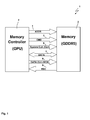
- the GDDR5-system 1 comprises a memory controller 2 (as a master) and a GDDR5-memory 3 (as a slave).
- the memory controller 2 and the memory 3 are connected by a variety of channels 4, 5, 6, 7, 8, 9. Some of the channels are unidirectional (channels 4, 5, 6, 8, 9) while presently one channel 7 (the data transfer line or data transfer channel) is bidirectional.
- an address channel 4 for transmitting address data from the memory controller 2 to the memory 3; a command channel 5 (CMD) for transmitting commands from the memory controller 2 to the memory 3, a system clock channel 6 (CLK) for transmitting a clocking signal from the memory controller 2 to the memory 3, a data clock channel 8 (WCK) for transmitting a second clocking signal from the memory controller 2 to the memory 3, an error detection signal 9 (EDC) for transmitting error signals and phasing information from the memory 3 to the memory controller 2 and a (bidirectional) data channel 7 (DATA) for transmitting data that is read out of the memory 3/written into the memory 3 by the memory controller 2.
- ADDR address channel 4
- CMD command channel 5
- CLK system clock channel 6
- WCK data clock channel 8
- EDC error detection signal 9
- DATA data channel 7
- the system clock 6 runs at a first frequency (for example 1 GHz).
- the data clock 8 runs at double frequency, i.e. presently at 2 GHz.
- the data on the data channel 7 is not only transmitted at a rising, but additionally at a falling flank of the data clock signal 8. Therefore data bits are transmitted on the data channel 7 at a rate of 4 GHz (i.e. at a transmission rate of 4 Gbps or 4 Giga bits per second).
- the signals that are transmitted between the memory controller chip 2 and the memory chips 3 are normally not perfectly adapted to each other (i.e. between the different chips). And even if a chip 2, 3 comes from the same manufacturer and is of the same quality level, part variances are inevitable, thus resulting in certain variations that can never be completely avoided.
- Every part involved in particular every chip 2, 3 from the memory system 1 has to be able to correctly handle signals with variations within a certain bandwidth.
- This minimum bandwidth that has to be tolerated is specified in the definition of the applicable standard (in the presently depicted case the JEDEC-standard).
- An example for this is the pulse width, the pulse voltage or the like.
- a training phase is also implemented in the JEDEC-standard (with respect to phasing adjustments) and is schematically illustrated in Fig. 2 .
- a system clocking signal 10 is transmitted at standard clocking rate on the system clock channel 6 (see Fig. 1 ).
- the system clocking signal 10 is essentially a repetitive rectangular signal at a certain frequency of presently 1 GHz.
- the data clock signal 11 on the data clock channel 8 is indicated in Fig. 2 .
- the data clock signal 11 presently runs at double frequency as compared to the system clock signal 10.
- command data 12 on the command channel 5 is also indicated.
- a command 12 bit is transmitted on every rising flank of the system's clocking signal 10, i.e. at 1 GHz rate.
- An address data 13 bit is transmitted on every rising and falling flank of the system clocking signal 10, i.e. at 2 GHz data transfer rate.
- a chunk of user data 14 is transmitted on every rising and falling flank of the data clock signal 11, i.e. presently at 4 GHz.
- the different phases of the different signals 10, 11, 12, 13, 14 are usually not very well aligned to each other. This is very problematic, because the memory system 1 is very vulnerable to phase shifts between the different signals.
- the vulnerability is particularly predominant for the user data 14 on data channel 7, since this signal is clocked by a different clocking signal, namely the data clock signal 11 as opposed to the system clocking signal 10.
- phase training sequence 15 is performed immediately after powering up 16 the memory system 1.
- a first step 17 and in a second step 18 the phase shift of the address data 13 on the address channel 4 with respect to the clocking signal 10 will be adjusted, (address training 17). Thence, a WCK2CK training loop 18 will be performed, in which the phasing of the data clock signal 11 and the system clock signal 10 will be adjusted. After this step 18, the phasing of the data signal 14 is adjusted (usually with respect to the data clock signal 11). This phasing adjustment is split up into two parts, namely the read training cycle 19 and the write training cycle 20. This is due to the fact since the time delays on the data channel 7 depend on the direction of the data transmitted. This is due to different electronic components used and variation of their individual characteristics (including part variances).
- an address training cycle 17 and a clock signal phasing training cycle 18 is initiated according to the amended training phase 22 (similar to the previously described phase training sequence 15). Also similar to the previously described phase training sequence 15, a read phasing training cycle 19 is initiated according to amended training phase 22.
- a receive equalizer training cycle 23 is interspersed.
- the user data 14 that is transmitted via the data channel 7 is compared with the identical user data that is transferred via a safe data channel (i.e. comparative data; more explanation will follow).
- the setting of the receive equalizer 33 will be performed in a way so that errors between the user data 14 transmitted on the data channel 7 and the comparative data will be below a certain threshold value, preferably minimised. Whether this condition has already been achieved will be checked in a consecutive interrogation step 24.
- the sequence will jump back to the read training cycle 19, again followed by another receive equalizer training cycle 23, according to the amended training phase 22. These steps will be repeated, until a satisfactory low error level has been reached. Then, the read training 19, 23 will be finished and the write training 20, 25 will be initiated, by first starting with the write phasing training cycle 20 (see also the respective step in phase training sequence 15 according to Fig. 2 ). Once the phasing of the user data 14 on the data channel 7 in write direction is established, a transmit equalizer training cycle 25 will be performed.
- step 25 If a sufficiently low error rate has not been established after this step 25 (which will be checked in a write data correctness interrogation step 26), the write training 20, 25 will be repeated using write phasing training cycle 20 and transmit equalizer training cycle 25. Once a sufficiently low error level has been established, both in a read and in a write direction, normal operation will start 27.
- the error rate of the memory system 1 will be continuously monitored 28. As long as the error rate is sufficiently low, normal operation 27 will continue. If, however, a certain threshold level will be exceeded (which can occur due to temperature differences, e.g. resulting from waste heat) a preferably complete amended training phase 22 will be re-initiated. This way, a good performance of the memory system can be sustained. It should be mentioned that the percentage of training phases with respect to overall running time is normally in the low single digit percentage region (if at all that high).
- Fig. 4 a schematic overview of a more elaborate memory system 29 with a memory controller 30 and a memory unit 31 is shown.
- some internal circuitries of the memory controller chip 30 and the memory chip 31 are additionally shown, while the different lines 4 to 9 that are interconnecting memory controller chip 30 and memory chip 31 are similar to the different channels 4 to 9, shown in Fig. 1 .
- the bidirectional data channel 7 is graphically split up into separate lines 7a, 7b (logical directional lines) in Fig. 4 .
- this is only done for illustrative purposes, thus representing the two different logical data transmission directions of the data channel line 7.
- the data channel 7 is a single, bidirectional data channel.
- a control unit 36 is provided for controlling both the transmit equalizer 32 and the receive equalizer 33.
- a variety of amplifiers 37 is present both in the memory controller chip 30 as well as in the memory chip 31.
- a memory unit 38 is indicated within memory chip 31.
- data can be temporarily stored, in particular user data transmitted via the data channel 7, as well as comparative data, transmitted (in the presently shown embodiment) on the address channel 4. These two chunks of data can then be compared with each other.
- the receive equalizer training cycle 23 (see Fig. 3 ) is performed in a way that test data is transmitted via the address channel 4.
- This can be implemented by first sending a certain command, for example via the command channel 5, indicating that for the time being test data (and no user data) is transmitted via the address channel 4.
- This test data is temporarily stored in memory unit 38.
- This temporal storage is necessary, since the transmission rate on the address channel 4 is lower as compared to the transmission rate of the data channel 7 (in particular 7b). Since the address channel 4 runs at a lower speed, the transmission can be considered to be reliable i.e. to be essentially error free.
- the test data transmitted on the address channel 4 is not only stored in memory unit 38, but also buffered in control unit 36.
- test data will be transmitted through the data channel 7 (in direction from memory chip 31 to memory controller chip 30, i.e. on "logical data channel 7b"). Now the looped back test data is compared with the test data buffered in control unit 36. Due to the characteristics of the different transmission channels 4, 7, it is assumed that any error that is present comes from the transmission via "logical data channel 7b". Hence, receive equalizer 33 is adapted by controller unit 36 in a way that the error rate will be set below a certain threshold value, preferably minimised (see read data correctness interrogation step 24 in Fig. 3 ).
- the second training cycle is initiated starting with a write phasing training cycle 20, and followed by a transmit equalizer 32 training cycle 25.
- data is generated and transmitted by the control unit 36 towards the memory chip 31 through "logical data channel 7a".
- the data, received by the memory chip 31 is directly sent back through a "logical read data channel 7b" (in reality a short buffering has to occur to avoid collisions). Since the "logical read data channel 7b" is considered to be error free, it is assumed that all errors occurring are induced by the "logical write data channel 7a". Based on this assumption, the transmit equalizer 32 is set up in a way by controller unit 36 to bring the error level below a certain threshold (which can be the same threshold as in the read case or a different threshold), preferably minimised.
- a certain threshold which can be the same threshold as in the read case or a different threshold
- a modified memory system 39 (which can be a different type of communication system as well) according to another embodiment is schematically shown. Similar to the embodiment 29 shown in Fig. 4 , a memory controller chip 40 is connected to a memory chip 41. However, the data channel not only consists of a single data line 7, but instead of a plurality of data lines 42, 43 (which are again split up "logically" in the two different directions a, b for illustrative purposes, although they are physically bidirectional data lines 42, 43). According to the embodiment shown in Fig. 5 , the training phases for the different data lines 42, 43 can be performed in series, one after another. The advantage of this embodiment is that a reduced amount of electronic devices is needed for this embodiment of a training phase. As a drawback, the training phase will take more time to complete. However, since training phases usually account for an only minor percentage of the total runtime, this is normally of no or only minor relevance.
- the memory system (communication system) according to Fig. 5 can be designed in a different way as well, in particular in a way that the training phases for the different data lines 42, 43 are performed in parallel to reduce the overall training time for all data lines 42, 43.
- the drawback of such a modified embodiment is the increased amount of electronic devices necessary. This increased amount of electronic devices can be reduced, if a transmitter/receiver pair of equalizers can be used for two or even more nearby data lines in granularity of 2 or more which have approximately the same (or at least similar) characteristics.
Landscapes
- Engineering & Computer Science (AREA)
- Computer Networks & Wireless Communication (AREA)
- Signal Processing (AREA)
- Power Engineering (AREA)
- Dc Digital Transmission (AREA)
Abstract
Description
- The invention relates to a method for improving the signal integrity of a data transfer line in a time synchronised data transfer system, wherein at least one equalizer unit is provided for said data transfer line. The invention also relates to an equalizer unit for a time synchronised data transfer system. Furthermore the invention relates to an electronic device comprising a synchronised data transfer system.
- In nowadays digital electronics, data has to be transferred between various units frequently. The transfer of data not only has to be performed between different units (for example between different computers or workstations in a computer network or in a computer cluster), but also between subunits inside a single unit. As an example for the latter, computer busses that are used to transfer data between the CPU (central processing unit), the electronic memory (usually RAM = random access memory), a graphics card, a hard disk drive etc. can be mentioned. However, the necessity for a data transfer does not stop at this level, but even goes beyond.
- As an example, even within a computer memory board or on the graphics card itself, a huge amount of data transfer has to be performed. As an example, nowadays computer memory systems are typically divided into a memory controller serving a plurality of memory chips using a 32 bit data bus (or an even wider data bus). Hence, a data transfer at an appropriate data transfer rate has to be provided for the communication between the respective memory controller chip and the memory chips themselves. Another example is the communication between GPUs (graphic processing units) and the graphic data memory chips (typically all arranged on a computer graphics card or a computer video card).
- Depending on the devices to be coupled together (i.e. depending on the actual application) and particularly based on economic considerations, an appropriate maximum data transfer rate has to be chosen. As a rule of thumb, a good compromise between a data rate that is as high as possible (for performance reasons) and a resulting data transfer device that is as cheap as possible (and hence typically slow with respect to maximum data transmission rate) has to be chosen. A good compromise will be typically based on the application. While a data transfer between two computers with a data transfer rate of 10 Mbit/sec may be more than enough for standard applications, such a data transfer rate will be way too low for a data transfer between a CPU and an electronic memory unit and/or within an electronic memory module.
- In general, data transfer protocols can be divided into synchronous data transfer protocols and asynchronous data transfer protocols.
- Roughly speaking, asynchronous data transfer protocols are typically cheaper to implement and have the advantage that different units with a strongly varying design and performance can be connected to each other. The big drawback of asynchronous computer protocols is their comparatively slow speed which is in part based on the amount of a data transfer that is required for the handshake protocol. The big advantage is the typically comparatively low hardware requirements, and that typically comparatively few cables have to be used for interconnecting the respective units with each other. A typical example for asynchronous data transfer protocols are the Ethernet, LAN (local area networks) and/or DSL connections (DSL = digital subscriber line). It has to be noted that even here usually a synchronisation is done. However, if such a synchronisation is performed, this is usually done on a frame level, and not on a clocking signal level.
- On the other side, there are the synchronous data transfer protocols. Typically, when using synchronous data transfer protocols the resulting data transfer rates are significantly higher as compared to asynchronous data transfer methods. This is of course a big advantage. As a drawback, the hardware requirements are higher. In particular, quite often several clocking signals have to be provided and/or usually a comparatively high number of connecting wires are used and/or very high frequencies have to be used for data transfer. Furthermore, the units that are connected with each other by a synchronous data connection usually have to have a somewhat similar performance. A typical example for the use of synchronous data transfer methods are computer busses within a computer and/or the data transfer that is performed between a memory controller and the memory storage chips and/or between a GPU and graphic memory chips.
- To increase the data transfer rate of synchronous data transfer protocols even further without unduly increasing the power consumption and/or the cost for the electronic devices needed, different clocking speeds have been used for the interconnecting lines between two electronic devices to be connected to each other. For illustrative purposes, let's have a look at a data transfer that is effectuated between a memory controller (serving as a master) and the memory storage chips (working as slaves) in a GDDR5-memory system. Here, as an example, a main clocking signal of 1 GHz (basic frequency) is used. This frequency is used for transmitting commands and addresses over a respective data transfer line. However, the "real" data transfer (i.e. the data that is read out of and/or that is written into the indicated address) is transferred based on a second clocking signal (the write clocking signal or forward clocking signal, typically abbreviated as WCK) where the second clocking signal typically runs at a frequency, twice as high as the main clocking signal (typically abbreviated as CK or CLK). Moreover, a data bit is usually not only transmitted on a rising flank of the WCK signal, but also on a falling flank of the WCK signal. This way, a data transfer rate of 4 Gbit/sec can be realised (typically transferred on a dedicated data transfer line (usually abbreviated as DATA or DQ).
- Transmitting data at such high frequencies raises various problems. In particular, signals that are transmitted on the individual lines fall clearly in the radio frequency range. The individual lines act as small transmitting and receiving antennas, so that the respective signal is in part transferred to other lines as well. This effect is generally known as the cross talk effect (X talk). Furthermore, the individual lines show a certain inductance and electric capacitance, which leads to a certain signal degradation on the transmitting line. This is known as the intersymbol interference (ISI). To be able to connect electronic components of various manufacturers with each other, certain quality standards that have to be obeyed by the respective manufacturer have been defined. To continue with the example of a GDDR5-memory system, such standards have been defined in the so-called JEDEC-standard. However, obeying such standards requires a certain quality level of the respective electronic components. This results in a certain minimum production cost. However, since the price of memory chips has a significant impact on the overall price of electronic devices, a further reduction of prices for electronic memory is desired. Furthermore, it would be desirable to increase the data transfer rates, preferably without increasing the price for the respective components (at least not linearly).
- A method for improving the performance of an interconnection between integrated circuit devices has been suggested in United States patent application
US 2011/0310949 A1 . Here, it is suggested to provide a signalling system with a pre-emphasising transmitter and an equalizing receiver that are coupled to one another via a high-speed signal path. The receiver measures the quality of data conveyed from the transmitter. A controller uses this information to adaptively establish appropriate transmit pre-emphasis and receive equalization settings, e.g. to select the lowest power setting for which the signalling system provides some minimum communication bandwidth without exceeding a desired bit-error rate. However, this approach requires comparatively elaborate electronics on both sides of the signal path. This will increase the overall cost of the resulting electronic device significantly. This is particularly the case, because a typically significant number of slave-chips has to be equipped with complex electronics. Additional cost and power consumption comes from the necessary controller unit used for controlling the signalling systems components. Another problem is that the control of the pre-emphasising transmitter and the equalizing receiver is based on the bit-error rate of the signals transmitted via the high-speed signal path. Therefore, depending on the error detection system used, it can take a considerable time until an acceptable setting can be reached (if at all). Another major problem is that the system, described inUS 2011/0310949 A1 is not compatible with present memory systems (in particular with DDR memory systems, in particular with GDDR5 memory systems). This poses a major obstacle for the use of this system. - Therefore, there is a significant need for an improved method for improving the signal integrity of a data transfer line in a time synchronised data transfer system as well as for improved equalizer units and/or digital devices comprising a time synchronised data transfer system.
- It is therefore the object of the invention to provide a method for improving the signal integrity of a data transfer line in a time synchronised data transfer system that is improved over presently known methods for improving the signal integrity of such a data transfer line. It is another object of the invention to propose an equalizer unit that is improved over presently known equalizer units. It is yet another object of the invention to provide an electronic device that comprises a synchronised data transfer system that is improved over presently known electronic devices.
- The invention solves these objects.
- It is suggested to perform a method for improving the signal integrity of a data transfer line in a time synchronised data transfer system, wherein at least one equalizer unit is provided for said data transfer line and wherein a training phase, comprising at least one training cycle for adjustment of the settings of said at least one equalizer unit, is used in a way that said adjustment of the settings of said at least one equalizer unit is at least in part based on transmitting test data via said data transfer line to be trained and that said test data is compared with comparative data that is transferred via a safe transmission channel. Training phases are frequently used in time synchronised data transfer system. During such a training phase, certain settings of the transmitter and/or the receiver part of the data transfer system are optimised to reduce the error rate, to reduce the power consumption and/or to increase the achievable data transfer rate. So far, however, training phases usually have been restricted to correct for a phase difference between the various components. Other adjustments have hardly been proposed in the state of the art (if at all). One of the few examples that equalizers are used for data transmissions and that the settings of the equalizers are adjusted is described in
US 2011/0310949 A1 . In this publication, the use and a possible setup of an equalizer for a data transfer line is described. However, for the present invention a wide variety of different equalizers can be employed. Just to name another example, inUS 5,228,058 A another possible equalizer is described. The equalizer unit can be provided at any side of the data transfer line. In other words, both transmit equalizers and/or receive equalizers can be used in the present context. The data transfer line is preferably a data transfer line that is provided for data transfer. In the example of a GDDR5-chip, this would be preferably the data transfer line (usually DQ-line) on which the "normal" data is transmitted. Such a data transfer line is usually operating at a comparatively high data transfer rate, in particular at a higher clocking speed as compared to (at least some of) the other lines. As an example, the DQ-line is usually operated at double or quadruple speed as opposed to the other lines. Of course, one has to admit that at least some of the other lines transmit data as well, for example a memory address line (usually referred to as ADDR) transfers some data as well, namely the address information, even with presently commercially available chips. However, here the data transfer is usually performed at a lower frequency as compared to the "real data channel" (usually at standard clocking speed). One aspect of the invention lies in the idea to use "real" data (i.e. test data) for adjusting the settings of the at least one equalizer unit. This data is transferred on the data transfer line, preferably at "usual" data transfer conditions. In particular, full data transfer rate is employed for transmitting the test data. Therefore, a "realistic" picture of the current transmission characteristics is obtained and hence a better adjustment can be performed. Another aspect of the invention lies in the idea to not rely on any error detection algorithm or the like. This can be problematic, since such algorithms can result in wrong or ambiguous results (in particular if the overhead is minimised) or can alternatively result in a significant overhead (in particular if the probabilities of errors have to be minimised). According to the present suggestion, the test data is compared with comparative data that is transferred via a safe transmission channel. Usually, the comparative data is (at least in part) the same as the test data. This way usually improved results can be achieved. The data (test data and/or comparative data) preferably resembles "usually transmitted data". For example, typically transmitted bit patterns can be used for this. This will usually result in an improvement over standard repetitive patterns (like a continuous alternating stream of 0's and 1's and/or a continuous series of (sets of) identical bites. To obtain "realistic data", an advantageous dataset can be stored or a pseudorandom pattern can be transmitted. The safe transmission channel can be generated in a plethora of ways. As an example, the data transmission can be performed during manufacture of the respective devices so that "standard datasets" (in particular according to a certain standard) are stored and compared during a booting sequence. However, it is also possible to perform a "real data transmission" between the components on both sides of the data transfer line. The safe transmission can be employed, for example, by temporarily using a "safer error correction algorithm", a different data line, a different clocking speed and/or different data transmission protocols that are particularly safe. Safe in the context of this description usually means that very few errors occur during the transmission. In particular, few errors, as compared to the error rate of test data on the test data line, should occur during transmission. However, it should be mentioned that even some errors during transmission on the safe transmission channel usually do not pose a particular problem. Usually, an error "once in a while" will be considered to be a "not yet optimum setting of the equalizer", and hence the training phase will be somewhat prolonged. - In general, any kind of equalizer unit can be used, employing essentially any thinkable modification of the transmitted data. Preferably, however, the at least one equalizer unit alters the voltage level and/or the signal shape and/or the duty cycle of the data signal on said data transfer line. These modifications will usually have the greatest impact when trying to reduce the error rate on the data transfer line. Therefore, if these modifications are performed, usually the most efficient equalizer unit can be realised (resulting in a good compromise between best signal alteration and still simple setup of the equalizer unit).
- Preferably, the method is employed in a way that said test data and/or said comparative data is at least at times stored, preferably temporarily stored. Storing can be done during the production of the respective components for the components of one or both sides (in the case of memory systems for slave components and/or for master components). For this, a certain standard data pattern can be used (which should be defined according to a certain standard). Additionally or alternatively a temporal storage is possible as well. This way, transmission of test data and/or comparative data at different transmission speeds and/or via different transmission lines (usually showing different delays) can be performed and still such data can be compared. Furthermore, when data is temporarily stored, a transmission of test data and comparative data in series, even on the same line, is possible (where the transmission is probably performed at a different data transmission rate). Also, a "loop back type test" can be performed so that data can be sent out, returned and compared with the originally sent data.
- Preferably, the data transfer line is a bidirectional data transfer line. This way, a comparatively simple setup can be used (in particular additional pins, lines and/or space can be saved). Normally, no significant performance degradation will result from this, because usually data is only transmitted in one direction at a time anyhow (as it is usually the case with computer memory and/or computer graphics memory). It should be mentioned that the transmission characteristics of a bidirectional data transfer line can be different for the two directions. Therefore, either a "compromise" setting of the equalizer can be chosen, so that "both directions are served well on the average" (where statistical considerations with respect to the ratio between sending and receiving can be taken into account as well), or different settings are used depending on the direction of the data transfer. However, the presently suggested invention can be used with unidirectional data transfer lines as well.
- It is further suggested to use at least two equalizer units, wherein said two equalizer units are preferably arranged on a single side of said data transfer line. Although it is in principle possible to use a single equalizer unit and to presumably readjust it depending on the direction of the data transmission, usually a better result can be obtained if separate equalizers are used. In particular it is possible to optimise the respective equalizer (for example a transmit equalizer and a receive equalizer) for its respective task, even on the hardware side. This can result in an even higher performance. If said two equalizer units are arranged on a single side of said data transfer line, only one component has to be modified. This suggestion can prove to be very advantageous, because usually in time synchronised data transfer systems, a single master unit serves a plurality of slave units. If hence the modification of providing equalizers is performed on the master side, only a comparatively small percentage of the overall components have to be provided with additional components. This way, the overall cost usually does not increase significantly. Surprisingly, it is even possible to reduce the overall cost. This is, because the minimum standard required for the data transmission can be relaxed (because a degraded signal quality can usually be compensated by appropriately adjusted equalizers). This way, the hardware requirements of some of the components (in particular of slave components) can be reduced. This way, those devices can be produced cheaper. On the average, the net effect can be in a way that the overall arrangement is even cheaper as compared to present arrangements. In this context it should be mentioned that a higher signal quality "per se" does not pose any problem. This way, it is possible to use (just to name an example) an "improved" memory controller (that is designed according to the present suggestion), both in connection with "standard" memory chips (i.e. obeying present JEDEC-standards), but also with "inferior" memory chips (i.e. memory chips with relaxed system specifications). This possibility can increase the acceptance of the presently suggested method and system significantly.
- A preferred embodiment of the method can be realised if said training phase comprises at least two training cycles, preferably at least one training cycle for a data transfer in a first direction and at least one training cycle for a data transfer in a second direction. The training cycles in this context generally relate to training cycles for adjusting the settings of equalizer units. As already mentioned, the transmission characteristics of data transmission lines usually depend on the direction of the data transfer, even when a single, bidirectional data transmission line is used. If both directions are considered during training, usually a better overall training can be achieved, thus resulting in an increased data transfer performance.
- A possible embodiment of the method can be realised if said data transfer line is used at least at times for transmitting comparative data if the integrity of the data transmission is secured, at least in the respective direction. This way, it is possible to train a bidirectional data transfer line in a first step in a first direction by using a memory address line (for example) for transmitting the comparative data. After the equalizer settings for this direction have been determined and employed, one can rely on the integrity of the data transmitted on the data transmission line in this direction. Now, one can use the data transfer line as a safe data transfer line in this direction. In a second step, the settings of (usually) another equalizer for improving the data transfer characteristics in the opposite direction can be determined. For completeness it should be mentioned that the transmitted data can preferably be (temporarily) stored on both sides of the data transmission line. This way, the direction of the data transmission of the test data and the direction of the data transmission of the comparative data can point in different directions. This way, a "loopback" can be realised. However, it is of course possible as well, that both test data and comparative data are sent in the same direction.
- It is possible to realise the safe transfer channel in a wide variety of ways. However, first experiments have shown that it is preferred if the safe transfer channel is realised at least at times by using an alternative data line and/or by using safe data transfer characteristics. The alternative data line can be a data line that is provided for other purposes (for example a memory address line or an error correction line or the like), or can be a line that is (essentially) reserved for transmitting comparative data. Additionally or alternatively, safe data transfer characteristics can be employed for transmitting the comparative data. As an example, a lower data transfer speed, a better signal quality (using more energy and/or producing more waste heat) or the like can be used.
- It is particularly preferred if the safe transfer line is a line that is used at times for purposes of said training phase and used at times for other purposes. This way, the number of hardware lines can be reduced. In particular, a line can be used which has to be "present anyhow", for example a memory address transmission line, an error detection line or the like.
- Preferably, the method is employed in a way that said training phase comprises at least one additional training cycle, in particular a phase adjusting training cycle. By the expression "additional training cycle" in particular a training cycle that is different from a training cycle for adjusting the setting of an equalizer is meant. Although a wide variety of training cycles can be considered, first experiments have shown that in particular a phase adjusting step results in a particular predominant improvement of the data transfer characteristics. In particular, it is possible to use a phase adjusting training cycle as described in European patent application with filing number
EP 12174388.4 - Another preferred embodiment of the method can be realised if said training phase and/or at least one training cycle can be repeated. It is possible that the training cycle is "instantaneously" repeated (in particular after finishing a previous training cycle and/or even during the same training phase and/or immediately following a previous training phase) if a checking step reveals that no suitable data transfer performance has been established. However, the repetition can be performed "somewhat later" as well, for example if a continuous monitoring of the data transmission reveals that a degradation of the data transmission has taken place. In such a case, a "retraining" can be performed once in a while. This way, an advantageous data transfer can be sustained, even for prolonged periods of time.
- In particular, the method can be used for a data transfer line that is at least at times operated with an increased data transfer rate. As an example, the data transfer rate can be performed at double, quadruple or even higher speeds, as compared to the clocking speed of the "remaining" components. In particular, such a "high speed" data transfer line is particularly prone to transmission errors; hence, an improvement of the signal integrity on such a line is particularly rewarding.
- In particular, the presently suggested method can be employed for synchronising a memory controller and a memory unit, in particular of a DDR-memory type (DDR = double data rate). For such fields of application, the intrinsic features and advantages of the presently proposed methods are usually particularly predominant.
- Furthermore, an equalizer unit is suggested, wherein the equalizer unit is designed and arranged in a way to perform at least at times a method according to the previous description. In such a case, the equalizer unit can show the same features and advantages, as previously described, at least in analogy. Furthermore, the equalizer unit can be modified in the sense of the previous description, at least in analogy.
- Even more, an electronic device, in particular a memory controller unit and/or a memory unit is suggested, that comprises at least one equalizer unit according to the previous description and/or that is designed and arranged in a way to perform at least at times a method according to the previous description. In particular, at least a part of said electronic device can comprise one or more integrated circuits and/or can be a part of at least one integrated circuit and/or can be (at least in part) a digital device. This way, the device can show the same features and advantages, as previously described, at least in analogy. Furthermore, the electronic device can be modified in the previous sense, at least in analogy, as well.
- The present invention and its advantages will become more apparent, when looking at the following description of possible embodiments of the invention, which will be described with reference to the accompanying figures, which are showing:
- Fig. 1:
- the schematic circuitry of a memory system with a memory controller and a memory chip according to a first embodiment of a communication system;
- Fig. 2:
- an illustration of phase shift relations and an embodiment of a training cycle for adjusting them;
- Fig. 3:
- a possible embodiment of a training phase of a memory system after power up in a schematic flowchart;
- Fig. 4:
- a first embodiment of a memory system with an adaptive equalizer arrangement;
- Fig. 5:
- a second embodiment of a memory system with an equalizer arrangement.
- In
Fig. 1 a schematic drawing of a typical example of a memory system - presently a GDDR5-system 1 - according to JEDEC-standard is shown (GDDR = graphical double data rate memory). The GDDR5-system 1 comprises a memory controller 2 (as a master) and a GDDR5-memory 3 (as a slave). Thememory controller 2 and thememory 3 are connected by a variety ofchannels channels memory controller 2 to thememory 3; a command channel 5 (CMD) for transmitting commands from thememory controller 2 to thememory 3, a system clock channel 6 (CLK) for transmitting a clocking signal from thememory controller 2 to thememory 3, a data clock channel 8 (WCK) for transmitting a second clocking signal from thememory controller 2 to thememory 3, an error detection signal 9 (EDC) for transmitting error signals and phasing information from thememory 3 to thememory controller 2 and a (bidirectional) data channel 7 (DATA) for transmitting data that is read out of thememory 3/written into thememory 3 by thememory controller 2. - As implemented in the GDDR5-standard according to JEDEC specifications, the
system clock 6 runs at a first frequency (for example 1 GHz). Thedata clock 8 runs at double frequency, i.e. presently at 2 GHz. The data on thedata channel 7 is not only transmitted at a rising, but additionally at a falling flank of thedata clock signal 8. Therefore data bits are transmitted on thedata channel 7 at a rate of 4 GHz (i.e. at a transmission rate of 4 Gbps or 4 Giga bits per second). - Since the
memory controller 2 and thememory 3 are usually from different manufacturers and sometimes of a different quality class, the signals that are transmitted between thememory controller chip 2 and thememory chips 3 are normally not perfectly adapted to each other (i.e. between the different chips). And even if achip - To account for these variations, a first approach is that every part involved (in particular every
chip - Another approach to handle these variations is to perform a training phase. Such a training phase is also implemented in the JEDEC-standard (with respect to phasing adjustments) and is schematically illustrated in
Fig. 2 . On the right side ofFig. 2 , different clocking signals anddifferent signals channels system clocking signal 10 is transmitted at standard clocking rate on the system clock channel 6 (seeFig. 1 ). Thesystem clocking signal 10 is essentially a repetitive rectangular signal at a certain frequency of presently 1 GHz. Furthermore, thedata clock signal 11 on thedata clock channel 8 is indicated inFig. 2 . Thedata clock signal 11 presently runs at double frequency as compared to thesystem clock signal 10. Furthermore, thecommand data 12 on thecommand channel 5, theaddress data 13 on theaddress channel 4 and theuser data 14 on thedata channel 7 are also indicated. As can be seen, in the presently shown embodiment of amemory system 1, acommand 12 bit is transmitted on every rising flank of the system'sclocking signal 10, i.e. at 1 GHz rate. Anaddress data 13 bit is transmitted on every rising and falling flank of thesystem clocking signal 10, i.e. at 2 GHz data transfer rate. Lastly, a chunk ofuser data 14 is transmitted on every rising and falling flank of thedata clock signal 11, i.e. presently at 4 GHz. - When powering up the
memory system 1, the different phases of thedifferent signals memory system 1 is very vulnerable to phase shifts between the different signals. The vulnerability is particularly predominant for theuser data 14 ondata channel 7, since this signal is clocked by a different clocking signal, namely thedata clock signal 11 as opposed to thesystem clocking signal 10. - Therefore, according to current JEDEC-specification, a
phase training sequence 15 is performed immediately after powering up 16 thememory system 1. - In a
first step 17 and in asecond step 18 the phase shift of theaddress data 13 on theaddress channel 4 with respect to theclocking signal 10 will be adjusted, (address training 17). Thence, aWCK2CK training loop 18 will be performed, in which the phasing of thedata clock signal 11 and thesystem clock signal 10 will be adjusted. After thisstep 18, the phasing of the data signal 14 is adjusted (usually with respect to the data clock signal 11). This phasing adjustment is split up into two parts, namely the readtraining cycle 19 and thewrite training cycle 20. This is due to the fact since the time delays on thedata channel 7 depend on the direction of the data transmitted. This is due to different electronic components used and variation of their individual characteristics (including part variances). - According to present JEDEC-standards, after the read
training cycle 19 and thewrite training cycle 20 the powering up training phase is completed and normal operation starts 21. - However, significantly improved results can be obtained, if an amended
training phase 22 is used at start-up. A possible embodiment of such an amendedtraining phase 22 is shown as a flowchart inFig. 3 . - After initially powering up 16 the memory system 1 (or another electronic device), an
address training cycle 17 and a clock signal phasingtraining cycle 18 is initiated according to the amended training phase 22 (similar to the previously described phase training sequence 15). Also similar to the previously describedphase training sequence 15, a read phasingtraining cycle 19 is initiated according to amendedtraining phase 22. - After the phasing of the read
signal 14 on thedata channel 7 is completed, however, a receiveequalizer training cycle 23 is interspersed. Here, theuser data 14 that is transmitted via thedata channel 7 is compared with the identical user data that is transferred via a safe data channel (i.e. comparative data; more explanation will follow). The setting of the receiveequalizer 33 will be performed in a way so that errors between theuser data 14 transmitted on thedata channel 7 and the comparative data will be below a certain threshold value, preferably minimised. Whether this condition has already been achieved will be checked in aconsecutive interrogation step 24. If the read data (user data 14 transmitted on data channel 7) is not yet correct, the sequence will jump back to the readtraining cycle 19, again followed by another receiveequalizer training cycle 23, according to the amendedtraining phase 22. These steps will be repeated, until a satisfactory low error level has been reached. Then, the readtraining write training phase training sequence 15 according toFig. 2 ). Once the phasing of theuser data 14 on thedata channel 7 in write direction is established, a transmitequalizer training cycle 25 will be performed. If a sufficiently low error rate has not been established after this step 25 (which will be checked in a write data correctness interrogation step 26), thewrite training training cycle 20 and transmitequalizer training cycle 25. Once a sufficiently low error level has been established, both in a read and in a write direction, normal operation will start 27. - Preferably, the error rate of the
memory system 1 will be continuously monitored 28. As long as the error rate is sufficiently low,normal operation 27 will continue. If, however, a certain threshold level will be exceeded (which can occur due to temperature differences, e.g. resulting from waste heat) a preferably complete amendedtraining phase 22 will be re-initiated. This way, a good performance of the memory system can be sustained. It should be mentioned that the percentage of training phases with respect to overall running time is normally in the low single digit percentage region (if at all that high). - In
Fig. 4 , a schematic overview of a moreelaborate memory system 29 with amemory controller 30 and amemory unit 31 is shown. In particular, some internal circuitries of thememory controller chip 30 and thememory chip 31 are additionally shown, while thedifferent lines 4 to 9 that are interconnectingmemory controller chip 30 andmemory chip 31 are similar to thedifferent channels 4 to 9, shown inFig. 1 . However, for illustrative purposes, thebidirectional data channel 7 is graphically split up intoseparate lines Fig. 4 . However, this is only done for illustrative purposes, thus representing the two different logical data transmission directions of thedata channel line 7. Physically, thedata channel 7 is a single, bidirectional data channel. - As indicated in the flowchart of the amended
training phase 22, shown inFig. 3 , a transmitequalizer 32 and a receiveequalizer 33 that is presently comprised of a non-linear equalizer 34 (usually known as a DFE = decision feedback equalizer) and a linear equalizer 35 (commonly known as LEQ = linear equalizer) is provided. Furthermore, acontrol unit 36 is provided for controlling both the transmitequalizer 32 and the receiveequalizer 33. Furthermore, a variety ofamplifiers 37 is present both in thememory controller chip 30 as well as in thememory chip 31. Furthermore, amemory unit 38 is indicated withinmemory chip 31. Thememory unit 38 is of a so-called FIFO-type (FIFO = first in first out). In thememory unit 38 data can be temporarily stored, in particular user data transmitted via thedata channel 7, as well as comparative data, transmitted (in the presently shown embodiment) on theaddress channel 4. These two chunks of data can then be compared with each other. - The receive equalizer training cycle 23 (see
Fig. 3 ) is performed in a way that test data is transmitted via theaddress channel 4. This can be implemented by first sending a certain command, for example via thecommand channel 5, indicating that for the time being test data (and no user data) is transmitted via theaddress channel 4. This test data is temporarily stored inmemory unit 38. This temporal storage is necessary, since the transmission rate on theaddress channel 4 is lower as compared to the transmission rate of the data channel 7 (in particular 7b). Since theaddress channel 4 runs at a lower speed, the transmission can be considered to be reliable i.e. to be essentially error free. Of course, the test data transmitted on theaddress channel 4 is not only stored inmemory unit 38, but also buffered incontrol unit 36. Once thememory unit 38 has stored a certain amount of data, the test data will be transmitted through the data channel 7 (in direction frommemory chip 31 tomemory controller chip 30, i.e. on "logical data channel 7b"). Now the looped back test data is compared with the test data buffered incontrol unit 36. Due to the characteristics of thedifferent transmission channels logical data channel 7b". Hence, receiveequalizer 33 is adapted bycontroller unit 36 in a way that the error rate will be set below a certain threshold value, preferably minimised (see read datacorrectness interrogation step 24 inFig. 3 ). - Now after training of the "logical
read data channel 7b", this data channel is considered to be "safe" in this direction (i.e. essentially error free). Now, the second training cycle is initiated starting with a write phasingtraining cycle 20, and followed by a transmitequalizer 32training cycle 25. In the latter, data is generated and transmitted by thecontrol unit 36 towards thememory chip 31 through "logical data channel 7a". The data, received by thememory chip 31 is directly sent back through a "logicalread data channel 7b" (in reality a short buffering has to occur to avoid collisions). Since the "logicalread data channel 7b" is considered to be error free, it is assumed that all errors occurring are induced by the "logicalwrite data channel 7a". Based on this assumption, the transmitequalizer 32 is set up in a way bycontroller unit 36 to bring the error level below a certain threshold (which can be the same threshold as in the read case or a different threshold), preferably minimised. - Once both read and write training cycles are completed, the
memory system 29 is ready for operation. - Although the training phase was described with respect to a
memory system 29, using certain types ofequalizers - In
Fig. 5 , a modified memory system 39 (which can be a different type of communication system as well) according to another embodiment is schematically shown. Similar to theembodiment 29 shown inFig. 4 , amemory controller chip 40 is connected to amemory chip 41. However, the data channel not only consists of asingle data line 7, but instead of a plurality of data lines 42, 43 (which are again split up "logically" in the two different directions a, b for illustrative purposes, although they are physically bidirectional data lines 42, 43). According to the embodiment shown inFig. 5 , the training phases for the different data lines 42, 43 can be performed in series, one after another. The advantage of this embodiment is that a reduced amount of electronic devices is needed for this embodiment of a training phase. As a drawback, the training phase will take more time to complete. However, since training phases usually account for an only minor percentage of the total runtime, this is normally of no or only minor relevance. - However, the memory system (communication system) according to
Fig. 5 can be designed in a different way as well, in particular in a way that the training phases for the different data lines 42, 43 are performed in parallel to reduce the overall training time for all data lines 42, 43. The drawback of such a modified embodiment is the increased amount of electronic devices necessary. This increased amount of electronic devices can be reduced, if a transmitter/receiver pair of equalizers can be used for two or even more nearby data lines in granularity of 2 or more which have approximately the same (or at least similar) characteristics. -
- 1. GDDR5-system
- 2. memory controller
- 3. GDDR5-memory
- 4. address channel
- 5. command channel
- 6. system clock channel
- 7. data channel
- 8. data clock channel
- 9. error detection signal channel
- 10. system clock signal
- 11. data clock signal
- 12. command data
- 13. address data
- 14. user data
- 15. phase training sequence
- 16. power up
- 17. address phase training cycle
- 18. clock signal phase training cycle
- 19. read phasing training cycle
- 20. write phasing training cycle
- 21. start of normal operation
- 22. amended training phase
- 23. receive equalizer training cycle
- 24. read data correctness interrogation
- 25. transmit equalizer training cycle
- 26. write data correctness interrogation
- 27. start of normal operation
- 28. monitoring of error rate
- 29. memory system
- 30. memory controller
- 31. memory chip
- 32. transmit equalizer
- 33. receive equalizer
- 34. non-linear equalizer
- 35. linear equalizer
- 36. control unit
- 37. amplifier
- 38. memory unit
- 39. modified memory system
- 40. memory controller
- 41. memory chip
- 42. data channel
- 43. data channel
Claims (15)
- Method (22) for improving the signal integrity of a data transfer line (7, 42, 43) in a time synchronised data transfer system (1, 29, 39), wherein at least one equalizer unit (32, 33, 34, 35) is provided for said data transfer line (7, 42, 43), wherein a training phase (15, 22) is used, comprising at least one training cycle (23, 25) for adjustment of the settings of said at least one equalizer unit (32, 33, 34, 35), characterised in that said adjustment of the settings of said at least one equalizer unit (32, 33, 34, 35) is at least in part based on transmitting test data via said data transfer line (7, 42, 43) to be trained and comparing said test data with comparative data that is transferred via a safe transmission channel (4, 5).
- Method (22) according to claim 1, characterised in that said at least one equalizer unit (32, 33, 34, 35) alters the voltage level and/or the signal shape and/or the duty cycle of the data signal on said data transfer line (7, 42, 43).
- Method (22) according to claim 1 or 2, characterised in that said test data and/or said comparative data is at least at times stored (38), preferably temporarily stored.
- Method (22) according to any of the preceding claims, characterised in that said data transfer line (7, 42, 43) is a bidirectional data transfer line (7, 42, 43).
- Method (22) according to any of the preceding claims, in particular according to claim 4, characterised in that at least two equalizer units (32, 33, 34, 35) are used, wherein said two equalizer units (32, 33, 34, 35) are preferably arranged on a single side (30, 40) of said data transfer line (7, 42, 43).
- Method (22) according to any of the preceding claims, in particular according to claim 4 or 5, characterised in that said training phase (15, 22) comprises at least two training cycles (23, 25), preferably at least one training cycle (23) for a data transfer in a first direction (7b, 42b, 43b) and at least one training cycle (25) for a data transfer in a second direction (7a, 42a, 43a).
- Method (22) according to any of the preceding claims, in particular according to claim 6, characterised in that said data transfer line (7, 42, 43) is used, at least at times, for transmitting comparative data if the integrity of the data transmission is secured, at least in the respective direction (7a, 42a, 43a).
- Method (22) according to any of the preceding claims, characterised in that a safe transfer channel (4, 5, 7a, 42a, 43a) is realised at least at times by using an alternative data line (4, 5) and/or by using safe data transfer characteristics.
- Method (22) according to any of the preceding claims, characterised in that the safe transfer line (4, 5) is a line that is used at times for purposes of said training phase and used at times for other purposes (12, 13).
- Method (22) according to any of the preceding claims, characterised in that said training phase (15, 22) comprises at least one additional training cycle (17, 18, 19, 20), in particular a phase adjusting training cycle (17, 18, 19, 20).
- Method (22) according to any of the preceding claims, characterised in that said training phase (15, 22) and/or at least one training cycle (17, 18, 19, 20, 23, 25) can be repeated (24, 26, 28).
- Method (22) according to any of the preceding claims, characterised in that the data transfer line (7, 42, 43) is at least at times a data transfer line with an increased data transfer rate (7, 42, 43).
- Method (22) according to any of the preceding claims, characterised in that it is used for synchronising a memory controller (30, 40) and a memory unit (31, 41), in particular of a DDR-memory type.
- Equalizer unit (32, 33, 34, 35), characterised in that the equalizer unit is designed and arranged in a way to perform at least at times a method (22) according to any of the preceding claims 1 to 13.
- Electronic device (1, 29, 39), in particular memory controller unit (30, 40) and/or memory unit (31, 41), characterised by at least one equalizer unit (32, 33, 34, 35) according to claim 14 and/or characterised in that it is designed and arranged in a way to perform at least at times a method (22) according to any of claims 1 to 13.
Priority Applications (1)
| Application Number | Priority Date | Filing Date | Title |
|---|---|---|---|
| EP12183643.1A EP2706712B1 (en) | 2012-09-10 | 2012-09-10 | Method and system for improving data transfer integrity |
Applications Claiming Priority (1)
| Application Number | Priority Date | Filing Date | Title |
|---|---|---|---|
| EP12183643.1A EP2706712B1 (en) | 2012-09-10 | 2012-09-10 | Method and system for improving data transfer integrity |
Publications (2)
| Publication Number | Publication Date |
|---|---|
| EP2706712A1 true EP2706712A1 (en) | 2014-03-12 |
| EP2706712B1 EP2706712B1 (en) | 2017-06-07 |
Family
ID=46888920
Family Applications (1)
| Application Number | Title | Priority Date | Filing Date |
|---|---|---|---|
| EP12183643.1A Not-in-force EP2706712B1 (en) | 2012-09-10 | 2012-09-10 | Method and system for improving data transfer integrity |
Country Status (1)
| Country | Link |
|---|---|
| EP (1) | EP2706712B1 (en) |
Cited By (1)
| Publication number | Priority date | Publication date | Assignee | Title |
|---|---|---|---|---|
| CN113742273A (en) * | 2020-05-30 | 2021-12-03 | 华为技术有限公司 | Balance training method, device and system |
Families Citing this family (2)
| Publication number | Priority date | Publication date | Assignee | Title |
|---|---|---|---|---|
| US11626180B2 (en) | 2021-05-11 | 2023-04-11 | Micron Technology, Inc. | Memory degradation detection and management |
| US11651834B2 (en) | 2021-05-11 | 2023-05-16 | Micron Technology, Inc. | Memory duty-cycle skew management |
Citations (4)
| Publication number | Priority date | Publication date | Assignee | Title |
|---|---|---|---|---|
| US5228058A (en) | 1990-07-17 | 1993-07-13 | Nec Corporation | Adaptive equalizer |
| EP1217438A2 (en) | 1988-04-18 | 2002-06-26 | 3D Systems, Inc. | Stereolithography using different types of vector scanning |
| US20040240376A1 (en) * | 2003-05-30 | 2004-12-02 | Agency For Science, Technology And Research | Method for reducing channel estimation error in an OFDM system |
| EP2378730A1 (en) * | 2005-01-20 | 2011-10-19 | Rambus Inc. | High-speed signaling systems with adaptable pre-emphasis and equalization |
-
2012
- 2012-09-10 EP EP12183643.1A patent/EP2706712B1/en not_active Not-in-force
Patent Citations (5)
| Publication number | Priority date | Publication date | Assignee | Title |
|---|---|---|---|---|
| EP1217438A2 (en) | 1988-04-18 | 2002-06-26 | 3D Systems, Inc. | Stereolithography using different types of vector scanning |
| US5228058A (en) | 1990-07-17 | 1993-07-13 | Nec Corporation | Adaptive equalizer |
| US20040240376A1 (en) * | 2003-05-30 | 2004-12-02 | Agency For Science, Technology And Research | Method for reducing channel estimation error in an OFDM system |
| EP2378730A1 (en) * | 2005-01-20 | 2011-10-19 | Rambus Inc. | High-speed signaling systems with adaptable pre-emphasis and equalization |
| US20110310949A1 (en) | 2005-01-20 | 2011-12-22 | Rambus Inc. | High-Speed Signaling Systems with Adaptable Pre-Emphasis and Equalization |
Cited By (2)
| Publication number | Priority date | Publication date | Assignee | Title |
|---|---|---|---|---|
| CN113742273A (en) * | 2020-05-30 | 2021-12-03 | 华为技术有限公司 | Balance training method, device and system |
| CN113742273B (en) * | 2020-05-30 | 2023-10-20 | 华为技术有限公司 | A balanced training method, device and system |
Also Published As
| Publication number | Publication date |
|---|---|
| EP2706712B1 (en) | 2017-06-07 |
Similar Documents
| Publication | Publication Date | Title |
|---|---|---|
| EP2972927B1 (en) | Data bus inversion (dbi) encoding based on the speed of operation | |
| US11223468B1 (en) | Receiver circuit performing adaptive equalization and system including the same | |
| CN108418582A (en) | Transmit method, driver and the system of signal | |
| TW201217956A (en) | Methods and apparatus for low power out-of-band communications | |
| WO2015120149A1 (en) | Increasing throughput on multi-wire and multi-lane interfaces | |
| CN113806262B (en) | Interface device and operation method thereof | |
| US9813188B2 (en) | Transmitting circuit, communication system, and communication method | |
| US20140325107A1 (en) | Reception apparatus, information processing apparatus and method of receiving data | |
| JP2013507040A (en) | Method and system for reducing supply noise and termination noise | |
| JP6866392B2 (en) | 3 Intelligent equalization of transmitter multi-phase system | |
| JP2009529289A (en) | Asymmetric control of high-speed bidirectional signal transmission | |
| US9001954B2 (en) | Reception circuit, information processing device, and buffer control method | |
| US8547137B2 (en) | Integrated circuit device and data transmission system | |
| CN108694148B (en) | Method and apparatus for Universal Serial Bus (USB) communication | |
| EP2706712B1 (en) | Method and system for improving data transfer integrity | |
| US9443570B1 (en) | Memory apparatus with training function and memory system using the same | |
| CN117651929A (en) | Termination of pulse amplitude modulation | |
| US20240056075A1 (en) | Continuous Time Linear Equalizers (CTLEs) of Data Interfaces | |
| WO2008085448A1 (en) | Common mode adaptive equalization | |
| WO2008143937A2 (en) | Asymmetric transmit/receive data rate circuit interface | |
| EP2680153B1 (en) | Method and device for correcting a phase shift in a time synchronised system | |
| Shin et al. | A 4.8 Gb/s impedance-matched bidirectional multi-drop transceiver for high-capacity memory interface | |
| KR102636148B1 (en) | Operation method of signal receiver, pulse width controller, and electric device including the same | |
| KR20250113217A (en) | Equalizer and transmitter including equalizer | |
| JP7411811B2 (en) | Equalization circuit, data acquisition method and memory |
Legal Events
| Date | Code | Title | Description |
|---|---|---|---|
| PUAI | Public reference made under article 153(3) epc to a published international application that has entered the european phase |
Free format text: ORIGINAL CODE: 0009012 |
|
| AK | Designated contracting states |
Kind code of ref document: A1 Designated state(s): AL AT BE BG CH CY CZ DE DK EE ES FI FR GB GR HR HU IE IS IT LI LT LU LV MC MK MT NL NO PL PT RO RS SE SI SK SM TR |
|
| AX | Request for extension of the european patent |
Extension state: BA ME |
|
| 17P | Request for examination filed |
Effective date: 20140912 |
|
| RBV | Designated contracting states (corrected) |
Designated state(s): AL AT BE BG CH CY CZ DE DK EE ES FI FR GB GR HR HU IE IS IT LI LT LU LV MC MK MT NL NO PL PT RO RS SE SI SK SM TR |
|
| GRAP | Despatch of communication of intention to grant a patent |
Free format text: ORIGINAL CODE: EPIDOSNIGR1 |
|
| STAA | Information on the status of an ep patent application or granted ep patent |
Free format text: STATUS: GRANT OF PATENT IS INTENDED |
|
| RIC1 | Information provided on ipc code assigned before grant |
Ipc: H04L 25/03 20060101AFI20170228BHEP Ipc: G11C 7/02 20060101ALI20170228BHEP Ipc: H04B 3/14 20060101ALI20170228BHEP Ipc: G11C 7/10 20060101ALI20170228BHEP |
|
| INTG | Intention to grant announced |
Effective date: 20170323 |
|
| GRAS | Grant fee paid |
Free format text: ORIGINAL CODE: EPIDOSNIGR3 |
|
| GRAA | (expected) grant |
Free format text: ORIGINAL CODE: 0009210 |
|
| STAA | Information on the status of an ep patent application or granted ep patent |
Free format text: STATUS: THE PATENT HAS BEEN GRANTED |
|
| AK | Designated contracting states |
Kind code of ref document: B1 Designated state(s): AL AT BE BG CH CY CZ DE DK EE ES FI FR GB GR HR HU IE IS IT LI LT LU LV MC MK MT NL NO PL PT RO RS SE SI SK SM TR |
|
| REG | Reference to a national code |
Ref country code: GB Ref legal event code: FG4D |
|
| GRAA | (expected) grant |
Free format text: ORIGINAL CODE: 0009210 |
|
| REG | Reference to a national code |
Ref country code: CH Ref legal event code: EP Ref country code: AT Ref legal event code: REF Ref document number: 899956 Country of ref document: AT Kind code of ref document: T Effective date: 20170615 |
|
| REG | Reference to a national code |
Ref country code: IE Ref legal event code: FG4D |
|
| REG | Reference to a national code |
Ref country code: DE Ref legal event code: R096 Ref document number: 602012033166 Country of ref document: DE |
|
| REG | Reference to a national code |
Ref country code: NL Ref legal event code: MP Effective date: 20170607 |
|
| REG | Reference to a national code |
Ref country code: LT Ref legal event code: MG4D |
|
| PG25 | Lapsed in a contracting state [announced via postgrant information from national office to epo] |
Ref country code: LT Free format text: LAPSE BECAUSE OF FAILURE TO SUBMIT A TRANSLATION OF THE DESCRIPTION OR TO PAY THE FEE WITHIN THE PRESCRIBED TIME-LIMIT Effective date: 20170607 Ref country code: FI Free format text: LAPSE BECAUSE OF FAILURE TO SUBMIT A TRANSLATION OF THE DESCRIPTION OR TO PAY THE FEE WITHIN THE PRESCRIBED TIME-LIMIT Effective date: 20170607 Ref country code: GR Free format text: LAPSE BECAUSE OF FAILURE TO SUBMIT A TRANSLATION OF THE DESCRIPTION OR TO PAY THE FEE WITHIN THE PRESCRIBED TIME-LIMIT Effective date: 20170908 Ref country code: HR Free format text: LAPSE BECAUSE OF FAILURE TO SUBMIT A TRANSLATION OF THE DESCRIPTION OR TO PAY THE FEE WITHIN THE PRESCRIBED TIME-LIMIT Effective date: 20170607 Ref country code: ES Free format text: LAPSE BECAUSE OF FAILURE TO SUBMIT A TRANSLATION OF THE DESCRIPTION OR TO PAY THE FEE WITHIN THE PRESCRIBED TIME-LIMIT Effective date: 20170607 Ref country code: NO Free format text: LAPSE BECAUSE OF FAILURE TO SUBMIT A TRANSLATION OF THE DESCRIPTION OR TO PAY THE FEE WITHIN THE PRESCRIBED TIME-LIMIT Effective date: 20170907 |
|
| REG | Reference to a national code |
Ref country code: AT Ref legal event code: MK05 Ref document number: 899956 Country of ref document: AT Kind code of ref document: T Effective date: 20170607 |
|
| PG25 | Lapsed in a contracting state [announced via postgrant information from national office to epo] |
Ref country code: RS Free format text: LAPSE BECAUSE OF FAILURE TO SUBMIT A TRANSLATION OF THE DESCRIPTION OR TO PAY THE FEE WITHIN THE PRESCRIBED TIME-LIMIT Effective date: 20170607 Ref country code: SE Free format text: LAPSE BECAUSE OF FAILURE TO SUBMIT A TRANSLATION OF THE DESCRIPTION OR TO PAY THE FEE WITHIN THE PRESCRIBED TIME-LIMIT Effective date: 20170607 Ref country code: LV Free format text: LAPSE BECAUSE OF FAILURE TO SUBMIT A TRANSLATION OF THE DESCRIPTION OR TO PAY THE FEE WITHIN THE PRESCRIBED TIME-LIMIT Effective date: 20170607 Ref country code: NL Free format text: LAPSE BECAUSE OF FAILURE TO SUBMIT A TRANSLATION OF THE DESCRIPTION OR TO PAY THE FEE WITHIN THE PRESCRIBED TIME-LIMIT Effective date: 20170607 Ref country code: BG Free format text: LAPSE BECAUSE OF FAILURE TO SUBMIT A TRANSLATION OF THE DESCRIPTION OR TO PAY THE FEE WITHIN THE PRESCRIBED TIME-LIMIT Effective date: 20170907 |
|
| PG25 | Lapsed in a contracting state [announced via postgrant information from national office to epo] |
Ref country code: EE Free format text: LAPSE BECAUSE OF FAILURE TO SUBMIT A TRANSLATION OF THE DESCRIPTION OR TO PAY THE FEE WITHIN THE PRESCRIBED TIME-LIMIT Effective date: 20170607 Ref country code: CZ Free format text: LAPSE BECAUSE OF FAILURE TO SUBMIT A TRANSLATION OF THE DESCRIPTION OR TO PAY THE FEE WITHIN THE PRESCRIBED TIME-LIMIT Effective date: 20170607 Ref country code: AT Free format text: LAPSE BECAUSE OF FAILURE TO SUBMIT A TRANSLATION OF THE DESCRIPTION OR TO PAY THE FEE WITHIN THE PRESCRIBED TIME-LIMIT Effective date: 20170607 Ref country code: RO Free format text: LAPSE BECAUSE OF FAILURE TO SUBMIT A TRANSLATION OF THE DESCRIPTION OR TO PAY THE FEE WITHIN THE PRESCRIBED TIME-LIMIT Effective date: 20170607 Ref country code: SK Free format text: LAPSE BECAUSE OF FAILURE TO SUBMIT A TRANSLATION OF THE DESCRIPTION OR TO PAY THE FEE WITHIN THE PRESCRIBED TIME-LIMIT Effective date: 20170607 |
|
| PG25 | Lapsed in a contracting state [announced via postgrant information from national office to epo] |
Ref country code: SM Free format text: LAPSE BECAUSE OF FAILURE TO SUBMIT A TRANSLATION OF THE DESCRIPTION OR TO PAY THE FEE WITHIN THE PRESCRIBED TIME-LIMIT Effective date: 20170607 Ref country code: IT Free format text: LAPSE BECAUSE OF FAILURE TO SUBMIT A TRANSLATION OF THE DESCRIPTION OR TO PAY THE FEE WITHIN THE PRESCRIBED TIME-LIMIT Effective date: 20170607 Ref country code: IS Free format text: LAPSE BECAUSE OF FAILURE TO SUBMIT A TRANSLATION OF THE DESCRIPTION OR TO PAY THE FEE WITHIN THE PRESCRIBED TIME-LIMIT Effective date: 20171007 Ref country code: PL Free format text: LAPSE BECAUSE OF FAILURE TO SUBMIT A TRANSLATION OF THE DESCRIPTION OR TO PAY THE FEE WITHIN THE PRESCRIBED TIME-LIMIT Effective date: 20170607 |
|
| REG | Reference to a national code |
Ref country code: DE Ref legal event code: R097 Ref document number: 602012033166 Country of ref document: DE |
|
| PLBE | No opposition filed within time limit |
Free format text: ORIGINAL CODE: 0009261 |
|
| STAA | Information on the status of an ep patent application or granted ep patent |
Free format text: STATUS: NO OPPOSITION FILED WITHIN TIME LIMIT |
|
| PG25 | Lapsed in a contracting state [announced via postgrant information from national office to epo] |
Ref country code: DK Free format text: LAPSE BECAUSE OF FAILURE TO SUBMIT A TRANSLATION OF THE DESCRIPTION OR TO PAY THE FEE WITHIN THE PRESCRIBED TIME-LIMIT Effective date: 20170607 |
|
| REG | Reference to a national code |
Ref country code: CH Ref legal event code: PL |
|
| 26N | No opposition filed |
Effective date: 20180308 |
|
| GBPC | Gb: european patent ceased through non-payment of renewal fee |
Effective date: 20170910 |
|
| PG25 | Lapsed in a contracting state [announced via postgrant information from national office to epo] |
Ref country code: SI Free format text: LAPSE BECAUSE OF FAILURE TO SUBMIT A TRANSLATION OF THE DESCRIPTION OR TO PAY THE FEE WITHIN THE PRESCRIBED TIME-LIMIT Effective date: 20170607 Ref country code: MC Free format text: LAPSE BECAUSE OF FAILURE TO SUBMIT A TRANSLATION OF THE DESCRIPTION OR TO PAY THE FEE WITHIN THE PRESCRIBED TIME-LIMIT Effective date: 20170607 |
|
| REG | Reference to a national code |
Ref country code: IE Ref legal event code: MM4A |
|
| REG | Reference to a national code |
Ref country code: BE Ref legal event code: MM Effective date: 20170930 |
|
| PG25 | Lapsed in a contracting state [announced via postgrant information from national office to epo] |
Ref country code: LU Free format text: LAPSE BECAUSE OF NON-PAYMENT OF DUE FEES Effective date: 20170910 |
|
| REG | Reference to a national code |
Ref country code: FR Ref legal event code: ST Effective date: 20180531 |
|
| PG25 | Lapsed in a contracting state [announced via postgrant information from national office to epo] |
Ref country code: LI Free format text: LAPSE BECAUSE OF NON-PAYMENT OF DUE FEES Effective date: 20170930 Ref country code: CH Free format text: LAPSE BECAUSE OF NON-PAYMENT OF DUE FEES Effective date: 20170930 Ref country code: GB Free format text: LAPSE BECAUSE OF NON-PAYMENT OF DUE FEES Effective date: 20170910 Ref country code: IE Free format text: LAPSE BECAUSE OF NON-PAYMENT OF DUE FEES Effective date: 20170910 |
|
| PG25 | Lapsed in a contracting state [announced via postgrant information from national office to epo] |
Ref country code: BE Free format text: LAPSE BECAUSE OF NON-PAYMENT OF DUE FEES Effective date: 20170930 Ref country code: FR Free format text: LAPSE BECAUSE OF NON-PAYMENT OF DUE FEES Effective date: 20171002 |
|
| PG25 | Lapsed in a contracting state [announced via postgrant information from national office to epo] |
Ref country code: MT Free format text: LAPSE BECAUSE OF NON-PAYMENT OF DUE FEES Effective date: 20170910 |
|
| PG25 | Lapsed in a contracting state [announced via postgrant information from national office to epo] |
Ref country code: HU Free format text: LAPSE BECAUSE OF FAILURE TO SUBMIT A TRANSLATION OF THE DESCRIPTION OR TO PAY THE FEE WITHIN THE PRESCRIBED TIME-LIMIT; INVALID AB INITIO Effective date: 20120910 |
|
| PG25 | Lapsed in a contracting state [announced via postgrant information from national office to epo] |
Ref country code: CY Free format text: LAPSE BECAUSE OF NON-PAYMENT OF DUE FEES Effective date: 20170607 |
|
| PG25 | Lapsed in a contracting state [announced via postgrant information from national office to epo] |
Ref country code: MK Free format text: LAPSE BECAUSE OF FAILURE TO SUBMIT A TRANSLATION OF THE DESCRIPTION OR TO PAY THE FEE WITHIN THE PRESCRIBED TIME-LIMIT Effective date: 20170607 |
|
| PG25 | Lapsed in a contracting state [announced via postgrant information from national office to epo] |
Ref country code: TR Free format text: LAPSE BECAUSE OF FAILURE TO SUBMIT A TRANSLATION OF THE DESCRIPTION OR TO PAY THE FEE WITHIN THE PRESCRIBED TIME-LIMIT Effective date: 20170607 |
|
| PG25 | Lapsed in a contracting state [announced via postgrant information from national office to epo] |
Ref country code: PT Free format text: LAPSE BECAUSE OF FAILURE TO SUBMIT A TRANSLATION OF THE DESCRIPTION OR TO PAY THE FEE WITHIN THE PRESCRIBED TIME-LIMIT Effective date: 20170607 |
|
| PG25 | Lapsed in a contracting state [announced via postgrant information from national office to epo] |
Ref country code: AL Free format text: LAPSE BECAUSE OF FAILURE TO SUBMIT A TRANSLATION OF THE DESCRIPTION OR TO PAY THE FEE WITHIN THE PRESCRIBED TIME-LIMIT Effective date: 20170607 |
|
| PGFP | Annual fee paid to national office [announced via postgrant information from national office to epo] |
Ref country code: DE Payment date: 20230919 Year of fee payment: 12 |
|
| REG | Reference to a national code |
Ref country code: DE Ref legal event code: R119 Ref document number: 602012033166 Country of ref document: DE |
|
| PG25 | Lapsed in a contracting state [announced via postgrant information from national office to epo] |
Ref country code: DE Free format text: LAPSE BECAUSE OF NON-PAYMENT OF DUE FEES Effective date: 20250401 |