EP2704531A2 - Power factor correction circuit and driver comprising the power factor correction circuit - Google Patents
Power factor correction circuit and driver comprising the power factor correction circuit Download PDFInfo
- Publication number
- EP2704531A2 EP2704531A2 EP13181906.2A EP13181906A EP2704531A2 EP 2704531 A2 EP2704531 A2 EP 2704531A2 EP 13181906 A EP13181906 A EP 13181906A EP 2704531 A2 EP2704531 A2 EP 2704531A2
- Authority
- EP
- European Patent Office
- Prior art keywords
- feedback loop
- feedback
- power factor
- terminal
- factor correction
- Prior art date
- Legal status (The legal status is an assumption and is not a legal conclusion. Google has not performed a legal analysis and makes no representation as to the accuracy of the status listed.)
- Granted
Links
Images




Classifications
-
- H—ELECTRICITY
- H02—GENERATION; CONVERSION OR DISTRIBUTION OF ELECTRIC POWER
- H02M—APPARATUS FOR CONVERSION BETWEEN AC AND AC, BETWEEN AC AND DC, OR BETWEEN DC AND DC, AND FOR USE WITH MAINS OR SIMILAR POWER SUPPLY SYSTEMS; CONVERSION OF DC OR AC INPUT POWER INTO SURGE OUTPUT POWER; CONTROL OR REGULATION THEREOF
- H02M1/00—Details of apparatus for conversion
- H02M1/42—Circuits or arrangements for compensating for or adjusting power factor in converters or inverters
- H02M1/4208—Arrangements for improving power factor of AC input
- H02M1/4258—Arrangements for improving power factor of AC input using a single converter stage both for correction of AC input power factor and generation of a regulated and galvanically isolated DC output voltage
-
- H—ELECTRICITY
- H05—ELECTRIC TECHNIQUES NOT OTHERWISE PROVIDED FOR
- H05B—ELECTRIC HEATING; ELECTRIC LIGHT SOURCES NOT OTHERWISE PROVIDED FOR; CIRCUIT ARRANGEMENTS FOR ELECTRIC LIGHT SOURCES, IN GENERAL
- H05B45/00—Circuit arrangements for operating light-emitting diodes [LED]
- H05B45/30—Driver circuits
- H05B45/355—Power factor correction [PFC]; Reactive power compensation
-
- H—ELECTRICITY
- H05—ELECTRIC TECHNIQUES NOT OTHERWISE PROVIDED FOR
- H05B—ELECTRIC HEATING; ELECTRIC LIGHT SOURCES NOT OTHERWISE PROVIDED FOR; CIRCUIT ARRANGEMENTS FOR ELECTRIC LIGHT SOURCES, IN GENERAL
- H05B45/00—Circuit arrangements for operating light-emitting diodes [LED]
- H05B45/50—Circuit arrangements for operating light-emitting diodes [LED] responsive to malfunctions or undesirable behaviour of LEDs; responsive to LED life; Protective circuits
-
- Y—GENERAL TAGGING OF NEW TECHNOLOGICAL DEVELOPMENTS; GENERAL TAGGING OF CROSS-SECTIONAL TECHNOLOGIES SPANNING OVER SEVERAL SECTIONS OF THE IPC; TECHNICAL SUBJECTS COVERED BY FORMER USPC CROSS-REFERENCE ART COLLECTIONS [XRACs] AND DIGESTS
- Y02—TECHNOLOGIES OR APPLICATIONS FOR MITIGATION OR ADAPTATION AGAINST CLIMATE CHANGE
- Y02B—CLIMATE CHANGE MITIGATION TECHNOLOGIES RELATED TO BUILDINGS, e.g. HOUSING, HOUSE APPLIANCES OR RELATED END-USER APPLICATIONS
- Y02B20/00—Energy efficient lighting technologies, e.g. halogen lamps or gas discharge lamps
- Y02B20/30—Semiconductor lamps, e.g. solid state lamps [SSL] light emitting diodes [LED] or organic LED [OLED]
-
- Y—GENERAL TAGGING OF NEW TECHNOLOGICAL DEVELOPMENTS; GENERAL TAGGING OF CROSS-SECTIONAL TECHNOLOGIES SPANNING OVER SEVERAL SECTIONS OF THE IPC; TECHNICAL SUBJECTS COVERED BY FORMER USPC CROSS-REFERENCE ART COLLECTIONS [XRACs] AND DIGESTS
- Y02—TECHNOLOGIES OR APPLICATIONS FOR MITIGATION OR ADAPTATION AGAINST CLIMATE CHANGE
- Y02B—CLIMATE CHANGE MITIGATION TECHNOLOGIES RELATED TO BUILDINGS, e.g. HOUSING, HOUSE APPLIANCES OR RELATED END-USER APPLICATIONS
- Y02B70/00—Technologies for an efficient end-user side electric power management and consumption
- Y02B70/10—Technologies improving the efficiency by using switched-mode power supplies [SMPS], i.e. efficient power electronics conversion e.g. power factor correction or reduction of losses in power supplies or efficient standby modes
Definitions
- the present invention relates to a power factor correction circuit, and in particular, to a power factor correction circuit that can quickly perform current control and a driver comprising the power factor correction circuit.
- the single stage power factor correction circuit (PFC) topology becomes popular due to its advantages of a low cost and a high efficiency, and then the single stage power factor correction circuit is used more and more in LED drivers.
- the single stage PFC topology has some shortcomings of high ripple currents and big inrush output current in start-up. Specifically, as shown in Fig. 1a and Fig.
- the single stage PFC topology needs to both ensure a high power factor and convert for a constant current output, as a result, the response speed of a feedback loop 50' of the PFC circuit has to be sacrificed, such that a bandwidth of a normal loop is set to be less than two times of the main frequency, for instance, in a situation that there is a 230V/50Hz main input, the bandwidth should be under 100Hz, and when margin and stability are also taken into consideration, it is about 40-60Hz.
- Such feedback loop having a slow response speed can be called slow feedback loop, as shown in Fig. 1a and Fig. 1b .
- a very slow response speed means that a current output in start-up is out of control because the start-up action is often completed within 20ms and a loop response speed is about 20ms, so that in a time period of 0-20ms of the start-up, a current output to a load cannot be controlled, therefore, there is a big possibility for occurrence of phenomenon of damage to LED due to overcurrent caused by inrush current generated at an output side in start-up.
- one object of the present invention lies in providing a power factor correction circuit that can quickly perform current control.
- Such power factor correction circuit uses a double feedback loop control technology and can realize the quick control of an output current so as to solve the problem that an LED might be damaged due to a too big inrush current in start-up.
- the power factor correction circuit comprises: a rectifier bridge; a switch converter circuit having an input terminal in connection with an output terminal of the rectifier bridge; a load in connection with an output terminal of the switch converter circuit; a controller having a control terminal and a feedback terminal, the control terminal being in connection with a controlled terminal of the switch converter circuit, characterized by further comprising a first feedback loop and a second feedback loop that are in connection with a sample terminal of the switch converter circuit, the first feedback loop and the second feedback loop being such configured that the feedback terminal of the controller only receives a first feedback signal generated by the first feedback loop in a normal operation state of the power factor correction circuit, and the feedback terminal of the controller only receives a second feedback signal generated by the second feedback loop in a start-up state of the power factor correction circuit, and a bandwidth of the second feedback loop is greater than a bandwidth of the first feedback loop.
- the concept of the present invention lies in: changing that a conventional single stage power factor correction circuit only comprises a single feedback loop, a power factor correction controller can be controlled through a feedback signal generated by the feedback circuit so as to realize constant control to a current output to a load, but in order to meet requirement of a high power factor of the power factor circuit, a bandwidth of the feedback loop is often 40-60Hz, and then a response speed thereof is very slow, and a current output in a start-up state is out of control, therefore, the power factor correction circuit is configured to comprise two feedback loops, i.e. a slow feedback loop and a fast feedback loop.
- the slow feedback loop is functionally identical as the conventional slow feedback loop as mentioned above, while the newly added quick feedback loop is configured to allow the power factor correction circuit to control the current output to the load in the start-up using a feedback signal generated thereby, so as to avoid damage to the load by overcurrent in the start-up.
- the quick feedback loop and the slow feedback loop are such configured that the feedback terminal of the controller only receives the first feedback signal generated by the slow feedback loop in the normal operation state of the power factor correction circuit, and the feedback terminal of the controller only receives the second feedback signal generated by the quick feedback loop in the start-up state of the power factor correction circuit, i.e. feedback signals fed back to the feedback terminal of the controller are switched between the quick feedback loop and the slow feedback loop, so that a current-limiting control to a current output to the load in the start-up can be realized while assuring a high power factor of the power factor correction circuit and realizing the constant control to the current output to the load, therefore, the damage to the load due to overcurrent in the start-up can be avoided.
- the second feedback loop and the first feedback loop are connected in parallel between the sample terminal and the feedback terminal.
- the first feedback loop and the second feedback loop are such configured that a gain of the first feedback loop is greater than a gain of the second feedback loop.
- a bandwidth of the first feedback loop is 40-60Hz, and a bandwidth of the second feedback loop is of kHz magnitude.
- the first feedback loop comprises a first operational amplifier; and a first feedback network comprising a first compensating network that is connected between an inverting input and an output of the first operational amplifier and a first resistive element that has one end in connection with the inverting input of the first operational amplifier and the first compensating network.
- the second feedback loop comprises a second operational amplifier; and a second feedback network comprising a second compensating network that is connected between an inverting input and an output of the second operational amplifier and a second resistive element that has one end in connection with the inverting input of the second operational amplifier and the second compensating network and the other end in connection with the first resistive element.
- the second feedback loop can be assured to be capable of feeing a high-frequency signal output to the load back to the feedback terminal of the controller, such that the controller can adjust the current output to the load more precisely, and meanwhile, such configuration of the second resistive element in the second feedback loop can assure an pole of the gain of the second feedback loop so that the gain ratio of the two feedback loops can be easily adjusted.
- the first compensating network is formed by serially connecting a third resistive element and a first capacitive element and then connecting them with a second capacitive element in parallel, and the second compensating network is formed by a third capacitive element.
- first compensating network and the second compensating network also can have other forms as long as the bandwidth of the first feedback loop is 40-60Hz, the bandwidth of the second feedback loop is of kHz magnitude, and the gain of the first feedback loop is greater than the gain of the second feedback loop.
- switch means are further comprised.
- the switch means By using the switch means, only the second feedback signal is allowed to be fed back to the feedback terminal of the controller in the start-up state and only the first feedback signal is allowed to be fed back to the feedback terminal of the controller in the normal operation state.
- the switch means To enable the feedback signals generated by different feedback loops in different states to flow to the feedback terminal of the controller, by using the switch means, is characterized with a simple design, easy accomplishment and a low cost.
- the switch means comprise a first switch and a second switch, the first switch is connected between an output terminal of the first feedback loop and the feedback terminal of the controller, and the second switch is connected between an output terminal of the second feedback loop and the feedback terminal of the controller.
- the switch converter circuit comprises a converter having a primary side unit and a secondary side unit, and input terminals of the first feedback loop and the second feedback loop are connected to the secondary side unit.
- the first feedback loop and the second feedback loop can be allowed to sample the signal output by the switch converter circuit to the load to realize control to the current output to the load and control of the power factor.
- the design is simple and easy to use.
- the switch converter circuit further comprises a third switch, a control electrode of the third switch is used as the controlled terminal of the switch converter circuit, and a working electrode of the third switch is connected with one input terminal of the primary side unit, and the other input terminal of the primary side unit is connected to the rectifier bridge.
- a duty cycle of on and off of the third switch can be controlled by using a PWM controller, i.e. by adjusting a duty cycle of a pulse signal output by the PWM controller to the control electrode of the third switch, so as to realize control to the power factor and control to the current output to the load.
- the structure is simple and precise control can be performed.
- the other object of the present invention lies in providing a driver comprising the power factor correction circuit according to any of the above.
- the driver comprises the above power factor correction circuit, the driver can avoid damage to the load due to overcurrent in the start-up while being capable of realizing the high power factor.
- the power factor correction circuit according to the present invention can assure that the load is not damaged by overcurrent in the start-up in a precondition that the high power factor can be assured.
- Fig. 2 is a block diagram of a first embodiment of a power factor correction circuit according to the present invention.
- a power factor correction circuit 1 comprises a rectifier bridge 10 that receives a power from a power supply (not shown) and rectifies the power received; a switch converter circuit 20 that has an input terminal in connection with an output terminal of the rectifier bridge 10 and is configured to receive the power from the rectifier bridge 10 and to convert the power; a load 30 that is connected to an output terminal of the switch converter circuit 20 to receive the power for operation from the switch converter circuit 20; a controller 40 that has a control terminal in connection with a switch (not shown) of the switch converter circuit 20 for controlling on and off of the switch converter circuit 20 to realize power factor correction control and control of a current output to the load; a first feedback loop 50 that has an input terminal in connection with a sample terminal of the switch converter circuit 20 and an output terminal in communication with a feedback terminal of the controller 40; and a second feedback loop 60 that has an input terminal in connection with the sample
- the first feedback loop 50 when the power factor correction circuit 1 is in a normal and stable operation state, only a first feedback signal S5 generated by the first feedback loop 50 can flow to the controller 40, while the second feedback loop 60 serves no function, at which time, in order to realize a high power factor of the power factor correction circuit 1, the first feedback loop 50 is set to have a quite slow control speed and a narrow bandwidth (less than two times of power frequency, about 40-60Hz), so that the first feedback loop 50 is further allowed to be capable of realizing substantially constant control of the current output to the load.
- the first feedback loop 50 is also called a slow feedback loop.
- the second feedback signal S6 generated by the second feedback loop 60 can flow to the controller 40, while the first feedback loop 60 serves no function.
- a current sample signal sampled by the sample terminal suddenly increases, and as a duration of start-up is about 20ms, the start-up, an input trend, requires a quick response, which demands the second feedback loop 60 to have a quick control speed and a wider bandwidth than that of the first feedback loop 50.
- the current output to the load during start-up is quickly controlled by configuring the second feedback loop 60 to have a bandwidth of thousands of hertz.
- the second feedback loop 60 is also called a quick feedback loop.
- the power factor correction circuit 1 is configured to comprise two feedback loops, i.e. the first feedback loop 50 and the second feedback loop 60, wherein in the normal and stable operation state of the power factor correction circuit 1, the controller 40 controls the switch converter circuit 20, using a control signal received from the first feedback loop 50, to supply to LED load a current for stable and normal operation, and in a start-up state of the power factor correction circuit 1, the controller 40 controls the switch converter circuit 20, using a feedback signal received from the second feedback loop 60, to realize quick control to the current output to the load 30, that is, through configuration of a quick feedback loop and a slow feedback loop in the power factor correction circuit 1, the problem of inrush current at an output side in the start-up cannot be controlled due to the slow response speed of the feedback loop in the prior art can be solved, while the power factor control and the constant control to the current output to the load can be realized.
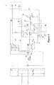
- Fig. 3 is a detailed circuit diagram of the power factor correction circuit shown in Fig. 2 . As shown in Fig. 3 , the first feedback loop 50 and the second feedback loop 60 are connected in parallel between the sample terminal SP and the feedback terminal FB.
- the switch converter circuit 20 comprises a switch Q1 and a converter 201.
- the switch Q1 is a P channel enhancement type field effect transistor that has a gate in connection with the control terminal of the controller 40, and a base and a source connected together to be in connection with the rectifier bridge 10.
- the converter 201 comprises a primary winding P1 and a secondary winding S1.
- the primary winding P1 has one terminal in connection with an output terminal of the rectifier bridge 10 and the other terminal in connection with a drain of the switch Q1, and the secondary winding S1 has one terminal in connection with a positive terminal of the LED load and the other terminal in connection with a negative terminal of the LED load.
- the first feedback loop 50 comprises an operational amplifier X1 that has a non-inverting input in connection with the sample terminal SP; a compensating network 51 that is connected between an inverting input and an output of the operational amplifier X1; and a resistor R9 that has one end in connection between the inverting input of the operational amplifier X1 and the compensating network 51, wherein the compensating network 51 and the resistor R9 jointly constitute a first feedback network.
- the compensating network 51 is formed by serially connecting a resistor R2 and a capacitor C4 and then connecting them with a capacitor C3 in parallel.
- the second feedback loop 60 comprises an operational amplifier X2 that has a non-inverting input in connection with the sample terminal SP; a compensating network 61 that is connected between an inverting input and an output of the operational amplifier X2; and a resistor R10 that has one end in connection with an inverting input of the operational amplifier X2 and the other end in connection with the other end of the resistor R9, wherein the compensating network 61 and the resistor R10 jointly constitute a second feedback network.
- the compensating network 61 is formed by a capacitor C8.
- the power factor correction circuit 1 further comprises diodes D2 and D8 as switch means, wherein an anode of the diode D2 is in connection with the output terminal of the first feedback loop 50, a cathode of the diode D8 is in connection with the output terminal of the second feedback loop 60, and cathodes of the diodes D2 and D8 are connected with each other and then coupled to the feedback terminal FB of the controller 40.
- the cathodes of the diodes D2 and D8 are connected to the feedback terminal FB of the controller 40 through an optical coupler 70.
- the first feedback loop 50 and the second feedback loop 60 are such configured that a bandwidth of the second feedback loop 60 is far greater than that of the first feedback loop 50, and the first feedback loop 50 and the second feedback loop 60 are configured in such a manner that a gain of the first feedback loop 50 is greater than that of the second feedback loop 60 in a normal and stable operation state of the power factor correction circuit 1.
- the bandwidth of the first feedback loop 50 is 1/(2 ⁇ R 2 C 3 ), and the bandwidth of the second feedback circuit 60 is 1/(2 ⁇ R 10 C 8 ).
- the bandwidth of the first feedback loop 50 can be set to be 40-60Hz, and the bandwidth of the second feedback loop 60 can be set to be thousands of hertz by configuring parameters of the resistive elements R2 and R10 and the capacitive elements C3 and C8.
- the gain of the first feedback loop 50 is ensured to be greater than that of the second feedback loop 60 by setting the parameters of various resistive elements and capacitive elements.
- the diode D2 can be assured to be forwardly conducted and the diode D8 is reversely cut off in the stable operation state of the power factor correction circuit 1, so that the controller 40 only receives the feedback signal generated by the first feedback loop 50 in the normal and stable operation state, and since the first feedback loop 50 is set to have a very slow control speed and a narrow bandwidth, the high power factor of the power factor correction circuit 1 and substantially constant control of the current output to the load can be realized.
- the bandwidth of the first feedback loop is set to be tens of hertz and the bandwidth of the second feedback loop 60 is set to be thousands of hertz
- the diode D8 is forwardly conducted and the diode D2 is reversely cut off since the voltage output from the first feedback loop 50 is greater than the voltage output from the second feedback loop 60, thus, the controller 40 only receives the feedback signal generated by the second feedback loop 60.
- the second feedback loop 60 Since the bandwidth of the second feedback loop 60 is set to be thousands of hertz, even if in the start-up period of about 20ms, the second feedback loop 60 also can feed information about current output to the LED load back to the controller 40, so that the controller can control the switch Q1 using the feedback signal received from the second feedback loop 60 so as to control the current output to the LED load, such that damage to the LED load caused by overcurrent during start-up can be avoided.
- a resistor R1 connected between the LED load and second coil S1 is a sample resistor
- the voltage across the resistor R1 is input into the non-inverting input of operational amplifier X1 in the first feedback loop 50 and the non-inverting input of operational amplifier X2 in the second feedback loop 60, and is compared with the reference voltage Vref which is input into the inverting input of operational amplifier X1 in the first feedback loop 50 and the inverting input of operational amplifier X2 in the second feedback loop 60.
- the signals generated by the first feedback loop 50 and the second feedback loop 60 are output to the controller 40 after being adjusted by the first feedback network and the second feedback network, thereby achieving power factor control and constant current control and limiting the current output to the load 30.
- a resistor R8 and a capacitor C6 form a filter network, such that the signal received by the first feedback loop 50 is a low-frequency signal, thereby achieving power factor control in the normal and stable operation state.
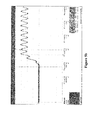
- Fig. 4 is an output voltage waveform of two feedback loops of the power factor correction circuit shown in Fig. 3 . It can be seen from Fig. 4 that a voltage signal output from the second feedback loop 60 is greater than a voltage signal of the first feedback loop 50 during the start-up period, thus, at this period, the diode D8 is forwardly conducted, and the diode D2 is reversely cut off, so that only the voltage signal output from the second feedback loop 60 flows to the controller 40, and then, the controller 40 controls the switch Q1 of the switch converter circuit 20 using the feedback signal received from the second feedback loop 60 to realize quick current-limiting control output to the LED load 30. Besides, it also can be seen from Fig.
- the controller 40 controls the switch Q1 of the switch converter circuit 20 using the feedback signal received from the first feedback loop 50 to realize the power factor control and the constant control to current output to the load.
- a waveform of an output current of the power factor correction circuit in the prior art and a waveform of an output current of the power factor correction circuit of the present invention are also given, as shown in Fig. 5a and Fig. 5b .
- Fig. 5a and Fig. 5b it can be seen from Fig. 5a and Fig. 5b that overshoot exists in the output current of the power factor correction circuit in the prior art during the start-up time, and in the output current of the power factor correction circuit according to one embodiment of the present invention, the output current during the start-up and the output current in the stable operation state are approximately equal and overshoot current is not output. Therefore, the power factor correction circuit according to one embodiment of the present invention can avoid damage to the LED load by the overcurrent in the start-up.
- the controller 40 is a PWM controller that realizes control to the switch Q1 of the switch converter circuit 20 by controlling a duty cycle of a pulse output.
- the compensating network 51 and the compensating network 61 can have multiple variations, and they can be formed by serially connecting capacitor and resistor as long as it is assured that the gain of the first feedback loop is greater than that of the second feedback loop, the bandwidth of the first feedback loop is tens of hertz, and the bandwidth of the second feedback loop is thousands of hertz.
- transistors and MOSFETs can be used to replace diodes D2 and D8 to play as the switch means, and the specific configuration mode would easily occur to the person normally skilled in the art according to the teaching of the present invention, and unnecessary details will not be given herein.
- the power factor correction circuit above can be applied to a driver for driving an LED load.
- the driver can avoid damage to the LED load due to overcurrent in the start-up while being capable of realizing the high power factor.
Landscapes
- Engineering & Computer Science (AREA)
- Power Engineering (AREA)
- Rectifiers (AREA)
- Dc-Dc Converters (AREA)
Abstract
Description
- The present invention relates to a power factor correction circuit, and in particular, to a power factor correction circuit that can quickly perform current control and a driver comprising the power factor correction circuit.
- The single stage power factor correction circuit (PFC) topology becomes popular due to its advantages of a low cost and a high efficiency, and then the single stage power factor correction circuit is used more and more in LED drivers. However, the single stage PFC topology has some shortcomings of high ripple currents and big inrush output current in start-up. Specifically, as shown in
Fig. 1a andFig. 1b , the single stage PFC topology needs to both ensure a high power factor and convert for a constant current output, as a result, the response speed of a feedback loop 50' of the PFC circuit has to be sacrificed, such that a bandwidth of a normal loop is set to be less than two times of the main frequency, for instance, in a situation that there is a 230V/50Hz main input, the bandwidth should be under 100Hz, and when margin and stability are also taken into consideration, it is about 40-60Hz. Such feedback loop having a slow response speed can be called slow feedback loop, as shown inFig. 1a andFig. 1b . A very slow response speed means that a current output in start-up is out of control because the start-up action is often completed within 20ms and a loop response speed is about 20ms, so that in a time period of 0-20ms of the start-up, a current output to a load cannot be controlled, therefore, there is a big possibility for occurrence of phenomenon of damage to LED due to overcurrent caused by inrush current generated at an output side in start-up. - In order to solve the above problem, one object of the present invention lies in providing a power factor correction circuit that can quickly perform current control. Such power factor correction circuit uses a double feedback loop control technology and can realize the quick control of an output current so as to solve the problem that an LED might be damaged due to a too big inrush current in start-up.
- The power factor correction circuit according to the present invention comprises: a rectifier bridge; a switch converter circuit having an input terminal in connection with an output terminal of the rectifier bridge; a load in connection with an output terminal of the switch converter circuit; a controller having a control terminal and a feedback terminal, the control terminal being in connection with a controlled terminal of the switch converter circuit, characterized by further comprising a first feedback loop and a second feedback loop that are in connection with a sample terminal of the switch converter circuit, the first feedback loop and the second feedback loop being such configured that the feedback terminal of the controller only receives a first feedback signal generated by the first feedback loop in a normal operation state of the power factor correction circuit, and the feedback terminal of the controller only receives a second feedback signal generated by the second feedback loop in a start-up state of the power factor correction circuit, and a bandwidth of the second feedback loop is greater than a bandwidth of the first feedback loop.
- The concept of the present invention lies in: changing that a conventional single stage power factor correction circuit only comprises a single feedback loop, a power factor correction controller can be controlled through a feedback signal generated by the feedback circuit so as to realize constant control to a current output to a load, but in order to meet requirement of a high power factor of the power factor circuit, a bandwidth of the feedback loop is often 40-60Hz, and then a response speed thereof is very slow, and a current output in a start-up state is out of control, therefore, the power factor correction circuit is configured to comprise two feedback loops, i.e. a slow feedback loop and a fast feedback loop. The slow feedback loop is functionally identical as the conventional slow feedback loop as mentioned above, while the newly added quick feedback loop is configured to allow the power factor correction circuit to control the current output to the load in the start-up using a feedback signal generated thereby, so as to avoid damage to the load by overcurrent in the start-up.
- Besides, the quick feedback loop and the slow feedback loop are such configured that the feedback terminal of the controller only receives the first feedback signal generated by the slow feedback loop in the normal operation state of the power factor correction circuit, and the feedback terminal of the controller only receives the second feedback signal generated by the quick feedback loop in the start-up state of the power factor correction circuit, i.e. feedback signals fed back to the feedback terminal of the controller are switched between the quick feedback loop and the slow feedback loop, so that a current-limiting control to a current output to the load in the start-up can be realized while assuring a high power factor of the power factor correction circuit and realizing the constant control to the current output to the load, therefore, the damage to the load due to overcurrent in the start-up can be avoided.
- In one preferred embodiment according to the present invention, the second feedback loop and the first feedback loop are connected in parallel between the sample terminal and the feedback terminal. Through such configuration, it can be realized with a simple circuit structure that a feedback signal fed back to the feedback terminal of the controller is a signal generated by the quick feedback loop in the start-up and a signal generated by the slow feedback loop in the normal operation state, so that the cost is low.
- In one preferred embodiment according to the present invention, the first feedback loop and the second feedback loop are such configured that a gain of the first feedback loop is greater than a gain of the second feedback loop. By configuring the first feedback loop and the second feedback loop in such a manner that the gain of the first feedback loop is greater than the gain of the second feedback loop, it is realized that the feedback terminal of the controller only receives the first feedback signal generated by the first feedback loop in the normal operation state of the power factor correction circuit, and thus, a gain ratio is used to control whether signals of the two feedback loops can be received by the feedback terminal of the controller, the circuit configuration can be simplified, the design is simple and easy, and it is convenient for control.
- In one preferred embodiment according to the present invention, a bandwidth of the first feedback loop is 40-60Hz, and a bandwidth of the second feedback loop is of kHz magnitude. Through such configuration, in a situation that a power voltage supplied by a power supply is 230V/50Hz, the high power factor of the power factor correction circuit and the constant control to the current output to the load can be realized in the normal operation state by using the first feedback loop, and the current-limiting control to the current output to the load during the period of start-up is realized in a situation that the start-up of the power factor correction circuit has a duration of 20ms by using the second feedback loop.
- In one preferred embodiment according to the present invention, the first feedback loop comprises a first operational amplifier; and a first feedback network comprising a first compensating network that is connected between an inverting input and an output of the first operational amplifier and a first resistive element that has one end in connection with the inverting input of the first operational amplifier and the first compensating network. By configuring the first resistive element in the first feedback loop in such a manner, an pole of the gain of the first feedback loop can be assured so that the gain ratio of gains of the first feedback loop to the second feedback loop can be easily adjusted.
- In one preferred embodiment according to the present invention, the second feedback loop comprises a second operational amplifier; and a second feedback network comprising a second compensating network that is connected between an inverting input and an output of the second operational amplifier and a second resistive element that has one end in connection with the inverting input of the second operational amplifier and the second compensating network and the other end in connection with the first resistive element. Through such configuration of the second feedback loop, the second feedback loop can be assured to be capable of feeing a high-frequency signal output to the load back to the feedback terminal of the controller, such that the controller can adjust the current output to the load more precisely, and meanwhile, such configuration of the second resistive element in the second feedback loop can assure an pole of the gain of the second feedback loop so that the gain ratio of the two feedback loops can be easily adjusted.
- In one preferred embodiment according to the present invention, the first compensating network is formed by serially connecting a third resistive element and a first capacitive element and then connecting them with a second capacitive element in parallel, and the second compensating network is formed by a third capacitive element. Through such configuration, the first feedback loop can be allowed to feed a low-frequency component in a signal output to the load back to the controller, and the second feedback loop can be allowed to feed a high-frequency component in a signal output to the load back to the controller, so that the high power factor and more precise control to the current output to the load can be realized. In addition, the first compensating network and the second compensating network also can have other forms as long as the bandwidth of the first feedback loop is 40-60Hz, the bandwidth of the second feedback loop is of kHz magnitude, and the gain of the first feedback loop is greater than the gain of the second feedback loop.
- In one preferred embodiment according to the present invention, switch means are further comprised. By using the switch means, only the second feedback signal is allowed to be fed back to the feedback terminal of the controller in the start-up state and only the first feedback signal is allowed to be fed back to the feedback terminal of the controller in the normal operation state. To enable the feedback signals generated by different feedback loops in different states to flow to the feedback terminal of the controller, by using the switch means, is characterized with a simple design, easy accomplishment and a low cost.
- In one preferred embodiment according to the present invention, the switch means comprise a first switch and a second switch, the first switch is connected between an output terminal of the first feedback loop and the feedback terminal of the controller, and the second switch is connected between an output terminal of the second feedback loop and the feedback terminal of the controller. Through such configuration, it can be realized that in the start-up state, the first switch is disabled and the second switch is enabled such that only the feedback signal generated by the second feedback loop is fed back to the feedback terminal of the controller, and in the normal operation state, the first switch is enabled and the second switch is disabled such that only the feedback signal generated by the first feedback loop is fed back to the feedback terminal of the controller, thus, the implementation method is simple and easy to use. Preferably, the first switch and the second switch are diodes, transistors or MOSFETs.
- In one preferred embodiment according to the present invention, the switch converter circuit comprises a converter having a primary side unit and a secondary side unit, and input terminals of the first feedback loop and the second feedback loop are connected to the secondary side unit. Through such configuration, the first feedback loop and the second feedback loop can be allowed to sample the signal output by the switch converter circuit to the load to realize control to the current output to the load and control of the power factor. The design is simple and easy to use.
- In one preferred embodiment according to the present invention, the switch converter circuit further comprises a third switch, a control electrode of the third switch is used as the controlled terminal of the switch converter circuit, and a working electrode of the third switch is connected with one input terminal of the primary side unit, and the other input terminal of the primary side unit is connected to the rectifier bridge. Through such configuration, a duty cycle of on and off of the third switch can be controlled by using a PWM controller, i.e. by adjusting a duty cycle of a pulse signal output by the PWM controller to the control electrode of the third switch, so as to realize control to the power factor and control to the current output to the load. The structure is simple and precise control can be performed.
- The other object of the present invention lies in providing a driver comprising the power factor correction circuit according to any of the above. In a situation that the driver comprises the above power factor correction circuit, the driver can avoid damage to the load due to overcurrent in the start-up while being capable of realizing the high power factor.
- The power factor correction circuit according to the present invention can assure that the load is not damaged by overcurrent in the start-up in a precondition that the high power factor can be assured.
- The accompanying drawings constitute a part of the present Description and are used to provide further understanding of the present invention. Such accompanying drawings illustrate the embodiments of the present invention and are used to describe the principles of the present invention together with the Description. In the accompanying drawings the same components are represented by the same reference numbers. As shown in the drawings:
-
Fig. 1a is a block diagram of a power factor correction circuit in the part art, andFig. 1b is a schematic circuit diagram of the power factor correction circuit shown inFig. 1a ; -
Fig. 2 is a block diagram of a first embodiment of a power factor correction circuit according to the present invention; -
Fig. 3 is a detailed circuit diagram of the power factor correction circuit shown inFig. 2 ; -
Fig. 4 is an output voltage waveform of two feedback loops of the power factor correction circuit shown inFig. 3 ; and -
Fig. 5a andFig. 5b are a waveform of an output current of the power factor correction circuit shown inFig. 1b and a waveform of an output current of the power factor correction circuit shown inFig. 3 , respectively. -
Fig. 2 is a block diagram of a first embodiment of a power factor correction circuit according to the present invention. As shown inFig. 2 , a powerfactor correction circuit 1 comprises arectifier bridge 10 that receives a power from a power supply (not shown) and rectifies the power received; aswitch converter circuit 20 that has an input terminal in connection with an output terminal of therectifier bridge 10 and is configured to receive the power from therectifier bridge 10 and to convert the power; aload 30 that is connected to an output terminal of theswitch converter circuit 20 to receive the power for operation from theswitch converter circuit 20; acontroller 40 that has a control terminal in connection with a switch (not shown) of theswitch converter circuit 20 for controlling on and off of theswitch converter circuit 20 to realize power factor correction control and control of a current output to the load; afirst feedback loop 50 that has an input terminal in connection with a sample terminal of theswitch converter circuit 20 and an output terminal in communication with a feedback terminal of thecontroller 40; and asecond feedback loop 60 that has an input terminal in connection with the sample terminal of theswitch converter circuit 20 and an output terminal in communication with the feedback terminal of thecontroller 40. - Specifically, when the power
factor correction circuit 1 is in a normal and stable operation state, only a first feedback signal S5 generated by thefirst feedback loop 50 can flow to thecontroller 40, while thesecond feedback loop 60 serves no function, at which time, in order to realize a high power factor of the powerfactor correction circuit 1, thefirst feedback loop 50 is set to have a quite slow control speed and a narrow bandwidth (less than two times of power frequency, about 40-60Hz), so that thefirst feedback loop 50 is further allowed to be capable of realizing substantially constant control of the current output to the load. Thefirst feedback loop 50 is also called a slow feedback loop. - when the power
factor correction circuit 1 is stated up, only the second feedback signal S6 generated by thesecond feedback loop 60 can flow to thecontroller 40, while thefirst feedback loop 60 serves no function. Specifically, When the powerfactor correction circuit 1 is started up, a current sample signal sampled by the sample terminal suddenly increases, and as a duration of start-up is about 20ms, the start-up, an input trend, requires a quick response, which demands thesecond feedback loop 60 to have a quick control speed and a wider bandwidth than that of thefirst feedback loop 50. In the text, the current output to the load during start-up is quickly controlled by configuring thesecond feedback loop 60 to have a bandwidth of thousands of hertz. In addition, thesecond feedback loop 60 is also called a quick feedback loop. - In the present embodiment, the power
factor correction circuit 1 is configured to comprise two feedback loops, i.e. thefirst feedback loop 50 and thesecond feedback loop 60, wherein in the normal and stable operation state of the powerfactor correction circuit 1, thecontroller 40 controls theswitch converter circuit 20, using a control signal received from thefirst feedback loop 50, to supply to LED load a current for stable and normal operation, and in a start-up state of the powerfactor correction circuit 1, thecontroller 40 controls theswitch converter circuit 20, using a feedback signal received from thesecond feedback loop 60, to realize quick control to the current output to theload 30, that is, through configuration of a quick feedback loop and a slow feedback loop in the powerfactor correction circuit 1, the problem of inrush current at an output side in the start-up cannot be controlled due to the slow response speed of the feedback loop in the prior art can be solved, while the power factor control and the constant control to the current output to the load can be realized. -
Fig. 3 is a detailed circuit diagram of the power factor correction circuit shown inFig. 2 . As shown inFig. 3 , thefirst feedback loop 50 and thesecond feedback loop 60 are connected in parallel between the sample terminal SP and the feedback terminal FB. - As shown in
Fig. 3 , theswitch converter circuit 20 comprises a switch Q1 and aconverter 201. The switch Q1 is a P channel enhancement type field effect transistor that has a gate in connection with the control terminal of thecontroller 40, and a base and a source connected together to be in connection with therectifier bridge 10. Theconverter 201 comprises a primary winding P1 and a secondary winding S1. The primary winding P1 has one terminal in connection with an output terminal of therectifier bridge 10 and the other terminal in connection with a drain of the switch Q1, and the secondary winding S1 has one terminal in connection with a positive terminal of the LED load and the other terminal in connection with a negative terminal of the LED load. Thefirst feedback loop 50 comprises an operational amplifier X1 that has a non-inverting input in connection with the sample terminal SP; a compensating network 51 that is connected between an inverting input and an output of the operational amplifier X1; and a resistor R9 that has one end in connection between the inverting input of the operational amplifier X1 and the compensating network 51, wherein the compensating network 51 and the resistor R9 jointly constitute a first feedback network. In the present embodiment, the compensating network 51 is formed by serially connecting a resistor R2 and a capacitor C4 and then connecting them with a capacitor C3 in parallel. Thesecond feedback loop 60 comprises an operational amplifier X2 that has a non-inverting input in connection with the sample terminal SP; a compensating network 61 that is connected between an inverting input and an output of the operational amplifier X2; and a resistor R10 that has one end in connection with an inverting input of the operational amplifier X2 and the other end in connection with the other end of the resistor R9, wherein the compensating network 61 and the resistor R10 jointly constitute a second feedback network. In the present embodiment, the compensating network 61 is formed by a capacitor C8. - Reference is still made to
Fig. 3 . As shown inFig. 3 , the powerfactor correction circuit 1 further comprises diodes D2 and D8 as switch means, wherein an anode of the diode D2 is in connection with the output terminal of thefirst feedback loop 50, a cathode of the diode D8 is in connection with the output terminal of thesecond feedback loop 60, and cathodes of the diodes D2 and D8 are connected with each other and then coupled to the feedback terminal FB of thecontroller 40. In the present embodiment, the cathodes of the diodes D2 and D8 are connected to the feedback terminal FB of thecontroller 40 through an optical coupler 70. - In the first embodiment, the
first feedback loop 50 and thesecond feedback loop 60 are such configured that a bandwidth of thesecond feedback loop 60 is far greater than that of thefirst feedback loop 50, and thefirst feedback loop 50 and thesecond feedback loop 60 are configured in such a manner that a gain of thefirst feedback loop 50 is greater than that of thesecond feedback loop 60 in a normal and stable operation state of the powerfactor correction circuit 1. - Specifically, in the present embodiment, the bandwidth of the
first feedback loop 50 is 1/(2πR2C3), and the bandwidth of thesecond feedback circuit 60 is 1/(2πR10C8). The bandwidth of thefirst feedback loop 50 can be set to be 40-60Hz, and the bandwidth of thesecond feedback loop 60 can be set to be thousands of hertz by configuring parameters of the resistive elements R2 and R10 and the capacitive elements C3 and C8. The gain of thefirst feedback loop 50 is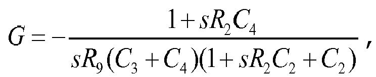
second feedback loop 60 is
first feedback loop 50 is ensured to be greater than that of thesecond feedback loop 60 by setting the parameters of various resistive elements and capacitive elements. - Through the above configuration, the diode D2 can be assured to be forwardly conducted and the diode D8 is reversely cut off in the stable operation state of the power
factor correction circuit 1, so that thecontroller 40 only receives the feedback signal generated by thefirst feedback loop 50 in the normal and stable operation state, and since thefirst feedback loop 50 is set to have a very slow control speed and a narrow bandwidth, the high power factor of the powerfactor correction circuit 1 and substantially constant control of the current output to the load can be realized. - In addition, through the above configuration, in the start-up state of the power
factor correction circuit 1, since the bandwidth of the first feedback loop is set to be tens of hertz and the bandwidth of thesecond feedback loop 60 is set to be thousands of hertz, during the start-up period of about 20ms, as a voltage output from thefirst feedback loop 50 rises slowly and a voltage output from thesecond feedback loop 60 rises quickly, at this time, the diode D8 is forwardly conducted and the diode D2 is reversely cut off since the voltage output from thefirst feedback loop 50 is greater than the voltage output from thesecond feedback loop 60, thus, thecontroller 40 only receives the feedback signal generated by thesecond feedback loop 60. Since the bandwidth of thesecond feedback loop 60 is set to be thousands of hertz, even if in the start-up period of about 20ms, thesecond feedback loop 60 also can feed information about current output to the LED load back to thecontroller 40, so that the controller can control the switch Q1 using the feedback signal received from thesecond feedback loop 60 so as to control the current output to the LED load, such that damage to the LED load caused by overcurrent during start-up can be avoided. - It should be understood that in the power factor correction circuit shown in
Fig. 3 , a resistor R1 connected between the LED load and second coil S1 is a sample resistor, the voltage across the resistor R1 is input into the non-inverting input of operational amplifier X1 in thefirst feedback loop 50 and the non-inverting input of operational amplifier X2 in thesecond feedback loop 60, and is compared with the reference voltage Vref which is input into the inverting input of operational amplifier X1 in thefirst feedback loop 50 and the inverting input of operational amplifier X2 in thesecond feedback loop 60. The signals generated by thefirst feedback loop 50 and thesecond feedback loop 60 are output to thecontroller 40 after being adjusted by the first feedback network and the second feedback network, thereby achieving power factor control and constant current control and limiting the current output to theload 30. - It should be noted that, a resistor R8 and a capacitor C6 form a filter network, such that the signal received by the
first feedback loop 50 is a low-frequency signal, thereby achieving power factor control in the normal and stable operation state. - In addition,
Fig. 4 is an output voltage waveform of two feedback loops of the power factor correction circuit shown inFig. 3 . It can be seen fromFig. 4 that a voltage signal output from thesecond feedback loop 60 is greater than a voltage signal of thefirst feedback loop 50 during the start-up period, thus, at this period, the diode D8 is forwardly conducted, and the diode D2 is reversely cut off, so that only the voltage signal output from thesecond feedback loop 60 flows to thecontroller 40, and then, thecontroller 40 controls the switch Q1 of theswitch converter circuit 20 using the feedback signal received from thesecond feedback loop 60 to realize quick current-limiting control output to theLED load 30. Besides, it also can be seen fromFig. 4 that in a normal and stable operation period, the voltage signal output from thesecond feedback loop 60 is less than the voltage signal output from thefirst feedback loop 50, thus at this period, the diode D5 is reversely cut off and the diode D2 is forwardly conducted, so that only the voltage signal output from thefirst feedback loop 50 flows to thecontroller 40, and then thecontroller 40 controls the switch Q1 of theswitch converter circuit 20 using the feedback signal received from thefirst feedback loop 50 to realize the power factor control and the constant control to current output to the load. - For the sake of easy understanding, a waveform of an output current of the power factor correction circuit in the prior art and a waveform of an output current of the power factor correction circuit of the present invention are also given, as shown in
Fig. 5a andFig. 5b . It can be seen fromFig. 5a andFig. 5b that overshoot exists in the output current of the power factor correction circuit in the prior art during the start-up time, and in the output current of the power factor correction circuit according to one embodiment of the present invention, the output current during the start-up and the output current in the stable operation state are approximately equal and overshoot current is not output. Therefore, the power factor correction circuit according to one embodiment of the present invention can avoid damage to the LED load by the overcurrent in the start-up. - It should be noted that in the present embodiment, the
controller 40 is a PWM controller that realizes control to the switch Q1 of theswitch converter circuit 20 by controlling a duty cycle of a pulse output. - In another embodiment of the power factor correction circuit according to the present invention, the compensating network 51 and the compensating network 61 can have multiple variations, and they can be formed by serially connecting capacitor and resistor as long as it is assured that the gain of the first feedback loop is greater than that of the second feedback loop, the bandwidth of the first feedback loop is tens of hertz, and the bandwidth of the second feedback loop is thousands of hertz.
- In another embodiment of the power factor correction circuit according to the present invention, transistors and MOSFETs can be used to replace diodes D2 and D8 to play as the switch means, and the specific configuration mode would easily occur to the person normally skilled in the art according to the teaching of the present invention, and unnecessary details will not be given herein.
- The power factor correction circuit above can be applied to a driver for driving an LED load. In a situation that the driver has the above power factor correction circuit, the driver can avoid damage to the LED load due to overcurrent in the start-up while being capable of realizing the high power factor.
- The above is merely preferred embodiments of the present invention but not to limit the present invention. For the person skilled in the art, the present invention may have various alterations and changes. Any alterations, equivalent substitutions, improvements, within the spirit and principle of the present invention, should be covered in the protection scope of the present invention.
Claims (13)
- A power factor correction circuit (1) comprising: a rectifier bridge (10); a switch converter circuit (20) having an input terminal in connection with an output terminal of the rectifier bridge (10); a load (30) in connection with an output terminal of the switch converter circuit (20); a controller (40) having a control terminal and a feedback terminal (FB), the control terminal being in connection with a controlled terminal of the switch converter circuit (20), characterized by further comprising a first feedback loop (50) and a second feedback loop (60) that are in connection with a sample terminal (SP) of the switch converter circuit (20), the first feedback loop (50) and the second feedback loop (60) being configured such that the feedback terminal (FB) of the controller (40) only receives a first feedback signal (S5) generated by the first feedback loop (50) in a normal operation state of the power factor correction circuit (1), and the feedback terminal (FB) of the controller (40) only receives a second feedback signal (S6) generated by the second feedback loop (60) in a start-up state of the power factor correction circuit (1), and a bandwidth of the second feedback loop (60) is greater than a bandwidth of the first feedback loop (50).
- The power factor correction circuit according to Claim 1, characterized in that the second feedback loop (60) and the first feedback loop (50) are connected in parallel between the sample terminal (SP) and the feedback terminal (FB).
- The power factor correction circuit according to Claim 1, characterized in that the first feedback loop (50) and the second feedback loop (60) are configured such that a gain of the first feedback loop (50) is greater than that of the second feedback loop (60).
- The power factor correction circuit according to any of Claims 1-3, characterized in that a bandwidth of the first feedback loop (50) is 40-60Hz, and a bandwidth of the second feedback loop (60) is of kHz magnitude.
- The power factor correction circuit according to Claim 1, characterized in that the first feedback loop (50) comprises a first operational amplifier (X1); and a first feedback network comprising a first compensating network (51) that is connected between an inverting input and an output of the first operational amplifier (X1) and a first resistive element (R9) that has one end in connection with the inverting input of the first operational amplifier (X1) and the first compensating network (51).
- The power factor correction circuit according to Claim 5, characterized in that the second feedback loop (60) comprises a second operational amplifier (X2); and a second feedback network comprising a second compensating network (61) that is connected between an inverting input and an output of the second operational amplifier (X2) and a second resistive element (R10) that has one end in connection with the inverting input of the second operational amplifier (X2) and the second compensating network (61) and the other end in connection with the first resistive element (R9).
- The power factor correction circuit according to Claim 5 or 6, characterized in that the first compensating network (51) is formed by serially connecting a third resistive element (R2) and a first capacitive element (C4) and then connecting them with a second capacitive element (C3) in parallel, and the second compensating network is formed by a third capacitive element (C8).
- The power factor correction circuit according to Claim 1, characterized by further comprising switch means (D2, D8), by using which only the second feedback signal (S6) is allowed to be fed back to the feedback terminal (FB) of the controller (40) in the start-up state and only the first feedback signal (S5) is allowed to be fed back to the feedback terminal (FB) of the controller (40) in the normal operation state.
- The power factor correction circuit according to Claim 8, characterized in that the switch means comprise a first switch (D2) and a second switch (D8), the first switch (D2) is connected between an output terminal of the first feedback loop (50) and the feedback terminal (FB) of the controller (40), and the second switch (D8) is connected between an output terminal of the second feedback loop (60) and the feedback terminal (FB) of the controller (40).
- The power factor correction circuit according to Claim 9, characterized in that the first switch (D2) and the second switch (D8) are diodes, transistors or MOSFETs.
- The power factor correction circuit according to Claim 1, characterized in that the switch converter circuit (20) comprises a converter (201) having a primary side unit (P1) and a secondary side unit (S1), and input terminals of the first feedback loop (50) and the second feedback loop (60) are coupled to the secondary side unit (S1).
- The power factor correction circuit according to Claim 11, characterized in that the switch converter circuit (20) further comprises a third switch (Q1), a control electrode of the third switch (Q1) is used as the controlled terminal of the switch converter circuit (20), and a working electrode of the third switch (Q1) is connected with one input terminal of the primary side unit (P1), and the other input terminal of the primary side unit (P1) is connected to the rectifier bridge (10).
- A driver comprising the power factor correction circuit according to any of Claims 1-12.
Applications Claiming Priority (1)
| Application Number | Priority Date | Filing Date | Title |
|---|---|---|---|
| CN201210320911.3A CN103683894B (en) | 2012-08-31 | 2012-08-31 | Circuit of power factor correction and the driver comprising the circuit of power factor correction |
Publications (3)
| Publication Number | Publication Date |
|---|---|
| EP2704531A2 true EP2704531A2 (en) | 2014-03-05 |
| EP2704531A3 EP2704531A3 (en) | 2017-06-21 |
| EP2704531B1 EP2704531B1 (en) | 2018-10-10 |
Family
ID=49033980
Family Applications (1)
| Application Number | Title | Priority Date | Filing Date |
|---|---|---|---|
| EP13181906.2A Not-in-force EP2704531B1 (en) | 2012-08-31 | 2013-08-27 | Power factor correction circuit and driver comprising the power factor correction circuit |
Country Status (2)
| Country | Link |
|---|---|
| EP (1) | EP2704531B1 (en) |
| CN (1) | CN103683894B (en) |
Cited By (2)
| Publication number | Priority date | Publication date | Assignee | Title |
|---|---|---|---|---|
| CN115804001A (en) * | 2020-06-16 | 2023-03-14 | 红色半导体公司 | Power converter, controller and method |
| CN117130453A (en) * | 2023-08-31 | 2023-11-28 | 联想(北京)有限公司 | A control method, power supply module and electronic device |
Family Cites Families (9)
| Publication number | Priority date | Publication date | Assignee | Title |
|---|---|---|---|---|
| WO2006059583A1 (en) * | 2004-12-03 | 2006-06-08 | Matsushita Electric Works, Ltd. | Electric discharge lamp operation device and illumination instrument |
| US7378805B2 (en) * | 2005-03-22 | 2008-05-27 | Fairchild Semiconductor Corporation | Single-stage digital power converter for driving LEDs |
| US7446517B2 (en) * | 2006-01-26 | 2008-11-04 | Semiconductor Components Industries L.L.C. | Power supply controller and method therefor |
| JP4389914B2 (en) * | 2006-09-19 | 2009-12-24 | 船井電機株式会社 | Light source lighting device |
| CN201409085Y (en) * | 2009-03-31 | 2010-02-17 | 深圳市欧美亚实业有限公司 | DC boost converter |
| US8547033B2 (en) * | 2010-10-05 | 2013-10-01 | Microsemi Corp.—Analog Mixed Signal Group Ltd. | LED string driver with power factor corrector and current governor |
| KR101057684B1 (en) * | 2011-03-31 | 2011-08-18 | 주식회사 동운아나텍 | Lighting drive |
| CN202059322U (en) * | 2011-04-23 | 2011-11-30 | 瑞谷科技(深圳)有限公司 | Anti-inductance-saturation power converter |
| CN102186292B (en) * | 2011-04-30 | 2013-09-18 | 杭州电子科技大学 | Primary edge current reference generating circuit and method for high power factor constant-current switch power supply |
-
2012
- 2012-08-31 CN CN201210320911.3A patent/CN103683894B/en not_active Expired - Fee Related
-
2013
- 2013-08-27 EP EP13181906.2A patent/EP2704531B1/en not_active Not-in-force
Non-Patent Citations (1)
| Title |
|---|
| None |
Cited By (4)
| Publication number | Priority date | Publication date | Assignee | Title |
|---|---|---|---|---|
| CN115804001A (en) * | 2020-06-16 | 2023-03-14 | 红色半导体公司 | Power converter, controller and method |
| US20230246543A1 (en) * | 2020-06-16 | 2023-08-03 | Redisem Ltd. | Power Converter, Controller, and Methods |
| US12438451B2 (en) * | 2020-06-16 | 2025-10-07 | Redisem Ltd. | Power converter, controller, and methods |
| CN117130453A (en) * | 2023-08-31 | 2023-11-28 | 联想(北京)有限公司 | A control method, power supply module and electronic device |
Also Published As
| Publication number | Publication date |
|---|---|
| EP2704531A3 (en) | 2017-06-21 |
| CN103683894B (en) | 2017-12-26 |
| CN103683894A (en) | 2014-03-26 |
| EP2704531B1 (en) | 2018-10-10 |
Similar Documents
| Publication | Publication Date | Title |
|---|---|---|
| KR102282142B1 (en) | How to reduce transformer circuit and no-load power consumption | |
| CN104010406B (en) | Led driver | |
| US20200052598A1 (en) | Voltage sense control circuit, voltage sense control method and isolated converter thereof | |
| TW201535943A (en) | Method of forming a power supply controller and structure therefor | |
| JP2012216536A (en) | Light driving apparatus | |
| JP4787350B2 (en) | Self-excited switching power supply circuit | |
| CN102130614A (en) | A multi-channel output switching power supply circuit and its switching power supply and device | |
| KR20100023770A (en) | Circuit arrangement for operating at least one semiconductor light source | |
| JP2000278945A (en) | Switching power supply | |
| CN102474190A (en) | Charging device for charging a battery pack | |
| CN102013800B (en) | Power conversion device | |
| US20200389093A1 (en) | Switched mode power converter and conversion method | |
| CN110943499A (en) | Novel energy storage circuit | |
| US9190914B2 (en) | Switching power supply apparatus | |
| JP2006136146A (en) | Switching power supply | |
| US20150078040A1 (en) | Isolated switching power supply | |
| JP2016063732A (en) | Switching power supply | |
| EP2704531B1 (en) | Power factor correction circuit and driver comprising the power factor correction circuit | |
| CN103516218B (en) | Power supply device | |
| JP5545839B2 (en) | Switching power supply | |
| US10320194B2 (en) | Control feedback loop design with fast transient response for multi-level converter | |
| CN215120575U (en) | Voltage stabilizing circuit applied to flyback power supply and television | |
| JP6867941B2 (en) | Switching power supply | |
| JP5861314B2 (en) | DC-DC converter | |
| JP2007159305A (en) | Power supply |
Legal Events
| Date | Code | Title | Description |
|---|---|---|---|
| AK | Designated contracting states |
Kind code of ref document: A2 Designated state(s): AL AT BE BG CH CY CZ DE DK EE ES FI FR GB GR HR HU IE IS IT LI LT LU LV MC MK MT NL NO PL PT RO RS SE SI SK SM TR |
|
| AX | Request for extension of the european patent |
Extension state: BA ME |
|
| PUAI | Public reference made under article 153(3) epc to a published international application that has entered the european phase |
Free format text: ORIGINAL CODE: 0009012 |
|
| PUAL | Search report despatched |
Free format text: ORIGINAL CODE: 0009013 |
|
| AK | Designated contracting states |
Kind code of ref document: A3 Designated state(s): AL AT BE BG CH CY CZ DE DK EE ES FI FR GB GR HR HU IE IS IT LI LT LU LV MC MK MT NL NO PL PT RO RS SE SI SK SM TR |
|
| AX | Request for extension of the european patent |
Extension state: BA ME |
|
| RIC1 | Information provided on ipc code assigned before grant |
Ipc: H05B 33/08 20060101AFI20170517BHEP |
|
| STAA | Information on the status of an ep patent application or granted ep patent |
Free format text: STATUS: REQUEST FOR EXAMINATION WAS MADE |
|
| 17P | Request for examination filed |
Effective date: 20171221 |
|
| RBV | Designated contracting states (corrected) |
Designated state(s): AL AT BE BG CH CY CZ DE DK EE ES FI FR GB GR HR HU IE IS IT LI LT LU LV MC MK MT NL NO PL PT RO RS SE SI SK SM TR |
|
| GRAP | Despatch of communication of intention to grant a patent |
Free format text: ORIGINAL CODE: EPIDOSNIGR1 |
|
| STAA | Information on the status of an ep patent application or granted ep patent |
Free format text: STATUS: GRANT OF PATENT IS INTENDED |
|
| INTG | Intention to grant announced |
Effective date: 20180508 |
|
| RIN1 | Information on inventor provided before grant (corrected) |
Inventor name: ZHUANG, XIHE Inventor name: ZHANG, QUAN Inventor name: LIN, DAN Inventor name: WEI, ZEKE |
|
| GRAS | Grant fee paid |
Free format text: ORIGINAL CODE: EPIDOSNIGR3 |
|
| GRAA | (expected) grant |
Free format text: ORIGINAL CODE: 0009210 |
|
| STAA | Information on the status of an ep patent application or granted ep patent |
Free format text: STATUS: THE PATENT HAS BEEN GRANTED |
|
| AK | Designated contracting states |
Kind code of ref document: B1 Designated state(s): AL AT BE BG CH CY CZ DE DK EE ES FI FR GB GR HR HU IE IS IT LI LT LU LV MC MK MT NL NO PL PT RO RS SE SI SK SM TR |
|
| REG | Reference to a national code |
Ref country code: GB Ref legal event code: FG4D |
|
| REG | Reference to a national code |
Ref country code: CH Ref legal event code: EP Ref country code: AT Ref legal event code: REF Ref document number: 1052810 Country of ref document: AT Kind code of ref document: T Effective date: 20181015 |
|
| REG | Reference to a national code |
Ref country code: IE Ref legal event code: FG4D |
|
| REG | Reference to a national code |
Ref country code: DE Ref legal event code: R096 Ref document number: 602013044772 Country of ref document: DE |
|
| REG | Reference to a national code |
Ref country code: NL Ref legal event code: MP Effective date: 20181010 |
|
| REG | Reference to a national code |
Ref country code: LT Ref legal event code: MG4D |
|
| REG | Reference to a national code |
Ref country code: AT Ref legal event code: MK05 Ref document number: 1052810 Country of ref document: AT Kind code of ref document: T Effective date: 20181010 |
|
| PG25 | Lapsed in a contracting state [announced via postgrant information from national office to epo] |
Ref country code: NL Free format text: LAPSE BECAUSE OF FAILURE TO SUBMIT A TRANSLATION OF THE DESCRIPTION OR TO PAY THE FEE WITHIN THE PRESCRIBED TIME-LIMIT Effective date: 20181010 |
|
| PG25 | Lapsed in a contracting state [announced via postgrant information from national office to epo] |
Ref country code: HR Free format text: LAPSE BECAUSE OF FAILURE TO SUBMIT A TRANSLATION OF THE DESCRIPTION OR TO PAY THE FEE WITHIN THE PRESCRIBED TIME-LIMIT Effective date: 20181010 Ref country code: PL Free format text: LAPSE BECAUSE OF FAILURE TO SUBMIT A TRANSLATION OF THE DESCRIPTION OR TO PAY THE FEE WITHIN THE PRESCRIBED TIME-LIMIT Effective date: 20181010 Ref country code: NO Free format text: LAPSE BECAUSE OF FAILURE TO SUBMIT A TRANSLATION OF THE DESCRIPTION OR TO PAY THE FEE WITHIN THE PRESCRIBED TIME-LIMIT Effective date: 20190110 Ref country code: LV Free format text: LAPSE BECAUSE OF FAILURE TO SUBMIT A TRANSLATION OF THE DESCRIPTION OR TO PAY THE FEE WITHIN THE PRESCRIBED TIME-LIMIT Effective date: 20181010 Ref country code: AT Free format text: LAPSE BECAUSE OF FAILURE TO SUBMIT A TRANSLATION OF THE DESCRIPTION OR TO PAY THE FEE WITHIN THE PRESCRIBED TIME-LIMIT Effective date: 20181010 Ref country code: FI Free format text: LAPSE BECAUSE OF FAILURE TO SUBMIT A TRANSLATION OF THE DESCRIPTION OR TO PAY THE FEE WITHIN THE PRESCRIBED TIME-LIMIT Effective date: 20181010 Ref country code: BG Free format text: LAPSE BECAUSE OF FAILURE TO SUBMIT A TRANSLATION OF THE DESCRIPTION OR TO PAY THE FEE WITHIN THE PRESCRIBED TIME-LIMIT Effective date: 20190110 Ref country code: IS Free format text: LAPSE BECAUSE OF FAILURE TO SUBMIT A TRANSLATION OF THE DESCRIPTION OR TO PAY THE FEE WITHIN THE PRESCRIBED TIME-LIMIT Effective date: 20190210 Ref country code: ES Free format text: LAPSE BECAUSE OF FAILURE TO SUBMIT A TRANSLATION OF THE DESCRIPTION OR TO PAY THE FEE WITHIN THE PRESCRIBED TIME-LIMIT Effective date: 20181010 Ref country code: LT Free format text: LAPSE BECAUSE OF FAILURE TO SUBMIT A TRANSLATION OF THE DESCRIPTION OR TO PAY THE FEE WITHIN THE PRESCRIBED TIME-LIMIT Effective date: 20181010 |
|
| PG25 | Lapsed in a contracting state [announced via postgrant information from national office to epo] |
Ref country code: GR Free format text: LAPSE BECAUSE OF FAILURE TO SUBMIT A TRANSLATION OF THE DESCRIPTION OR TO PAY THE FEE WITHIN THE PRESCRIBED TIME-LIMIT Effective date: 20190111 Ref country code: PT Free format text: LAPSE BECAUSE OF FAILURE TO SUBMIT A TRANSLATION OF THE DESCRIPTION OR TO PAY THE FEE WITHIN THE PRESCRIBED TIME-LIMIT Effective date: 20190210 Ref country code: AL Free format text: LAPSE BECAUSE OF FAILURE TO SUBMIT A TRANSLATION OF THE DESCRIPTION OR TO PAY THE FEE WITHIN THE PRESCRIBED TIME-LIMIT Effective date: 20181010 Ref country code: RS Free format text: LAPSE BECAUSE OF FAILURE TO SUBMIT A TRANSLATION OF THE DESCRIPTION OR TO PAY THE FEE WITHIN THE PRESCRIBED TIME-LIMIT Effective date: 20181010 Ref country code: SE Free format text: LAPSE BECAUSE OF FAILURE TO SUBMIT A TRANSLATION OF THE DESCRIPTION OR TO PAY THE FEE WITHIN THE PRESCRIBED TIME-LIMIT Effective date: 20181010 |
|
| REG | Reference to a national code |
Ref country code: DE Ref legal event code: R097 Ref document number: 602013044772 Country of ref document: DE |
|
| PG25 | Lapsed in a contracting state [announced via postgrant information from national office to epo] |
Ref country code: DK Free format text: LAPSE BECAUSE OF FAILURE TO SUBMIT A TRANSLATION OF THE DESCRIPTION OR TO PAY THE FEE WITHIN THE PRESCRIBED TIME-LIMIT Effective date: 20181010 Ref country code: CZ Free format text: LAPSE BECAUSE OF FAILURE TO SUBMIT A TRANSLATION OF THE DESCRIPTION OR TO PAY THE FEE WITHIN THE PRESCRIBED TIME-LIMIT Effective date: 20181010 |
|
| PLBE | No opposition filed within time limit |
Free format text: ORIGINAL CODE: 0009261 |
|
| STAA | Information on the status of an ep patent application or granted ep patent |
Free format text: STATUS: NO OPPOSITION FILED WITHIN TIME LIMIT |
|
| PG25 | Lapsed in a contracting state [announced via postgrant information from national office to epo] |
Ref country code: SK Free format text: LAPSE BECAUSE OF FAILURE TO SUBMIT A TRANSLATION OF THE DESCRIPTION OR TO PAY THE FEE WITHIN THE PRESCRIBED TIME-LIMIT Effective date: 20181010 Ref country code: EE Free format text: LAPSE BECAUSE OF FAILURE TO SUBMIT A TRANSLATION OF THE DESCRIPTION OR TO PAY THE FEE WITHIN THE PRESCRIBED TIME-LIMIT Effective date: 20181010 Ref country code: SM Free format text: LAPSE BECAUSE OF FAILURE TO SUBMIT A TRANSLATION OF THE DESCRIPTION OR TO PAY THE FEE WITHIN THE PRESCRIBED TIME-LIMIT Effective date: 20181010 Ref country code: RO Free format text: LAPSE BECAUSE OF FAILURE TO SUBMIT A TRANSLATION OF THE DESCRIPTION OR TO PAY THE FEE WITHIN THE PRESCRIBED TIME-LIMIT Effective date: 20181010 |
|
| 26N | No opposition filed |
Effective date: 20190711 |
|
| PG25 | Lapsed in a contracting state [announced via postgrant information from national office to epo] |
Ref country code: SI Free format text: LAPSE BECAUSE OF FAILURE TO SUBMIT A TRANSLATION OF THE DESCRIPTION OR TO PAY THE FEE WITHIN THE PRESCRIBED TIME-LIMIT Effective date: 20181010 |
|
| REG | Reference to a national code |
Ref country code: DE Ref legal event code: R079 Ref document number: 602013044772 Country of ref document: DE Free format text: PREVIOUS MAIN CLASS: H05B0033080000 Ipc: H05B0045000000 |
|
| PG25 | Lapsed in a contracting state [announced via postgrant information from national office to epo] |
Ref country code: TR Free format text: LAPSE BECAUSE OF FAILURE TO SUBMIT A TRANSLATION OF THE DESCRIPTION OR TO PAY THE FEE WITHIN THE PRESCRIBED TIME-LIMIT Effective date: 20181010 |
|
| GBPC | Gb: european patent ceased through non-payment of renewal fee |
Effective date: 20190827 |
|
| PG25 | Lapsed in a contracting state [announced via postgrant information from national office to epo] |
Ref country code: LU Free format text: LAPSE BECAUSE OF NON-PAYMENT OF DUE FEES Effective date: 20190827 Ref country code: CH Free format text: LAPSE BECAUSE OF NON-PAYMENT OF DUE FEES Effective date: 20190831 Ref country code: LI Free format text: LAPSE BECAUSE OF NON-PAYMENT OF DUE FEES Effective date: 20190831 Ref country code: MC Free format text: LAPSE BECAUSE OF FAILURE TO SUBMIT A TRANSLATION OF THE DESCRIPTION OR TO PAY THE FEE WITHIN THE PRESCRIBED TIME-LIMIT Effective date: 20181010 |
|
| REG | Reference to a national code |
Ref country code: BE Ref legal event code: MM Effective date: 20190831 |
|
| PG25 | Lapsed in a contracting state [announced via postgrant information from national office to epo] |
Ref country code: IE Free format text: LAPSE BECAUSE OF NON-PAYMENT OF DUE FEES Effective date: 20190827 Ref country code: FR Free format text: LAPSE BECAUSE OF NON-PAYMENT OF DUE FEES Effective date: 20190831 |
|
| PG25 | Lapsed in a contracting state [announced via postgrant information from national office to epo] |
Ref country code: BE Free format text: LAPSE BECAUSE OF NON-PAYMENT OF DUE FEES Effective date: 20190831 Ref country code: GB Free format text: LAPSE BECAUSE OF NON-PAYMENT OF DUE FEES Effective date: 20190827 |
|
| PG25 | Lapsed in a contracting state [announced via postgrant information from national office to epo] |
Ref country code: CY Free format text: LAPSE BECAUSE OF FAILURE TO SUBMIT A TRANSLATION OF THE DESCRIPTION OR TO PAY THE FEE WITHIN THE PRESCRIBED TIME-LIMIT Effective date: 20181010 |
|
| PG25 | Lapsed in a contracting state [announced via postgrant information from national office to epo] |
Ref country code: HU Free format text: LAPSE BECAUSE OF FAILURE TO SUBMIT A TRANSLATION OF THE DESCRIPTION OR TO PAY THE FEE WITHIN THE PRESCRIBED TIME-LIMIT; INVALID AB INITIO Effective date: 20130827 Ref country code: MT Free format text: LAPSE BECAUSE OF FAILURE TO SUBMIT A TRANSLATION OF THE DESCRIPTION OR TO PAY THE FEE WITHIN THE PRESCRIBED TIME-LIMIT Effective date: 20181010 |
|
| PG25 | Lapsed in a contracting state [announced via postgrant information from national office to epo] |
Ref country code: MK Free format text: LAPSE BECAUSE OF FAILURE TO SUBMIT A TRANSLATION OF THE DESCRIPTION OR TO PAY THE FEE WITHIN THE PRESCRIBED TIME-LIMIT Effective date: 20181010 |
|
| REG | Reference to a national code |
Ref country code: DE Ref legal event code: R081 Ref document number: 602013044772 Country of ref document: DE Owner name: INVENTRONICS GMBH, DE Free format text: FORMER OWNER: OSRAM GMBH, 80807 MUENCHEN, DE Ref country code: DE Ref legal event code: R081 Ref document number: 602013044772 Country of ref document: DE Owner name: OPTOTRONIC GMBH, DE Free format text: FORMER OWNER: OSRAM GMBH, 80807 MUENCHEN, DE |
|
| REG | Reference to a national code |
Ref country code: DE Ref legal event code: R081 Ref document number: 602013044772 Country of ref document: DE Owner name: INVENTRONICS GMBH, DE Free format text: FORMER OWNER: OPTOTRONIC GMBH, 85748 GARCHING, DE |
|
| PGFP | Annual fee paid to national office [announced via postgrant information from national office to epo] |
Ref country code: IT Payment date: 20230831 Year of fee payment: 11 |
|
| PGFP | Annual fee paid to national office [announced via postgrant information from national office to epo] |
Ref country code: DE Payment date: 20230831 Year of fee payment: 11 |
|
| REG | Reference to a national code |
Ref country code: DE Ref legal event code: R119 Ref document number: 602013044772 Country of ref document: DE |
|
| PG25 | Lapsed in a contracting state [announced via postgrant information from national office to epo] |
Ref country code: DE Free format text: LAPSE BECAUSE OF NON-PAYMENT OF DUE FEES Effective date: 20250301 |
|
| PG25 | Lapsed in a contracting state [announced via postgrant information from national office to epo] |
Ref country code: IT Free format text: LAPSE BECAUSE OF NON-PAYMENT OF DUE FEES Effective date: 20240827 |