EP2704199A1 - Semiconductor device and method of manufacturing thereof - Google Patents
Semiconductor device and method of manufacturing thereof Download PDFInfo
- Publication number
- EP2704199A1 EP2704199A1 EP12182800.8A EP12182800A EP2704199A1 EP 2704199 A1 EP2704199 A1 EP 2704199A1 EP 12182800 A EP12182800 A EP 12182800A EP 2704199 A1 EP2704199 A1 EP 2704199A1
- Authority
- EP
- European Patent Office
- Prior art keywords
- layer
- metal
- capping layer
- germanium
- germanium based
- Prior art date
- Legal status (The legal status is an assumption and is not a legal conclusion. Google has not performed a legal analysis and makes no representation as to the accuracy of the status listed.)
- Granted
Links
Images





Classifications
-
- H—ELECTRICITY
- H10—SEMICONDUCTOR DEVICES; ELECTRIC SOLID-STATE DEVICES NOT OTHERWISE PROVIDED FOR
- H10D—INORGANIC ELECTRIC SEMICONDUCTOR DEVICES
- H10D30/00—Field-effect transistors [FET]
- H10D30/60—Insulated-gate field-effect transistors [IGFET]
-
- H—ELECTRICITY
- H10—SEMICONDUCTOR DEVICES; ELECTRIC SOLID-STATE DEVICES NOT OTHERWISE PROVIDED FOR
- H10D—INORGANIC ELECTRIC SEMICONDUCTOR DEVICES
- H10D30/00—Field-effect transistors [FET]
- H10D30/01—Manufacture or treatment
- H10D30/021—Manufacture or treatment of FETs having insulated gates [IGFET]
- H10D30/0212—Manufacture or treatment of FETs having insulated gates [IGFET] using self-aligned silicidation
-
- H—ELECTRICITY
- H10—SEMICONDUCTOR DEVICES; ELECTRIC SOLID-STATE DEVICES NOT OTHERWISE PROVIDED FOR
- H10D—INORGANIC ELECTRIC SEMICONDUCTOR DEVICES
- H10D30/00—Field-effect transistors [FET]
- H10D30/01—Manufacture or treatment
- H10D30/021—Manufacture or treatment of FETs having insulated gates [IGFET]
- H10D30/027—Manufacture or treatment of FETs having insulated gates [IGFET] of lateral single-gate IGFETs
- H10D30/0275—Manufacture or treatment of FETs having insulated gates [IGFET] of lateral single-gate IGFETs forming single crystalline semiconductor source or drain regions resulting in recessed gates, e.g. forming raised source or drain regions
-
- H—ELECTRICITY
- H10—SEMICONDUCTOR DEVICES; ELECTRIC SOLID-STATE DEVICES NOT OTHERWISE PROVIDED FOR
- H10D—INORGANIC ELECTRIC SEMICONDUCTOR DEVICES
- H10D62/00—Semiconductor bodies, or regions thereof, of devices having potential barriers
- H10D62/80—Semiconductor bodies, or regions thereof, of devices having potential barriers characterised by the materials
- H10D62/82—Heterojunctions
- H10D62/822—Heterojunctions comprising only Group IV materials heterojunctions, e.g. Si/Ge heterojunctions
-
- H—ELECTRICITY
- H10—SEMICONDUCTOR DEVICES; ELECTRIC SOLID-STATE DEVICES NOT OTHERWISE PROVIDED FOR
- H10D—INORGANIC ELECTRIC SEMICONDUCTOR DEVICES
- H10D64/00—Electrodes of devices having potential barriers
- H10D64/01—Manufacture or treatment
- H10D64/011—Manufacture or treatment of electrodes ohmically coupled to a semiconductor
- H10D64/0111—Manufacture or treatment of electrodes ohmically coupled to a semiconductor to Group IV semiconductors
- H10D64/0112—Manufacture or treatment of electrodes ohmically coupled to a semiconductor to Group IV semiconductors using conductive layers comprising silicides
-
- H—ELECTRICITY
- H10—SEMICONDUCTOR DEVICES; ELECTRIC SOLID-STATE DEVICES NOT OTHERWISE PROVIDED FOR
- H10D—INORGANIC ELECTRIC SEMICONDUCTOR DEVICES
- H10D64/00—Electrodes of devices having potential barriers
- H10D64/01—Manufacture or treatment
- H10D64/017—Manufacture or treatment using dummy gates in processes wherein at least parts of the final gates are self-aligned to the dummy gates, i.e. replacement gate processes
-
- H—ELECTRICITY
- H10—SEMICONDUCTOR DEVICES; ELECTRIC SOLID-STATE DEVICES NOT OTHERWISE PROVIDED FOR
- H10D—INORGANIC ELECTRIC SEMICONDUCTOR DEVICES
- H10D64/00—Electrodes of devices having potential barriers
- H10D64/01—Manufacture or treatment
- H10D64/021—Manufacture or treatment using multiple gate spacer layers, e.g. bilayered sidewall spacers
-
- H—ELECTRICITY
- H10—SEMICONDUCTOR DEVICES; ELECTRIC SOLID-STATE DEVICES NOT OTHERWISE PROVIDED FOR
- H10D—INORGANIC ELECTRIC SEMICONDUCTOR DEVICES
- H10D64/00—Electrodes of devices having potential barriers
- H10D64/20—Electrodes characterised by their shapes, relative sizes or dispositions
- H10D64/23—Electrodes carrying the current to be rectified, amplified, oscillated or switched, e.g. sources, drains, anodes or cathodes
- H10D64/251—Source or drain electrodes for field-effect devices
- H10D64/258—Source or drain electrodes for field-effect devices characterised by the relative positions of the source or drain electrodes with respect to the gate electrode
-
- H—ELECTRICITY
- H10—SEMICONDUCTOR DEVICES; ELECTRIC SOLID-STATE DEVICES NOT OTHERWISE PROVIDED FOR
- H10D—INORGANIC ELECTRIC SEMICONDUCTOR DEVICES
- H10D64/00—Electrodes of devices having potential barriers
- H10D64/20—Electrodes characterised by their shapes, relative sizes or dispositions
- H10D64/23—Electrodes carrying the current to be rectified, amplified, oscillated or switched, e.g. sources, drains, anodes or cathodes
- H10D64/251—Source or drain electrodes for field-effect devices
- H10D64/258—Source or drain electrodes for field-effect devices characterised by the relative positions of the source or drain electrodes with respect to the gate electrode
- H10D64/259—Source or drain electrodes being self-aligned with the gate electrode and having bottom surfaces higher than the interface between the channel and the gate dielectric
-
- H—ELECTRICITY
- H10—SEMICONDUCTOR DEVICES; ELECTRIC SOLID-STATE DEVICES NOT OTHERWISE PROVIDED FOR
- H10D—INORGANIC ELECTRIC SEMICONDUCTOR DEVICES
- H10D64/00—Electrodes of devices having potential barriers
- H10D64/60—Electrodes characterised by their materials
- H10D64/62—Electrodes ohmically coupled to a semiconductor
-
- H—ELECTRICITY
- H10—SEMICONDUCTOR DEVICES; ELECTRIC SOLID-STATE DEVICES NOT OTHERWISE PROVIDED FOR
- H10D—INORGANIC ELECTRIC SEMICONDUCTOR DEVICES
- H10D64/00—Electrodes of devices having potential barriers
- H10D64/01—Manufacture or treatment
- H10D64/013—Manufacture or treatment of electrodes having a conductor capacitively coupled to a semiconductor by an insulator
- H10D64/01356—Manufacture or treatment of electrodes having a conductor capacitively coupled to a semiconductor by an insulator the insulator being formed after the semiconductor body, the semiconductor being a Group IV material and not being silicon, e.g. Ge, SiGe or SiGeC
-
- H—ELECTRICITY
- H10—SEMICONDUCTOR DEVICES; ELECTRIC SOLID-STATE DEVICES NOT OTHERWISE PROVIDED FOR
- H10W—GENERIC PACKAGES, INTERCONNECTIONS, CONNECTORS OR OTHER CONSTRUCTIONAL DETAILS OF DEVICES COVERED BY CLASS H10
- H10W20/00—Interconnections in chips, wafers or substrates
- H10W20/01—Manufacture or treatment
- H10W20/071—Manufacture or treatment of dielectric parts thereof
- H10W20/081—Manufacture or treatment of dielectric parts thereof by forming openings in the dielectric parts
Definitions
- the present invention relates generally to field-effect semiconductor devices, such as field-effect transistors (FETs).
- FETs field-effect transistors
- a self-aligned silicide process is usually included to reduce the resistance of the S/D regions and silicon gates. It typically comprises a preclean process, a metal deposition process and an anneal process to form a metal silicide alloy, followed by a wet selective etch to remove the non-reacted metal. During such a wet etch process, any exposed silicon surface (e.g. a silicon channel layer) automatically forms a thin passivating silicon oxide at its surface, protecting the underlying silicon from being affected.
- germanium based FET transistors When manufacturing germanium based FET transistors, e.g. on a germanium substrate, a similar germanidation process has been developed in the state of the art.
- void formation is a major issue when applying a germanidation process straight on a germanium surface.
- Such a germanidation process typically comprises a preclean process, a metal deposition process and an anneal process to form a metal germanide alloy, followed by a wet selective etch to remove the non-reacted metal.
- the annealing temperature can be optimized to eliminate void formation caused by diffusion of Ge into the metal (e.g. Ni or NiPt) during the germanidation reaction itself (see for instance in US 7,517,765 )
- voids can still be formed during the selective etch for removing the non-reacted metal, which may be problematic.
- germanium is susceptible to galvanic corrosion in aqueous solutions when in contact with a more noble metal.
- the germanium serves as an anode 60 in a galvanic reaction while the more noble metal (e.g., NiGe, Ni, NiPtGe, NiPt) serves as the cathode 61 (illustrated in Fig. 1 ).
- the void formation or pitting 62 can be quite severe as the area of the Ge exposed to the aqueous chemistry is small, resulting in high galvanic current densities and thus high local corrosion rates.
- germanium oxide is water soluble, a thin passivating oxide layer cannot form. This is very different from the known silicidation process for silicon based FET transistors, for which SiO 2 is not water soluble and is passivating in most aqueous solutions.
- a method for manufacturing a transistor device comprising a germanium or germanium based channel layer comprising:
- void formation in the germanium based channel and/or source and drain areas can be reduced or avoided, as it prevents exposure of the germanium of the channel layer and source and drain areas and potentially other germanium based layers during the selective removing (e.g. etch) of the non-consumed metal layer.
- an upper part of the capping layer reacts with the metal layer, while another, typically lower, unreacted part can function as an etch stop layer during the selective removing (e.g. etch) of the non-consumed metal layer.
- the method further comprises patterning the premetal dielectric layer such that open areas are created and filling the open areas with electrically conductive materials to connect source and drains to metallization lines.
- the premetal dielectric layer can for instance be a silicon oxide layer or a stack of silicon oxide / silicon nitride layer or a low-k dielectric.
- the channel layer can be a germanium based channel layer. It can for instance be a layer comprising more than 80%, or more than 90%, or more than 95%, or more than 99% germanium or can consist of 100% germanium.
- Each of the source and drain areas can be germanium based. They can for instance be a layer comprising more than 80%, or more than 90%, or more than 95%, or more than 99% germanium or can consist of 100% germanium.
- Providing a capping layer on at least the source and the drain areas may also comprise providing the capping layer in the area between the gate structure and the source and drain areas respectively.
- Providing a temperature step may comprise providing a temperature between 150°C and 450°C. More preferably it may be a temperature between 200°C and 400°C. Even more preferably, it may be between 250 °C and 400 °C. Even more preferably, it may be a temperature between 250 °C and 350°C.
- the method comprises performing
- the distance between the metal germano-silicide and the channel can be minimized.
- the distance can be mainly or completely determined by the spacer width.
- the method comprises performing
- Postponing the formation of the metal germano-silicide until later in the process flow provides the advantage that other processing modules can be performed at process conditions, for instance temperatures, that the metal germano-silicide could not withstand.
- Such a process can be for instance a replacement metal gate process.
- the method further comprises replacing the gate structure by a final gate structure.
- replacing the gate structure by a final gate structure is performed after depositing the premetal dielectric layer, and for instance before patterning the premetal dielectric layer to expose the capping layer.
- the gate structure comprises one or more dielectric layers and a conductive electrode comprising one or more metal layers and/or a doped polycrystalline silicon layer.
- the gate structure is laterally limited by spacer structures, while the gate abuts on the germanium-comprising channel layer.
- the spacer structures may for instance comprise or consist of silicon nitride, a silicon oxide or a combination of both.
- the metal layer comprises or consists of Ni or Pt or both Ni and Pt, for instance a combination of Ni and Pt, or comprises of consists of Pd or Cu or both Pd and Cu, for instance a combination of Pd and Cu.
- Possible etchants corresponding therewith can be for instance hot HCl.
- providing the capping layer comprises epitaxially growing on the germanium based source and drain areas.
- the method comprises growing the capping layer, e.g. SiGe layer, in a substantially facet-free mode.
- the method may comprise covering the formed facets of the SiGe layer by an extra spacer to avoid reaction of the metal on the facets.
- the deposited metal layer is provided such that, for instance with a predetermined thickness and/or at predetermined locations, after the germanidation process (comprising depositing the metal layer on the capping layer and performing the temperature step), transforming at least part of the capping layer into a metal germano-silicide, a non-consumed (or unreacted or untransformed) portion of the capping layer remains covering the underlying germanium (preferably germanium based source and drain areas, but other, non-channel, germanium areas on the substrate may also be covered/protected), and thus protecting the underlying germanium from galvanic corrosion during the selective removing of the non-consumed or non-reacted metal layer from the substrate.
- the germanidation process comprising depositing the metal layer on the capping layer and performing the temperature step
- transforming at least part of the capping layer into a metal germano-silicide transforming at least part of the capping layer into a metal germano-silicide, a non-consumed (or unreacted
- the deposited metal layer has a predetermined thickness (for instance a thickness smaller than) with respect to the thickness of the capping layer comprising SiGe.
- a predetermined thickness for instance a thickness smaller than
- the capping layer comprising SiGe.
- the layer or portion of unreacted SiGe or Si of the capping layer has a thickness of at least 1 nm.
- the capping layer preferably has a thickness larger than 2 nm, e.g. 3 nm.
- the capping layer is adapted for preventing any exposure of the germanium based channel layer and source and drain areas to the predetermined etchant.
- the capping layer comprises Si and Ge, for instance SiGe, and comprises between 20 and 100% silicon. It is an advantage that a capping layer comprising enough silicon can suppress the germanium diffusion into the metal (e.g. Ni, NiPt) during the germanosilicide formation, and thereby also further addresses the problem of void formation during the anneal.
- the metal e.g. Ni, NiPt
- the capping layer can have a uniform composition, and preferably comprises a germanium concentration below 70%, even more preferably below 50%.
- the capping layer may also comprise a non-uniform composition with depth such that the lower portion of the cap has a higher silicon concentration than the upper portion.
- the capping layer may comprise or consist of a bilayer, and may comprise a first sub-layer, a bottom layer, comprising a germanium concentration below 50%.
- the first sub-layer may comprise a silicon concentration higher than 50%.
- the capping layer can comprise a second sub-layer, a top layer, with a higher Germanium concentration, for instance above 50%, or above 70%.
- the first (bottom) sub-layer can be adapted to act as an etch-stop layer or sealing layer for, while the second (top) sub-layer may be adapted for optimally reacting with the metal layer.
- the capping layer can also be a graded layer with an increasing amount of germanium as the deposition thickness is increased.
- a bottom layer or lower portion of the graded capping layer can correspond to the first sub-layer as described for the bilayer embodiments.
- a top layer or upper portion of the graded capping layer can correspond to the second sub-layer as described for the bilayer embodiments.
- An intermediate graded portion may be provided in between such a top and bottom layers of the graded capping layer.
- the capping layer may further comprise C, Sn.
- the capping layer may further comprise, for instance, dopants such as B, In, P, As, or Sb.
- the capping layer can for instance have a thickness of at least 5 nm. It can have a thickness within the range of 5 nm to 30 nm.
- the method further comprises forming a spacer after growing the capping layer, e.g. SiGe layer, to cover any thin SiGe areas which may be present due to faceted SiGe growth, before depositing of the metal or metal layer.
- a thin area can be an area which would completely be consumed in the thickness direction, i.e. from the front surface of the capping layer up until the germanium based channel layer or source and drain areas, after depositing a predetermined metal layer on the capping layer and performing the temperature step. This would result in the fact that no unreacted portion of the capping layer is left in the thin area on the germanium based channel layer and/or source/drain areas, to protect the germanium based channel layer or source/drain areas.
- This spacer may be performed by processes known to the person skilled in the art.
- the spacer can comprise or can consist of a dielectric stack, e.g. silicon oxide or/and silicon nitride or any other low-k material that does not react with the metal used for the metal-silicon-germanium alloy.
- a dielectric stack e.g. silicon oxide or/and silicon nitride or any other low-k material that does not react with the metal used for the metal-silicon-germanium alloy.
- the (patterned) premetal dielectric layer serves to prevent any exposure of the germanium based channel layer and germanium based source and drain areas to the predetermined etchant. This can be achieved for instance by making a hole in the premetal dielectric in which the capping layer is opened up for reaction with the subsequently deposited metal, while the premetal dielectric is left covering any thin SiGe capping areas that may be present due to faceted SiGe growth.
- the method comprises performing a second temperature step (a 2 nd anneal) after the selective etch (the removing of the non-consumed metal layer from the substrate) in order to reduce the resistance and/or improve the device properties of the metal germano-silicide.
- a microelectronic device for instance a transistor device or a device related to a transistor device as for instance an intermediate device while manufacturing a transistor device, is described comprising
- the portion which comprises a metal germano-silicide can be an upper portion or upper sublayer of the partially transformed capping layer.
- the partially transformed capping layer can further comprise silicon and/or germanium, for instance silicon germanium, preferably at its lower portion.
- the lower portion can be a lower sublayer.
- top, bottom, over, under and the like in the description and the claims are used for descriptive purposes and not necessarily for describing relative positions. The terms so used are interchangeable under appropriate circumstances and the embodiments of the disclosure described herein can operate in other orientations than described or illustrated herein.
- Figure 1 illustrates the fact that germanium is susceptible to galvanic corrosion in aqueous solutions when in contact with a more noble metal.
- the germanium serves as an anode 60 in a galvanic reaction while the more noble metal (e.g., NiGe, Ni, NiPt) serves as the cathode 61 (illustrated in Fig. 1 ).
- the "more noble" metal is considered to be the metal with the higher standard electrode potential.
- Fig. 2 illustrates a typical germanium based FET transistor device.
- a FET transistor device 1 On or in a substrate, e.g. a germanium substrate, 2 a FET transistor device 1 is provided.
- the substrate 2 comprises a channel layer or region 20, which connects a source region 3 with a drain region 4.
- a gate structure 5 is provided, in between the source region and the drain region.
- the gate structure 5 comprises a dielectric layer or layer stack 55, a metal layer 54, a polycrystalline silicon layer 53, and another dielectric layer 52 (for instance a silicon oxide layer). Laterally the stack is confined by a spacer structure or spacer 51, for instance a silicon nitride spacer.
- voids 6 are created and visible in the source and drain areas 3,4 after reaction of a metal with the source-drain germanium material and the subsequent wet removal of the unreacted metal.
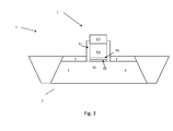
- a SiGe (or similar) capping layer 7 on top of the Ge layer (which can for instance constitute the germanium based channel layer and germanium based source and drain areas) is used, as illustrated in Fig. 3 , where the layer 7 is grown in a substantially facet-free mode.
- any formed facets of the SiGe layer can be covered by an extra spacer to avoid reaction of the metal on the facets.
- germano-silicide formation a portion of the capping layer remains that has a sufficiently high Si content to act as a sealing layer for the germanium during the selective etch.
- a relatively high silicon content is then preferred, as SiO 2 is not water soluble and thus forms a good passivation layer.
- a capping layer e.g., SiGe
- the metal e.g., Ni, NiPt
- This layer can be comprised primarily of Si, Ge, C, and Sn, but may also comprise dopant atoms, e.g., B, In, P, As, and Sb. If this layer is uniform in composition, the Ge concentration can be less than 70% and preferably less than 50%.
- the composition of the layer may also be nonuniform in depth, where the upper part which is adapted for reacting with the metal (e.g., Ni) may comprise a high Ge concentration (> 50%) whereas the lower, non-reacting part may comprise a high Si concentration (> 50%) to serve as the sealing layer.
- the metal e.g., Ni
- the upper part which is adapted for reacting with the metal may comprise a high Ge concentration (> 50%)
- the lower, non-reacting part may comprise a high Si concentration (> 50%) to serve as the sealing layer.
- the above mentioned capping layer is preferably such that it can grow selectively on Ge, but does not grow on dielectric materials for instance (e.g., Si02, SiN, SiON, C).
- dielectric materials e.g., Si02, SiN, SiON, C.
- the above mentioned capping layer may also be grown non-selectively, but must be subsequently removable from areas where it would be detrimental to device operation, using, for example, a chemical mechanical polish (CMP) operation.
- CMP chemical mechanical polish
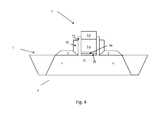
- a SiGe (or similar) capping layer 7 on top of the Ge layer can also be grown with facets, as illustrated in Fig. 4 .
- the facet on layer 7 can be covered with an extra spacer layer 56 to avoid reaction of the metal on the thin SiGe layer in the facet.
- the facet is covered by a premetal dielectric layer 80, in which openings 90 are provided.
- the opening 90 does not overlap on the facet of layer 7, i.e. the facets remain covered with the premetal dielectric layer 80.
- the premetal dielectric layer 80 covers the facets of layer 7.
- the formation of openings 90 in the premetal dielectric layer 80 and subsequent formation of the metal-germanium-silicide complex is done after the replacement gate process.
- the gate stack consists of the final dielectric layer 55, optional metal layer 54 and metal layer 58.
- the device depicted in Figure 9 results from further processing the device according to Figure 8 .
- a metal layer is provided on the capping layer 7 within the opening 90.
- An anneal step causes the partial consumption of the capping layer 7, and results in a remaining portion 72 of the original capping layer with on top a metal germano-silicide portion 71.
- the remaining unreacted portion of the metal layer can then be removed before contacts to the source and drain areas are formed through the premetal dielectric layer.
Landscapes
- Insulated Gate Type Field-Effect Transistor (AREA)
- Electrodes Of Semiconductors (AREA)
- Thin Film Transistor (AREA)
- Chemical & Material Sciences (AREA)
- Crystallography & Structural Chemistry (AREA)
Abstract
- providing a gate structure on the germanium comprising channel layer provided on a substrate, the gate structure being provided between a germanium based source area and a germanium based drain area at opposite sides of the germanium comprising channel layer;
- providing a capping layer on the germanium based source and the germanium based drain area, the capping layer comprising Si and Ge;
- depositing a metal layer on the capping layer;
- performing a temperature step, thereby transforming at least part of the capping layer into a metal germano-silicide which is not soluble in a predetermined etchant adapted for dissolving the metal;
- selectively removing non-consumed metal from the substrate by means of the predetermined etchant;
- providing a premetal dielectric layer.
Description
- The present invention relates generally to field-effect semiconductor devices, such as field-effect transistors (FETs).
- Several challenges still remain for large scale integration of field-effect semiconductor devices. As FET transistor gate lengths continue to scale down, the processes to define them are increasingly difficult to control in order to achieve the desired critical dimensions.
- Today, in the field of silicon based FET transistor devices, a self-aligned silicide process is usually included to reduce the resistance of the S/D regions and silicon gates. It typically comprises a preclean process, a metal deposition process and an anneal process to form a metal silicide alloy, followed by a wet selective etch to remove the non-reacted metal. During such a wet etch process, any exposed silicon surface (e.g. a silicon channel layer) automatically forms a thin passivating silicon oxide at its surface, protecting the underlying silicon from being affected.
- When manufacturing germanium based FET transistors, e.g. on a germanium substrate, a similar germanidation process has been developed in the state of the art. Here, void formation is a major issue when applying a germanidation process straight on a germanium surface. Such a germanidation process typically comprises a preclean process, a metal deposition process and an anneal process to form a metal germanide alloy, followed by a wet selective etch to remove the non-reacted metal. While the annealing temperature can be optimized to eliminate void formation caused by diffusion of Ge into the metal (e.g. Ni or NiPt) during the germanidation reaction itself (see for instance in
US 7,517,765 ), voids can still be formed during the selective etch for removing the non-reacted metal, which may be problematic. - The general problem is that germanium is susceptible to galvanic corrosion in aqueous solutions when in contact with a more noble metal. In the particular case of the germanide module, the germanium serves as an
anode 60 in a galvanic reaction while the more noble metal (e.g., NiGe, Ni, NiPtGe, NiPt) serves as the cathode 61 (illustrated inFig. 1 ). The void formation orpitting 62 can be quite severe as the area of the Ge exposed to the aqueous chemistry is small, resulting in high galvanic current densities and thus high local corrosion rates. As germanium oxide is water soluble, a thin passivating oxide layer cannot form. This is very different from the known silicidation process for silicon based FET transistors, for which SiO2 is not water soluble and is passivating in most aqueous solutions. - It is an aim of the present disclosure to provide an improved method for manufacturing a transistor device comprising a germanium based channel layer and germanium based source and drain areas by means of a germanidation process, which reduces or avoids void formation.
- This aim is achieved according to the disclosure with the method showing the technical characteristics of the first independent claim.
- According to a first embodiment of the present invention, a method for manufacturing a transistor device comprising a germanium or germanium based channel layer is disclosed, the method comprising:
- providing a gate structure on said germanium based channel layer provided on a substrate (for instance a germanium substrate, or a Si substrate with an epitaxial layer comprising Ge, or a SixGe1-x [0≤x ≤1] on Insulator substrate), the gate structure being provided between a germanium based source area and a germanium based drain area at opposite sides of the germanium based channel layer;
- providing a capping layer on the germanium based source area and germanium based drain area, the capping layer comprising silicon and germanium, e.g. comprising SiGe;
- depositing a metal layer on the capping layer;
- performing a temperature step, for instance an anneal step, thereby transforming at least part of the capping layer into a metal germano-silicide which is not soluble in a predetermined etchant adapted for dissolving the deposited metal layer;
- selectively removing a non-consumed metal layer from the substrate by means of the predetermined etchant;
- providing a premetal dielectric layer.
- It is an advantage that by providing the capping layer on the source and drain areas, before performing a germanidation process, void formation in the germanium based channel and/or source and drain areas can be reduced or avoided, as it prevents exposure of the germanium of the channel layer and source and drain areas and potentially other germanium based layers during the selective removing (e.g. etch) of the non-consumed metal layer. Preferably, an upper part of the capping layer reacts with the metal layer, while another, typically lower, unreacted part can function as an etch stop layer during the selective removing (e.g. etch) of the non-consumed metal layer.
- According to preferred embodiments, the method further comprises patterning the premetal dielectric layer such that open areas are created and filling the open areas with electrically conductive materials to connect source and drains to metallization lines. The premetal dielectric layer can for instance be a silicon oxide layer or a stack of silicon oxide / silicon nitride layer or a low-k dielectric.
- The channel layer can be a germanium based channel layer. It can for instance be a layer comprising more than 80%, or more than 90%, or more than 95%, or more than 99% germanium or can consist of 100% germanium.
- Each of the source and drain areas can be germanium based. They can for instance be a layer comprising more than 80%, or more than 90%, or more than 95%, or more than 99% germanium or can consist of 100% germanium.
- Providing a capping layer on at least the source and the drain areas, may also comprise providing the capping layer in the area between the gate structure and the source and drain areas respectively.
- Providing a temperature step may comprise providing a temperature between 150°C and 450°C. More preferably it may be a temperature between 200°C and 400°C. Even more preferably, it may be between 250 °C and 400 °C. Even more preferably, it may be a temperature between 250 °C and 350°C.
- According to preferred embodiments, the method comprises performing
- depositing the metal layer on the capping layer;
- performing the temperature step, thereby transforming at least part of the capping layer into a metal germano-silicide;
- selectively removing the non-consumed metal or metal layer from the substrate;
- This provides the advantage that the distance between the metal germano-silicide and the channel can be minimized. The distance can be mainly or completely determined by the spacer width.
- According to alternative preferred embodiments, the method comprises performing
- depositing the metal layer on the capping layer;
- performing the temperature step, thereby transforming at least part of the capping layer into a metal germano-silicide;
- selectively removing the non-consumed metal from the substrate;
- Postponing the formation of the metal germano-silicide until later in the process flow provides the advantage that other processing modules can be performed at process conditions, for instance temperatures, that the metal germano-silicide could not withstand. Such a process can be for instance a replacement metal gate process.
- According to preferred embodiments, the method further comprises replacing the gate structure by a final gate structure.
- According to preferred embodiments, replacing the gate structure by a final gate structure is performed after depositing the premetal dielectric layer, and for instance before patterning the premetal dielectric layer to expose the capping layer.
- According to preferred embodiments, the gate structure comprises one or more dielectric layers and a conductive electrode comprising one or more metal layers and/or a doped polycrystalline silicon layer. The gate structure is laterally limited by spacer structures, while the gate abuts on the germanium-comprising channel layer. The spacer structures may for instance comprise or consist of silicon nitride, a silicon oxide or a combination of both.
- According to preferred embodiments, the metal layer comprises or consists of Ni or Pt or both Ni and Pt, for instance a combination of Ni and Pt, or comprises of consists of Pd or Cu or both Pd and Cu, for instance a combination of Pd and Cu.
- Possible etchants corresponding therewith can be for instance hot HCl.
- According to preferred embodiments, providing the capping layer, e.g. SiGe layer, comprises epitaxially growing on the germanium based source and drain areas.
- According to preferred embodiments, the method comprises growing the capping layer, e.g. SiGe layer, in a substantially facet-free mode. As described further below, alternatively, the method may comprise covering the formed facets of the SiGe layer by an extra spacer to avoid reaction of the metal on the facets.
- According to preferred embodiments, the deposited metal layer is provided such that, for instance with a predetermined thickness and/or at predetermined locations, after the germanidation process (comprising depositing the metal layer on the capping layer and performing the temperature step), transforming at least part of the capping layer into a metal germano-silicide, a non-consumed (or unreacted or untransformed) portion of the capping layer remains covering the underlying germanium (preferably germanium based source and drain areas, but other, non-channel, germanium areas on the substrate may also be covered/protected), and thus protecting the underlying germanium from galvanic corrosion during the selective removing of the non-consumed or non-reacted metal layer from the substrate.
- According to preferred embodiments, the deposited metal layer has a predetermined thickness (for instance a thickness smaller than) with respect to the thickness of the capping layer comprising SiGe. In typical cases this would imply that not all of the capping layer would be consumed by interacting with the metal layer, such that a layer or portion of unreacted SiGe (or silicon, in case of a particular embodiment with a graded SiGe capping layer or bilayer having an 100% silicon bottom layer) remains covering and thus protecting the underlying germanium from galvanic corrosion. Preferably, the layer or portion of unreacted SiGe or Si of the capping layer has a thickness of at least 1 nm.
- For instance, a 1 nm thick layer of Ni would consume an approximately 2 nm thick layer of SixGe1-x (x in between 0 and 1), to form low resistance NiSixGe1-x phase. In order to have an unreacted or untransformed portion of the capping layer remaining, covering the underlying germanium, in this case the capping layer preferably has a thickness larger than 2 nm, e.g. 3 nm.
- According to preferred embodiments, the capping layer is adapted for preventing any exposure of the germanium based channel layer and source and drain areas to the predetermined etchant.
- According to preferred embodiments, the capping layer comprises Si and Ge, for instance SiGe, and comprises between 20 and 100% silicon. It is an advantage that a capping layer comprising enough silicon can suppress the germanium diffusion into the metal (e.g. Ni, NiPt) during the germanosilicide formation, and thereby also further addresses the problem of void formation during the anneal.
- The capping layer can have a uniform composition, and preferably comprises a germanium concentration below 70%, even more preferably below 50%. The capping layer may also comprise a non-uniform composition with depth such that the lower portion of the cap has a higher silicon concentration than the upper portion. For instance, the capping layer may comprise or consist of a bilayer, and may comprise a first sub-layer, a bottom layer, comprising a germanium concentration below 50%. The first sub-layer may comprise a silicon concentration higher than 50%. The capping layer can comprise a second sub-layer, a top layer, with a higher Germanium concentration, for instance above 50%, or above 70%. The first (bottom) sub-layer can be adapted to act as an etch-stop layer or sealing layer for, while the second (top) sub-layer may be adapted for optimally reacting with the metal layer. The capping layer can also be a graded layer with an increasing amount of germanium as the deposition thickness is increased. A bottom layer or lower portion of the graded capping layer can correspond to the first sub-layer as described for the bilayer embodiments. A top layer or upper portion of the graded capping layer can correspond to the second sub-layer as described for the bilayer embodiments. An intermediate graded portion may be provided in between such a top and bottom layers of the graded capping layer.
- The capping layer may further comprise C, Sn. The capping layer may further comprise, for instance, dopants such as B, In, P, As, or Sb.
- The capping layer can for instance have a thickness of at least 5 nm. It can have a thickness within the range of 5 nm to 30 nm.
- According to preferred embodiments, the method further comprises forming a spacer after growing the capping layer, e.g. SiGe layer, to cover any thin SiGe areas which may be present due to faceted SiGe growth, before depositing of the metal or metal layer. A thin area can be an area which would completely be consumed in the thickness direction, i.e. from the front surface of the capping layer up until the germanium based channel layer or source and drain areas, after depositing a predetermined metal layer on the capping layer and performing the temperature step. This would result in the fact that no unreacted portion of the capping layer is left in the thin area on the germanium based channel layer and/or source/drain areas, to protect the germanium based channel layer or source/drain areas.
- This spacer may be performed by processes known to the person skilled in the art.
- The spacer can comprise or can consist of a dielectric stack, e.g. silicon oxide or/and silicon nitride or any other low-k material that does not react with the metal used for the metal-silicon-germanium alloy.
- According to preferred embodiments, the (patterned) premetal dielectric layer serves to prevent any exposure of the germanium based channel layer and germanium based source and drain areas to the predetermined etchant. This can be achieved for instance by making a hole in the premetal dielectric in which the capping layer is opened up for reaction with the subsequently deposited metal, while the premetal dielectric is left covering any thin SiGe capping areas that may be present due to faceted SiGe growth. According to preferred embodiments, the method comprises performing a second temperature step (a 2nd anneal) after the selective etch (the removing of the non-consumed metal layer from the substrate) in order to reduce the resistance and/or improve the device properties of the metal germano-silicide.
- According to a second aspect of the present disclosure, a microelectronic device, for instance a transistor device or a device related to a transistor device as for instance an intermediate device while manufacturing a transistor device, is described comprising
- a germanium or germanium based channel layer on a substrate;
- a gate structure on the germanium based channel layer, the gate structure being positioned between a germanium based source and a germanium based drain area at opposite sides of the germanium based channel layer;
- a partially transformed capping layer on the source and/or drain area respectively only a portion of which comprises a metal germano-silicide.
- The portion which comprises a metal germano-silicide can be an upper portion or upper sublayer of the partially transformed capping layer. The partially transformed capping layer can further comprise silicon and/or germanium, for instance silicon germanium, preferably at its lower portion. The lower portion can be a lower sublayer.
- It will be appreciated by the skilled person that features and advantages described for the first aspect of the present invention are also applicable, mutatis mutandis, to the second aspect of the present invention and vice versa and are thereby also considered to be disclosed.
- The disclosure will be further elucidated by means of the following description and the appended figures.
-
Fig. 1 illustrates the anodizing process occurring in the state of the art germanidation process. -
Fig. 2 illustrates a state of the art germanium based FET transistor device produced by methods according to the state of the art, comprising voids in the germanium based source/drain areas. -
Fig. 3 illustrates a first embodiment according to the present disclosure. -
Fig. 4 illustrates a second embodiment according to the present disclosure, for instance based on the first embodiment. -
Fig. 5 illustrates a third embodiment according to the present disclosure, for instance based on the first embodiment. -
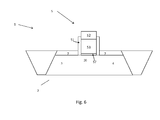
Fig. 6 illustrates fourth embodiment according to the present disclosure. -
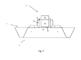
Fig. 7 illustrates a fifth embodiment according to the present disclosure. -
Fig. 8 illustrates a sixth embodiment according to the present disclosure. -
Fig. 9 illustrates an embodiment based on a further processing of the embodiment according toFig. 8 . - The present disclosure will be described with respect to particular embodiments and with reference to certain drawings but the disclosure is not limited thereto but only by the claims. The drawings described are only schematic and are non-limiting. In the drawings, the size of some of the elements may be exaggerated and not drawn on scale for illustrative purposes. The dimensions and the relative dimensions do not necessarily correspond to actual reductions to practice of the disclosure.
- Furthermore, the terms first, second, third and the like in the description and in the claims, are used for distinguishing between similar elements and not necessarily for describing a sequential or chronological order. The terms are interchangeable under appropriate circumstances and the embodiments of the disclosure can operate in other sequences than described or illustrated herein.
- Moreover, the terms top, bottom, over, under and the like in the description and the claims are used for descriptive purposes and not necessarily for describing relative positions. The terms so used are interchangeable under appropriate circumstances and the embodiments of the disclosure described herein can operate in other orientations than described or illustrated herein.
- Furthermore, the various embodiments, although referred to as "preferred" are to be construed as exemplary manners in which the disclosure may be implemented rather than as limiting the scope of the disclosure.
- The term "comprising", used in the claims, should not be interpreted as being restricted to the elements or steps listed thereafter; it does not exclude other elements or steps. It needs to be interpreted as specifying the presence of the stated features, integers, steps or components as referred to, but does not preclude the presence or addition of one or more other features, integers, steps or components, or groups thereof. Thus, the scope of the expression "a device comprising A and B" should not be limited to devices consisting only of components A and B, rather with respect to the present disclosure, the only enumerated components of the device are A and B, and further the claim should be interpreted as including equivalents of those components.
Figure 1 illustrates the fact that germanium is susceptible to galvanic corrosion in aqueous solutions when in contact with a more noble metal. In the particular case of the germanide module, the germanium serves as ananode 60 in a galvanic reaction while the more noble metal (e.g., NiGe, Ni, NiPt) serves as the cathode 61 (illustrated inFig. 1 ). The "more noble" metal is considered to be the metal with the higher standard electrode potential. -
Fig. 2 illustrates a typical germanium based FET transistor device. On or in a substrate, e.g. a germanium substrate, 2 aFET transistor device 1 is provided. Thesubstrate 2 comprises a channel layer orregion 20, which connects asource region 3 with adrain region 4. On top of the channel region 20 agate structure 5 is provided, in between the source region and the drain region. Thegate structure 5 comprises a dielectric layer orlayer stack 55, ametal layer 54, apolycrystalline silicon layer 53, and another dielectric layer 52 (for instance a silicon oxide layer). Laterally the stack is confined by a spacer structure orspacer 51, for instance a silicon nitride spacer. - According to prior art manufacturing methods, voids 6 are created and visible in the source and
drain areas - It is a general advantage of embodiments of the present disclosure that exposure of germanium which is in contact with a more noble metal during wet (aqueous) processes can be avoided, in order to suppress pitting in the germanium.
- According to preferred embodiments of the present disclosure, a SiGe (or similar)
capping layer 7 on top of the Ge layer (which can for instance constitute the germanium based channel layer and germanium based source and drain areas) is used, as illustrated inFig. 3 , where thelayer 7 is grown in a substantially facet-free mode. Alternatively, any formed facets of the SiGe layer can be covered by an extra spacer to avoid reaction of the metal on the facets. - After germano-silicide formation a portion of the capping layer remains that has a sufficiently high Si content to act as a sealing layer for the germanium during the selective etch. A relatively high silicon content is then preferred, as SiO2 is not water soluble and thus forms a good passivation layer.
- The growth of a capping layer (e.g., SiGe) before the metal deposition prevents germanium exposure to the aqueous solution during the selective etch where an excess of metal is removed. At least part of this capping layer reacts with the metal (e.g., Ni, NiPt) during the germanidation reaction and the unreacted part can serve as a stopping (sealing) layer to prevent exposure of the germanium to the wet etchant during the selective etch. This layer can be comprised primarily of Si, Ge, C, and Sn, but may also comprise dopant atoms, e.g., B, In, P, As, and Sb. If this layer is uniform in composition, the Ge concentration can be less than 70% and preferably less than 50%. According to certain embodiments, the composition of the layer may also be nonuniform in depth, where the upper part which is adapted for reacting with the metal (e.g., Ni) may comprise a high Ge concentration (> 50%) whereas the lower, non-reacting part may comprise a high Si concentration (> 50%) to serve as the sealing layer.
- The above mentioned capping layer is preferably such that it can grow selectively on Ge, but does not grow on dielectric materials for instance (e.g., Si02, SiN, SiON, C).The above mentioned capping layer may also be grown non-selectively, but must be subsequently removable from areas where it would be detrimental to device operation, using, for example, a chemical mechanical polish (CMP) operation.
- According to preferred embodiments of the present disclosure, a SiGe (or similar)
capping layer 7 on top of the Ge layer can also be grown with facets, as illustrated inFig. 4 . In this case, the facet onlayer 7 can be covered with anextra spacer layer 56 to avoid reaction of the metal on the thin SiGe layer in the facet. - In
figure 5 the facet is covered by apremetal dielectric layer 80, in whichopenings 90 are provided. Theopening 90 does not overlap on the facet oflayer 7, i.e. the facets remain covered with thepremetal dielectric layer 80. As such, thepremetal dielectric layer 80 covers the facets oflayer 7. - The embodiments depicted in
Figures 6 to 8 are equivalent to those offigures 3 to 5 respectively for the integration approach where a replacement gate process is used. In case the formation of the metal-germanium-silicide complex is done prior to the gate removal process, the gate stack at the moment of the germano-silicidation consists out of adummy dielectric layer 57 and dummypolysilicon gate layer 53. - In
figure 8 , the formation ofopenings 90 in thepremetal dielectric layer 80 and subsequent formation of the metal-germanium-silicide complex is done after the replacement gate process. In this case, the gate stack consists of thefinal dielectric layer 55,optional metal layer 54 andmetal layer 58. - The device depicted in
Figure 9 results from further processing the device according toFigure 8 . A metal layer is provided on thecapping layer 7 within theopening 90. An anneal step causes the partial consumption of thecapping layer 7, and results in a remainingportion 72 of the original capping layer with on top a metal germano-silicide portion 71. The remaining unreacted portion of the metal layer can then be removed before contacts to the source and drain areas are formed through the premetal dielectric layer.
Claims (15)
- A method for manufacturing a transistor device comprising a germanium based channel layer, said method comprising :- providing a gate structure on said germanium based channel layer provided on a substrate, said gate structure being provided between a germanium based source area and a germanium based drain area at opposite sides of said germanium based channel layer;- providing a capping layer on said germanium based source and said germanium based drain area, said capping layer comprising Si and Ge;- depositing a metal layer on said capping layer;- performing a temperature step, thereby transforming at least part of said capping layer into a metal germano-silicide which is not soluble in a predetermined etchant adapted for dissolving said metal;- selectively removing non-consumed metal from said substrate by means of said predetermined etchant;- providing a premetal dielectric layer.
- A method according to claim 1, comprising performing- depositing said metal layer on said capping layer;- performing said temperature step, thereby transforming at least part of said capping layer into a metal germano-silicide;- selectively removing said non-consumed metal from said substrate;
before depositing said premetal dielectric layer. - A method according to claim 1, comprising performing- depositing said metal layer on said capping layer;- performing said temperature step, thereby transforming at least part of said capping layer into a metal germano-silicide;- selectively removing said non-consumed metal from said
substrate;
after depositing and patterning openings in said premetal dielectric layer. - A method according to any of the previous claims, further comprising replacing said gate structure by a final gate structure.
- A method according to claim 4, wherein replacing said gate structure by a final gate structure is performed after depositing said premetal dielectric layer.
- A method according to any of the previous claims, wherein said metal layer comprises Ni or Pt or a combination of Ni and Pt, or Pd or Cu, or a combination of Pd and Cu.
- Method according to any of the previous claims, wherein providing said capping layer comprises epitaxially growing said capping layer on said germanium based source and drain areas.
- Method according to any of the previous claims, wherein the deposited metal layer is provided such that, after depositing said metal layer on the capping layer and performing said temperature step, thereby transforming at least part of the capping layer into a metal germano-silicide, an unreacted or untransformed portion of the capping layer remains covering the underlying germanium based channel layer.
- Method according to any of the previous claims, wherein said capping layer comprises SiGe and contains between 20 and 100% silicon.
- Method according to claim 9, comprising forming a spacer after growing said capping layer to cover any thin SiGe areas which may be present due to faceted SiGe growth, before depositing said metal layer on said capping layer.
- Method according to any of the previous claims 1 to 9, comprising growing said capping layer in a substantially facet-free mode.
- Method according to any of the previous claims, wherein said capping layer is adapted for preventing any exposure of the germanium based channel layer and germanium based source and drain areas to said predetermined etchant.
- Method according to any of the previous claims, wherein said capping layer has a thickness of at least 5 nm.
- Method according to the any of the previous claims, wherein said premetal dielectric serves to prevent any exposure of the germanium based channel layer and germanium based source and drain areas to said predetermined etchant.
- A microelectronic device comprising- a germanium based channel layer on a substrate;- a gate structure on said germanium based channel layer, said gate structure being positioned between a germanium based source area and a germanium drain area at opposite sides of said germanium based channel layer;a partially transformed capping layer on said source and/or drain area respectively, only a portion of which comprises a metal germano-silicide.
Priority Applications (5)
| Application Number | Priority Date | Filing Date | Title |
|---|---|---|---|
| EP12182800.8A EP2704199B1 (en) | 2012-09-03 | 2012-09-03 | Method of manufacturing a semiconductor device |
| US14/015,531 US8828826B2 (en) | 2012-09-03 | 2013-08-30 | Method for manufacturing a transistor device comprising a germanium based channel layer |
| JP2013180908A JP6376736B2 (en) | 2012-09-03 | 2013-09-02 | Semiconductor device and manufacturing method thereof |
| CN201310394909.5A CN103681353B (en) | 2012-09-03 | 2013-09-03 | Fabrication method and microelectronic device of transistor device with channel layer mainly containing germanium |
| TW102131620A TWI512843B (en) | 2012-09-03 | 2013-09-03 | Method for fabricating transistor device including channel layer based on germanium and microelectronic device |
Applications Claiming Priority (1)
| Application Number | Priority Date | Filing Date | Title |
|---|---|---|---|
| EP12182800.8A EP2704199B1 (en) | 2012-09-03 | 2012-09-03 | Method of manufacturing a semiconductor device |
Publications (2)
| Publication Number | Publication Date |
|---|---|
| EP2704199A1 true EP2704199A1 (en) | 2014-03-05 |
| EP2704199B1 EP2704199B1 (en) | 2020-01-01 |
Family
ID=46799120
Family Applications (1)
| Application Number | Title | Priority Date | Filing Date |
|---|---|---|---|
| EP12182800.8A Active EP2704199B1 (en) | 2012-09-03 | 2012-09-03 | Method of manufacturing a semiconductor device |
Country Status (5)
| Country | Link |
|---|---|
| US (1) | US8828826B2 (en) |
| EP (1) | EP2704199B1 (en) |
| JP (1) | JP6376736B2 (en) |
| CN (1) | CN103681353B (en) |
| TW (1) | TWI512843B (en) |
Families Citing this family (3)
| Publication number | Priority date | Publication date | Assignee | Title |
|---|---|---|---|---|
| EP2704199B1 (en) * | 2012-09-03 | 2020-01-01 | IMEC vzw | Method of manufacturing a semiconductor device |
| KR20190110845A (en) * | 2018-03-21 | 2019-10-01 | 삼성전자주식회사 | Semiconductor device |
| US11373870B2 (en) * | 2019-06-27 | 2022-06-28 | Taiwan Semiconductor Manufacturing Co., Ltd. | Method for manufacturing semiconductor device including performing thermal treatment on germanium layer |
Citations (6)
| Publication number | Priority date | Publication date | Assignee | Title |
|---|---|---|---|---|
| US20040217430A1 (en) * | 2003-05-01 | 2004-11-04 | Chu Jack Oon | High performance FET devices and methods therefor |
| US20050006637A1 (en) * | 2003-07-11 | 2005-01-13 | Toshihiko Iinuma | Semiconductor device and method of manufacturing the same |
| US20050250301A1 (en) * | 2004-05-04 | 2005-11-10 | International Business Machines Corporation | Self-aligned metal to form contacts to Ge containing substrates and structure formed thereby |
| US7517765B2 (en) | 2004-03-08 | 2009-04-14 | Interuniversitair Microelektronica Centrum (Imec) | Method for forming germanides and devices obtained thereof |
| US20090108308A1 (en) * | 2007-10-31 | 2009-04-30 | Jusung Engineering Co., Ltd | Transistor and method of fabricating the same |
| US20120168830A1 (en) * | 2011-01-05 | 2012-07-05 | Koji Usuda | Semiconductor device and method of manufacturing the same |
Family Cites Families (26)
| Publication number | Priority date | Publication date | Assignee | Title |
|---|---|---|---|---|
| JP3544833B2 (en) * | 1997-09-18 | 2004-07-21 | 株式会社東芝 | Semiconductor device and manufacturing method thereof |
| JP2005032962A (en) * | 2003-07-11 | 2005-02-03 | Toshiba Corp | Semiconductor device |
| US6949482B2 (en) | 2003-12-08 | 2005-09-27 | Intel Corporation | Method for improving transistor performance through reducing the salicide interface resistance |
| US20070272955A1 (en) | 2004-07-27 | 2007-11-29 | Agency For Science, Technology And Research | Reliable Contacts |
| JP4940682B2 (en) | 2005-09-09 | 2012-05-30 | 富士通セミコンダクター株式会社 | Field effect transistor and manufacturing method thereof |
| US7491643B2 (en) * | 2006-05-24 | 2009-02-17 | International Business Machines Corporation | Method and structure for reducing contact resistance between silicide contact and overlying metallization |
| KR100798814B1 (en) | 2006-09-20 | 2008-01-28 | 삼성전자주식회사 | Semiconductor device including field effect transistor and method for forming same |
| US20080119025A1 (en) * | 2006-11-21 | 2008-05-22 | O Sung Kwon | Method of making a strained semiconductor device |
| US7750338B2 (en) * | 2006-12-05 | 2010-07-06 | Taiwan Semiconductor Manufacturing Company, Ltd. | Dual-SiGe epitaxy for MOS devices |
| US8344447B2 (en) * | 2007-04-05 | 2013-01-01 | Taiwan Semiconductor Manufacturing Company, Ltd. | Silicon layer for stopping dislocation propagation |
| JP5653577B2 (en) * | 2007-08-31 | 2015-01-14 | アイメックImec | Improved method of germanide growth and device obtained thereby |
| US8299453B2 (en) * | 2009-03-03 | 2012-10-30 | International Business Machines Corporation | CMOS transistors with silicon germanium channel and dual embedded stressors |
| DE102009015748B4 (en) | 2009-03-31 | 2014-05-22 | Globalfoundries Dresden Module One Limited Liability Company & Co. Kg | Reducing the silicide resistance in SiGe-containing drain / source regions of transistors |
| JP5287539B2 (en) * | 2009-06-23 | 2013-09-11 | 富士通セミコンダクター株式会社 | Manufacturing method of semiconductor device |
| CN101635262B (en) | 2009-08-07 | 2012-05-30 | 北京大学 | Preparation method of germanium-base schottky transistor |
| US8129234B2 (en) * | 2009-09-09 | 2012-03-06 | International Business Machines Corporation | Method of forming bipolar transistor integrated with metal gate CMOS devices |
| JP2011071224A (en) * | 2009-09-24 | 2011-04-07 | Toshiba Corp | Semiconductor device and manufacturing method thereof |
| US20110147809A1 (en) * | 2009-12-22 | 2011-06-23 | Bin Yang | Forming a carbon containing layer to facilitate silicide stability in a silicon germanium material |
| US8278179B2 (en) * | 2010-03-09 | 2012-10-02 | Taiwan Semiconductor Manufacturing Co., Ltd. | LDD epitaxy for FinFETs |
| US8237197B2 (en) * | 2010-07-07 | 2012-08-07 | International Business Machines Corporation | Asymmetric channel MOSFET |
| US8358012B2 (en) * | 2010-08-03 | 2013-01-22 | International Business Machines Corporation | Metal semiconductor alloy structure for low contact resistance |
| US8354694B2 (en) * | 2010-08-13 | 2013-01-15 | International Business Machines Corporation | CMOS transistors with stressed high mobility channels |
| US8901537B2 (en) * | 2010-12-21 | 2014-12-02 | Intel Corporation | Transistors with high concentration of boron doped germanium |
| US8994097B2 (en) * | 2012-03-08 | 2015-03-31 | Taiwan Semiconductor Manufacturing Company, Ltd. | MOS devices having non-uniform stressor doping |
| US20130256757A1 (en) * | 2012-03-29 | 2013-10-03 | International Business Machines Corporation | Soi lateral bipolar junction transistor having a wide band gap emitter contact |
| EP2704199B1 (en) * | 2012-09-03 | 2020-01-01 | IMEC vzw | Method of manufacturing a semiconductor device |
-
2012
- 2012-09-03 EP EP12182800.8A patent/EP2704199B1/en active Active
-
2013
- 2013-08-30 US US14/015,531 patent/US8828826B2/en active Active
- 2013-09-02 JP JP2013180908A patent/JP6376736B2/en active Active
- 2013-09-03 TW TW102131620A patent/TWI512843B/en active
- 2013-09-03 CN CN201310394909.5A patent/CN103681353B/en active Active
Patent Citations (6)
| Publication number | Priority date | Publication date | Assignee | Title |
|---|---|---|---|---|
| US20040217430A1 (en) * | 2003-05-01 | 2004-11-04 | Chu Jack Oon | High performance FET devices and methods therefor |
| US20050006637A1 (en) * | 2003-07-11 | 2005-01-13 | Toshihiko Iinuma | Semiconductor device and method of manufacturing the same |
| US7517765B2 (en) | 2004-03-08 | 2009-04-14 | Interuniversitair Microelektronica Centrum (Imec) | Method for forming germanides and devices obtained thereof |
| US20050250301A1 (en) * | 2004-05-04 | 2005-11-10 | International Business Machines Corporation | Self-aligned metal to form contacts to Ge containing substrates and structure formed thereby |
| US20090108308A1 (en) * | 2007-10-31 | 2009-04-30 | Jusung Engineering Co., Ltd | Transistor and method of fabricating the same |
| US20120168830A1 (en) * | 2011-01-05 | 2012-07-05 | Koji Usuda | Semiconductor device and method of manufacturing the same |
Non-Patent Citations (1)
| Title |
|---|
| GUANG-LI LUO ET AL: "A comprehensive study of Ge1- xSix on Ge for the Ge nMOSFETs with tensile stress, shallow junctions and reduced leakage", ELECTRON DEVICES MEETING (IEDM), 2009 IEEE INTERNATIONAL, IEEE, PISCATAWAY, NJ, USA, 7 December 2009 (2009-12-07), pages 1 - 4, XP031644428, ISBN: 978-1-4244-5639-0 * |
Also Published As
| Publication number | Publication date |
|---|---|
| US20140061735A1 (en) | 2014-03-06 |
| CN103681353B (en) | 2017-05-10 |
| JP2014049768A (en) | 2014-03-17 |
| TW201411735A (en) | 2014-03-16 |
| EP2704199B1 (en) | 2020-01-01 |
| JP6376736B2 (en) | 2018-08-22 |
| US8828826B2 (en) | 2014-09-09 |
| TWI512843B (en) | 2015-12-11 |
| CN103681353A (en) | 2014-03-26 |
Similar Documents
| Publication | Publication Date | Title |
|---|---|---|
| US7396767B2 (en) | Semiconductor structure including silicide regions and method of making same | |
| US10115597B2 (en) | Self-aligned dual-metal silicide and germanide formation | |
| CN101981670B (en) | Selective Formation of Dielectric Etch Stop Layer | |
| KR102432086B1 (en) | Self-aligned contacts | |
| US20010014533A1 (en) | Method of fabricating salicide | |
| KR101510029B1 (en) | Transistors with high concentration of boron doped germanium | |
| US20050272235A1 (en) | Method of forming silicided gate structure | |
| US12166078B2 (en) | Contact structure for semiconductor device and method | |
| CN108257916A (en) | Semiconductor structure and forming method thereof | |
| CN103390549B (en) | Semiconductor device manufacturing method | |
| US20070026593A1 (en) | Diffusion barrier for nickel silicides in a semiconductor fabrication process | |
| US8828826B2 (en) | Method for manufacturing a transistor device comprising a germanium based channel layer | |
| KR102434065B1 (en) | Semiconductor device and manufacturing method thereof | |
| US6207563B1 (en) | Low-leakage CoSi2-processing by high temperature thermal processing | |
| US11742406B2 (en) | Semiconductor device and fabrication method thereof | |
| US8536053B2 (en) | Method for restricting lateral encroachment of metal silicide into channel region | |
| US7329582B1 (en) | Methods for fabricating a semiconductor device, which include selectively depositing an electrically conductive material | |
| KR20070015004A (en) | How to Form a Silicided Gate | |
| US7109116B1 (en) | Method for reducing dendrite formation in nickel silicon salicide processes | |
| US7064067B1 (en) | Reduction of lateral silicide growth in integrated circuit technology | |
| US12283523B2 (en) | Semiconductor device and fabrication method thereof | |
| US7151020B1 (en) | Conversion of transition metal to silicide through back end processing in integrated circuit technology | |
| KR100230388B1 (en) | Method for forming transistor of semiconductor device |
Legal Events
| Date | Code | Title | Description |
|---|---|---|---|
| AK | Designated contracting states |
Kind code of ref document: A1 Designated state(s): AL AT BE BG CH CY CZ DE DK EE ES FI FR GB GR HR HU IE IS IT LI LT LU LV MC MK MT NL NO PL PT RO RS SE SI SK SM TR |
|
| AX | Request for extension of the european patent |
Extension state: BA ME |
|
| PUAI | Public reference made under article 153(3) epc to a published international application that has entered the european phase |
Free format text: ORIGINAL CODE: 0009012 |
|
| 17P | Request for examination filed |
Effective date: 20140901 |
|
| RBV | Designated contracting states (corrected) |
Designated state(s): AL AT BE BG CH CY CZ DE DK EE ES FI FR GB GR HR HU IE IS IT LI LT LU LV MC MK MT NL NO PL PT RO RS SE SI SK SM TR |
|
| STAA | Information on the status of an ep patent application or granted ep patent |
Free format text: STATUS: EXAMINATION IS IN PROGRESS |
|
| 17Q | First examination report despatched |
Effective date: 20170630 |
|
| RAP1 | Party data changed (applicant data changed or rights of an application transferred) |
Owner name: TAIWAN SEMICONDUCTOR MANUFACTURING COMPANY, LIMITE Owner name: IMEC VZW |
|
| GRAP | Despatch of communication of intention to grant a patent |
Free format text: ORIGINAL CODE: EPIDOSNIGR1 |
|
| STAA | Information on the status of an ep patent application or granted ep patent |
Free format text: STATUS: GRANT OF PATENT IS INTENDED |
|
| INTG | Intention to grant announced |
Effective date: 20191018 |
|
| GRAS | Grant fee paid |
Free format text: ORIGINAL CODE: EPIDOSNIGR3 |
|
| GRAA | (expected) grant |
Free format text: ORIGINAL CODE: 0009210 |
|
| STAA | Information on the status of an ep patent application or granted ep patent |
Free format text: STATUS: THE PATENT HAS BEEN GRANTED |
|
| AK | Designated contracting states |
Kind code of ref document: B1 Designated state(s): AL AT BE BG CH CY CZ DE DK EE ES FI FR GB GR HR HU IE IS IT LI LT LU LV MC MK MT NL NO PL PT RO RS SE SI SK SM TR |
|
| REG | Reference to a national code |
Ref country code: GB Ref legal event code: FG4D |
|
| REG | Reference to a national code |
Ref country code: CH Ref legal event code: EP Ref country code: AT Ref legal event code: REF Ref document number: 1220877 Country of ref document: AT Kind code of ref document: T Effective date: 20200115 |
|
| REG | Reference to a national code |
Ref country code: IE Ref legal event code: FG4D |
|
| REG | Reference to a national code |
Ref country code: DE Ref legal event code: R096 Ref document number: 602012066850 Country of ref document: DE |
|
| REG | Reference to a national code |
Ref country code: NL Ref legal event code: MP Effective date: 20200101 |
|
| REG | Reference to a national code |
Ref country code: LT Ref legal event code: MG4D |
|
| PG25 | Lapsed in a contracting state [announced via postgrant information from national office to epo] |
Ref country code: RS Free format text: LAPSE BECAUSE OF FAILURE TO SUBMIT A TRANSLATION OF THE DESCRIPTION OR TO PAY THE FEE WITHIN THE PRESCRIBED TIME-LIMIT Effective date: 20200101 Ref country code: LT Free format text: LAPSE BECAUSE OF FAILURE TO SUBMIT A TRANSLATION OF THE DESCRIPTION OR TO PAY THE FEE WITHIN THE PRESCRIBED TIME-LIMIT Effective date: 20200101 Ref country code: PT Free format text: LAPSE BECAUSE OF FAILURE TO SUBMIT A TRANSLATION OF THE DESCRIPTION OR TO PAY THE FEE WITHIN THE PRESCRIBED TIME-LIMIT Effective date: 20200527 Ref country code: CZ Free format text: LAPSE BECAUSE OF FAILURE TO SUBMIT A TRANSLATION OF THE DESCRIPTION OR TO PAY THE FEE WITHIN THE PRESCRIBED TIME-LIMIT Effective date: 20200101 Ref country code: NL Free format text: LAPSE BECAUSE OF FAILURE TO SUBMIT A TRANSLATION OF THE DESCRIPTION OR TO PAY THE FEE WITHIN THE PRESCRIBED TIME-LIMIT Effective date: 20200101 Ref country code: NO Free format text: LAPSE BECAUSE OF FAILURE TO SUBMIT A TRANSLATION OF THE DESCRIPTION OR TO PAY THE FEE WITHIN THE PRESCRIBED TIME-LIMIT Effective date: 20200401 Ref country code: FI Free format text: LAPSE BECAUSE OF FAILURE TO SUBMIT A TRANSLATION OF THE DESCRIPTION OR TO PAY THE FEE WITHIN THE PRESCRIBED TIME-LIMIT Effective date: 20200101 |
|
| PG25 | Lapsed in a contracting state [announced via postgrant information from national office to epo] |
Ref country code: SE Free format text: LAPSE BECAUSE OF FAILURE TO SUBMIT A TRANSLATION OF THE DESCRIPTION OR TO PAY THE FEE WITHIN THE PRESCRIBED TIME-LIMIT Effective date: 20200101 Ref country code: LV Free format text: LAPSE BECAUSE OF FAILURE TO SUBMIT A TRANSLATION OF THE DESCRIPTION OR TO PAY THE FEE WITHIN THE PRESCRIBED TIME-LIMIT Effective date: 20200101 Ref country code: HR Free format text: LAPSE BECAUSE OF FAILURE TO SUBMIT A TRANSLATION OF THE DESCRIPTION OR TO PAY THE FEE WITHIN THE PRESCRIBED TIME-LIMIT Effective date: 20200101 Ref country code: BG Free format text: LAPSE BECAUSE OF FAILURE TO SUBMIT A TRANSLATION OF THE DESCRIPTION OR TO PAY THE FEE WITHIN THE PRESCRIBED TIME-LIMIT Effective date: 20200401 Ref country code: GR Free format text: LAPSE BECAUSE OF FAILURE TO SUBMIT A TRANSLATION OF THE DESCRIPTION OR TO PAY THE FEE WITHIN THE PRESCRIBED TIME-LIMIT Effective date: 20200402 Ref country code: IS Free format text: LAPSE BECAUSE OF FAILURE TO SUBMIT A TRANSLATION OF THE DESCRIPTION OR TO PAY THE FEE WITHIN THE PRESCRIBED TIME-LIMIT Effective date: 20200501 |
|
| REG | Reference to a national code |
Ref country code: DE Ref legal event code: R097 Ref document number: 602012066850 Country of ref document: DE |
|
| PG25 | Lapsed in a contracting state [announced via postgrant information from national office to epo] |
Ref country code: SK Free format text: LAPSE BECAUSE OF FAILURE TO SUBMIT A TRANSLATION OF THE DESCRIPTION OR TO PAY THE FEE WITHIN THE PRESCRIBED TIME-LIMIT Effective date: 20200101 Ref country code: RO Free format text: LAPSE BECAUSE OF FAILURE TO SUBMIT A TRANSLATION OF THE DESCRIPTION OR TO PAY THE FEE WITHIN THE PRESCRIBED TIME-LIMIT Effective date: 20200101 Ref country code: DK Free format text: LAPSE BECAUSE OF FAILURE TO SUBMIT A TRANSLATION OF THE DESCRIPTION OR TO PAY THE FEE WITHIN THE PRESCRIBED TIME-LIMIT Effective date: 20200101 Ref country code: SM Free format text: LAPSE BECAUSE OF FAILURE TO SUBMIT A TRANSLATION OF THE DESCRIPTION OR TO PAY THE FEE WITHIN THE PRESCRIBED TIME-LIMIT Effective date: 20200101 Ref country code: EE Free format text: LAPSE BECAUSE OF FAILURE TO SUBMIT A TRANSLATION OF THE DESCRIPTION OR TO PAY THE FEE WITHIN THE PRESCRIBED TIME-LIMIT Effective date: 20200101 Ref country code: ES Free format text: LAPSE BECAUSE OF FAILURE TO SUBMIT A TRANSLATION OF THE DESCRIPTION OR TO PAY THE FEE WITHIN THE PRESCRIBED TIME-LIMIT Effective date: 20200101 |
|
| PLBE | No opposition filed within time limit |
Free format text: ORIGINAL CODE: 0009261 |
|
| STAA | Information on the status of an ep patent application or granted ep patent |
Free format text: STATUS: NO OPPOSITION FILED WITHIN TIME LIMIT |
|
| REG | Reference to a national code |
Ref country code: AT Ref legal event code: MK05 Ref document number: 1220877 Country of ref document: AT Kind code of ref document: T Effective date: 20200101 |
|
| 26N | No opposition filed |
Effective date: 20201002 |
|
| PG25 | Lapsed in a contracting state [announced via postgrant information from national office to epo] |
Ref country code: AT Free format text: LAPSE BECAUSE OF FAILURE TO SUBMIT A TRANSLATION OF THE DESCRIPTION OR TO PAY THE FEE WITHIN THE PRESCRIBED TIME-LIMIT Effective date: 20200101 Ref country code: IT Free format text: LAPSE BECAUSE OF FAILURE TO SUBMIT A TRANSLATION OF THE DESCRIPTION OR TO PAY THE FEE WITHIN THE PRESCRIBED TIME-LIMIT Effective date: 20200101 |
|
| PG25 | Lapsed in a contracting state [announced via postgrant information from national office to epo] |
Ref country code: PL Free format text: LAPSE BECAUSE OF FAILURE TO SUBMIT A TRANSLATION OF THE DESCRIPTION OR TO PAY THE FEE WITHIN THE PRESCRIBED TIME-LIMIT Effective date: 20200101 Ref country code: SI Free format text: LAPSE BECAUSE OF FAILURE TO SUBMIT A TRANSLATION OF THE DESCRIPTION OR TO PAY THE FEE WITHIN THE PRESCRIBED TIME-LIMIT Effective date: 20200101 |
|
| PG25 | Lapsed in a contracting state [announced via postgrant information from national office to epo] |
Ref country code: MC Free format text: LAPSE BECAUSE OF FAILURE TO SUBMIT A TRANSLATION OF THE DESCRIPTION OR TO PAY THE FEE WITHIN THE PRESCRIBED TIME-LIMIT Effective date: 20200101 |
|
| REG | Reference to a national code |
Ref country code: CH Ref legal event code: PL |
|
| GBPC | Gb: european patent ceased through non-payment of renewal fee |
Effective date: 20200903 |
|
| REG | Reference to a national code |
Ref country code: BE Ref legal event code: MM Effective date: 20200930 |
|
| PG25 | Lapsed in a contracting state [announced via postgrant information from national office to epo] |
Ref country code: LU Free format text: LAPSE BECAUSE OF NON-PAYMENT OF DUE FEES Effective date: 20200903 |
|
| PG25 | Lapsed in a contracting state [announced via postgrant information from national office to epo] |
Ref country code: LI Free format text: LAPSE BECAUSE OF NON-PAYMENT OF DUE FEES Effective date: 20200930 Ref country code: IE Free format text: LAPSE BECAUSE OF NON-PAYMENT OF DUE FEES Effective date: 20200903 Ref country code: GB Free format text: LAPSE BECAUSE OF NON-PAYMENT OF DUE FEES Effective date: 20200903 Ref country code: BE Free format text: LAPSE BECAUSE OF NON-PAYMENT OF DUE FEES Effective date: 20200930 Ref country code: CH Free format text: LAPSE BECAUSE OF NON-PAYMENT OF DUE FEES Effective date: 20200930 |
|
| PG25 | Lapsed in a contracting state [announced via postgrant information from national office to epo] |
Ref country code: TR Free format text: LAPSE BECAUSE OF FAILURE TO SUBMIT A TRANSLATION OF THE DESCRIPTION OR TO PAY THE FEE WITHIN THE PRESCRIBED TIME-LIMIT Effective date: 20200101 Ref country code: MT Free format text: LAPSE BECAUSE OF FAILURE TO SUBMIT A TRANSLATION OF THE DESCRIPTION OR TO PAY THE FEE WITHIN THE PRESCRIBED TIME-LIMIT Effective date: 20200101 Ref country code: CY Free format text: LAPSE BECAUSE OF FAILURE TO SUBMIT A TRANSLATION OF THE DESCRIPTION OR TO PAY THE FEE WITHIN THE PRESCRIBED TIME-LIMIT Effective date: 20200101 |
|
| PG25 | Lapsed in a contracting state [announced via postgrant information from national office to epo] |
Ref country code: MK Free format text: LAPSE BECAUSE OF FAILURE TO SUBMIT A TRANSLATION OF THE DESCRIPTION OR TO PAY THE FEE WITHIN THE PRESCRIBED TIME-LIMIT Effective date: 20200101 Ref country code: AL Free format text: LAPSE BECAUSE OF FAILURE TO SUBMIT A TRANSLATION OF THE DESCRIPTION OR TO PAY THE FEE WITHIN THE PRESCRIBED TIME-LIMIT Effective date: 20200101 |
|
| P01 | Opt-out of the competence of the unified patent court (upc) registered |
Effective date: 20230513 |
|
| REG | Reference to a national code |
Ref country code: DE Ref legal event code: R079 Ref document number: 602012066850 Country of ref document: DE Free format text: PREVIOUS MAIN CLASS: H01L0029165000 Ipc: H10D0062822000 |
|
| PGFP | Annual fee paid to national office [announced via postgrant information from national office to epo] |
Ref country code: DE Payment date: 20250820 Year of fee payment: 14 |
|
| PGFP | Annual fee paid to national office [announced via postgrant information from national office to epo] |
Ref country code: FR Payment date: 20250820 Year of fee payment: 14 |