EP2703964A1 - Touch-control screen and mobile communications device - Google Patents
Touch-control screen and mobile communications device Download PDFInfo
- Publication number
- EP2703964A1 EP2703964A1 EP13179396.0A EP13179396A EP2703964A1 EP 2703964 A1 EP2703964 A1 EP 2703964A1 EP 13179396 A EP13179396 A EP 13179396A EP 2703964 A1 EP2703964 A1 EP 2703964A1
- Authority
- EP
- European Patent Office
- Prior art keywords
- touch
- shield layer
- control screen
- liquid crystal
- crystal display
- Prior art date
- Legal status (The legal status is an assumption and is not a legal conclusion. Google has not performed a legal analysis and makes no representation as to the accuracy of the status listed.)
- Granted
Links
Images


Classifications
-
- G—PHYSICS
- G02—OPTICS
- G02F—OPTICAL DEVICES OR ARRANGEMENTS FOR THE CONTROL OF LIGHT BY MODIFICATION OF THE OPTICAL PROPERTIES OF THE MEDIA OF THE ELEMENTS INVOLVED THEREIN; NON-LINEAR OPTICS; FREQUENCY-CHANGING OF LIGHT; OPTICAL LOGIC ELEMENTS; OPTICAL ANALOGUE/DIGITAL CONVERTERS
- G02F1/00—Devices or arrangements for the control of the intensity, colour, phase, polarisation or direction of light arriving from an independent light source, e.g. switching, gating or modulating; Non-linear optics
- G02F1/01—Devices or arrangements for the control of the intensity, colour, phase, polarisation or direction of light arriving from an independent light source, e.g. switching, gating or modulating; Non-linear optics for the control of the intensity, phase, polarisation or colour
- G02F1/13—Devices or arrangements for the control of the intensity, colour, phase, polarisation or direction of light arriving from an independent light source, e.g. switching, gating or modulating; Non-linear optics for the control of the intensity, phase, polarisation or colour based on liquid crystals, e.g. single liquid crystal display cells
- G02F1/133—Constructional arrangements; Operation of liquid crystal cells; Circuit arrangements
- G02F1/1333—Constructional arrangements; Manufacturing methods
- G02F1/13338—Input devices, e.g. touch panels
-
- G—PHYSICS
- G06—COMPUTING OR CALCULATING; COUNTING
- G06F—ELECTRIC DIGITAL DATA PROCESSING
- G06F1/00—Details not covered by groups G06F3/00 - G06F13/00 and G06F21/00
- G06F1/16—Constructional details or arrangements
- G06F1/18—Packaging or power distribution
- G06F1/181—Enclosures
- G06F1/182—Enclosures with special features, e.g. for use in industrial environments; grounding or shielding against radio frequency interference [RFI] or electromagnetical interference [EMI]
-
- G—PHYSICS
- G06—COMPUTING OR CALCULATING; COUNTING
- G06F—ELECTRIC DIGITAL DATA PROCESSING
- G06F3/00—Input arrangements for transferring data to be processed into a form capable of being handled by the computer; Output arrangements for transferring data from processing unit to output unit, e.g. interface arrangements
- G06F3/01—Input arrangements or combined input and output arrangements for interaction between user and computer
- G06F3/03—Arrangements for converting the position or the displacement of a member into a coded form
- G06F3/041—Digitisers, e.g. for touch screens or touch pads, characterised by the transducing means
-
- G—PHYSICS
- G02—OPTICS
- G02F—OPTICAL DEVICES OR ARRANGEMENTS FOR THE CONTROL OF LIGHT BY MODIFICATION OF THE OPTICAL PROPERTIES OF THE MEDIA OF THE ELEMENTS INVOLVED THEREIN; NON-LINEAR OPTICS; FREQUENCY-CHANGING OF LIGHT; OPTICAL LOGIC ELEMENTS; OPTICAL ANALOGUE/DIGITAL CONVERTERS
- G02F1/00—Devices or arrangements for the control of the intensity, colour, phase, polarisation or direction of light arriving from an independent light source, e.g. switching, gating or modulating; Non-linear optics
- G02F1/01—Devices or arrangements for the control of the intensity, colour, phase, polarisation or direction of light arriving from an independent light source, e.g. switching, gating or modulating; Non-linear optics for the control of the intensity, phase, polarisation or colour
- G02F1/13—Devices or arrangements for the control of the intensity, colour, phase, polarisation or direction of light arriving from an independent light source, e.g. switching, gating or modulating; Non-linear optics for the control of the intensity, phase, polarisation or colour based on liquid crystals, e.g. single liquid crystal display cells
- G02F1/133—Constructional arrangements; Operation of liquid crystal cells; Circuit arrangements
- G02F1/1333—Constructional arrangements; Manufacturing methods
- G02F1/133308—Support structures for LCD panels, e.g. frames or bezels
- G02F1/133334—Electromagnetic shields
-
- G—PHYSICS
- G06—COMPUTING OR CALCULATING; COUNTING
- G06F—ELECTRIC DIGITAL DATA PROCESSING
- G06F2203/00—Indexing scheme relating to G06F3/00 - G06F3/048
- G06F2203/041—Indexing scheme relating to G06F3/041 - G06F3/045
- G06F2203/04107—Shielding in digitiser, i.e. guard or shielding arrangements, mostly for capacitive touchscreens, e.g. driven shields, driven grounds
Definitions
- the present utility model relates to the field of touch-control display, in particular, to a touch-control screen and a mobile communications device.
- a touch-control screen is the simplest, and most convenient and natural man-machine interactive manner at present. Endowing multimedia with a brand new look, the touch-control screen is applied to various types of electronic devices.
- a touch-control panel is arranged on a liquid crystal display, resulting in electromagnetic interference during the work period of the liquid crystal display.
- the electromagnetic interference affects the performance of the touch-control pane and an electronic device installed with a touch-control screen.
- the electromagnetic interference generated by the liquid crystal display may directly affect the performance of the touch-control screen and the mobile phone.
- the electromagnetic interference generated by the liquid crystal display radiates out from the mobile phone through the touch-control panel. This may intensify the effect on the performance of a mobile phone antenna.
- a common method used for shielding the electromagnetic interference generated by the liquid crystal display is to add a conductive and light-penetrable shield layer between the touch-control panel and the liquid crystal display. Despite the effect on shielding the electromagnetic interference to a certain extent, this method has rather high costs.
- the technical problem that the present utility model needs to solve is to provide a touch-control screen and a mobile communications device, so as to effectively shield the electromagnetic interference generated by the liquid crystal display, simplify processing techniques, and lower the costs.
- the touch-control screen further includes a silicon dioxide shield layer arranged in the touch-control panel at an end near the liquid crystal display, where the transparent conductive shield layer is arranged on the silicon dioxide shield layer at an end far away from the liquid crystal display, the silicon dioxide shield layer has through-holes, and the transparent conductive shield layer is electrically connected to the metal frame through the through-holes.
- the silicon dioxide shield layer has a plurality of through-holes, and among the plurality of through-holes, a distance between two adjacent through-holes is a product of a wavelength of interference electromagnetic waves of the liquid crystal display and 1/20.
- the through-holes are located near an edge of the silicon dioxide shield layer.
- the distance between the through-holes and the edge of the silicon dioxide shield layer is greater than or equal to a creepage distance of test voltage when a static test is performed on the touch-control screen.
- the transparent conductive shield layer is connected to the metal frame through conductive adhesive or conductive foam.
- a mobile communications device includes the touch-control screen.
- the transparent conductive shield layer in the touch-control panel and the metal frame are electrically connected. Therefore, the touch-control panel and the metal frame form an integrated structure that absorbs electromagnetic interference, which effectively shields the electromagnetic interference generated by the liquid crystal display. Also, compared with electromagnetic interference shielding manners in the prior art, the utility model has the benefits of simple processing techniques for manufacturing the shielding structure and low costs.
- the touch-control screen includes: a metal frame 1, a liquid crystal display 2 embedded into the metal frame 1, and a touch-control panel 3 covering the liquid crystal display 2, where the touch-control panel 3 includes a transparent conductive shield layer, and the touch-control screen is characterized in that the transparent conductive shield layer is electrically connected to the metal frame.
- the metal frame 1 is arranged on the outer side of the liquid crystal display 2 to support and protect the liquid crystal display 2; and the touch-control panel 3 covers the liquid crystal display 2 and forms an enclosed structure with the metal frame 1, so that the liquid crystal display 2 is sealed in the structure. Therefore, the electromagnetic interference generated by the liquid crystal display 2 is sealed in the enclosed structure formed by the metal frame 1 and the touch-control panel 3, may only radiate into the metal frame 1 or the touch-control panel 3, and may not directly radiate out of the enclosed structure.
- the transparent conductive shield layer in the touch-control panel 3 is electrically connected to the metal frame 1, so that the transparent conductive shield layer is also connected to the ground cable of the electronic device to form a shielded body.
- the electromagnetic interference generated on the top surface of the liquid crystal display 2 is absorbed by the transparent conductive shield layer in the touch-control panel 3 and is led to the ground cable. Therefore, the electromagnetic interference is prevented from penetrating the touch-control panel to interfere the touch-control panel and the electronic device.
- the electromagnetic interference generated on the lateral surface and the bottom surface of the liquid crystal display 2 is absorbed by the metal frame 1 and led to the ground cable.
- the touch-control panel 3 and the metal frame 1 form an integrated structure that absorbs electromagnetic interference, where the structure encloses the liquid crystal display 2 inside, thereby effectively shielding the electromagnetic interference generated by the liquid crystal display 2.
- the transparent conductive shield layer in the touch-control panel and the metal frame are electrically connected. Therefore, the touch-control panel and the metal frame form an integrated structure that absorbs electromagnetic interference, which effectively shields the electromagnetic interference generated by the liquid crystal display. Also, compared with electromagnetic interference shielding manners in the prior art, the utility model has the benefits of simple processing techniques for manufacturing the shielding structure and low costs.
- the touch-control screen 3 further includes a silicon dioxide shield layer 6 arranged in the touch-control panel 3 at an end near the liquid crystal display 2, the transparent conductive shield layer 5 is arranged on the silicon dioxide shield layer 6 at an end far away from the liquid crystal display 2, the silicon dioxide shield layer 6 has through-holes 4, and the transparent conductive shield layer 5 is electrically connected to the metal frame 1 through the through-holes 4.
- the touch-control panel 3 adopts a multi-layered structure which implements the touch-control function of the touch-control panel.
- the silicon dioxide shield layer 6 is arranged at the bottom, and the transparent conductive shield layer 5 is arranged on the silicon dioxide shield layer 6.
- the through-holes 4 are formed on the surface of the silicon dioxide shield layer 6, and the through-holes 4 penetrate the upper and lower surfaces of the silicon dioxide shield layer 6, so that part of the transparent conductive shield layer 5 arranged in the silicon dioxide shield layer 6 exposed out of the silicon dioxide shield layer 6 at the outermost layer of the touch-control panel 3.
- the exposed points of the transparent conductive shield layer 5 are connected to the metal frame 1 to achieve electric connection between the transparent conductive shield layer 5 and the metal frame 1 through the through-holes 4.
- the transparent conductive shield layer may be electrically connected to the metal frame through conductive adhesive or conductive foam.
- the exposed points of the transparent conductive shield layer may be electrically connected to the metal frame in an electroplating manner, and the exposed points of the transparent conductive shield layer may be connected to the metal frame through other transparent conductive materials, where one end of a conductive material is connected to the exposed points of the transparent conductive shield layer and the other end of the conductive material may be connected to the side wall on the inner wall of the metal frame, and the conductive material is arranged in a place other than that of the liquid crystal display, so that the arrangement of the liquid crystal display is not affected.
- the silicon dioxide shield layer 6 has a plurality of through-holes, so that the transparent conductive shield layer 5 has a plurality of exposed points.
- the distance between two adjacent through-holes is the product of a wavelength of interference electromagnetic waves of the liquid crystal display and 1/20. If the wavelength of interference electromagnetic waves of the liquid crystal display is ⁇ , set the distance between two adjacent through-holes 4 to be ⁇ /20. Setting the distance between two adjacent through-holes 4 to be 1/20 of the interference wavelength may improve the shielding effect of the transparent conductive shield layer and prevent the leakage of interference electromagnetic waves.
- the through-holes are arranged near an edge of the silicon dioxide shield layer.
- the through-holes are arranged in a position near the four edges of the silicon dioxide shield layer, so that the length of a conductive material used for connecting the exposed points of the transparent conductive shield layer 5 and the metal frame is shortened to lower the costs.
- the position of the conductive material may be near the edge of the touch-control panel to reduce the affect caused by the conductive material on the light transmission of the touch-control panel.
- the distance between the positions of the through-holes 4 and the edge of the silicon dioxide shield layer 6 is greater than or equal to the creepage distance of test voltage when a static test is performed on the touch-control screen.
- static electricity may directly act on the exposed points of the transparent conductive shield layer 5 through the edge of the touch-control panel to damage the touch-control panel, and therefore, in the present utility model, the distance between the through-holes 4 and the edge of the silicon dioxide shield layer 6 is set to be greater than or equal to the creepage distance of test voltage when the static test is performed.
- the test voltage may not directly act on the exposed points of the transparent conductive shield layer 5 through the edge of the silicon dioxide shield layer 6, preventing the damage caused by static electricity on the touch-control panel.
- An embodiment of the present utility model provides a mobile communications device which includes the touch-control screen provided by the foregoing embodiments. After the touch-control screen provided by the present utility model is arranged on the mobile communications device, the electromagnetic interference generated by the liquid crystal display is effectively prevented from interfering with antennas of the mobile communications device.
- the through-holes are arranged on the surface of the silicon dioxide shield layer, so that part of the transparent conductive shield layer is exposed out of the touch-control panel.
- the transparent conductive shield layer and the metal frame are electrically connected, and further, the touch-control panel and the metal frame form an integrated structure that absorbs electromagnetic interference, thereby effectively shielding electromagnetic interference generated by the liquid crystal display.
- the utility model has the benefits of simple processing techniques for manufacturing the shielding structure and low costs.
Landscapes
- Engineering & Computer Science (AREA)
- Physics & Mathematics (AREA)
- Theoretical Computer Science (AREA)
- General Physics & Mathematics (AREA)
- General Engineering & Computer Science (AREA)
- Nonlinear Science (AREA)
- Human Computer Interaction (AREA)
- Optics & Photonics (AREA)
- Crystallography & Structural Chemistry (AREA)
- Chemical & Material Sciences (AREA)
- Mathematical Physics (AREA)
- Electromagnetism (AREA)
- Computer Hardware Design (AREA)
- Power Engineering (AREA)
- Liquid Crystal (AREA)
- Shielding Devices Or Components To Electric Or Magnetic Fields (AREA)
- Devices For Indicating Variable Information By Combining Individual Elements (AREA)
Abstract
Description
- The present utility model relates to the field of touch-control display, in particular, to a touch-control screen and a mobile communications device.
- A touch-control screen is the simplest, and most convenient and natural man-machine interactive manner at present. Endowing multimedia with a brand new look, the touch-control screen is applied to various types of electronic devices.
- In a touch-control screen, a touch-control panel is arranged on a liquid crystal display, resulting in electromagnetic interference during the work period of the liquid crystal display. Further, the electromagnetic interference affects the performance of the touch-control pane and an electronic device installed with a touch-control screen. For example, for a mobile phone provided with a touch-control screen, the electromagnetic interference generated by the liquid crystal display may directly affect the performance of the touch-control screen and the mobile phone. Meanwhile, the electromagnetic interference generated by the liquid crystal display radiates out from the mobile phone through the touch-control panel. This may intensify the effect on the performance of a mobile phone antenna.
- At present, a common method used for shielding the electromagnetic interference generated by the liquid crystal display is to add a conductive and light-penetrable shield layer between the touch-control panel and the liquid crystal display. Despite the effect on shielding the electromagnetic interference to a certain extent, this method has rather high costs.
- The technical problem that the present utility model needs to solve is to provide a touch-control screen and a mobile communications device, so as to effectively shield the electromagnetic interference generated by the liquid crystal display, simplify processing techniques, and lower the costs.
- To solve the foregoing technical problem, the embodiments of the present utility model adopt the following technical solutions:
- A touch-control screen includes a metal frame, a liquid crystal display embedded into the metal frame, and a touch-control panel covering the liquid crystal display, where the touch-control panel includes a transparent conductive shield layer, and the transparent conductive shield layer is electrically connected to the metal frame.
- The touch-control screen further includes a silicon dioxide shield layer arranged in the touch-control panel at an end near the liquid crystal display, where the transparent conductive shield layer is arranged on the silicon dioxide shield layer at an end far away from the liquid crystal display, the silicon dioxide shield layer has through-holes, and the transparent conductive shield layer is electrically connected to the metal frame through the through-holes.
- The silicon dioxide shield layer has a plurality of through-holes, and among the plurality of through-holes, a distance between two adjacent through-holes is a product of a wavelength of interference electromagnetic waves of the liquid crystal display and 1/20.
- The through-holes are located near an edge of the silicon dioxide shield layer.
- The distance between the through-holes and the edge of the silicon dioxide shield layer is greater than or equal to a creepage distance of test voltage when a static test is performed on the touch-control screen.
- The transparent conductive shield layer is connected to the metal frame through conductive adhesive or conductive foam.
- A mobile communications device includes the touch-control screen.
- In the touch-control screen provided by the embodiments of the present utility model, the transparent conductive shield layer in the touch-control panel and the metal frame are electrically connected. Therefore, the touch-control panel and the metal frame form an integrated structure that absorbs electromagnetic interference, which effectively shields the electromagnetic interference generated by the liquid crystal display. Also, compared with electromagnetic interference shielding manners in the prior art, the utility model has the benefits of simple processing techniques for manufacturing the shielding structure and low costs.
- To illustrate the technical solutions in the embodiments of the present utility model or in the prior art more clearly, the following briefly introduces the accompanying drawings required for describing the embodiments or the prior art. Apparently, the accompanying drawings in the following description show merely some embodiments of the present utility model, and persons of ordinary skill in the art may still derive other drawings from these accompanying drawings without creative efforts.
-
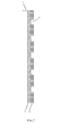
FIG. 1 is a structural schematic diagram of a touch-control screen according to an embodiment of the present utility model; -
FIG. 2 is a structural schematic diagram of a cross-section of a touch-control panel according to an embodiment of the present utility model; and -
FIG. 3 is a structural schematic diagram of a bottom plane of a touch-control panel according to an embodiment of the present utility model. - The following clearly and completely describes the technical solutions in the embodiments of the present utility model with reference to the accompanying drawings in the embodiments of the present utility model. Apparently, the described embodiments are merely a part rather than all of the embodiments of the present utility model. All other embodiments obtained by persons of ordinary skill in the art based on the embodiments of the present utility model without creative efforts shall fall within the protection scope of the present utility model.
- An embodiment of the present utility model provides a touch-control screen. As shown in
FIG. 1 , the touch-control screen includes: a metal frame 1, aliquid crystal display 2 embedded into the metal frame 1, and a touch-control panel 3 covering theliquid crystal display 2, where the touch-control panel 3 includes a transparent conductive shield layer, and the touch-control screen is characterized in that the transparent conductive shield layer is electrically connected to the metal frame. - The metal frame 1 is arranged on the outer side of the
liquid crystal display 2 to support and protect theliquid crystal display 2; and the touch-control panel 3 covers theliquid crystal display 2 and forms an enclosed structure with the metal frame 1, so that theliquid crystal display 2 is sealed in the structure. Therefore, the electromagnetic interference generated by theliquid crystal display 2 is sealed in the enclosed structure formed by the metal frame 1 and the touch-control panel 3, may only radiate into the metal frame 1 or the touch-control panel 3, and may not directly radiate out of the enclosed structure. - Because the metal frame 1 is connected to a ground cable of an electronic device where the touch-control screen is located, and in the embodiment of the present utility model, the transparent conductive shield layer in the touch-
control panel 3 is electrically connected to the metal frame 1, so that the transparent conductive shield layer is also connected to the ground cable of the electronic device to form a shielded body. In this case, the electromagnetic interference generated on the top surface of theliquid crystal display 2 is absorbed by the transparent conductive shield layer in the touch-control panel 3 and is led to the ground cable. Therefore, the electromagnetic interference is prevented from penetrating the touch-control panel to interfere the touch-control panel and the electronic device. The electromagnetic interference generated on the lateral surface and the bottom surface of theliquid crystal display 2 is absorbed by the metal frame 1 and led to the ground cable. After the transparent conductive shield layer is electrically connected to the metal frame 1, the touch-control panel 3 and the metal frame 1 form an integrated structure that absorbs electromagnetic interference, where the structure encloses theliquid crystal display 2 inside, thereby effectively shielding the electromagnetic interference generated by theliquid crystal display 2. - In the touch-control screen provided by the embodiment of the present utility model, the transparent conductive shield layer in the touch-control panel and the metal frame are electrically connected. Therefore, the touch-control panel and the metal frame form an integrated structure that absorbs electromagnetic interference, which effectively shields the electromagnetic interference generated by the liquid crystal display. Also, compared with electromagnetic interference shielding manners in the prior art, the utility model has the benefits of simple processing techniques for manufacturing the shielding structure and low costs.
- Further, in the embodiment of the present utility model, as shown in
FIG. 1 andFIG. 2 , the touch-control screen 3 further includes a silicondioxide shield layer 6 arranged in the touch-control panel 3 at an end near theliquid crystal display 2, the transparentconductive shield layer 5 is arranged on the silicondioxide shield layer 6 at an end far away from theliquid crystal display 2, the silicondioxide shield layer 6 has through-holes 4, and the transparentconductive shield layer 5 is electrically connected to the metal frame 1 through the through-holes 4. - The touch-
control panel 3 adopts a multi-layered structure which implements the touch-control function of the touch-control panel. In the multi-layered structure of the touch-control panel, the silicondioxide shield layer 6 is arranged at the bottom, and the transparentconductive shield layer 5 is arranged on the silicondioxide shield layer 6. In the embodiment of the present utility model, the through-holes 4 are formed on the surface of the silicondioxide shield layer 6, and the through-holes 4 penetrate the upper and lower surfaces of the silicondioxide shield layer 6, so that part of the transparentconductive shield layer 5 arranged in the silicondioxide shield layer 6 exposed out of the silicondioxide shield layer 6 at the outermost layer of the touch-control panel 3. The exposed points of the transparentconductive shield layer 5 are connected to the metal frame 1 to achieve electric connection between the transparentconductive shield layer 5 and the metal frame 1 through the through-holes 4. - Optionally, the transparent conductive shield layer may be electrically connected to the metal frame through conductive adhesive or conductive foam. The exposed points of the transparent conductive shield layer may be electrically connected to the metal frame in an electroplating manner, and the exposed points of the transparent conductive shield layer may be connected to the metal frame through other transparent conductive materials, where one end of a conductive material is connected to the exposed points of the transparent conductive shield layer and the other end of the conductive material may be connected to the side wall on the inner wall of the metal frame, and the conductive material is arranged in a place other than that of the liquid crystal display, so that the arrangement of the liquid crystal display is not affected.
- Further, in the embodiment of the present utility model, as shown in
FIG. 3 , the silicondioxide shield layer 6 has a plurality of through-holes, so that the transparentconductive shield layer 5 has a plurality of exposed points. Among the plurality of through-holes, the distance between two adjacent through-holes is the product of a wavelength of interference electromagnetic waves of the liquid crystal display and 1/20. If the wavelength of interference electromagnetic waves of the liquid crystal display is λ, set the distance between two adjacent through-holes 4 to be λ/20. Setting the distance between two adjacent through-holes 4 to be 1/20 of the interference wavelength may improve the shielding effect of the transparent conductive shield layer and prevent the leakage of interference electromagnetic waves. - Further, in the embodiment of the present utility model, the through-holes are arranged near an edge of the silicon dioxide shield layer. The through-holes are arranged in a position near the four edges of the silicon dioxide shield layer, so that the length of a conductive material used for connecting the exposed points of the transparent
conductive shield layer 5 and the metal frame is shortened to lower the costs. Meanwhile, the position of the conductive material may be near the edge of the touch-control panel to reduce the affect caused by the conductive material on the light transmission of the touch-control panel. - Further, in the embodiment of the present utility model, the distance between the positions of the through-
holes 4 and the edge of the silicondioxide shield layer 6 is greater than or equal to the creepage distance of test voltage when a static test is performed on the touch-control screen. When a static test is performed on the touch-control screen provided by the embodiment of the present utility model, static electricity may directly act on the exposed points of the transparentconductive shield layer 5 through the edge of the touch-control panel to damage the touch-control panel, and therefore, in the present utility model, the distance between the through-holes 4 and the edge of the silicondioxide shield layer 6 is set to be greater than or equal to the creepage distance of test voltage when the static test is performed. In this case, during the static test, the test voltage may not directly act on the exposed points of the transparentconductive shield layer 5 through the edge of the silicondioxide shield layer 6, preventing the damage caused by static electricity on the touch-control panel. - An embodiment of the present utility model provides a mobile communications device which includes the touch-control screen provided by the foregoing embodiments. After the touch-control screen provided by the present utility model is arranged on the mobile communications device, the electromagnetic interference generated by the liquid crystal display is effectively prevented from interfering with antennas of the mobile communications device.
- In the touch-control screen and the mobile communications device provided by the embodiments of the present utility model, the through-holes are arranged on the surface of the silicon dioxide shield layer, so that part of the transparent conductive shield layer is exposed out of the touch-control panel. By connecting the exposed points of the transparent conductive shield layer to the metal frame, the transparent conductive shield layer and the metal frame are electrically connected, and further, the touch-control panel and the metal frame form an integrated structure that absorbs electromagnetic interference, thereby effectively shielding electromagnetic interference generated by the liquid crystal display. Also, compared with electromagnetic interference shielding manners in the prior art, the utility model has the benefits of simple processing techniques for manufacturing the shielding structure and low costs.
- The foregoing descriptions are merely specific embodiments of the present utility model, but are not intended to limit the protection scope of the present utility model. Any variation or replacement readily figured out by persons skilled in the art within the technical scope disclosed in the present utility model shall fall within the protection scope of the present utility model. Therefore, the protection scope of the present utility model shall be subject to the protection scope of the claims.
Claims (7)
- A touch-control screen, comprising: a metal frame, a liquid crystal display embedded into the metal frame, and a touch-control panel covering the liquid crystal display, wherein the touch-control panel comprises a transparent conductive shield layer, and the touch-control screen is characterized in that the transparent conductive shield layer is electrically connected to the metal frame.
- The touch-control screen according to claim 1, wherein the touch-control panel further comprises a silicon dioxide shield layer arranged in the touch-control panel at an end near the liquid crystal display, the transparent conductive shield layer is arranged on the silicon dioxide shield layer at an end far away from the liquid crystal display, the silicon dioxide shield layer has a plurality of through-holes; and the transparent conductive shield layer is electrically connected to the metal frame through the through-holes.
- The touch-control screen according to claim 2, wherein the silicon dioxide shield layer has the plurality of through-holes, and among the plurality of through-holes, a distance between two adj acent through-holes is a product of a wavelength of interference electromagnetic waves of the liquid crystal display and 1/20.
- The touch-control screen according to claim 3, wherein the plurality of through-holes are located near an edge of the silicon dioxide shield layer.
- The touch-control screen according to claim 4, wherein the distance between the plurality of through-holes and the edge of the silicon dioxide shield layer is greater than or equal to a creepage distance of test voltage when a static test is performed on the touch-control screen.
- The touch-control screen according to any one of claims 1 to 5, wherein the transparent conductive shield layer is connected to the metal frame through conductive adhesive or conductive foam.
- A mobile communications device, comprising the touch-control screen according to claims 1 to 5.
Applications Claiming Priority (1)
| Application Number | Priority Date | Filing Date | Title |
|---|---|---|---|
| CN2012204424502U CN202795296U (en) | 2012-08-31 | 2012-08-31 | Touch display screen and mobile communication equipment |
Publications (2)
| Publication Number | Publication Date |
|---|---|
| EP2703964A1 true EP2703964A1 (en) | 2014-03-05 |
| EP2703964B1 EP2703964B1 (en) | 2017-11-22 |
Family
ID=47822522
Family Applications (1)
| Application Number | Title | Priority Date | Filing Date |
|---|---|---|---|
| EP13179396.0A Active EP2703964B1 (en) | 2012-08-31 | 2013-08-06 | Touch-control screen and mobile communications device |
Country Status (5)
| Country | Link |
|---|---|
| US (1) | US20140063362A1 (en) |
| EP (1) | EP2703964B1 (en) |
| JP (1) | JP5732699B2 (en) |
| CN (1) | CN202795296U (en) |
| WO (1) | WO2014032561A1 (en) |
Cited By (2)
| Publication number | Priority date | Publication date | Assignee | Title |
|---|---|---|---|---|
| EP3142185A4 (en) * | 2014-06-11 | 2017-06-28 | Huawei Technologies Co. Ltd. | Sensitive screen, control circuit thereof, control method therefor, and sensitive screen apparatus |
| CN120522923A (en) * | 2025-06-05 | 2025-08-22 | 东莞市友联亨达光电有限公司 | An adaptive electromagnetic shielding touch display module |
Families Citing this family (11)
| Publication number | Priority date | Publication date | Assignee | Title |
|---|---|---|---|---|
| CN202795296U (en) * | 2012-08-31 | 2013-03-13 | 华为终端有限公司 | Touch display screen and mobile communication equipment |
| KR102179329B1 (en) * | 2013-11-28 | 2020-11-18 | 삼성디스플레이 주식회사 | Display device |
| CN104852743B (en) * | 2015-04-16 | 2018-07-17 | 深圳市海浦蒙特科技有限公司 | Absolute value encoder signal processing apparatus and method |
| KR102326122B1 (en) * | 2015-09-03 | 2021-11-12 | 동우 화인켐 주식회사 | Touch panel and image display device comprising the same |
| CN106782080A (en) * | 2017-01-10 | 2017-05-31 | 奇酷互联网络科技(深圳)有限公司 | A kind of display device and the electronic product including it |
| CN106842672B (en) * | 2017-04-19 | 2019-07-26 | 京东方科技集团股份有限公司 | A kind of display device |
| CN109213351A (en) * | 2017-07-03 | 2019-01-15 | 深圳市鸿合创新信息技术有限责任公司 | A kind of electronic whiteboard touching device and electronic whiteboard |
| US10678343B2 (en) | 2018-03-19 | 2020-06-09 | Microsoft Technology Licensing, Llc | Passive mechanical keyboard |
| CN109917577B (en) * | 2019-01-31 | 2021-10-22 | 南京巨鲨显示科技有限公司 | Anti-electromagnetic interference portable display |
| CN114002873B (en) * | 2020-07-27 | 2024-01-23 | 北京小米移动软件有限公司 | Electronic device, control method thereof, and computer-readable storage medium |
| CN114006960B (en) * | 2020-07-28 | 2023-04-28 | 华为技术有限公司 | Electronic equipment |
Citations (5)
| Publication number | Priority date | Publication date | Assignee | Title |
|---|---|---|---|---|
| US6555743B1 (en) * | 2000-08-04 | 2003-04-29 | Dell Products L.P. | EMI attenuation obtained by application of waveguide beyond frequency cutoff techniques for add-in ITE mass storage devices |
| US20100215931A1 (en) * | 2007-12-10 | 2010-08-26 | Jau-Jier Chu | ITO layer structure |
| CN201590065U (en) * | 2010-02-02 | 2010-09-22 | 中兴通讯股份有限公司 | A display component and electronic equipment using the display component |
| WO2011017039A2 (en) * | 2009-08-03 | 2011-02-10 | 3M Innovative Properties Company | Antireflective transparent emi shielding optical filter |
| US20120087065A1 (en) * | 2010-10-06 | 2012-04-12 | Moon Kim | Shielding structures for wireless electronic devices with displays |
Family Cites Families (11)
| Publication number | Priority date | Publication date | Assignee | Title |
|---|---|---|---|---|
| JP2002341372A (en) * | 2001-05-21 | 2002-11-27 | Kyocera Corp | Liquid crystal display device and portable terminal equipment |
| EP1537767B1 (en) * | 2003-07-02 | 2008-12-03 | Siemens Home and Office Communications Devices GmbH & Co. KG | Shielding for emi-endangered electronic components and/or circuits of electronic devices |
| US8031273B2 (en) * | 2004-09-17 | 2011-10-04 | Sharp Kabushiki Kaisha | Display device, viewing angle control device, and electronic device |
| CN101458601B (en) * | 2007-12-14 | 2012-03-14 | 清华大学 | Touch screen and display device |
| JP2009204996A (en) * | 2008-02-28 | 2009-09-10 | Brother Ind Ltd | Image input and output device and operation device |
| JP5337061B2 (en) * | 2009-02-20 | 2013-11-06 | セイコーインスツル株式会社 | Touch panel and display device including the same |
| CN101825963B (en) * | 2009-03-03 | 2012-02-01 | 瀚宇彩晶股份有限公司 | Embedded touch input display panel |
| TWI375369B (en) * | 2009-12-11 | 2012-10-21 | Delta Electronics Inc | Socket device having grounding structure, application of socket device and manufacturing method thereof |
| JP2012027622A (en) * | 2010-07-21 | 2012-02-09 | Nissha Printing Co Ltd | Capacitance touch sensor and liquid crystal display device having capacitance touch input function |
| TWI523180B (en) * | 2012-05-07 | 2016-02-21 | 友達光電股份有限公司 | Touch panel, touch display panel and touch display apparatus |
| CN202795296U (en) * | 2012-08-31 | 2013-03-13 | 华为终端有限公司 | Touch display screen and mobile communication equipment |
-
2012
- 2012-08-31 CN CN2012204424502U patent/CN202795296U/en not_active Expired - Lifetime
-
2013
- 2013-08-06 EP EP13179396.0A patent/EP2703964B1/en active Active
- 2013-08-06 US US13/960,152 patent/US20140063362A1/en not_active Abandoned
- 2013-08-27 WO PCT/CN2013/082323 patent/WO2014032561A1/en not_active Ceased
- 2013-09-02 JP JP2013180955A patent/JP5732699B2/en active Active
Patent Citations (5)
| Publication number | Priority date | Publication date | Assignee | Title |
|---|---|---|---|---|
| US6555743B1 (en) * | 2000-08-04 | 2003-04-29 | Dell Products L.P. | EMI attenuation obtained by application of waveguide beyond frequency cutoff techniques for add-in ITE mass storage devices |
| US20100215931A1 (en) * | 2007-12-10 | 2010-08-26 | Jau-Jier Chu | ITO layer structure |
| WO2011017039A2 (en) * | 2009-08-03 | 2011-02-10 | 3M Innovative Properties Company | Antireflective transparent emi shielding optical filter |
| CN201590065U (en) * | 2010-02-02 | 2010-09-22 | 中兴通讯股份有限公司 | A display component and electronic equipment using the display component |
| US20120087065A1 (en) * | 2010-10-06 | 2012-04-12 | Moon Kim | Shielding structures for wireless electronic devices with displays |
Cited By (4)
| Publication number | Priority date | Publication date | Assignee | Title |
|---|---|---|---|---|
| EP3142185A4 (en) * | 2014-06-11 | 2017-06-28 | Huawei Technologies Co. Ltd. | Sensitive screen, control circuit thereof, control method therefor, and sensitive screen apparatus |
| US10530040B2 (en) | 2014-06-11 | 2020-01-07 | Huawei Technologies Co., Ltd. | Sensing screen, control circuit and control method thereof, and sensing screen apparatus |
| US11199917B2 (en) | 2014-06-11 | 2021-12-14 | Huawei Technologies Co., Ltd. | Sensing screen, control circuit and control method thereof, and sensing screen apparatus |
| CN120522923A (en) * | 2025-06-05 | 2025-08-22 | 东莞市友联亨达光电有限公司 | An adaptive electromagnetic shielding touch display module |
Also Published As
| Publication number | Publication date |
|---|---|
| WO2014032561A1 (en) | 2014-03-06 |
| JP5732699B2 (en) | 2015-06-10 |
| EP2703964B1 (en) | 2017-11-22 |
| JP2014049769A (en) | 2014-03-17 |
| CN202795296U (en) | 2013-03-13 |
| US20140063362A1 (en) | 2014-03-06 |
Similar Documents
| Publication | Publication Date | Title |
|---|---|---|
| US20140063362A1 (en) | Touch-Control Screen and Mobile Communications Device | |
| CN206274709U (en) | One kind electromagnetic shielding optical module | |
| WO2012009588A3 (en) | Integrated shielding for a package-on-package system | |
| CN102608781A (en) | Liquid crystal display (LCD) module and LCD | |
| CN102636671B (en) | Anechoic chamber with low frequency shielding property | |
| CN205491646U (en) | Insulating box of electromagnetic shield | |
| CN204795969U (en) | Electromagnetic shield glass structure with prevent function of drenching with rain | |
| CN202422013U (en) | Low-radiation keyboard | |
| CN203386179U (en) | Protection cover plate and touch screen with protection cover plate | |
| CN102612307B (en) | One easily welds radome | |
| CN205946502U (en) | Flexible circuit board and display device | |
| CN204103439U (en) | A kind of communication cable-end radome | |
| CN201213164Y (en) | Earthing construction improvement for flexible flat cable | |
| US20150355682A1 (en) | Low-Force Gap-Filling Conductive Structures | |
| CN204031722U (en) | Electromagnetic protection case | |
| CN202626085U (en) | Aluminum foil adhesive tape | |
| CN202373803U (en) | Shielding device of video graphics array (VGA) plug | |
| CN207252142U (en) | A kind of Transparent shielding cover for pcb board | |
| CN223180775U (en) | Avoidance structure for preventing upper iron frame from being in point contact conduction with silver paste of display screen | |
| CN105283055B (en) | A kind of anti-electromagnetic radiation device | |
| CN206743768U (en) | A kind of integrally stretching formula shielding case structure | |
| CN102833991B (en) | A kind of protection lid of printed circuit board | |
| CN201821636U (en) | Magnetic shielding device | |
| CN203924846U (en) | A kind of shielding house | |
| CN104563576A (en) | Shielded room |
Legal Events
| Date | Code | Title | Description |
|---|---|---|---|
| 17P | Request for examination filed |
Effective date: 20130806 |
|
| AK | Designated contracting states |
Kind code of ref document: A1 Designated state(s): AL AT BE BG CH CY CZ DE DK EE ES FI FR GB GR HR HU IE IS IT LI LT LU LV MC MK MT NL NO PL PT RO RS SE SI SK SM TR |
|
| AX | Request for extension of the european patent |
Extension state: BA ME |
|
| PUAI | Public reference made under article 153(3) epc to a published international application that has entered the european phase |
Free format text: ORIGINAL CODE: 0009012 |
|
| GRAP | Despatch of communication of intention to grant a patent |
Free format text: ORIGINAL CODE: EPIDOSNIGR1 |
|
| STAA | Information on the status of an ep patent application or granted ep patent |
Free format text: STATUS: GRANT OF PATENT IS INTENDED |
|
| RIC1 | Information provided on ipc code assigned before grant |
Ipc: G06F 1/18 20060101ALI20170517BHEP Ipc: G06F 3/041 20060101AFI20170517BHEP Ipc: G02F 1/1333 20060101ALN20170517BHEP |
|
| INTG | Intention to grant announced |
Effective date: 20170531 |
|
| GRAS | Grant fee paid |
Free format text: ORIGINAL CODE: EPIDOSNIGR3 |
|
| GRAA | (expected) grant |
Free format text: ORIGINAL CODE: 0009210 |
|
| STAA | Information on the status of an ep patent application or granted ep patent |
Free format text: STATUS: THE PATENT HAS BEEN GRANTED |
|
| RAP1 | Party data changed (applicant data changed or rights of an application transferred) |
Owner name: HUAWEI DEVICE (DONGGUAN) CO., LTD. |
|
| AK | Designated contracting states |
Kind code of ref document: B1 Designated state(s): AL AT BE BG CH CY CZ DE DK EE ES FI FR GB GR HR HU IE IS IT LI LT LU LV MC MK MT NL NO PL PT RO RS SE SI SK SM TR |
|
| REG | Reference to a national code |
Ref country code: GB Ref legal event code: FG4D |
|
| REG | Reference to a national code |
Ref country code: CH Ref legal event code: EP |
|
| REG | Reference to a national code |
Ref country code: IE Ref legal event code: FG4D |
|
| REG | Reference to a national code |
Ref country code: AT Ref legal event code: REF Ref document number: 948975 Country of ref document: AT Kind code of ref document: T Effective date: 20171215 |
|
| REG | Reference to a national code |
Ref country code: DE Ref legal event code: R096 Ref document number: 602013029694 Country of ref document: DE |
|
| REG | Reference to a national code |
Ref country code: NL Ref legal event code: MP Effective date: 20171122 |
|
| REG | Reference to a national code |
Ref country code: LT Ref legal event code: MG4D |
|
| REG | Reference to a national code |
Ref country code: AT Ref legal event code: MK05 Ref document number: 948975 Country of ref document: AT Kind code of ref document: T Effective date: 20171122 |
|
| PG25 | Lapsed in a contracting state [announced via postgrant information from national office to epo] |
Ref country code: ES Free format text: LAPSE BECAUSE OF FAILURE TO SUBMIT A TRANSLATION OF THE DESCRIPTION OR TO PAY THE FEE WITHIN THE PRESCRIBED TIME-LIMIT Effective date: 20171122 Ref country code: SE Free format text: LAPSE BECAUSE OF FAILURE TO SUBMIT A TRANSLATION OF THE DESCRIPTION OR TO PAY THE FEE WITHIN THE PRESCRIBED TIME-LIMIT Effective date: 20171122 Ref country code: NL Free format text: LAPSE BECAUSE OF FAILURE TO SUBMIT A TRANSLATION OF THE DESCRIPTION OR TO PAY THE FEE WITHIN THE PRESCRIBED TIME-LIMIT Effective date: 20171122 Ref country code: FI Free format text: LAPSE BECAUSE OF FAILURE TO SUBMIT A TRANSLATION OF THE DESCRIPTION OR TO PAY THE FEE WITHIN THE PRESCRIBED TIME-LIMIT Effective date: 20171122 Ref country code: NO Free format text: LAPSE BECAUSE OF FAILURE TO SUBMIT A TRANSLATION OF THE DESCRIPTION OR TO PAY THE FEE WITHIN THE PRESCRIBED TIME-LIMIT Effective date: 20180222 Ref country code: LT Free format text: LAPSE BECAUSE OF FAILURE TO SUBMIT A TRANSLATION OF THE DESCRIPTION OR TO PAY THE FEE WITHIN THE PRESCRIBED TIME-LIMIT Effective date: 20171122 |
|
| PG25 | Lapsed in a contracting state [announced via postgrant information from national office to epo] |
Ref country code: LV Free format text: LAPSE BECAUSE OF FAILURE TO SUBMIT A TRANSLATION OF THE DESCRIPTION OR TO PAY THE FEE WITHIN THE PRESCRIBED TIME-LIMIT Effective date: 20171122 Ref country code: RS Free format text: LAPSE BECAUSE OF FAILURE TO SUBMIT A TRANSLATION OF THE DESCRIPTION OR TO PAY THE FEE WITHIN THE PRESCRIBED TIME-LIMIT Effective date: 20171122 Ref country code: GR Free format text: LAPSE BECAUSE OF FAILURE TO SUBMIT A TRANSLATION OF THE DESCRIPTION OR TO PAY THE FEE WITHIN THE PRESCRIBED TIME-LIMIT Effective date: 20180223 Ref country code: BG Free format text: LAPSE BECAUSE OF FAILURE TO SUBMIT A TRANSLATION OF THE DESCRIPTION OR TO PAY THE FEE WITHIN THE PRESCRIBED TIME-LIMIT Effective date: 20180222 Ref country code: AT Free format text: LAPSE BECAUSE OF FAILURE TO SUBMIT A TRANSLATION OF THE DESCRIPTION OR TO PAY THE FEE WITHIN THE PRESCRIBED TIME-LIMIT Effective date: 20171122 Ref country code: HR Free format text: LAPSE BECAUSE OF FAILURE TO SUBMIT A TRANSLATION OF THE DESCRIPTION OR TO PAY THE FEE WITHIN THE PRESCRIBED TIME-LIMIT Effective date: 20171122 |
|
| REG | Reference to a national code |
Ref country code: FR Ref legal event code: PLFP Year of fee payment: 6 |
|
| PG25 | Lapsed in a contracting state [announced via postgrant information from national office to epo] |
Ref country code: SK Free format text: LAPSE BECAUSE OF FAILURE TO SUBMIT A TRANSLATION OF THE DESCRIPTION OR TO PAY THE FEE WITHIN THE PRESCRIBED TIME-LIMIT Effective date: 20171122 Ref country code: EE Free format text: LAPSE BECAUSE OF FAILURE TO SUBMIT A TRANSLATION OF THE DESCRIPTION OR TO PAY THE FEE WITHIN THE PRESCRIBED TIME-LIMIT Effective date: 20171122 Ref country code: DK Free format text: LAPSE BECAUSE OF FAILURE TO SUBMIT A TRANSLATION OF THE DESCRIPTION OR TO PAY THE FEE WITHIN THE PRESCRIBED TIME-LIMIT Effective date: 20171122 Ref country code: CY Free format text: LAPSE BECAUSE OF FAILURE TO SUBMIT A TRANSLATION OF THE DESCRIPTION OR TO PAY THE FEE WITHIN THE PRESCRIBED TIME-LIMIT Effective date: 20171122 Ref country code: CZ Free format text: LAPSE BECAUSE OF FAILURE TO SUBMIT A TRANSLATION OF THE DESCRIPTION OR TO PAY THE FEE WITHIN THE PRESCRIBED TIME-LIMIT Effective date: 20171122 |
|
| REG | Reference to a national code |
Ref country code: DE Ref legal event code: R097 Ref document number: 602013029694 Country of ref document: DE |
|
| PG25 | Lapsed in a contracting state [announced via postgrant information from national office to epo] |
Ref country code: RO Free format text: LAPSE BECAUSE OF FAILURE TO SUBMIT A TRANSLATION OF THE DESCRIPTION OR TO PAY THE FEE WITHIN THE PRESCRIBED TIME-LIMIT Effective date: 20171122 Ref country code: IT Free format text: LAPSE BECAUSE OF FAILURE TO SUBMIT A TRANSLATION OF THE DESCRIPTION OR TO PAY THE FEE WITHIN THE PRESCRIBED TIME-LIMIT Effective date: 20171122 Ref country code: SM Free format text: LAPSE BECAUSE OF FAILURE TO SUBMIT A TRANSLATION OF THE DESCRIPTION OR TO PAY THE FEE WITHIN THE PRESCRIBED TIME-LIMIT Effective date: 20171122 Ref country code: PL Free format text: LAPSE BECAUSE OF FAILURE TO SUBMIT A TRANSLATION OF THE DESCRIPTION OR TO PAY THE FEE WITHIN THE PRESCRIBED TIME-LIMIT Effective date: 20171122 |
|
| PLBE | No opposition filed within time limit |
Free format text: ORIGINAL CODE: 0009261 |
|
| STAA | Information on the status of an ep patent application or granted ep patent |
Free format text: STATUS: NO OPPOSITION FILED WITHIN TIME LIMIT |
|
| 26N | No opposition filed |
Effective date: 20180823 |
|
| PG25 | Lapsed in a contracting state [announced via postgrant information from national office to epo] |
Ref country code: SI Free format text: LAPSE BECAUSE OF FAILURE TO SUBMIT A TRANSLATION OF THE DESCRIPTION OR TO PAY THE FEE WITHIN THE PRESCRIBED TIME-LIMIT Effective date: 20171122 |
|
| PG25 | Lapsed in a contracting state [announced via postgrant information from national office to epo] |
Ref country code: MC Free format text: LAPSE BECAUSE OF FAILURE TO SUBMIT A TRANSLATION OF THE DESCRIPTION OR TO PAY THE FEE WITHIN THE PRESCRIBED TIME-LIMIT Effective date: 20171122 |
|
| REG | Reference to a national code |
Ref country code: CH Ref legal event code: PL |
|
| PG25 | Lapsed in a contracting state [announced via postgrant information from national office to epo] |
Ref country code: LU Free format text: LAPSE BECAUSE OF NON-PAYMENT OF DUE FEES Effective date: 20180806 Ref country code: CH Free format text: LAPSE BECAUSE OF NON-PAYMENT OF DUE FEES Effective date: 20180831 Ref country code: LI Free format text: LAPSE BECAUSE OF NON-PAYMENT OF DUE FEES Effective date: 20180831 |
|
| REG | Reference to a national code |
Ref country code: BE Ref legal event code: MM Effective date: 20180831 |
|
| REG | Reference to a national code |
Ref country code: IE Ref legal event code: MM4A |
|
| REG | Reference to a national code |
Ref country code: DE Ref legal event code: R081 Ref document number: 602013029694 Country of ref document: DE Owner name: HUAWEI DEVICE CO., LTD., DONGGUAN, CN Free format text: FORMER OWNER: HUAWEI DEVICE (DONGGUAN) CO., LTD., DONGGUAN, GUANGDONG, CN |
|
| PG25 | Lapsed in a contracting state [announced via postgrant information from national office to epo] |
Ref country code: IE Free format text: LAPSE BECAUSE OF NON-PAYMENT OF DUE FEES Effective date: 20180806 |
|
| PG25 | Lapsed in a contracting state [announced via postgrant information from national office to epo] |
Ref country code: BE Free format text: LAPSE BECAUSE OF NON-PAYMENT OF DUE FEES Effective date: 20180831 |
|
| PG25 | Lapsed in a contracting state [announced via postgrant information from national office to epo] |
Ref country code: MT Free format text: LAPSE BECAUSE OF NON-PAYMENT OF DUE FEES Effective date: 20180806 |
|
| PG25 | Lapsed in a contracting state [announced via postgrant information from national office to epo] |
Ref country code: TR Free format text: LAPSE BECAUSE OF FAILURE TO SUBMIT A TRANSLATION OF THE DESCRIPTION OR TO PAY THE FEE WITHIN THE PRESCRIBED TIME-LIMIT Effective date: 20171122 |
|
| PG25 | Lapsed in a contracting state [announced via postgrant information from national office to epo] |
Ref country code: PT Free format text: LAPSE BECAUSE OF FAILURE TO SUBMIT A TRANSLATION OF THE DESCRIPTION OR TO PAY THE FEE WITHIN THE PRESCRIBED TIME-LIMIT Effective date: 20171122 Ref country code: HU Free format text: LAPSE BECAUSE OF FAILURE TO SUBMIT A TRANSLATION OF THE DESCRIPTION OR TO PAY THE FEE WITHIN THE PRESCRIBED TIME-LIMIT; INVALID AB INITIO Effective date: 20130806 |
|
| PG25 | Lapsed in a contracting state [announced via postgrant information from national office to epo] |
Ref country code: MK Free format text: LAPSE BECAUSE OF NON-PAYMENT OF DUE FEES Effective date: 20171122 |
|
| PG25 | Lapsed in a contracting state [announced via postgrant information from national office to epo] |
Ref country code: AL Free format text: LAPSE BECAUSE OF FAILURE TO SUBMIT A TRANSLATION OF THE DESCRIPTION OR TO PAY THE FEE WITHIN THE PRESCRIBED TIME-LIMIT Effective date: 20171122 Ref country code: IS Free format text: LAPSE BECAUSE OF FAILURE TO SUBMIT A TRANSLATION OF THE DESCRIPTION OR TO PAY THE FEE WITHIN THE PRESCRIBED TIME-LIMIT Effective date: 20180322 |
|
| PGFP | Annual fee paid to national office [announced via postgrant information from national office to epo] |
Ref country code: DE Payment date: 20250702 Year of fee payment: 13 |
|
| PGFP | Annual fee paid to national office [announced via postgrant information from national office to epo] |
Ref country code: GB Payment date: 20250703 Year of fee payment: 13 |
|
| PGFP | Annual fee paid to national office [announced via postgrant information from national office to epo] |
Ref country code: FR Payment date: 20250703 Year of fee payment: 13 |