EP2701198A2 - Device with strained layer for quantum well confinement and method for manufacturing thereof - Google Patents
Device with strained layer for quantum well confinement and method for manufacturing thereof Download PDFInfo
- Publication number
- EP2701198A2 EP2701198A2 EP13170002.3A EP13170002A EP2701198A2 EP 2701198 A2 EP2701198 A2 EP 2701198A2 EP 13170002 A EP13170002 A EP 13170002A EP 2701198 A2 EP2701198 A2 EP 2701198A2
- Authority
- EP
- European Patent Office
- Prior art keywords
- layer
- strain
- channel
- quantum barrier
- relaxed buffer
- Prior art date
- Legal status (The legal status is an assumption and is not a legal conclusion. Google has not performed a legal analysis and makes no representation as to the accuracy of the status listed.)
- Withdrawn
Links
Images



Classifications
-
- H—ELECTRICITY
- H10—SEMICONDUCTOR DEVICES; ELECTRIC SOLID-STATE DEVICES NOT OTHERWISE PROVIDED FOR
- H10D—INORGANIC ELECTRIC SEMICONDUCTOR DEVICES
- H10D30/00—Field-effect transistors [FET]
- H10D30/60—Insulated-gate field-effect transistors [IGFET]
- H10D30/62—Fin field-effect transistors [FinFET]
-
- B—PERFORMING OPERATIONS; TRANSPORTING
- B82—NANOTECHNOLOGY
- B82Y—SPECIFIC USES OR APPLICATIONS OF NANOSTRUCTURES; MEASUREMENT OR ANALYSIS OF NANOSTRUCTURES; MANUFACTURE OR TREATMENT OF NANOSTRUCTURES
- B82Y10/00—Nanotechnology for information processing, storage or transmission, e.g. quantum computing or single electron logic
-
- H—ELECTRICITY
- H10—SEMICONDUCTOR DEVICES; ELECTRIC SOLID-STATE DEVICES NOT OTHERWISE PROVIDED FOR
- H10D—INORGANIC ELECTRIC SEMICONDUCTOR DEVICES
- H10D30/00—Field-effect transistors [FET]
- H10D30/40—FETs having zero-dimensional [0D], one-dimensional [1D] or two-dimensional [2D] charge carrier gas channels
- H10D30/43—FETs having zero-dimensional [0D], one-dimensional [1D] or two-dimensional [2D] charge carrier gas channels having one-dimensional [1D] charge carrier gas channels, e.g. quantum wire FETs or transistors having 1D quantum-confined channels
-
- H—ELECTRICITY
- H10—SEMICONDUCTOR DEVICES; ELECTRIC SOLID-STATE DEVICES NOT OTHERWISE PROVIDED FOR
- H10D—INORGANIC ELECTRIC SEMICONDUCTOR DEVICES
- H10D30/00—Field-effect transistors [FET]
- H10D30/40—FETs having zero-dimensional [0D], one-dimensional [1D] or two-dimensional [2D] charge carrier gas channels
- H10D30/47—FETs having zero-dimensional [0D], one-dimensional [1D] or two-dimensional [2D] charge carrier gas channels having two-dimensional [2D] charge carrier gas channels, e.g. nanoribbon FETs or high electron mobility transistors [HEMT]
- H10D30/471—High electron mobility transistors [HEMT] or high hole mobility transistors [HHMT]
- H10D30/472—High electron mobility transistors [HEMT] or high hole mobility transistors [HHMT] having lower bandgap active layer formed on top of wider bandgap layer, e.g. inverted HEMT
-
- H—ELECTRICITY
- H10—SEMICONDUCTOR DEVICES; ELECTRIC SOLID-STATE DEVICES NOT OTHERWISE PROVIDED FOR
- H10D—INORGANIC ELECTRIC SEMICONDUCTOR DEVICES
- H10D30/00—Field-effect transistors [FET]
- H10D30/60—Insulated-gate field-effect transistors [IGFET]
- H10D30/751—Insulated-gate field-effect transistors [IGFET] having composition variations in the channel regions
-
- H—ELECTRICITY
- H10—SEMICONDUCTOR DEVICES; ELECTRIC SOLID-STATE DEVICES NOT OTHERWISE PROVIDED FOR
- H10D—INORGANIC ELECTRIC SEMICONDUCTOR DEVICES
- H10D62/00—Semiconductor bodies, or regions thereof, of devices having potential barriers
- H10D62/80—Semiconductor bodies, or regions thereof, of devices having potential barriers characterised by the materials
- H10D62/82—Heterojunctions
- H10D62/822—Heterojunctions comprising only Group IV materials heterojunctions, e.g. Si/Ge heterojunctions
-
- H—ELECTRICITY
- H10—SEMICONDUCTOR DEVICES; ELECTRIC SOLID-STATE DEVICES NOT OTHERWISE PROVIDED FOR
- H10D—INORGANIC ELECTRIC SEMICONDUCTOR DEVICES
- H10D62/00—Semiconductor bodies, or regions thereof, of devices having potential barriers
- H10D62/80—Semiconductor bodies, or regions thereof, of devices having potential barriers characterised by the materials
- H10D62/83—Semiconductor bodies, or regions thereof, of devices having potential barriers characterised by the materials being Group IV materials, e.g. B-doped Si or undoped Ge
- H10D62/832—Semiconductor bodies, or regions thereof, of devices having potential barriers characterised by the materials being Group IV materials, e.g. B-doped Si or undoped Ge being Group IV materials comprising two or more elements, e.g. SiGe
Definitions
- the present invention relates to a FinFET device or a planar FET device comprising a semiconductor substrate, a strain-relaxed buffer layer comprising Ge, a strained quantum barrier layer comprising SiGe and a channel layer, wherein the strained quantum barrier layer is positioned in between the strain relaxed buffer layer and the channel layer and in physical contact with both.
- compositions of the strain-relaxed buffer layer, the strained quantum barrier layer and the channel layer are chosen such that a band offset of the channel layer and a band offset of the strained quantum barrier layer with respect to the strain-relaxed buffer layer are of opposite signs, thereby creating a quantum well effect in a conduction band structure by creating a conduction band offset between the channel and the quantum barrier layer for a n-type device and, respectively, in a valence band structure by creating a valence band offset between the channel and the quantum barrier layer for a p-type device, thereby improving carrier confinement in the channel.
- the present invention relates to a FinFET device or a planar FET device as described in the appended claims.
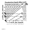
- FIG 1A represents the lines of equal conduction band offset for the different compositions of the SRB layer (or the substrate) and the channel layer (dark lines on grey area) and the lines of equal conduction band offset for the different compositions of the SRB layer (or the substrate) and the strained quantum barrier (QB) layer (dark lines on white area) for a FinFET device.
- QB strained quantum barrier
- FIG 1B shows on the left the stacks of layers corresponding to the full squares denoted with A, B, C, D in FIG 1A , while on the right are the stacks according to the invention comprising a strained quantum barrier layer which introduces an additional conduction band offset between the channel and the underlying layers as illustrated by the open squares in FIG 1A .
- FIG 2A represents the lines of equal valence band offset for the different compositions of the SRB layer (or the substrate) and the channel layer (dark lines on grey area) and the lines of equal valence band offset for the different compositions of the SRB layer (or the substrate) and the strained quantum barrier (QB) layer (dark lines on white area) for a FinFET device.
- QB strained quantum barrier
- FIG 2B represents on the left the stacks of layers corresponding to the full squares denoted with A, B, C, D in FIG 2A , while on the right are the stacks according to the invention comprising a strained quantum barrier layer which introduces an additional valence band offset between the channel and the underlying layers as illustrated by the open squares in FIG 2A .
- FIG 3 represents the lines of equal conduction band offset for the different compositions of the SRB layer (or the substrate) and the channel layer (dark lines on grey area) and the lines of equal conduction band offset for the different compositions of the SRB layer (or the substrate) and the strained quantum barrier (QB) layer (dark lines on white area) for a planar nFET device.
- QB strained quantum barrier
- FIG 4 represents the lines of equal valence band offset for the different compositions of the SRB layer (or the substrate) and the channel layer (grey area) and the lines of equal valence band offset for the different compositions of the SRB layer (or the substrate) and the strained quantum barrier (QB) layer (white area) for a planar pFET device.
- QB strained quantum barrier
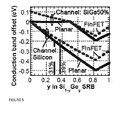
- FIG. 5 shows the conduction band offset between channel and SRB versus Ge% in the SRB for Si and SiGe50% channels.
- FIG. 6 shows the valence band offset between channel and SRB versus Ge% in the SRB for Ge and SiGe50% channels.
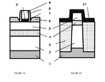
- FIG. 7A represents schematically a cross section along the channel of a planar device according to an embodiment of the invention.
- FIG. 7B represents schematically a cross section across the fin of a FinFET device according to an embodiment of the invention.
- the invention relates to a device with strained layer for quantum well confinement and a method for manufacturing thereof.
- the device of the invention has improved performance for the 10 nm-node FinFETs.
- both the channel stress (determining the channel mobility) and the band offset between channel and the underlying layers (determining the electrostatic control of the MOSFET) is determined by the channel and SRB composition.
- One drawback of this approach is that higher strain is beneficial both for high mobility and band offset, but too high strain leads to defect formation and relaxation.
- the device of the disclosure solves at least the above mentioned problem and allows increasing the band offset without increasing the strain to a level which can lead to defect formation and relaxation in the channel.
- a quantum barrier layer as disclosed in the present invention both parameters are decoupled: the channel stress is determined by the composition choice for the channel and the SRB, whereas the band offset between channel and the underlying layers is determined by the composition choice for the channel and the quantum barrier layer. This stack therefore allows separate optimization of channel stress and band offset.
- a FinFET device which comprises: a semiconductor substrate, a strain-relaxed buffer (SRB) layer, a strained quantum barrier layer (SQB) and a channel layer, wherein the strained quantum barrier layer is positioned in between the strain relaxed buffer layer and the channel layer and in physical contact with both, and wherein the compositions of the strain-relaxed buffer layer, the strained quantum barrier layer and the channel layer are chosen such that a band offset of the channel layer and a band offset of the strained quantum barrier layer with respect to the strain-relaxed buffer layer are of opposite signs, thereby creating a quantum well effect in a conduction band structure for a n-type FinFET device and, respectively, in a valence band structure for a p-type FinFET device, thereby improving carrier confinement in the channel.
- Both the strained quantum barrier layer and the channel layer are strained with respect to the strain relaxed buffer.
- the strain tensor ⁇ ' is calculated along the ⁇ 011> direction on a (100) wafer, per standard transistor orientation. For wide, planar FETs, a strained channel on an SRB is under biaxial stress, while for FinFETs, the stress is effectively uniaxial.
- the strain tensor ⁇ ' is then rotated to ⁇ along the semiconductor's principal axes. From ⁇ , the bands for the channel and SRB are calculated with parameters from Van De Walle et al., Phys. Rev. B39, 1871(1989 ) and Galdin et al, Semicond. Sci. Technol. 15, 565 (2000 ) for Si 1-x Ge x .
- the effect of strain on the conduction band energy is calculated through deformation potential theory, including the ⁇ and L bands for Si 1-x Ge x .
- the valence band structure is calculated by 6-band k.p theory for all semiconductors, using parameters from Van De Walle et al., Phys.Rev. B 39,1871 (1989 ) .
- Deformation potentials are linearly interpolated for alloys.
- FIG 1A represents the lines of equal conduction band offset for different compositions of the SRB layer (or the substrate) Si 1-y Ge y and the channel layer Si 1-x Ge x (dark lines on grey area) and the lines of equal conduction band offset for the different compositions of the SRB layer (or the substrate) Si 1-y Ge y and the strained quantum barrier (QB) layer (dark lines on white area) Si 1-x Ge x for a FinFET device.
- QB strained quantum barrier
- FIG 1B shows on the left the stacks of layers corresponding to the full squares denoted with A, B, C, D in FIG 1A , while on the right are the stacks according to the invention comprising a strained quantum barrier (SQB or QB) layer which introduces an additional conduction band offset between the channel and the underlying layers as illustrated by the open squares in FIG 1A .
- SQL strained quantum barrier
- the final stack consists of Si substrate, QB layer made of SiGe50%, Channel layer made of Si.
- FIG 2A represents the lines of equal valence band offset for the different compositions of the SRB layer (or the substrate) Si 1-y Ge y and the channel layer Si 1-x Ge x (dark lines on grey area) and the lines of equal valence band offset for the different compositions of the SRB layer (or the substrate) Si 1-y Ge y and the strained quantum barrier (QB) layer Si 1-x Ge x (dark lines on white area) for a FinFET device.
- QB strained quantum barrier
- FIG 2B represents on the left the stacks of layers corresponding to the full squares denoted with A, B, C, D in FIG 2A , while on the right are the stacks according to the invention comprising a strained quantum barrier layer which introduces an additional valence band offset between the channel and the underlying layers as illustrated by the open squares in FIG 2A .
- the final stack consists of SRB made of Ge, QB layer made of SiGe50, channel layer made of Ge.
- this example corresponds to a situation wherein according to the model no QB solution is available for the initial stack (SiGe40% channel on Si substrate) with a valence band offset of +250meV.
- the semiconductor substrate comprises/consist of a group IV semiconductor material.
- the strain-relaxed buffer layer comprises Ge and the strained quantum barrier layer comprising SiGe.
- the channel of the FinFET device comprises Ge.
- the compositions of the strain-relaxed buffer layer, the strained quantum barrier layer and the channel layer are chosen such that between the strained quantum barrier layer and the channel layer there is a lattice constant mismatch of at least about 0.4% .
- the device of the first example and the manufacturing thereof is described in detail further. It is an advantage of the method of the invention that the whole stack, i.e. the SRB, the SQB and the channel layer can be grown in-situ, in one process step.
- the compositions of the strain-relaxed buffer layer, the strained quantum barrier layer and the channel layer are chosen such that the strained quantum barrier layer comprises a lower amount of Ge than the strain relaxed buffer.
- the strained quantum barrier layer comprises 10% to 70% less Ge than the strain-relaxed buffer.
- the strained quantum barrier layer comprises at least 10% less Ge than the strain-relaxed buffer in order to achieve the quantum well effect. At maximum the strained quantum barrier layer comprises about 70% less Ge to achieve the quantum well effect and without introducing defects due to lattice mismatch.
- At least one of the strain-relaxed buffer layer and the channel layer may further comprise Si .
- at least one or both the SRB layer and the channel layer comprise SiGe.
- at least one or both the SRB layer and the channel layer consist of SiGe.
- At least one of the strain-relaxed buffer layer and the channel layer may further comprise Sn .
- at least one or both the SRB layer and the channel layer comprise GeSn.
- at least one or both the SRB layer and the channel layer consist of GeSn.
- the channel of the FinFET device consists of Si.
- the compositions of the strain-relaxed buffer layer, the strained quantum barrier layer and the channel layer are chosen such that the strained quantum barrier layer comprises a higher amount of Ge than the strain-relaxed buffer.
- the strained quantum barrier layer comprises 10% to 70% more Ge than the strain-relaxed buffer.
- the strained quantum barrier layer comprises at least 10% more Ge than the strain-relaxed buffer in order to achieve the quantum well effect.
- the strained quantum barrier layer comprises about 70% more Ge to achieve the quantum well effect without introducing defects due to lattice mismatch.
- the strained quantum barrier layer which is part of the FinFET device has a thickness from 3 nm to 30 nm, more preferably between 5nm and 20nm.
- a planar FET device comprising : a semiconductor substrate, a strain-relaxed buffer (SRB) layer, a strained quantum barrier layer (SQB) and a channel layer, wherein the strained quantum barrier layer is positioned in between the strain relaxed buffer layer and the channel layer and in physical contact with both, and wherein the compositions of the strain-relaxed buffer layer, the strained quantum barrier layer and the channel layer are chosen such that a band offset of the channel layer and a band offset of the strained quantum barrier layer with respect to the strain-relaxed buffer layer are of opposite signs thereby creating a quantum well effect in a conduction band structure by creating a conduction band offset between the channel and the quantum barrier layer for a n-type FET device and, respectively, in a valence band structure by creating a valence band offset between the channel and the quantum barrier layer for a p-type FET device, thereby improving carrier confinement in the channel.
- SRB strain-relaxed buffer
- SQL strained quantum barrier
- the semiconductor substrate comprises/consist of a group IV semiconductor material.
- the strain-relaxed buffer layer comprises Ge and the strained quantum barrier layer comprising SiGe. Further, in embodiments of the second aspect the channel layer comprises Ge.
- FIG 3 represents the lines of equal conduction band offset for the different compositions of the SRB layer (or the substrate) Si 1-y Ge y and the channel layer Si 1-x Ge x (dark lines on grey area) and the lines of equal conduction band offset for the different compositions of the SRB layer (or the substrate) Si 1-y Ge y and the strained quantum barrier (QB) layer Si 1-x Ge x (dark lines on white area) for a planar nFET device.
- QB strained quantum barrier
- the device is a n-type planar FET and the compositions of the strain-relaxed buffer layer, the strained quantum barrier layer and the channel layer are chosen such that between the strained quantum barrier layer and the channel layer there is a lattice constant mismatch of at least about 0.4%.
- At least one of the strain-relaxed buffer layer and the channel layer may further comprise Si.
- at least one or both the SRB layer and the channel layer comprise SiGe.
- at least one or both the SRB layer and the channel layer consist of SiGe.
- At least one of the strain-relaxed buffer layer and the channel layer may further comprise Sn.
- at least one or both the SRB layer and the channel layer comprise GeSn.
- at least one or both the SRB layer and the channel layer consist of GeSn.
- FIG 4 represents the lines of equal valence band offset for the different compositions of the SRB layer (or the substrate) Si 1-y Ge y and the channel layer Si 1-x Ge x (dark lines on grey area) and the lines of equal valence band offset for the different compositions of the SRB layer (or the substrate) Si 1-y Ge y and the strained quantum barrier (QB) layer Si 1-x Ge x (dark lines on white area) for a planar pFET device.
- QB strained quantum barrier
- the device is a p-type planar FET and the compositions of the strain-relaxed buffer layer, the strained quantum barrier layer and the channel layer are chosen such that the strained quantum barrier layer comprises a lower amount of Ge than the strain relaxed buffer.
- the strained quantum barrier layer comprises 10% to 70% less Ge than the strain-relaxed buffer.
- the strained quantum barrier layer comprises at least 10% less Ge than the strain-relaxed buffer in order to achieve the quantum well effect.
- the strained quantum barrier layer comprises about 70% less Ge to achieve the quantum well effect without introducing defects due to lattice mismatch.
- the strained quantum barrier layer which is part of the planar FET device has a thickness from 3nm to 30 nm, more preferably between 5nm and 20nm.
- Offsets are 25% lower for nFinFETs than for planar nFETs (as shown in FIG 5 ), e.g., a -200 meV offset in a strained-Si nFET requires an SRB with 31% Ge for planar vs. 39% Ge for fins.
- ⁇ EV is 10% higher for fins than for planar (as shown in FIG. 6 ).
- Certain embodiments of the first and second aspect relate to an nFET device comprising a strained layer for quantum well confinement. Further certain embodiments relate to an nFET device having improved channel mobility and ON-current and/or lower leakage than the state of the art devices.
- the nFET device comprises a Ge-rich channel and a silicon germanium strained quantum barrier layer.
- Certain embodiments relate to a method of manufacturing for an nFET device comprising a strained layer for quantum well confinement.
- nFET performance enhancement is replacing silicon as channel material in traditional Si nFET with Germanium or Germanium rich SiGe with/without the addition of Sn because of the higher mobility of these materials compared with Si.
- a transistor is formed on a stack comprising a thick (about 200nm) relaxed SiGeSn layer grown on a silicon wafer.
- nFET performance enhancement is enhancing the mobility by creating a tensile stress in the channel. This is achieved by e.g. forming a GeSn relaxed buffer in between the Si substrate and the channel.
- the channel may comprise Ge, Ge-rich SiGe or SiGeSn.
- both options referred to above i.e. the thick relaxed SiGeSn and the strained SiGeSn channel on top of a relaxed GeSn layer have important drawbacks such as: (1) the band gap of the whole structure is small leading to unwanted junction leakage; (2) there is small or no conduction band offset between the channel and the substrate which leads to deteriorated short-channel effects.
- a thin, strained quantum barrier (SQB) layer comprising SiGe and positioned just under the channel provides the required conduction band offset, leading to better short-channel effects.
- the SQB layer in one embodiment has the required conduction band offset both for the planar nFETs and n-type FinFET configurations.
- the SQB layer has a larger band gap than the underlying strain-relaxed buffer which leads to a decrease of the overall junction leakage.
- n-FET transistor comprising:
- SRB strain-relaxed buffer
- strained quantum barrier (SQB) layer comprising SiGe
- the strained quantum barrier layer is positioned in between the strain-relaxed buffer layer and the channel layer and in physical contact with both
- compositions of the strain-relaxed buffer layer (SRB), the strained quantum barrier layer and the channel layer are chosen such that between the strained quantum barrier layer and the channel layer there is a lattice constant mismatch of at least about 0.4%.
- the semiconductor substrate is silicon
- each of the strain-relaxed buffer layer and the channel layer has a Ge concentration higher than or equal to about 75 at%.
- both are either Ge-rich layers or, in specific embodiments, pure Ge layers.
- a strain-relaxed layer is a layer which is substantially free of mechanical stress and mechanical strain.
- the composition of the layer to be grown and the parameters of the growth process such as e.g. growth temperature, a certain thickness is required before the relaxation appears (critical thickness). In case of a Ge-rich layer grown on Si substrate the critical thickness is estimated to be less than about 30 nm.
- strain-relaxed buffer layer and/or the channel layer can further comprise Si up to about 25 at%.
- composition of the SRB layer and the channel can be similar or even identical, such as for example in the embodiments wherein both SRB layer and the channel layer are made of SiGe (with Ge > about 75 at%).
- a SRB layer and channel layer made both of the same material has the advantage of easier manufacturability.
- the strain-relaxed buffer layer and/or the channel layer further comprises Sn.
- the SRB and/or the channel comprises GeSn or SiGeSn with a Sn concentration lower than about 10 at%.
- the SRB comprises GeSn while the channel layer comprises SiGe or GeSn or SiGeSn, each of these compositions having a Ge concentration higher than or equal to about 75 at%. In case of GeSn the concentration of Ge is even higher up to about 90 at%.
- the strained quantum barrier layer is a strained layer for quantum well confinement.
- the SQB layer in one embodiment comprises SiGe, more preferably consists of SiGe and dopants.
- the concentration of Ge in the SQB layer is between about 50 at% to 90 at%. Particularly the Ge concentration may be between about 60 at% to 80 at%, more particularly between about65 at% and 75 at%.
- the SQB layer may contain only Si and Ge within the concentration ranges mentioned above, e.g., does not contain any other elements except dopants, which have a typical dopant level concentration (about 1 at%).
- the optimum composition of the SQB layer is chosen in function of the composition of the channel layer such that a lattice constant mismatch or about 0.4% (or about 0.03 nm) is introduced between the SQB layer and the channel layer.
- the lattice constant mismatch is appreciated based on the absolute values of the lattice constants for the different compositions, as known for a corresponding blanket layer in relaxed state.
- the channel layer comprises Ge or SiGe (Ge > about 75 at%) a concentration of about 65 at%-90 at% Ge in the SQB layer is optimal, as it leads to the highest band offset, around 100mV.
- a difference in Ge concentration of about 10 at% between the Ge concentration of the SRB layer and the Ge concentration of the channel layer (overlying the SRB layer) is considered to be optimal in case the channel layer contains only Ge or SiGe without other elements except dopants.
- the optimum Ge concentration of the SQB layer underneath is lower, namely from about 50 at% to about 70 at%.
- band gap of the SiGe SQB layer about 1eV is predicted, which is significantly higher than the 0.67eV or lower for the Ge/GeSn layers.
- the thickness of the SQB layer is chosen to be between about 3 nm and 30nm, such that the SQB layer remain strained and prevent forming defects due to stress relaxation,
- the relaxation behavior of layers grown in trenches (recesses) as in one embodiment is different than in the case of layers deposited on blanket substrates wherein a critical thickness can be estimated more straightforward.
- the strain-relaxed buffer layer, the strained quantum barrier layer and possibly the channel layer may comprise dopants at a dopant level concentration of about 1 at%.
- the device in one embodiment can comprise elevated source and drain areas made of germanium or SiGe, wherein SiGe has a Si concentration lower than the Si concentration of the strain-relaxed buffer layer.
- the strain-relaxed buffer layer comprises a plurality of sub-layers.
- a gradient in Ge concentration can be introduced at the epitaxial growth, typically from a Si-rich SiGe at the bottom of the SRB layer in contact with the substrate to a Ge -rich SiGe at the interface with the SQB layer.
- FIG. 7A represents schematically a cross section along the channel of a planar device according to an embodiment of the disclosure, wherein: (1) substrate; (2) SRB layer; (4) SQB layer; (5) channel layer; (6) elevated S/D; (7') gate metal; (8) spacers; (9) gate fill.
- the channel layer has a thickness of about 3nm to 20nm.
- FIG. 7B represents schematically a cross section across the fin of a FinFET device according to an embodiment of the disclosure, wherein: (1) substrate; (2) SRB layer; (3) isolation; (4) SQB layer; (5) channel layer; (7") gate metal.
- the strained quantum barrier layer (4) may be positioned within about 10nm below the lowest part of the gate electrode (7").
- the channel layer has a thickness of about 10nm to 50 nm.
- a method for manufacturing a n-FET transistor comprising:
- a strained quantum barrier SQB layer which is overlying and in contact with the strain-relaxed buffer layer and comprises SiGe, followed by
- compositions of the strain-relaxed buffer layer, the strained quantum barrier layer and the channel layer are chosen such that between the strained quantum barrier layer and the channel layer there is a lattice constant mismatch of at least about 0.4%.
- the strain-relaxed buffer layer is grown epitaxial in the recess thereby filling completely and overgrowing the initial recess. Then, well implantation can be performed. Subsequently, the strain-relaxed buffer is partially recessed back (etched back) before forming the strained quantum barrier layer, such that a second recess is left having a smaller depth than the initial recess. The SRB is thus filling only partially the initial recess and after growing the SQB layer and the channel layer the initial recess is filled up completely again.
- the strained quantum barrier layer and the channel layer are grown epitaxial in-situ (without vacuum break) in an epitaxial reactor.
- the process of etching back the SRB layer may be performed in-situ in the epitaxial reactor, immediately before growing the SQB layer.
- the strain-relaxed buffer layer, the quantum barrier layer and the channel layer may comprise dopants introduced either during the epitaxial growth by in-situ doping or by implantation after the epitaxial growth.
- an nFET transistor comprising a Si substrate, a SRB layer on the Si substrate and a channel layer, wherein both the SRB layer and the channel layer are made of Ge and may comprise dopants. Further the transistor comprises a SQB layer sandwiched in between the SRB layer and the channel layer and in physical contact with both.
- the SQB layer is contains SiGe (with about 75at% Ge) and may further contain dopants.
- the device of this example has the benefit of the reduced junction leakage due to the presence higher band gap of the SQB layer.
- an nFET transistor comprising a Si substrate, a SRB layer on the Si substrate made of GeSn with up to about 10 at% Sn and which may comprise further dopants. Further the transistor comprises a channel layer made of GeSn (Sn ⁇ about 10 at%) or SiGe (Ge > about 75at%) and may comprise dopants. Further, the transistor comprises a SQB layer sandwiched in between the SRB layer and the channel layer and in physical contact with both. The SQB layer contains SiGe (with about 60-70 at% Ge) and may further contain dopants.
- the device of this example has the benefit of the reduced junction leakage due to the presence of the SQB layer. Additionally, the transistor has the benefit of enhanced mobility and, consequently, higher ON-current due to the tensile strain present in the channel.
- An n-FET transistor comprising a semiconductor substrate, a strain-relaxed buffer layer comprising Ge, a strained quantum barrier layer comprising SiGe and a channel layer comprising Ge, wherein the strained quantum barrier layer is positioned in between the strain relaxed buffer layer and the channel layer and in physical contact with both, and wherein the compositions of the strain-relaxed buffer layer, the strained quantum barrier layer and the channel layer are chosen such that between the strained quantum barrier layer and the channel layer there is a lattice constant mismatch of at least about 0.4 %.
- each of the strain-relaxed buffer layer and the channel layer has a Ge concentration higher than or equal to about 75 at%.
- strain-relaxed buffer layer and/or the channel layer further comprises Si.
- strain-relaxed buffer layer and/or the channel layer further comprises Sn.
- n-FET transistor of the above wherein the Sn concentration is lower than about 10 at%.
- the quantum barrier layer comprises SiGe with a Ge concentration between about 50 at% to 90 at%, particularly between about 60 at% to 80 at%, more particularly between about 65 at% and 75 at%.
- n-FET transistor of any of the above, wherein one of more of the strain-relaxed buffer, the quantum barrier layer and the channel layer comprises dopants.
- n-FET transistor of any of the above further comprising elevated source and drain areas comprising Ge or SiGe with a Si concentration lower than the Si concentration of the strain-relaxed buffer.
- strain-relaxed buffer layer comprises a plurality of sub-layers and/or wherein the strain-relaxed buffer has a gradient in Ge concentration with the lowest Ge concentration at the interface with the substrate.
- n-FET transistor of any of the above, wherein the transistor has a planar configuration.
- n-FET transistor of the above wherein the channel layer has a thickness of about 3nm to 20nm.
- n-FET transistor of the above wherein the transistor has a FinFET configuration.
- n-FET transistor of the above wherein the transistor has a FinFET configuration and the channel layer has a thickness of about 10nm to 50 nm.
- a method for manufacturing an n-FET transistor comprises a) providing a patterned semiconductor substrate having a recess exposing at its bottom the semiconductor substrate and having lateral walls comprising an insulator material, b) forming by epitaxial growth a strain-relaxed buffer layer comprising Ge in the recess, followed by c) forming by epitaxial growth a strained quantum barrier layer which is overlying and in contact with the strain-relaxed buffer layer and comprises SiGe, followed by d) forming by epitaxial growth a channel layer which is overlying and in contact with the strained quantum barrier layer and comprises Ge, wherein the compositions of the strain-relaxed buffer layer, the strained quantum barrier layer and the channel layer are chosen such that between the strained quantum barrier layer and the channel layer there is a lattice constant mismatch of at least about 0.4%.
- each of the strain-relaxed buffer layer and the channel layer have a Ge concentration higher than or equal to about 75 at%.
- strain-relaxed buffer layer and the channel layer further comprises Si.
- strain-relaxed buffer layer and the channel layer further comprises Sn.
- the quantum barrier layer comprises SiGe with a Ge concentration between about 50 at% to 90 at%, particularly between about 60 at% to 80 at%, more particularly between about 65 at% and 75at%.
- one or more of the strain-relaxed buffer, the quantum barrier layer and the channel layer comprises dopants introduced during the epitaxial growth by in-situ doping or by implantation after the epitaxial growth.
- strain-relaxed buffer layer comprises a plurality of sub-layers and/or wherein the strain-relaxed buffer has a gradient in Ge concentration with the lowest Ge concentration at the interface with the substrate.
Landscapes
- Engineering & Computer Science (AREA)
- Chemical & Material Sciences (AREA)
- Nanotechnology (AREA)
- Physics & Mathematics (AREA)
- Mathematical Physics (AREA)
- Theoretical Computer Science (AREA)
- Crystallography & Structural Chemistry (AREA)
- Insulated Gate Type Field-Effect Transistor (AREA)
- Thin Film Transistor (AREA)
- Metal-Oxide And Bipolar Metal-Oxide Semiconductor Integrated Circuits (AREA)
Abstract
Description
- Several options are being considered for further performance enhancement of FinFETs and planar FET devices. Among them, replacing the traditional channel material (Si) or using channel stress to enhance the mobility are solutions known in the art. For example, as shown by Eneman et. al. at IEEE International Electron Device Meeting p. 131 (2012 ) heterostructures of strained SiGe channels on a strain-relaxed buffer can deliver efficient mobility boosts due to strain.
- However such methods have often important drawbacks such as unwanted junction leakage and deteriorated short-channel effects.
- The present invention relates to a FinFET device or a planar FET device comprising a semiconductor substrate, a strain-relaxed buffer layer comprising Ge, a strained quantum barrier layer comprising SiGe and a channel layer, wherein the strained quantum barrier layer is positioned in between the strain relaxed buffer layer and the channel layer and in physical contact with both. The compositions of the strain-relaxed buffer layer, the strained quantum barrier layer and the channel layer are chosen such that a band offset of the channel layer and a band offset of the strained quantum barrier layer with respect to the strain-relaxed buffer layer are of opposite signs, thereby creating a quantum well effect in a conduction band structure by creating a conduction band offset between the channel and the quantum barrier layer for a n-type device and, respectively, in a valence band structure by creating a valence band offset between the channel and the quantum barrier layer for a p-type device, thereby improving carrier confinement in the channel.
- Further the present invention relates to a FinFET device or a planar FET device as described in the appended claims.
- All drawings are intended to illustrate some aspects and embodiments of the present disclosure. The drawings described are only schematic and are non-limiting.
-
FIG 1A represents the lines of equal conduction band offset for the different compositions of the SRB layer (or the substrate) and the channel layer (dark lines on grey area) and the lines of equal conduction band offset for the different compositions of the SRB layer (or the substrate) and the strained quantum barrier (QB) layer (dark lines on white area) for a FinFET device. -
FIG 1B shows on the left the stacks of layers corresponding to the full squares denoted with A, B, C, D inFIG 1A , while on the right are the stacks according to the invention comprising a strained quantum barrier layer which introduces an additional conduction band offset between the channel and the underlying layers as illustrated by the open squares inFIG 1A . -
FIG 2A represents the lines of equal valence band offset for the different compositions of the SRB layer (or the substrate) and the channel layer (dark lines on grey area) and the lines of equal valence band offset for the different compositions of the SRB layer (or the substrate) and the strained quantum barrier (QB) layer (dark lines on white area) for a FinFET device. -
FIG 2B represents on the left the stacks of layers corresponding to the full squares denoted with A, B, C, D inFIG 2A , while on the right are the stacks according to the invention comprising a strained quantum barrier layer which introduces an additional valence band offset between the channel and the underlying layers as illustrated by the open squares inFIG 2A . -
FIG 3 represents the lines of equal conduction band offset for the different compositions of the SRB layer (or the substrate) and the channel layer (dark lines on grey area) and the lines of equal conduction band offset for the different compositions of the SRB layer (or the substrate) and the strained quantum barrier (QB) layer (dark lines on white area) for a planar nFET device. -
FIG 4 represents the lines of equal valence band offset for the different compositions of the SRB layer (or the substrate) and the channel layer (grey area) and the lines of equal valence band offset for the different compositions of the SRB layer (or the substrate) and the strained quantum barrier (QB) layer (white area) for a planar pFET device. -
FIG. 5 shows the conduction band offset between channel and SRB versus Ge% in the SRB for Si and SiGe50% channels. -
FIG. 6 shows the valence band offset between channel and SRB versus Ge% in the SRB for Ge and SiGe50% channels. -
FIG. 7A represents schematically a cross section along the channel of a planar device according to an embodiment of the invention. -
FIG. 7B represents schematically a cross section across the fin of a FinFET device according to an embodiment of the invention. - The invention relates to a device with strained layer for quantum well confinement and a method for manufacturing thereof. The device of the invention has improved performance for the 10 nm-node FinFETs.
- In a traditional layer stack where the channel is directly grown on top of an SRB, both the channel stress (determining the channel mobility) and the band offset between channel and the underlying layers (determining the electrostatic control of the MOSFET) is determined by the channel and SRB composition. One drawback of this approach is that higher strain is beneficial both for high mobility and band offset, but too high strain leads to defect formation and relaxation.
- The device of the disclosure solves at least the above mentioned problem and allows increasing the band offset without increasing the strain to a level which can lead to defect formation and relaxation in the channel. By introducing a quantum barrier layer as disclosed in the present invention both parameters are decoupled: the channel stress is determined by the composition choice for the channel and the SRB, whereas the band offset between channel and the underlying layers is determined by the composition choice for the channel and the quantum barrier layer. This stack therefore allows separate optimization of channel stress and band offset.
- Whereas scaling bulk silicon FinFETs requires ever increasing doping levels in the ground-plane, the use of heterojunctions provides an alternative to improve electrostatics. Indeed, simulations indicate that band offsets of 200 meV are sufficient to improve Drain-induced barrier lowering (DIBL) and subthreshold slope significantly for 10 nm-node FinFETs, with little further improvement for larger band offsets.
- In a first aspect of the invention a FinFET device is disclosed which comprises: a semiconductor substrate, a strain-relaxed buffer (SRB) layer, a strained quantum barrier layer (SQB) and a channel layer, wherein the strained quantum barrier layer is positioned in between the strain relaxed buffer layer and the channel layer and in physical contact with both, and wherein the compositions of the strain-relaxed buffer layer, the strained quantum barrier layer and the channel layer are chosen such that a band offset of the channel layer and a band offset of the strained quantum barrier layer with respect to the strain-relaxed buffer layer are of opposite signs, thereby creating a quantum well effect in a conduction band structure for a n-type FinFET device and, respectively, in a valence band structure for a p-type FinFET device, thereby improving carrier confinement in the channel. Both the strained quantum barrier layer and the channel layer are strained with respect to the strain relaxed buffer.
- The conduction and valence band offsets for SiGe heterostructures were calculated using a model briefly described below.
- First, the strain tensor ε' is calculated along the <011> direction on a (100) wafer, per standard transistor orientation. For wide, planar FETs, a strained channel on an SRB is under biaxial stress, while for FinFETs, the stress is effectively uniaxial. The strain tensor ε' is then rotated to ε along the semiconductor's principal axes. From ε, the bands for the channel and SRB are calculated with parameters from Van De Walle et al., Phys. Rev. B39, 1871(1989 ) and Galdin et al, Semicond. Sci. Technol. 15, 565 (2000 ) for Si1-xGex.
- A quantum well for nFETs corresponds to a negative conduction band offset ΔEC = EC,channel-EC,SRB, while pFETs require a positive valence band offset ΔEV = EV,channel-EV,SRB. The effect of strain on the conduction band energy is calculated through deformation potential theory, including the Δ and L bands for Si1-xGex. The valence band structure is calculated by 6-band k.p theory for all semiconductors, using parameters from Van De Walle et al., Phys.Rev. ). Deformation potentials are linearly interpolated for alloys. For an optimized gate stack (CET of 0.7 nm), work functions are estimated assuming a VT target of +0.2 and -0.2 V for respectively n- and pFETs.
-
FIG 1A represents the lines of equal conduction band offset for different compositions of the SRB layer (or the substrate) Si1-yGey and the channel layer Si1-xGex (dark lines on grey area) and the lines of equal conduction band offset for the different compositions of the SRB layer (or the substrate) Si1-yGey and the strained quantum barrier (QB) layer (dark lines on white area) Si1-xGex for a FinFET device. -
FIG 1B shows on the left the stacks of layers corresponding to the full squares denoted with A, B, C, D inFIG 1A , while on the right are the stacks according to the invention comprising a strained quantum barrier (SQB or QB) layer which introduces an additional conduction band offset between the channel and the underlying layers as illustrated by the open squares inFIG 1A . - From
FIG 1B several examples can be summarized: - (i) enhanced conduction band offset of -260meV composed of - 200meV for the initial stack (Si channel on SiGe40% SRB) and -60meV introduced by the strained quantum barrier layer. The final stack consists of SRB made of SiGe40%, QB layer made of SiGe80%, channel layer made of Si.
- (ii) enhanced conduction band offset of -210meV composed of - 120meV for the initial stack (Si channel on SiGe25% SRB) and -90meV introduced by the strained quantum barrier layer. The final stack consists of SRB made of SiGe25%, QB layer made of SiGe75%, channel layer made of Si.
- (iii) enhanced conduction band offset of -100meV composed of 0 meV for the initial stack (Si channel on Si substrate) and -100meV introduced by the strained quantum barrier layer. The final stack consists of Si substrate, QB layer made of SiGe50%, Channel layer made of Si.
- (iv) enhanced conduction band offset of -70meV composed of 0 meV for the initial stack (Ge channel on Ge SRB) and -70meV introduced by the strained quantum barrier layer. The final stack consists of SRB made of Ge, QB layer made of SiGe80%, Channel layer made of Ge.
-
FIG 2A represents the lines of equal valence band offset for the different compositions of the SRB layer (or the substrate) Si1-yGey and the channel layer Si1-xGex (dark lines on grey area) and the lines of equal valence band offset for the different compositions of the SRB layer (or the substrate) Si1-yGey and the strained quantum barrier (QB) layer Si1-xGex (dark lines on white area) for a FinFET device. -
FIG 2B represents on the left the stacks of layers corresponding to the full squares denoted with A, B, C, D inFIG 2A , while on the right are the stacks according to the invention comprising a strained quantum barrier layer which introduces an additional valence band offset between the channel and the underlying layers as illustrated by the open squares inFIG 2A . - From
FIG 2B several examples can be summarized: - (i) enhanced valence band offset of +150meV composed of 0 meV for the initial stack (Ge channel on Ge SRB) and +150meV introduced by the strained quantum barrier layer. The final stack consists of SRB made of Ge, QB layer made of SiGe50, channel layer made of Ge.
- (ii) enhanced valence band offset of +350meV composed of +170 meV for the initial stack (Ge channel on SiGe75% SRB) and +180meV introduced by the strained quantum barrier layer. The final stack consists of SRB made of SiGe75%, QB layer made of SiGe25%, channel layer made of Ge.
- (iii) enhanced valence band offset of +420meV composed of +250 meV for the initial stack (SiGe80% channel on SiGe40% SRB) and +170meV introduced by the strained quantum barrier layer. The final stack consists of SRB made of SiGe40%, QB layer made of Si, channel layer made of SiGe80%.
- (iv) this example corresponds to a situation wherein according to the model no QB solution is available for the initial stack (SiGe40% channel on Si substrate) with a valence band offset of +250meV.
- In embodiments of the first aspect the semiconductor substrate comprises/consist of a group IV semiconductor material.
- In different embodiments of the first aspect the strain-relaxed buffer layer comprises Ge and the strained quantum barrier layer comprising SiGe.
- Further in embodiments of the first aspect the channel of the FinFET device comprises Ge.
- In a first example wherein the device is a n-type FinFET and the channel layer comprises Ge, the compositions of the strain-relaxed buffer layer, the strained quantum barrier layer and the channel layer are chosen such that between the strained quantum barrier layer and the channel layer there is a lattice constant mismatch of at least about 0.4% .
- The device of the first example and the manufacturing thereof is described in detail further. It is an advantage of the method of the invention that the whole stack, i.e. the SRB, the SQB and the channel layer can be grown in-situ, in one process step.
- In a second example wherein the device is a p-type FinFET and the channel layer comprises Ge, the compositions of the strain-relaxed buffer layer, the strained quantum barrier layer and the channel layer are chosen such that the strained quantum barrier layer comprises a lower amount of Ge than the strain relaxed buffer. Preferably, the strained quantum barrier layer comprises 10% to 70% less Ge than the strain-relaxed buffer. Preferably the strained quantum barrier layer comprises at least 10% less Ge than the strain-relaxed buffer in order to achieve the quantum well effect. At maximum the strained quantum barrier layer comprises about 70% less Ge to achieve the quantum well effect and without introducing defects due to lattice mismatch.
- Further in embodiments of the first aspect related to the first or the second example, at least one of the strain-relaxed buffer layer and the channel layer may further comprise Si . Thus, at least one or both the SRB layer and the channel layer comprise SiGe. Preferably, at least one or both the SRB layer and the channel layer consist of SiGe.
- Alternatively, in embodiments of the first aspect related to the first or the second example, at least one of the strain-relaxed buffer layer and the channel layer may further comprise Sn . Thus, at least one or both the SRB layer and the channel layer comprise GeSn. Preferably, at least one or both the SRB layer and the channel layer consist of GeSn.
- Furthermore, in other embodiments of the first aspect wherein the strain-relaxed buffer layer comprises Ge and the strained quantum barrier layer comprising SiGe, the channel of the FinFET device consists of Si.
- In a third example of the first aspect wherein the device is a n-type FinFET and the channel layer consists of Si, the compositions of the strain-relaxed buffer layer, the strained quantum barrier layer and the channel layer are chosen such that the strained quantum barrier layer comprises a higher amount of Ge than the strain-relaxed buffer. Preferably, the strained quantum barrier layer comprises 10% to 70% more Ge than the strain-relaxed buffer. Preferably, the strained quantum barrier layer comprises at least 10% more Ge than the strain-relaxed buffer in order to achieve the quantum well effect. At maximum, the strained quantum barrier layer comprises about 70% more Ge to achieve the quantum well effect without introducing defects due to lattice mismatch.
- In different embodiments of the first aspect related to the first, second or third example, the strained quantum barrier layer which is part of the FinFET device has a thickness from 3 nm to 30 nm, more preferably between 5nm and 20nm.
- In a second aspect of the invention a planar FET device is disclosed comprising : a semiconductor substrate, a strain-relaxed buffer (SRB) layer, a strained quantum barrier layer (SQB) and a channel layer, wherein the strained quantum barrier layer is positioned in between the strain relaxed buffer layer and the channel layer and in physical contact with both, and wherein the compositions of the strain-relaxed buffer layer, the strained quantum barrier layer and the channel layer are chosen such that a band offset of the channel layer and a band offset of the strained quantum barrier layer with respect to the strain-relaxed buffer layer are of opposite signs thereby creating a quantum well effect in a conduction band structure by creating a conduction band offset between the channel and the quantum barrier layer for a n-type FET device and, respectively, in a valence band structure by creating a valence band offset between the channel and the quantum barrier layer for a p-type FET device, thereby improving carrier confinement in the channel. Both the strained quantum barrier layer and the channel layer are strained with respect to the strain relaxed buffer.
- In embodiments of the second aspect the semiconductor substrate comprises/consist of a group IV semiconductor material.
- In embodiments of the second aspect the strain-relaxed buffer layer comprises Ge and the strained quantum barrier layer comprising SiGe. Further, in embodiments of the second aspect the channel layer comprises Ge.
-
FIG 3 represents the lines of equal conduction band offset for the different compositions of the SRB layer (or the substrate) Si1-yGey and the channel layer Si1-xGex (dark lines on grey area) and the lines of equal conduction band offset for the different compositions of the SRB layer (or the substrate) Si1-yGey and the strained quantum barrier (QB) layer Si1-xGex (dark lines on white area) for a planar nFET device. - In a fourth example of the second aspect the device is a n-type planar FET and the compositions of the strain-relaxed buffer layer, the strained quantum barrier layer and the channel layer are chosen such that between the strained quantum barrier layer and the channel layer there is a lattice constant mismatch of at least about 0.4%.
- Further in embodiments of the second aspect related to the fourth example, at least one of the strain-relaxed buffer layer and the channel layer may further comprise Si. Thus, at least one or both the SRB layer and the channel layer comprise SiGe. Thus, at least one or both the SRB layer and the channel layer consist of SiGe.
- Yet further in other embodiments of the second aspect related to the fourth example, at least one of the strain-relaxed buffer layer and the channel layer may further comprise Sn. Thus, at least one or both the SRB layer and the channel layer comprise GeSn. Thus, at least one or both the SRB layer and the channel layer consist of GeSn.
- The device of the fourth example and the manufacturing thereof is discussed in detail further.
-
FIG 4 represents the lines of equal valence band offset for the different compositions of the SRB layer (or the substrate) Si1-yGey and the channel layer Si1-xGex (dark lines on grey area) and the lines of equal valence band offset for the different compositions of the SRB layer (or the substrate) Si1-yGey and the strained quantum barrier (QB) layer Si1-xGex (dark lines on white area) for a planar pFET device. - In a fifth example of the second aspect the device is a p-type planar FET and the compositions of the strain-relaxed buffer layer, the strained quantum barrier layer and the channel layer are chosen such that the strained quantum barrier layer comprises a lower amount of Ge than the strain relaxed buffer. Preferably, the strained quantum barrier layer comprises 10% to 70% less Ge than the strain-relaxed buffer. Preferably, the strained quantum barrier layer comprises at least 10% less Ge than the strain-relaxed buffer in order to achieve the quantum well effect. At maximum, the strained quantum barrier layer comprises about 70% less Ge to achieve the quantum well effect without introducing defects due to lattice mismatch.
- In different embodiments of the second aspect related to the fourth or the fifth example, the strained quantum barrier layer which is part of the planar FET device has a thickness from 3nm to 30 nm, more preferably between 5nm and 20nm.
- Offsets are 25% lower for nFinFETs than for planar nFETs (as shown in
FIG 5 ), e.g., a -200 meV offset in a strained-Si nFET requires an SRB with 31% Ge for planar vs. 39% Ge for fins. For Ge channel pFETs, ΔEV is 10% higher for fins than for planar (as shown inFIG. 6 ). - Certain embodiments of the first and second aspect relate to an nFET device comprising a strained layer for quantum well confinement. Further certain embodiments relate to an nFET device having improved channel mobility and ON-current and/or lower leakage than the state of the art devices.
- In specific embodiments the nFET device comprises a Ge-rich channel and a silicon germanium strained quantum barrier layer.
- Certain embodiments relate to a method of manufacturing for an nFET device comprising a strained layer for quantum well confinement.
- Several options are being considered for further nFET performance enhancement. One of them is replacing silicon as channel material in traditional Si nFET with Germanium or Germanium rich SiGe with/without the addition of Sn because of the higher mobility of these materials compared with Si. In an example, a transistor is formed on a stack comprising a thick (about 200nm) relaxed SiGeSn layer grown on a silicon wafer.
- Another option for further nFET performance enhancement is enhancing the mobility by creating a tensile stress in the channel. This is achieved by e.g. forming a GeSn relaxed buffer in between the Si substrate and the channel. The channel may comprise Ge, Ge-rich SiGe or SiGeSn.
- However, both options referred to above i.e. the thick relaxed SiGeSn and the strained SiGeSn channel on top of a relaxed GeSn layer have important drawbacks such as: (1) the band gap of the whole structure is small leading to unwanted junction leakage; (2) there is small or no conduction band offset between the channel and the substrate which leads to deteriorated short-channel effects.
- Certain embodiments relate to a solution which can solve at least one problem from those mentioned above. A thin, strained quantum barrier (SQB) layer comprising SiGe and positioned just under the channel provides the required conduction band offset, leading to better short-channel effects. Moreover, the SQB layer in one embodiment has the required conduction band offset both for the planar nFETs and n-type FinFET configurations.
- Advantageously, the SQB layer has a larger band gap than the underlying strain-relaxed buffer which leads to a decrease of the overall junction leakage.
- In one aspect an n-FET transistor is described comprising:
- - a semiconductor substrate,
- - a strain-relaxed buffer (SRB) layer comprising Ge,
- - a strained quantum barrier (SQB) layer comprising SiGe, and
- - a channel layer comprising Ge,
- - wherein the strained quantum barrier layer is positioned in between the strain-relaxed buffer layer and the channel layer and in physical contact with both, and
- - wherein the compositions of the strain-relaxed buffer layer (SRB), the strained quantum barrier layer and the channel layer are chosen such that between the strained quantum barrier layer and the channel layer there is a lattice constant mismatch of at least about 0.4%.
- In one embodiment, the semiconductor substrate is silicon.
- In one embodiment, each of the strain-relaxed buffer layer and the channel layer has a Ge concentration higher than or equal to about 75 at%. Thus both are either Ge-rich layers or, in specific embodiments, pure Ge layers. A strain-relaxed layer is a layer which is substantially free of mechanical stress and mechanical strain. Depending on the composition of the substrate, the substrate being patterned or non-patterned, the composition of the layer to be grown and the parameters of the growth process such as e.g. growth temperature, a certain thickness is required before the relaxation appears (critical thickness). In case of a Ge-rich layer grown on Si substrate the critical thickness is estimated to be less than about 30 nm.
- Further, the strain-relaxed buffer layer and/or the channel layer can further comprise Si up to about 25 at%.
- In particular embodiments the composition of the SRB layer and the channel can be similar or even identical, such as for example in the embodiments wherein both SRB layer and the channel layer are made of SiGe (with Ge > about 75 at%). A SRB layer and channel layer made both of the same material has the advantage of easier manufacturability.
- In another embodiment, the strain-relaxed buffer layer and/or the channel layer further comprises Sn. In one embodiment the SRB and/or the channel comprises GeSn or SiGeSn with a Sn concentration lower than about 10 at%.
- In an example the SRB comprises GeSn while the channel layer comprises SiGe or GeSn or SiGeSn, each of these compositions having a Ge concentration higher than or equal to about 75 at%. In case of GeSn the concentration of Ge is even higher up to about 90 at%.
- In another embodiment, the strained quantum barrier layer is a strained layer for quantum well confinement. The SQB layer in one embodiment comprises SiGe, more preferably consists of SiGe and dopants. The concentration of Ge in the SQB layer is between about 50 at% to 90 at%. Particularly the Ge concentration may be between about 60 at% to 80 at%, more particularly between about65 at% and 75 at%. The SQB layer may contain only Si and Ge within the concentration ranges mentioned above, e.g., does not contain any other elements except dopants, which have a typical dopant level concentration (about 1 at%).
- Further, the optimum composition of the SQB layer is chosen in function of the composition of the channel layer such that a lattice constant mismatch or about 0.4% (or about 0.03 nm) is introduced between the SQB layer and the channel layer. The lattice constant mismatch is appreciated based on the absolute values of the lattice constants for the different compositions, as known for a corresponding blanket layer in relaxed state.
- In examples where the channel layer comprises Ge or SiGe (Ge > about 75 at%) a concentration of about 65 at%-90 at% Ge in the SQB layer is optimal, as it leads to the highest band offset, around 100mV. As an indicative rule of thumb a difference in Ge concentration of about 10 at% between the Ge concentration of the SRB layer and the Ge concentration of the channel layer (overlying the SRB layer) is considered to be optimal in case the channel layer contains only Ge or SiGe without other elements except dopants.
- In examples where the channel layer comprises GeSn (Ge > about 75 at%) and considering the lowering effect that Sn has on the lattice constant, the optimum Ge concentration of the SQB layer underneath is lower, namely from about 50 at% to about 70 at%.
- For the band gap of the SiGe SQB layer about 1eV is predicted, which is significantly higher than the 0.67eV or lower for the Ge/GeSn layers.
- In one embodiment, the thickness of the SQB layer is chosen to be between about 3 nm and 30nm, such that the SQB layer remain strained and prevent forming defects due to stress relaxation, As known to the skilled in the art, the relaxation behavior of layers grown in trenches (recesses) as in one embodiment is different than in the case of layers deposited on blanket substrates wherein a critical thickness can be estimated more straightforward.
- In some embodiments of the disclosure the strain-relaxed buffer layer, the strained quantum barrier layer and possibly the channel layer may comprise dopants at a dopant level concentration of about 1 at%.
- Further, the device in one embodiment can comprise elevated source and drain areas made of germanium or SiGe, wherein SiGe has a Si concentration lower than the Si concentration of the strain-relaxed buffer layer.
- In one embodiment, the strain-relaxed buffer layer comprises a plurality of sub-layers. Within the SRB layer or its different sub-layers a gradient in Ge concentration can be introduced at the epitaxial growth, typically from a Si-rich SiGe at the bottom of the SRB layer in contact with the substrate to a Ge -rich SiGe at the interface with the SQB layer.
-
FIG. 7A represents schematically a cross section along the channel of a planar device according to an embodiment of the disclosure, wherein: (1) substrate; (2) SRB layer; (4) SQB layer; (5) channel layer; (6) elevated S/D; (7') gate metal; (8) spacers; (9) gate fill. - In the examples of the planar configuration the channel layer has a thickness of about 3nm to 20nm.
-
FIG. 7B represents schematically a cross section across the fin of a FinFET device according to an embodiment of the disclosure, wherein: (1) substrate; (2) SRB layer; (3) isolation; (4) SQB layer; (5) channel layer; (7") gate metal. - In the examples of the FinFET configuration the strained quantum barrier layer (4) may be positioned within about 10nm below the lowest part of the gate electrode (7").
- Further in the embodiments of the FinFET configuration the channel layer has a thickness of about 10nm to 50 nm.
- In a second aspect a method for manufacturing a n-FET transistor is described comprising:
- a. Providing a patterned semiconductor substrate having a recess exposing at its bottom the semiconductor substrate and having lateral walls comprising an insulator material, followed by
- b. Forming by epitaxial growth a strain-relaxed buffer SRB layer comprising Ge in the recess, then
- c. forming by epitaxial growth a strained quantum barrier SQB layer which is overlying and in contact with the strain-relaxed buffer layer and comprises SiGe, followed by
- d. forming by epitaxial growth a channel layer which is overlying and in contact with the strained quantum barrier layer, wherein the channel layer comprises Ge,
- e. wherein the compositions of the strain-relaxed buffer layer, the strained quantum barrier layer and the channel layer are chosen such that between the strained quantum barrier layer and the channel layer there is a lattice constant mismatch of at least about 0.4%.
- In one embodiment, the strain-relaxed buffer layer is grown epitaxial in the recess thereby filling completely and overgrowing the initial recess. Then, well implantation can be performed. Subsequently, the strain-relaxed buffer is partially recessed back (etched back) before forming the strained quantum barrier layer, such that a second recess is left having a smaller depth than the initial recess. The SRB is thus filling only partially the initial recess and after growing the SQB layer and the channel layer the initial recess is filled up completely again.
- In one embodiment, the strained quantum barrier layer and the channel layer are grown epitaxial in-situ (without vacuum break) in an epitaxial reactor. The process of etching back the SRB layer may be performed in-situ in the epitaxial reactor, immediately before growing the SQB layer.
- In one embodiment, the strain-relaxed buffer layer, the quantum barrier layer and the channel layer may comprise dopants introduced either during the epitaxial growth by in-situ doping or by implantation after the epitaxial growth.
- In a specific example an nFET transistor is described comprising a Si substrate, a SRB layer on the Si substrate and a channel layer, wherein both the SRB layer and the channel layer are made of Ge and may comprise dopants. Further the transistor comprises a SQB layer sandwiched in between the SRB layer and the channel layer and in physical contact with both. The SQB layer is contains SiGe (with about 75at% Ge) and may further contain dopants. The device of this example has the benefit of the reduced junction leakage due to the presence higher band gap of the SQB layer.
- In another specific example an nFET transistor is described comprising a Si substrate, a SRB layer on the Si substrate made of GeSn with up to about 10 at% Sn and which may comprise further dopants. Further the transistor comprises a channel layer made of GeSn (Sn < about 10 at%) or SiGe (Ge > about 75at%) and may comprise dopants. Further, the transistor comprises a SQB layer sandwiched in between the SRB layer and the channel layer and in physical contact with both. The SQB layer contains SiGe (with about 60-70 at% Ge) and may further contain dopants. The device of this example has the benefit of the reduced junction leakage due to the presence of the SQB layer. Additionally, the transistor has the benefit of enhanced mobility and, consequently, higher ON-current due to the tensile strain present in the channel.
- In embodiments of the first and second aspect of the invention the following inventive features are disclosed:
- An n-FET transistor comprising a semiconductor substrate, a strain-relaxed buffer layer comprising Ge, a strained quantum barrier layer comprising SiGe and a channel layer comprising Ge, wherein the strained quantum barrier layer is positioned in between the strain relaxed buffer layer and the channel layer and in physical contact with both, and wherein the compositions of the strain-relaxed buffer layer, the strained quantum barrier layer and the channel layer are chosen such that between the strained quantum barrier layer and the channel layer there is a lattice constant mismatch of at least about 0.4 %.
- The n-FET transistor of the above, wherein each of the strain-relaxed buffer layer and the channel layer has a Ge concentration higher than or equal to about 75 at%.
- The n-FET transistor of any of the above, wherein the strain-relaxed buffer layer and/or the channel layer further comprises Si.
- The n-FET transistor of any of the above, wherein the strain-relaxed buffer layer and/or the channel layer further comprises Sn.
- The n-FET transistor of the above, wherein the Sn concentration is lower than about 10 at%.
- The n-FET transistor of any of the above, wherein the quantum barrier layer comprises SiGe with a Ge concentration between about 50 at% to 90 at%, particularly between about 60 at% to 80 at%, more particularly between about 65 at% and 75 at%.
- The n-FET transistor of the above, wherein the strained quantum barrier layer has a thickness of about 3nm to 30 nm.
- The n-FET transistor of any of the above, wherein one of more of the strain-relaxed buffer, the quantum barrier layer and the channel layer comprises dopants.
- The n-FET transistor of any of the above, further comprising elevated source and drain areas comprising Ge or SiGe with a Si concentration lower than the Si concentration of the strain-relaxed buffer.
- The n-FET transistor of any of the above, wherein the strain-relaxed buffer layer comprises a plurality of sub-layers and/or wherein the strain-relaxed buffer has a gradient in Ge concentration with the lowest Ge concentration at the interface with the substrate.
- The n-FET transistor of any of the above, wherein the transistor has a planar configuration.
- The n-FET transistor of the above, wherein the channel layer has a thickness of about 3nm to 20nm.
- The n-FET transistor of the above, wherein the transistor has a FinFET configuration.
- The n-FET transistor of the above, wherein the transistor has a FinFET configuration and the channel layer has a thickness of about 10nm to 50 nm.
- A method for manufacturing an n-FET transistor comprises a) providing a patterned semiconductor substrate having a recess exposing at its bottom the semiconductor substrate and having lateral walls comprising an insulator material, b) forming by epitaxial growth a strain-relaxed buffer layer comprising Ge in the recess, followed by c) forming by epitaxial growth a strained quantum barrier layer which is overlying and in contact with the strain-relaxed buffer layer and comprises SiGe, followed by d) forming by epitaxial growth a channel layer which is overlying and in contact with the strained quantum barrier layer and comprises Ge, wherein the compositions of the strain-relaxed buffer layer, the strained quantum barrier layer and the channel layer are chosen such that between the strained quantum barrier layer and the channel layer there is a lattice constant mismatch of at least about 0.4%.
- The method of the above, wherein at process (b) the strain-relaxed buffer layer completely fills and overgrows the recess and it is then partially etched back to create a second recess before forming the strained quantum layer.
- The method of the above, wherein each of the strain-relaxed buffer layer and the channel layer have a Ge concentration higher than or equal to about 75 at%.
- The method of the above, wherein at least one of the strain-relaxed buffer layer and the channel layer further comprises Si.
- The method of the above, wherein at least one of the strain-relaxed buffer layer and the channel layer further comprises Sn.
- The method of the above, wherein the Sn concentration is lower than about 10 at%.
- The method of the above, wherein the quantum barrier layer comprises SiGe with a Ge concentration between about 50 at% to 90 at%, particularly between about 60 at% to 80 at%, more particularly between about 65 at% and 75at%.
- The method of the above, wherein one or more of the strain-relaxed buffer, the quantum barrier layer and the channel layer comprises dopants introduced during the epitaxial growth by in-situ doping or by implantation after the epitaxial growth.
- The method of the above, wherein the strain-relaxed buffer layer comprises a plurality of sub-layers and/or wherein the strain-relaxed buffer has a gradient in Ge concentration with the lowest Ge concentration at the interface with the substrate.
- The foregoing description details certain embodiments of the invention. It will be appreciated, however, that no matter how detailed the foregoing appears in text, the invention may be practiced in many ways. It should be noted that the use of particular terminology when describing certain features or aspects of the invention should not be taken to imply that the terminology is being re-defined herein to be restricted to including any specific characteristics of the features or aspects of the invention with which that terminology is associated.
- While the above detailed description has shown, described, and pointed out novel features of the invention as applied to various embodiments, it will be understood that various omissions, substitutions, and changes in the form and details of the device or process illustrated may be made by those skilled in the technology without departing from the spirit of the invention.
Claims (15)
- A FinFET device comprising:- a semiconductor substrate (1),- a strain-relaxed buffer layer (2) comprising Ge,- a strained quantum barrier layer (4) comprising SiGe and- a channel layer (5), wherein the strained quantum barrier layer (4) is positioned in between the strain-relaxed buffer layer (2) and the channel layer (5) and in physical contact with both, and- wherein the compositions of the strain-relaxed buffer layer (2), the strained quantum barrier layer (4) and the channel layer (5) are chosen such that a band offset of the channel layer (5) and a band offset of the strained quantum barrier layer (4) with respect to the strain-relaxed buffer layer (2) are of opposite signs, thereby creating a quantum well effect in a conduction band structure for a n-type FinFET device and, respectively, in a valence band structure for a p-type FinFET device, thereby improving carrier confinement in the channel.
- The FinFET device of claim 1 wherein the channel layer (5) comprises Ge.
- The FinFET device of claim 2, wherein the device is a n-type FinFET and wherein the compositions of the strain-relaxed buffer layer (2), the strained quantum barrier layer (4) and the channel layer (5) are chosen such that between the strained quantum barrier layer (4) and the channel layer (5) there is a lattice constant mismatch of at least about 0.4%.
- The FinFET device of claim 2, wherein the device is a p-type FET and wherein the compositions of the strain-relaxed buffer layer (2), the strained quantum barrier layer (4) and the channel layer (5) are chosen such that the strained quantum barrier layer (4) comprises a lower amount of Ge than the strain-relaxed buffer layer (2).
- The FinFET device of any of the above claims, wherein the strain-relaxed buffer layer (2) and/or the channel layer (5) further comprises Si.
- The FinFET device of any of the claims 1 to 5, wherein the strain-relaxed buffer layer (2) and/or the channel layer (5) further comprises Sn.
- The FinFET device of claim 1, wherein the device is an n-type FET and wherein the channel layer (5) consists of Si.
- The FinFET device of claim 7, wherein the compositions of the strain-relaxed buffer layer (2), the strained quantum barrier layer (4) and the channel layer (5) are chosen such that the strained quantum barrier layer (4) comprises higher amount of Ge than the strain- relaxed buffer layer (2).
- The FinFET device of any of the preceding claims, wherein the strained quantum barrier layer (4) has a thickness of about 3nm to 30 nm.
- A planar FET device comprising:- a semiconductor substrate (1),- a strain-relaxed buffer layer (2) comprising Ge,- a strained quantum barrier layer (4) comprising SiGe and- a channel layer (5) comprising Ge, wherein the strained quantum barrier layer (4) is positioned in between the strain relaxed buffer layer (2) and the channel layer (5) and in physical contact with both, and- wherein the compositions of the strain-relaxed buffer layer (2), the strained quantum barrier layer (4) and the channel layer (5) are chosen such that a band offset of the channel layer (5) and a band offset of the strained quantum barrier layer (4) with respect to the strain-relaxed buffer layer (2) are of opposite signs, thereby creating a quantum well effect in a conduction band structure for a n-type FET device and, respectively, in a valence band structure for a p-type FET device, thereby improving carrier confinement in the channel.
- The planar FET device of claim 10, wherein the device is a n-type FET and wherein the compositions of the strain-relaxed buffer layer (2), the strained quantum barrier layer (4) and the channel layer (5) are chosen such that between the strained quantum barrier layer (4) and the channel layer (5) there is a lattice constant mismatch of at least about 0.4%.
- The planar FET device of any of the claims 10 or 11, wherein the strain-relaxed buffer layer (2) and/or the channel layer (5) further comprises Si.
- The planar FET device of any of the claims 10 or 11, wherein the strain-relaxed buffer layer (2) and/or the channel layer (5) further comprises Sn.
- The planar FET device of claim 10, wherein the device is a p-type FET and wherein the compositions of the strain-relaxed buffer layer (2), the strained quantum barrier layer (4) and the channel layer (5) are chosen such that the strained quantum barrier layer (4) comprises a lower amount of Ge than the strain relaxed buffer layer (2).
- The planar FET device of the claims 10 to 14, wherein the strained quantum barrier layer (4) has a thickness of about 3nm to 30 nm.
Applications Claiming Priority (1)
| Application Number | Priority Date | Filing Date | Title |
|---|---|---|---|
| US201261693123P | 2012-08-24 | 2012-08-24 |
Publications (2)
| Publication Number | Publication Date |
|---|---|
| EP2701198A2 true EP2701198A2 (en) | 2014-02-26 |
| EP2701198A3 EP2701198A3 (en) | 2017-06-28 |
Family
ID=48537834
Family Applications (1)
| Application Number | Title | Priority Date | Filing Date |
|---|---|---|---|
| EP13170002.3A Withdrawn EP2701198A3 (en) | 2012-08-24 | 2013-05-31 | Device with strained layer for quantum well confinement and method for manufacturing thereof |
Country Status (3)
| Country | Link |
|---|---|
| US (1) | US9006705B2 (en) |
| EP (1) | EP2701198A3 (en) |
| JP (1) | JP6317076B2 (en) |
Cited By (3)
| Publication number | Priority date | Publication date | Assignee | Title |
|---|---|---|---|---|
| WO2015129810A1 (en) * | 2014-02-27 | 2015-09-03 | 株式会社 東芝 | Cmos image sensor |
| WO2015147833A1 (en) | 2014-03-27 | 2015-10-01 | Intel Corporation | Germanium tin channel transistors |
| KR20170020254A (en) * | 2015-08-14 | 2017-02-22 | 에이에스엠 아이피 홀딩 비.브이. | Methods of forming highly p-type doped germanium tin films and structures and devices including the films |
Families Citing this family (19)
| Publication number | Priority date | Publication date | Assignee | Title |
|---|---|---|---|---|
| CN103594506B (en) * | 2012-08-16 | 2017-03-08 | 中国科学院微电子研究所 | Semiconductor device |
| US9159824B2 (en) | 2013-02-27 | 2015-10-13 | Taiwan Semiconductor Manufacturing Company, Ltd. | FinFETs with strained well regions |
| US9087902B2 (en) | 2013-02-27 | 2015-07-21 | Taiwan Semiconductor Manufacturing Company, Ltd. | FinFETs with strained well regions |
| US9385234B2 (en) | 2013-02-27 | 2016-07-05 | Taiwan Semiconductor Manufacturing Company, Ltd. | FinFETs with strained well regions |
| CN105493251A (en) * | 2013-09-27 | 2016-04-13 | 英特尔公司 | Nonplanar semiconductor devices with multilayer flexible substrates |
| KR102263045B1 (en) * | 2014-07-25 | 2021-06-10 | 삼성전자주식회사 | CMOS device with common strain-relaxed buffer and method for manufacturing thereof |
| US10854735B2 (en) | 2014-09-03 | 2020-12-01 | Taiwan Semiconductor Manufacturing Company Limited | Method of forming transistor |
| US9331073B2 (en) | 2014-09-26 | 2016-05-03 | International Business Machines Corporation | Epitaxially grown quantum well finFETs for enhanced pFET performance |
| KR102255174B1 (en) | 2014-10-10 | 2021-05-24 | 삼성전자주식회사 | Semiconductor device having active region and method of forming the same |
| WO2016105397A1 (en) * | 2014-12-23 | 2016-06-30 | Intel Corporation | Iii-v semiconductor alloys for use in the subfin of non-planar semiconductor devices and methods of forming the same |
| KR102270916B1 (en) | 2015-04-06 | 2021-06-29 | 삼성전자주식회사 | Semiconductor device and method of fabricating the same |
| US9449882B1 (en) * | 2015-10-29 | 2016-09-20 | Taiwan Semiconductor Manufacturing Co., Ltd. | Semiconductor device and manufacturing method thereof |
| US9502420B1 (en) * | 2015-12-19 | 2016-11-22 | International Business Machines Corporation | Structure and method for highly strained germanium channel fins for high mobility pFINFETs |
| KR102532202B1 (en) | 2016-01-22 | 2023-05-12 | 삼성전자 주식회사 | Semiconductor devices |
| US9570300B1 (en) | 2016-02-08 | 2017-02-14 | International Business Machines Corporation | Strain relaxed buffer layers with virtually defect free regions |
| WO2019005106A1 (en) * | 2017-06-30 | 2019-01-03 | Intel Corporation | Transistor with wide bandgap channel and narrow bandgap source/drain |
| US11101356B2 (en) * | 2017-09-29 | 2021-08-24 | Intel Corporation | Doped insulator cap to reduce source/drain diffusion for germanium NMOS transistors |
| DE112017008046T5 (en) * | 2017-12-28 | 2020-06-18 | Intel Corporation | PMOS AND NMOS CONTACTS IN A COMMON TRENCH |
| WO2020243831A1 (en) * | 2019-06-03 | 2020-12-10 | Moutanabbir Oussama | Quantum heterostructures, related devices and methods for manufacturing the same |
Family Cites Families (19)
| Publication number | Priority date | Publication date | Assignee | Title |
|---|---|---|---|---|
| JPH06177375A (en) * | 1992-12-10 | 1994-06-24 | Hitachi Ltd | Semiconductor device and manufacturing method thereof |
| JP3443343B2 (en) | 1997-12-03 | 2003-09-02 | 松下電器産業株式会社 | Semiconductor device |
| US6350993B1 (en) * | 1999-03-12 | 2002-02-26 | International Business Machines Corporation | High speed composite p-channel Si/SiGe heterostructure for field effect devices |
| US6992319B2 (en) * | 2000-07-18 | 2006-01-31 | Epitaxial Technologies | Ultra-linear multi-channel field effect transistor |
| JP3618319B2 (en) * | 2000-12-26 | 2005-02-09 | 松下電器産業株式会社 | Semiconductor device and manufacturing method thereof |
| JP2003264290A (en) * | 2002-03-08 | 2003-09-19 | Fujitsu Ltd | Semiconductor device and manufacturing method thereof |
| EP1439570A1 (en) * | 2003-01-14 | 2004-07-21 | Interuniversitair Microelektronica Centrum ( Imec) | SiGe strain relaxed buffer for high mobility devices and a method of fabricating it |
| US6949761B2 (en) * | 2003-10-14 | 2005-09-27 | International Business Machines Corporation | Structure for and method of fabricating a high-mobility field-effect transistor |
| WO2005119762A1 (en) * | 2004-05-27 | 2005-12-15 | Massachusetts Institute Of Technology | Single metal gate material cmos using strained si-silicon germanium heterojunction layered substrate |
| US20060292776A1 (en) | 2005-06-27 | 2006-12-28 | Been-Yih Jin | Strained field effect transistors |
| US7596158B2 (en) * | 2005-10-28 | 2009-09-29 | Massachusetts Institute Of Technology | Method and structure of germanium laser on silicon |
| TW200735344A (en) | 2006-03-03 | 2007-09-16 | Univ Nat Chiao Tung | N type metal oxide semiconductor transistor structure having compression strain silicon-germanium channel formed on silicon (110) substrate |
| US7728387B1 (en) | 2006-06-13 | 2010-06-01 | The Board Of Trustees Of The Leland Stanford Junior University | Semiconductor device with high on current and low leakage |
| US7435987B1 (en) * | 2007-03-27 | 2008-10-14 | Intel Corporation | Forming a type I heterostructure in a group IV semiconductor |
| US8227791B2 (en) * | 2009-01-23 | 2012-07-24 | Invenlux Limited | Strain balanced light emitting devices |
| US8080820B2 (en) * | 2009-03-16 | 2011-12-20 | Intel Corporation | Apparatus and methods for improving parallel conduction in a quantum well device |
| US8283653B2 (en) * | 2009-12-23 | 2012-10-09 | Intel Corporation | Non-planar germanium quantum well devices |
| US8193523B2 (en) | 2009-12-30 | 2012-06-05 | Intel Corporation | Germanium-based quantum well devices |
| CN101819996B (en) * | 2010-04-16 | 2011-10-26 | 清华大学 | Semiconductor structure |
-
2013
- 2013-05-31 EP EP13170002.3A patent/EP2701198A3/en not_active Withdrawn
- 2013-06-07 JP JP2013121060A patent/JP6317076B2/en active Active
- 2013-06-10 US US13/914,514 patent/US9006705B2/en active Active
Non-Patent Citations (4)
| Title |
|---|
| ENEMAN, IEEE INTERNATIONAL ELECTRON DEVICE MEETING, 2012, pages 131 |
| GALDIN ET AL., SEMICOND. SCI. TECHNOL., vol. 15, 2000, pages 565 |
| VAN DE WALLE ET AL., PHYS. REV. B, vol. 39, 1989, pages 1871 |
| VAN DE WALLE ET AL., PHYS.REV. B, vol. 39, 1989, pages 1871 |
Cited By (10)
| Publication number | Priority date | Publication date | Assignee | Title |
|---|---|---|---|---|
| WO2015129810A1 (en) * | 2014-02-27 | 2015-09-03 | 株式会社 東芝 | Cmos image sensor |
| US10096641B2 (en) | 2014-02-27 | 2018-10-09 | Kabushiki Kaisha Toshiba | CMOS image sensor |
| WO2015147833A1 (en) | 2014-03-27 | 2015-10-01 | Intel Corporation | Germanium tin channel transistors |
| CN106030812A (en) * | 2014-03-27 | 2016-10-12 | 英特尔公司 | germanium tin channel transistor |
| KR20160137966A (en) * | 2014-03-27 | 2016-12-02 | 인텔 코포레이션 | Germanium tin channel transistors |
| EP3127162A4 (en) * | 2014-03-27 | 2017-11-22 | Intel Corporation | Germanium tin channel transistors |
| US9972686B2 (en) | 2014-03-27 | 2018-05-15 | Intel Corporation | Germanium tin channel transistors |
| CN106030812B (en) * | 2014-03-27 | 2019-09-24 | 英特尔公司 | Germanium tin channel transistor |
| KR20170020254A (en) * | 2015-08-14 | 2017-02-22 | 에이에스엠 아이피 홀딩 비.브이. | Methods of forming highly p-type doped germanium tin films and structures and devices including the films |
| KR102694618B1 (en) | 2015-08-14 | 2024-08-12 | 에이에스엠 아이피 홀딩 비.브이. | Methods of forming highly p-type doped germanium tin films and structures and devices including the films |
Also Published As
| Publication number | Publication date |
|---|---|
| JP6317076B2 (en) | 2018-04-25 |
| EP2701198A3 (en) | 2017-06-28 |
| JP2014045170A (en) | 2014-03-13 |
| US9006705B2 (en) | 2015-04-14 |
| US20140054547A1 (en) | 2014-02-27 |
Similar Documents
| Publication | Publication Date | Title |
|---|---|---|
| US9006705B2 (en) | Device with strained layer for quantum well confinement and method for manufacturing thereof | |
| US10269970B2 (en) | Gradient ternary or quaternary multiple-gate transistor | |
| US9293560B2 (en) | Vertical nanowire transistor with axially engineered semiconductor and gate metallization | |
| TWI487107B (en) | Vertical fin structure for semiconductor transistor and manufacturing method thereof | |
| US7435987B1 (en) | Forming a type I heterostructure in a group IV semiconductor | |
| US8816391B2 (en) | Source/drain engineering of devices with high-mobility channels | |
| KR101131308B1 (en) | Forming a non-planar transistor having a quantum well channel | |
| US8617976B2 (en) | Source/drain re-growth for manufacturing III-V based transistors | |
| KR102481299B1 (en) | Multi-layer fin field effect transistor devices and methods of forming the same | |
| US20140209976A1 (en) | Transistors and methods of manufacturing the same | |
| US9773904B2 (en) | Vertical field effect transistor with biaxial stressor layer | |
| US7791107B2 (en) | Strained tri-channel layer for semiconductor-based electronic devices | |
| US8754447B2 (en) | Strained channel transistor structure and method | |
| CN100353562C (en) | Structure for and method of fabricating a high-mobility field-effect transistor | |
| US20160035727A1 (en) | Cmos structure with beneficial nmos and pmos band offsets | |
| US20180197780A1 (en) | Field effect transistor including strained germanium fins | |
| Porret et al. | A new method to fabricate Ge nanowires: Selective lateral etching of GeSn: P/Ge multi-stacks |
Legal Events
| Date | Code | Title | Description |
|---|---|---|---|
| PUAI | Public reference made under article 153(3) epc to a published international application that has entered the european phase |
Free format text: ORIGINAL CODE: 0009012 |
|
| AK | Designated contracting states |
Kind code of ref document: A2 Designated state(s): AL AT BE BG CH CY CZ DE DK EE ES FI FR GB GR HR HU IE IS IT LI LT LU LV MC MK MT NL NO PL PT RO RS SE SI SK SM TR |
|
| AX | Request for extension of the european patent |
Extension state: BA ME |
|
| PUAL | Search report despatched |
Free format text: ORIGINAL CODE: 0009013 |
|
| AK | Designated contracting states |
Kind code of ref document: A3 Designated state(s): AL AT BE BG CH CY CZ DE DK EE ES FI FR GB GR HR HU IE IS IT LI LT LU LV MC MK MT NL NO PL PT RO RS SE SI SK SM TR |
|
| AX | Request for extension of the european patent |
Extension state: BA ME |
|
| RIC1 | Information provided on ipc code assigned before grant |
Ipc: H01L 29/778 20060101ALI20170523BHEP Ipc: H01L 29/165 20060101ALI20170523BHEP Ipc: H01L 29/775 20060101AFI20170523BHEP Ipc: H01L 29/161 20060101ALI20170523BHEP |
|
| RAP1 | Party data changed (applicant data changed or rights of an application transferred) |
Owner name: IMEC VZW |
|
| 17P | Request for examination filed |
Effective date: 20171213 |
|
| RBV | Designated contracting states (corrected) |
Designated state(s): AL AT BE BG CH CY CZ DE DK EE ES FI FR GB GR HR HU IE IS IT LI LT LU LV MC MK MT NL NO PL PT RO RS SE SI SK SM TR |
|
| 17Q | First examination report despatched |
Effective date: 20191008 |
|
| STAA | Information on the status of an ep patent application or granted ep patent |
Free format text: STATUS: THE APPLICATION IS DEEMED TO BE WITHDRAWN |
|
| 18D | Application deemed to be withdrawn |
Effective date: 20200219 |