EP2701187A2 - Electronic Device including Shallow Trench Isolation (STI) Regions with Bottom Oxide Linear and Upper Nitride Liner and Related Methods - Google Patents
Electronic Device including Shallow Trench Isolation (STI) Regions with Bottom Oxide Linear and Upper Nitride Liner and Related Methods Download PDFInfo
- Publication number
- EP2701187A2 EP2701187A2 EP13179641.9A EP13179641A EP2701187A2 EP 2701187 A2 EP2701187 A2 EP 2701187A2 EP 13179641 A EP13179641 A EP 13179641A EP 2701187 A2 EP2701187 A2 EP 2701187A2
- Authority
- EP
- European Patent Office
- Prior art keywords
- layer
- substrate
- oxide
- nitride
- sti
- Prior art date
- Legal status (The legal status is an assumption and is not a legal conclusion. Google has not performed a legal analysis and makes no representation as to the accuracy of the status listed.)
- Granted
Links
Images



Classifications
-
- H—ELECTRICITY
- H10—SEMICONDUCTOR DEVICES; ELECTRIC SOLID-STATE DEVICES NOT OTHERWISE PROVIDED FOR
- H10D—INORGANIC ELECTRIC SEMICONDUCTOR DEVICES
- H10D30/00—Field-effect transistors [FET]
- H10D30/01—Manufacture or treatment
- H10D30/021—Manufacture or treatment of FETs having insulated gates [IGFET]
- H10D30/031—Manufacture or treatment of FETs having insulated gates [IGFET] of thin-film transistors [TFT]
- H10D30/0321—Manufacture or treatment of FETs having insulated gates [IGFET] of thin-film transistors [TFT] comprising silicon, e.g. amorphous silicon or polysilicon
- H10D30/0323—Manufacture or treatment of FETs having insulated gates [IGFET] of thin-film transistors [TFT] comprising silicon, e.g. amorphous silicon or polysilicon comprising monocrystalline silicon
-
- H—ELECTRICITY
- H10—SEMICONDUCTOR DEVICES; ELECTRIC SOLID-STATE DEVICES NOT OTHERWISE PROVIDED FOR
- H10D—INORGANIC ELECTRIC SEMICONDUCTOR DEVICES
- H10D30/00—Field-effect transistors [FET]
- H10D30/60—Insulated-gate field-effect transistors [IGFET]
- H10D30/67—Thin-film transistors [TFT]
- H10D30/674—Thin-film transistors [TFT] characterised by the active materials
- H10D30/6741—Group IV materials, e.g. germanium or silicon carbide
- H10D30/6743—Silicon
- H10D30/6744—Monocrystalline silicon
-
- H—ELECTRICITY
- H10—SEMICONDUCTOR DEVICES; ELECTRIC SOLID-STATE DEVICES NOT OTHERWISE PROVIDED FOR
- H10W—GENERIC PACKAGES, INTERCONNECTIONS, CONNECTORS OR OTHER CONSTRUCTIONAL DETAILS OF DEVICES COVERED BY CLASS H10
- H10W10/00—Isolation regions in semiconductor bodies between components of integrated devices
- H10W10/01—Manufacture or treatment
- H10W10/011—Manufacture or treatment of isolation regions comprising dielectric materials
- H10W10/014—Manufacture or treatment of isolation regions comprising dielectric materials using trench refilling with dielectric materials, e.g. shallow trench isolations
- H10W10/0145—Manufacture or treatment of isolation regions comprising dielectric materials using trench refilling with dielectric materials, e.g. shallow trench isolations of trenches having shapes other than rectangular or V-shape
-
- H—ELECTRICITY
- H10—SEMICONDUCTOR DEVICES; ELECTRIC SOLID-STATE DEVICES NOT OTHERWISE PROVIDED FOR
- H10W—GENERIC PACKAGES, INTERCONNECTIONS, CONNECTORS OR OTHER CONSTRUCTIONAL DETAILS OF DEVICES COVERED BY CLASS H10
- H10W10/00—Isolation regions in semiconductor bodies between components of integrated devices
- H10W10/10—Isolation regions comprising dielectric materials
- H10W10/17—Isolation regions comprising dielectric materials formed using trench refilling with dielectric materials, e.g. shallow trench isolations
Definitions
- Some embodiments relate to the field of electronic devices and, more particularly, to semiconductor devices and related methods.
- Ultra-thin Body and Buried Oxide (BOX) devices are an attractive device structure in that they may allow for improved semiconductor device scaling.
- UTBB typically includes an ultra-thin Si body as a channel region, which is fully depleted and is beneficial for short channel effect (SCE) control.
- SCE short channel effect
- ETSOI extreme thin silicon-on-insulator
- UTBB provides better scaling capability and the ability to tune threshold voltage (Vt) by applying reasonable back bias.
- Shallow trench isolation (STI) regions are typically used in UTBB devices to electrically isolate the semiconductor devices (e.g., field effect transistors (FETs)) from one another.
- semiconductor devices e.g., field effect transistors (FETs)
- FETs field effect transistors
- typical processing operations may cause divots at the interface of the STI regions that can result in shorting from the device source/drain regions to the Si substrate.
- STI shallow trench isolation
- an electronic device which may include a substrate, a buried oxide (BOX) layer overlying the substrate, at least one semiconductor device overlying the BOX layer, and at least one shallow trench isolation (STI) region in the substrate and adjacent the at least one semiconductor device.
- the at least one STI region defines a sidewall surface with the substrate and may include an oxide layer lining a bottom portion of the sidewall surface, a nitride layer lining a top portion of the sidewall surface above the bottom portion, and an insulating material within the nitride and oxide layers. Accordingly, the STI regions(s) may advantageously reduce the likelihood of electrical shorting at an interface between the STI region(s) and the corresponding semiconductor device.
- the nitride layer may comprise a silicon nitride (SiN) layer, and the oxide layer may comprise a hafnium oxide (HfO 2 ) layer, for example.
- the nitride layer may extend above the BOX layer, and the oxide layer may terminate below the at least one semiconductor device.
- the insulating material may be different than the nitride and oxide layers.
- the insulating material may comprise silicon dioxide (SiO 2 ).
- the at least one semiconductor device may comprise at least one field effect transistor (FET), for example. More particularly, the at least one FET may comprise raised source and drain regions and a channel region therebetween. Furthermore, the at least one STI region may comprise a plurality of STI regions on opposing sides of the at least one semiconductor device.
- FET field effect transistor
- a method for making an electronic device may include forming at least one STI region in a substrate having a BOX layer overlying the substrate. This may be done by at least forming a trench in the substrate defining a sidewall surface with the substrate, lining a bottom portion of the sidewall surface with an oxide layer, lining a top portion of the sidewall surface above the bottom portion with a nitride layer, and depositing an insulating material within the nitride and oxide layers.
- the method may further include forming at least one semiconductor device overlying the BOX layer adjacent the at least one STI region.
- An electronic device may comprise a substrate; a buried oxide (BOX) layer overlying said substrate; at least one semiconductor device overlying said BOX layer; and at least one shallow trench isolation (STI) region in the substrate and adjacent the at least one semiconductor device, said at least one STI region defining a sidewall surface with the substrate and comprising an oxide layer lining a bottom portion of the sidewall surface, a nitride layer lining a top portion of the sidewall surface above the bottom portion, and an insulating material within the nitride and oxide layers.
- BOX buried oxide
- STI shallow trench isolation
- the nitride layer may comprise a silicon nitride (SiN) layer.
- the oxide layer may comprise a hafnium oxide (HfO 2 ) layer.
- the nitride layer may extend above said BOX layer.
- the said oxide layer may terminate below said at least one semiconductor device.
- the said insulating material may be different than the nitride and oxide layers.
- the said insulating material may comprise silicon dioxide (SiO 2 ).
- the said at least one semiconductor device may comprise at least one field effect transistor (FET).
- FET field effect transistor
- the said at FET may comprise raised source and drain regions and a channel region therebetween.
- the said at least one STI region may comprise a plurality of STI regions on opposing sides of said at least one semiconductor device.
- An electronic device may comprise a substrate; a buried oxide (BOX) layer overlying said substrate; at least one semiconductor device overlying said BOX layer; and at least one shallow trench isolation (STI) region in the substrate and adjacent the at least one semiconductor device, said at least one STI region defining a sidewall surface with said substrate and comprising a hafnium oxide (HfO 2 ) layer lining a bottom portion of the sidewall surface, a silicon nitride (SiN) layer lining a top portion of the sidewall surface above the bottom portion, and an insulating material within the SiN and HfO 2 layers.
- a hafnium oxide (HfO 2 ) layer lining a bottom portion of the sidewall surface
- SiN silicon nitride
- the said SiN layer may extend above said BOX layer.
- the said HfO 2 layer may terminate below said at least one semiconductor device.
- the said insulating material may be different than the nitride and oxide layers.
- a method for making an electronic device may comprise forming at least one shallow trench isolation (STI) region in a substrate having a buried oxide (BOX) layer overlying the substrate by at least forming a trench in the substrate defining a sidewall surface with the substrate, lining a bottom portion of the sidewall surface with an oxide layer, lining a top portion of the sidewall surface above the bottom portion with a nitride layer, and depositing an insulating material within the nitride and oxide layers; and forming at least one semiconductor device overlying the BOX layer adjacent the at least one STI region.
- STI shallow trench isolation
- BOX buried oxide
- Lining the bottom portion of the sidewall surface may further comprise lining the trench with the oxide layer; and etching away the oxide layer down to the bottom portion.
- the nitride layer may comprise a silicon nitride (SiN) layer.
- the oxide layer may comprise a hafnium oxide (HfO 2 ) layer.
- the nitride layer may extend above the BOX layer.
- the oxide layer may terminate below the at least one semiconductor device.
- the insulating material may be different than the nitride and oxide layers.
- the insulating material may comprise silicon dioxide (SiO 2 ).
- FIG. 1 is a schematic cross-sectional diagram of an electronic device in accordance with an embodiment including enhanced STI regions.
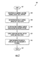
- FIG. 2 is a flow diagram illustrating a method for making the electronic device of FIG. 1 .
- FIGS. 3-10 are a series of schematic cross-sectional diagrams illustrating method steps for making the electronic device of FIG. 1 in greater detail.
- FIG. 11 is a flow diagram which corresponds to the methods steps shown in FIGS. 3-10 .
- the electronic device 30 is a UTBB structure which illustratively includes a substrate 31, a buried oxide layer 32 overlying the substrate, and one or more semiconductor devices 33 overlying the BOX layer.
- the substrate 31 is a silicon substrate, although other suitable substrates (e.g., germanium, SiGe, etc.) may also be used in different embodiments.
- the semiconductor device 33 in the present example is a field effect transistor (FET) including raised source and drain regions 34, 35, and a gate 36.
- FET field effect transistor
- a plurality of semiconductor devices 33 may be formed on a UTBB wafer, which are separated from one another by STI regions 37, as will be discussed further below.
- the raised source and drain regions 34, 35 may be of various types, such as intrinsic silicon, in-situ boron doped SiGe, in-situ phosphorus doped Si/SiC, etc.
- the gate 36 illustratively includes a gate insulating layer 40, which overlies a channel layer 41, and a gate electrode 42 overlying the gate insulating layer.
- a gate contact 43 overlies the gate electrode layer 42.
- a dielectric sidewall spacer 44 is adjacent the gate contact layer 43 as shown.
- Respective source and drain silicide regions 70, 71 and contacts 46, 47 are on the raised source and drain regions 34, 35.
- UTBB devices may otherwise be susceptible to the HF cleaning used in CMOS device manufacturing.
- the STI regions 37 are filled with an insulator 38, such as silicon dioxide (SiO 2 ), which may be recessed during HF cleaning, etc., creating a divot at the interface of the STI regions and the source/drain regions 34, 35. This can cause shorting from the source/drain regions 34, 35 to the substrate 31 .
- silicide regions 70, 71 for the source and drain contacts 46, 47 silicide agglomeration may occur within the divots, which can cause shorting.
- Another potential cause of shorting is overgrowth of epitaxial silicon in the divots from formation of the raised source and drain regions 34, 35.
- Still another potential source of shorting may be an over etch/deposition of source/drain contact material for the contacts 46, 47 that carries over into the divots.
- a crystallized hafnium oxide (HfO 2 ) STI liner is one material that has been used. This material has a strong resistance to many wet etchants, and also is strong enough to block the dry reactive ion etching (RIE) materials during the contact etch process upon annealing.
- RIE dry reactive ion etching
- the conventional approach is to deposit a HfO 2 liner and then simply fill the STI region 37 with an insulator such as SiO 2 . Yet, this process may not be not stable, and it may also be too sensitive to subsequent Chemical Mechanical Polishing/Planarization (CMP) steps.
- CMP Chemical Mechanical Polishing/Planarization
- the method generally includes forming the STI regions 37 by forming a trench 62 (see FIG. 4 ) in the substrate 32 defining a sidewall surface with the substrate and the BOX layer 32, at Block 102 , and lining a bottom portion 50 of the sidewall surface with an oxide layer 53 (e.g., HfO 2 ), at Block 103 .
- an oxide layer 53 e.g., HfO 2
- the method further illustratively includes lining a top portion 52 of the sidewall surface above the bottom portion 50 with a nitride layer 51 (e.g., SiN), at Block 104 , and depositing the insulating material 38 within the nitride and oxide layers, at Block 105.
- the method further includes forming the semiconductor device(s) 33 overlying the BOX layer 32 adjacent the STI regions 37, at Block 106 , which concludes the method illustrated in FIG. 2 (Block 107).
- the substrate 31, BOX layer 32, and ultra thin silicon layer 41 may be provided as a UTBB wafer in some embodiments.
- a pad oxide layer 60 may be formed overlying the silicon layer 41, and an SiN film 61 is deposited on the SiN film, at Block 112 ( FIG. 3 ).
- the SiN film 61 may have a thickness in a range of about 50 to 80 nm
- the pad oxide layer 60 may have a thickness of about 5 nm
- the silicon layer 41 may have a thickness of about 10 nm or less, although other dimensions may be used in different embodiments.
- Lithography may then be performed to define and protect an active (RX) region, so that trenches 62 may be etched for the STI regions 37, at Block 113.
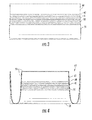
- a HfO 2 liner 53 may then be deposited within the trenches 62 and over the SiN film 61, at Block 114 ( FIG. 4 ).
- the lined trenches 62 are then filled with the insulator 38 (Block 115), e.g., using a High Aspect Ratio Process (HARP) SiO 2 deposition, although other suitable insulators may be used in different embodiments.
- An anneal step is performed, at Block 116, which may be a relatively high temperature anneal (e.g., 1050-1150°C) for HARP SiO 2 .
- a CMP step may be performed to planarize the HARP SiO 2 insulator 38 down to the level of the SiN film 61 ( FIG. 5 ).
- the HARP SiO 2 insulator 38 may then be recessed within the HfO 2 liner 53 down to a level above the ultra thin Si layer 41, at Block 118 ( FIG. 6 ).
- a selective HK etch may then be used (Block 119) to remove any HK from the SiN pad film 61, and also create a small gap 70 inside the STI region 37 adjacent the BOX layer 32, Si layer 41, and pad oxide layer 60, as seen in FIG. 7 .
- the bottom of the gap 70 defines the top or termination point for the bottom portion 50 of the STI region 37.
- the bottom of the gap 70 is between the upper and lower surfaces of the BOX layer 32, and may be around the upper half of the BOX layer, for example.
- a conformal SiN layer 51 may then be deposited to fill the gap 70 resulting from the HK RIE, and to seal the insulating material 38 , at Block 120 ( FIG. 8 ).
- a high temperature iRAD SiN may be deposited, which is very conformal and has very high HF resistivity.
- the open portion of the trench 62 may again be filled with HARP SiO 2 90 and annealed, at Block 121, as described above, and another CMP step may be performed to planarize down to the SiN layer 51, at Block 122 ( FIG. 9 ).
- Deglazing may then be performed to reduce the insulator material 90, at Block 123, and a RIE or WET etch (e.g., hot phosphoric acid) may be used to remove the SiN layer 51, at Block 124 ( FIG. 10 ). If a hot phosphoric acid is used, it may be desirable to control the budget to help avoid excessive SiN etch into the liner region. Further conventional processing steps may then be performed to form the gate 36, raised source/drain regions 34, 35, silicide regions 70, 71, and contacts 46, 47 , and complete the semiconductor device 33 shown in FIG. 1 , at Block 125, which concludes the method illustrated in FIG. 11 (Block 126).
- RIE or WET etch e.g., hot phosphoric acid
- STI consumption by the HF budget is blocked by the SiN liner 51.
- this approach may allow for a relatively large HF budget to be used to form two or more gate stacks. That is, more HF will typically be required for cleaning where two or more gate stacks are used.
- the strong HfO 2 liner 53 advantageously helps prevent source/drain to substrate shorts due to the contact etch process.
Landscapes
- Element Separation (AREA)
- Thin Film Transistor (AREA)
- Chemical & Material Sciences (AREA)
- Crystallography & Structural Chemistry (AREA)
Abstract
Description
- Some embodiments relate to the field of electronic devices and, more particularly, to semiconductor devices and related methods.
- Ultra-thin Body and Buried Oxide (BOX) devices (UTBB) are an attractive device structure in that they may allow for improved semiconductor device scaling. UTBB typically includes an ultra-thin Si body as a channel region, which is fully depleted and is beneficial for short channel effect (SCE) control. Also, with thinner BOX (about 25nm or thinner), compared with ETSOI (extreme thin silicon-on-insulator) devices which have a thicker BOX (more than 50nm), UTBB provides better scaling capability and the ability to tune threshold voltage (Vt) by applying reasonable back bias.
- Shallow trench isolation (STI) regions are typically used in UTBB devices to electrically isolate the semiconductor devices (e.g., field effect transistors (FETs)) from one another. However, with the ultra-thin layers, typical processing operations may cause divots at the interface of the STI regions that can result in shorting from the device source/drain regions to the Si substrate.
- Various approaches have generally been used for enhancing STI isolation structures. One such example is set forth in
U.S. Pat. Pub. No. 2012/0119296 to Anderson et al. , which is directed to trench-generated transistor structures wherein the source and drain of the transistor are defined by doped regions in the semiconductor material of the handle substrate of a semiconductor-on-insulator (SOI) wafer. The gate electrode may be defined from the semiconductor layer of the SOI wafer, which is separated from the handle wafer by an insulating layer. - Despite the existence of such configurations, further enhancements may be desirable for STI regions, particularly where relatively small dimensions are used, such as in UTBB devices.
- In view of the foregoing, it is an aim of some embodiments to provide an electronic device with enhanced interface characteristics between shallow trench isolation (STI) regions and corresponding semiconductor devices.
- According to one aspect, there is provided an electronic device which may include a substrate, a buried oxide (BOX) layer overlying the substrate, at least one semiconductor device overlying the BOX layer, and at least one shallow trench isolation (STI) region in the substrate and adjacent the at least one semiconductor device. The at least one STI region defines a sidewall surface with the substrate and may include an oxide layer lining a bottom portion of the sidewall surface, a nitride layer lining a top portion of the sidewall surface above the bottom portion, and an insulating material within the nitride and oxide layers. Accordingly, the STI regions(s) may advantageously reduce the likelihood of electrical shorting at an interface between the STI region(s) and the corresponding semiconductor device.
- More particularly, the nitride layer may comprise a silicon nitride (SiN) layer, and the oxide layer may comprise a hafnium oxide (HfO2) layer, for example. The nitride layer may extend above the BOX layer, and the oxide layer may terminate below the at least one semiconductor device. Additionally, the insulating material may be different than the nitride and oxide layers. By way of example, the insulating material may comprise silicon dioxide (SiO2).
- The at least one semiconductor device may comprise at least one field effect transistor (FET), for example. More particularly, the at least one FET may comprise raised source and drain regions and a channel region therebetween. Furthermore, the at least one STI region may comprise a plurality of STI regions on opposing sides of the at least one semiconductor device.
- A method for making an electronic device may include forming at least one STI region in a substrate having a BOX layer overlying the substrate. This may be done by at least forming a trench in the substrate defining a sidewall surface with the substrate, lining a bottom portion of the sidewall surface with an oxide layer, lining a top portion of the sidewall surface above the bottom portion with a nitride layer, and depositing an insulating material within the nitride and oxide layers. The method may further include forming at least one semiconductor device overlying the BOX layer adjacent the at least one STI region.
- An electronic device may comprise a substrate; a buried oxide (BOX) layer overlying said substrate; at least one semiconductor device overlying said BOX layer; and at least one shallow trench isolation (STI) region in the substrate and adjacent the at least one semiconductor device, said at least one STI region defining a sidewall surface with the substrate and comprising an oxide layer lining a bottom portion of the sidewall surface, a nitride layer lining a top portion of the sidewall surface above the bottom portion, and an insulating material within the nitride and oxide layers.
- The nitride layer may comprise a silicon nitride (SiN) layer.
- The oxide layer may comprise a hafnium oxide (HfO2) layer.
- The nitride layer may extend above said BOX layer.
- The said oxide layer may terminate below said at least one semiconductor device.
- The said insulating material may be different than the nitride and oxide layers.
- The said insulating material may comprise silicon dioxide (SiO2).
- The said at least one semiconductor device may comprise at least one field effect transistor (FET).
- The said at FET may comprise raised source and drain regions and a channel region therebetween.
- The said at least one STI region may comprise a plurality of STI regions on opposing sides of said at least one semiconductor device.
- An electronic device may comprise a substrate; a buried oxide (BOX) layer overlying said substrate; at least one semiconductor device overlying said BOX layer; and at least one shallow trench isolation (STI) region in the substrate and adjacent the at least one semiconductor device, said at least one STI region defining a sidewall surface with said substrate and comprising a hafnium oxide (HfO2) layer lining a bottom portion of the sidewall surface, a silicon nitride (SiN) layer lining a top portion of the sidewall surface above the bottom portion, and an insulating material within the SiN and HfO2 layers.
- The said SiN layer may extend above said BOX layer.
- The said HfO2 layer may terminate below said at least one semiconductor device.
- The said insulating material may be different than the nitride and oxide layers.
- A method for making an electronic device may comprise forming at least one shallow trench isolation (STI) region in a substrate having a buried oxide (BOX) layer overlying the substrate by at least forming a trench in the substrate defining a sidewall surface with the substrate, lining a bottom portion of the sidewall surface with an oxide layer, lining a top portion of the sidewall surface above the bottom portion with a nitride layer, and depositing an insulating material within the nitride and oxide layers; and forming at least one semiconductor device overlying the BOX layer adjacent the at least one STI region.
- Lining the bottom portion of the sidewall surface may further comprise lining the trench with the oxide layer; and etching away the oxide layer down to the bottom portion.
- The nitride layer may comprise a silicon nitride (SiN) layer.
- The oxide layer may comprise a hafnium oxide (HfO2) layer.
- The nitride layer may extend above the BOX layer.
- The oxide layer may terminate below the at least one semiconductor device.
- The insulating material may be different than the nitride and oxide layers.
- The insulating material may comprise silicon dioxide (SiO2).
-
FIG. 1 is a schematic cross-sectional diagram of an electronic device in accordance with an embodiment including enhanced STI regions. -
FIG. 2 is a flow diagram illustrating a method for making the electronic device ofFIG. 1 . -
FIGS. 3-10 are a series of schematic cross-sectional diagrams illustrating method steps for making the electronic device ofFIG. 1 in greater detail. -
FIG. 11 is a flow diagram which corresponds to the methods steps shown inFIGS. 3-10 . - Some embodiments will now be described more fully hereinafter with reference to the accompanying drawings, in which preferred embodiments are shown. This invention may, however, be embodied in many different forms and should not be construed as limited to the embodiments set forth herein. Rather, these embodiments are provided so that this disclosure will be thorough and complete, and will fully convey the scope of the invention to those skilled in the art. Like numbers refer to like elements throughout.
- Referring initially to
FIG. 1 , anelectronic device 30 is first described. In the illustrated example, theelectronic device 30 is a UTBB structure which illustratively includes asubstrate 31, a buriedoxide layer 32 overlying the substrate, and one ormore semiconductor devices 33 overlying the BOX layer. In the illustrated example, thesubstrate 31 is a silicon substrate, although other suitable substrates (e.g., germanium, SiGe, etc.) may also be used in different embodiments. Also, thesemiconductor device 33 in the present example is a field effect transistor (FET) including raised source anddrain regions gate 36. In a typical implementation, a plurality of semiconductor devices 33 (e.g., FETs) may be formed on a UTBB wafer, which are separated from one another bySTI regions 37, as will be discussed further below. The raised source and drainregions - The
gate 36 illustratively includes agate insulating layer 40, which overlies achannel layer 41, and agate electrode 42 overlying the gate insulating layer. Agate contact 43 overlies thegate electrode layer 42. Adielectric sidewall spacer 44 is adjacent thegate contact layer 43 as shown. Respective source and drainsilicide regions contacts regions - By way of background, due to the relatively
thin BOX layer 32, UTBB devices may otherwise be susceptible to the HF cleaning used in CMOS device manufacturing. More particularly, theSTI regions 37 are filled with aninsulator 38, such as silicon dioxide (SiO2), which may be recessed during HF cleaning, etc., creating a divot at the interface of the STI regions and the source/drain regions drain regions substrate 31. For example, when depositing thesilicide regions drain contacts regions contacts - One technique that has been attempted to reduce this type of shorting is to form a robust STI liner. A crystallized hafnium oxide (HfO2) STI liner is one material that has been used. This material has a strong resistance to many wet etchants, and also is strong enough to block the dry reactive ion etching (RIE) materials during the contact etch process upon annealing. However, the conventional approach is to deposit a HfO2 liner and then simply fill the
STI region 37 with an insulator such as SiO2. Yet, this process may not be not stable, and it may also be too sensitive to subsequent Chemical Mechanical Polishing/Planarization (CMP) steps. - Referring additionally to
FIG. 2 , an example approach form making the UTBBelectronic device 30 is first described. With reference to the flow diagram 100, beginning atBlock 101, the method generally includes forming theSTI regions 37 by forming a trench 62 (seeFIG. 4 ) in thesubstrate 32 defining a sidewall surface with the substrate and theBOX layer 32, atBlock 102, and lining abottom portion 50 of the sidewall surface with an oxide layer 53 (e.g., HfO2), atBlock 103. The method further illustratively includes lining atop portion 52 of the sidewall surface above thebottom portion 50 with a nitride layer 51 (e.g., SiN), atBlock 104, and depositing the insulatingmaterial 38 within the nitride and oxide layers, atBlock 105. The method further includes forming the semiconductor device(s) 33 overlying theBOX layer 32 adjacent theSTI regions 37, atBlock 106, which concludes the method illustrated inFIG. 2 (Block 107). - The fabrication process for the
electronic device 30 will now be described in further detail with reference toFIGS. 3-8 and the flow diagram 110 ofFIG. 11 . Beginning atBlock 111, thesubstrate 31,BOX layer 32, and ultra thin silicon layer 41 (which is later patterned to provide the channel) may be provided as a UTBB wafer in some embodiments. Apad oxide layer 60 may be formed overlying thesilicon layer 41, and anSiN film 61 is deposited on the SiN film, at Block 112 (FIG. 3 ). By way of example, theSiN film 61 may have a thickness in a range of about 50 to 80 nm, thepad oxide layer 60 may have a thickness of about 5 nm, and thesilicon layer 41 may have a thickness of about 10 nm or less, although other dimensions may be used in different embodiments. - Lithography may then be performed to define and protect an active (RX) region, so that
trenches 62 may be etched for theSTI regions 37, atBlock 113. A HfO2 liner 53 may then be deposited within thetrenches 62 and over theSiN film 61, at Block 114 (FIG. 4 ). The linedtrenches 62 are then filled with the insulator 38 (Block 115), e.g., using a High Aspect Ratio Process (HARP) SiO2 deposition, although other suitable insulators may be used in different embodiments. An anneal step is performed, atBlock 116, which may be a relatively high temperature anneal (e.g., 1050-1150°C) for HARP SiO2. AtBlock 117, a CMP step may be performed to planarize the HARP SiO2 insulator 38 down to the level of the SiN film 61 (FIG. 5 ). - The HARP SiO2 insulator 38 may then be recessed within the HfO2 liner 53 down to a level above the ultra
thin Si layer 41, at Block 118 (FIG. 6 ). A selective HK etch may then be used (Block 119) to remove any HK from theSiN pad film 61, and also create asmall gap 70 inside theSTI region 37 adjacent theBOX layer 32,Si layer 41, andpad oxide layer 60, as seen inFIG. 7 . The bottom of thegap 70 defines the top or termination point for thebottom portion 50 of theSTI region 37. In the illustrated example, the bottom of thegap 70 is between the upper and lower surfaces of theBOX layer 32, and may be around the upper half of the BOX layer, for example. - A
conformal SiN layer 51 may then be deposited to fill thegap 70 resulting from the HK RIE, and to seal the insulatingmaterial 38, at Block 120 (FIG. 8 ). By way of example, a high temperature iRAD SiN may be deposited, which is very conformal and has very high HF resistivity. The open portion of thetrench 62 may again be filled withHARP SiO 2 90 and annealed, atBlock 121, as described above, and another CMP step may be performed to planarize down to theSiN layer 51, at Block 122 (FIG. 9 ). Deglazing may then be performed to reduce theinsulator material 90, atBlock 123, and a RIE or WET etch (e.g., hot phosphoric acid) may be used to remove theSiN layer 51, at Block 124 (FIG. 10 ). If a hot phosphoric acid is used, it may be desirable to control the budget to help avoid excessive SiN etch into the liner region. Further conventional processing steps may then be performed to form thegate 36, raised source/drain regions silicide regions contacts semiconductor device 33 shown inFIG. 1 , atBlock 125, which concludes the method illustrated inFIG. 11 (Block 126). - It will therefore be appreciated that as a result of the above-described process, STI consumption by the HF budget is blocked by the
SiN liner 51. As such, this approach may allow for a relatively large HF budget to be used to form two or more gate stacks. That is, more HF will typically be required for cleaning where two or more gate stacks are used. Moreover, the strong HfO2 liner 53 advantageously helps prevent source/drain to substrate shorts due to the contact etch process. - Many modifications and other embodiments of the invention will come to the mind of one skilled in the art having the benefit of the teachings presented in the foregoing descriptions and the associated drawings. Therefore, it is understood that the invention is not to be limited to the specific embodiments disclosed, and that modifications and embodiments are intended to be included within the scope of the appended claims.
Claims (15)
- An electronic device comprising:a substrate;a buried oxide (BOX) layer overlying said substrate;at least one semiconductor device overlying said BOX layer; andat least one shallow trench isolation (STI) region in the substrate and adjacent the at least one semiconductor device, said at least one STI region defining a sidewall surface with the substrate and comprising
an oxide layer lining a bottom portion of the sidewall surface,
a nitride layer lining a top portion of the sidewall surface above the bottom portion, and
an insulating material within the nitride and oxide layers. - The electronic device of Claim 1 wherein the nitride layer comprises a silicon nitride (SiN) layer,
- The electronic device of Claim 1 or 2 wherein the oxide layer comprises a hafnium oxide (HfO2) layer.
- The electronic device of Claim 1, 2 or 3 wherein said nitride layer extends above said BOX layer.
- The electronic device of any preceding Claim wherein said at least one semiconductor device comprises at least one field effect transistor (FET).
- The electronic device of Claim 5 wherein said at FET comprises raised source and drain regions and a channel region therebetween.
- The electronic device of any preceding Claim wherein said at least one STI region comprises a plurality of STI regions on opposing sides of said at least one semiconductor device.
- A method for making an electronic device comprising:forming at least one shallow trench isolation (STI) region in a substrate having a buried oxide (BOX) layer overlying the substrate by at least
forming a trench in the substrate defining a sidewall surface with the substrate,
lining a bottom portion of the sidewall surface with an oxide layer,
lining a top portion of the sidewall surface above the bottom portion with a nitride layer, and
depositing an insulating material within the nitride and oxide layers; andforming at least one semiconductor device overlying the BOX layer adjacent the at least one STI region. - The method of Claim 8 wherein lining the bottom portion of the sidewall surface further comprises:lining the trench with the oxide layer; andetching away the oxide layer down to the bottom portion.
- The method of Claim 8 or 9 wherein the nitride layer comprises a silicon nitride (SiN) layer.
- The method of Claim 8, 9 or 10 wherein the oxide layer comprises a hafnium oxide (HfO2) layer.
- The method of any Claims 8 to 11 wherein the nitride layer extends above the BOX layer.
- The method or device of any preceding Claim wherein the oxide layer terminates below the at least one semiconductor device.
- The method or device of any preceding Claim wherein the insulating material is different than the nitride and oxide layers.
- The method or device of any preceding Claim wherein the insulating material comprises silicon dioxide (SiO2).
Applications Claiming Priority (1)
| Application Number | Priority Date | Filing Date | Title |
|---|---|---|---|
| US13/590,836 US9768055B2 (en) | 2012-08-21 | 2012-08-21 | Isolation regions for SOI devices |
Publications (3)
| Publication Number | Publication Date |
|---|---|
| EP2701187A2 true EP2701187A2 (en) | 2014-02-26 |
| EP2701187A3 EP2701187A3 (en) | 2014-04-23 |
| EP2701187B1 EP2701187B1 (en) | 2016-10-26 |
Family
ID=48918295
Family Applications (1)
| Application Number | Title | Priority Date | Filing Date |
|---|---|---|---|
| EP13179641.9A Active EP2701187B1 (en) | 2012-08-21 | 2013-08-07 | Electronic Device including Shallow Trench Isolation (STI) Regions with Bottom Oxide Linear and Upper Nitride Liner and Related Methods |
Country Status (4)
| Country | Link |
|---|---|
| US (1) | US9768055B2 (en) |
| EP (1) | EP2701187B1 (en) |
| JP (1) | JP2014042022A (en) |
| CN (2) | CN103633084A (en) |
Cited By (2)
| Publication number | Priority date | Publication date | Assignee | Title |
|---|---|---|---|---|
| EP3131119A1 (en) * | 2015-08-10 | 2017-02-15 | Renesas Electronics Corporation | Soi semiconductor device and manufacturing method of the same |
| US9633857B1 (en) | 2016-03-31 | 2017-04-25 | Globalfoundries Inc. | Semiconductor structure including a trench capping layer and method for the formation thereof |
Families Citing this family (8)
| Publication number | Priority date | Publication date | Assignee | Title |
|---|---|---|---|---|
| JP5888064B2 (en) | 2012-03-29 | 2016-03-16 | 富士通株式会社 | Compound semiconductor device and manufacturing method thereof |
| US9768055B2 (en) * | 2012-08-21 | 2017-09-19 | Stmicroelectronics, Inc. | Isolation regions for SOI devices |
| US8987070B2 (en) * | 2012-09-12 | 2015-03-24 | International Business Machines Corporation | SOI device with embedded liner in box layer to limit STI recess |
| US9136330B2 (en) * | 2013-07-22 | 2015-09-15 | GlobalFoundries, Inc. | Shallow trench isolation |
| US10204982B2 (en) * | 2013-10-08 | 2019-02-12 | Stmicroelectronics, Inc. | Semiconductor device with relaxation reduction liner and associated methods |
| DE102016117030B4 (en) * | 2016-07-17 | 2018-07-05 | X-Fab Semiconductor Foundries Ag | Production of Semiconductor Structures on a Carrier Substrate Transferable by Transfer Print. |
| US10153195B1 (en) | 2017-05-18 | 2018-12-11 | Micron Technology, Inc. | Semiconductor constructions comprising dielectric material |
| CN108493202B (en) * | 2018-02-01 | 2020-10-27 | 北京大学 | A UTBB photodetector element and device suitable for submicron pixels |
Citations (1)
| Publication number | Priority date | Publication date | Assignee | Title |
|---|---|---|---|---|
| US20120119296A1 (en) | 2009-09-18 | 2012-05-17 | International Business Machines Corporation | Trench-generated transistor structures, device structures, and design structures |
Family Cites Families (24)
| Publication number | Priority date | Publication date | Assignee | Title |
|---|---|---|---|---|
| US6657276B1 (en) * | 2001-12-10 | 2003-12-02 | Advanced Micro Devices, Inc. | Shallow trench isolation (STI) region with high-K liner and method of formation |
| US6689665B1 (en) | 2002-10-11 | 2004-02-10 | Taiwan Semiconductor Manufacturing, Co., Ltd | Method of forming an STI feature while avoiding or reducing divot formation |
| KR100532503B1 (en) | 2004-02-03 | 2005-11-30 | 삼성전자주식회사 | Method for forming shallow trench isolation |
| KR100568259B1 (en) * | 2004-12-14 | 2006-04-07 | 삼성전자주식회사 | Trench isolation semiconductor device and method of forming the same |
| JP2006269789A (en) | 2005-03-24 | 2006-10-05 | Toshiba Corp | Semiconductor device and manufacturing method thereof |
| US7384849B2 (en) * | 2005-03-25 | 2008-06-10 | Micron Technology, Inc. | Methods of forming recessed access devices associated with semiconductor constructions |
| US7586158B2 (en) * | 2005-07-07 | 2009-09-08 | Infineon Technologies Ag | Piezoelectric stress liner for bulk and SOI |
| US20070132056A1 (en) | 2005-12-09 | 2007-06-14 | Advanced Analogic Technologies, Inc. | Isolation structures for semiconductor integrated circuit substrates and methods of forming the same |
| US7514336B2 (en) | 2005-12-29 | 2009-04-07 | Agere Systems Inc. | Robust shallow trench isolation structures and a method for forming shallow trench isolation structures |
| US20070259500A1 (en) | 2006-05-05 | 2007-11-08 | International Business Machines Corporation | Structure Having Isolation Structure Including Deuterium Within A Substrate And Related Method |
| KR100772109B1 (en) | 2006-06-30 | 2007-11-01 | 주식회사 하이닉스반도체 | Device Separating Method of Semiconductor Device |
| US20080217686A1 (en) * | 2007-03-09 | 2008-09-11 | International Business Machines Corporation | Ultra-thin soi cmos with raised epitaxial source and drain and embedded sige pfet extension |
| US8237229B2 (en) | 2008-05-22 | 2012-08-07 | Stmicroelectronics Inc. | Method and apparatus for buried-channel semiconductor device |
| US8163625B2 (en) | 2009-04-07 | 2012-04-24 | Taiwan Semiconductor Manufacturing Company, Ltd. | Method for fabricating an isolation structure |
| US8106456B2 (en) * | 2009-07-29 | 2012-01-31 | International Business Machines Corporation | SOI transistors having an embedded extension region to improve extension resistance and channel strain characteristics |
| KR101062849B1 (en) * | 2009-10-30 | 2011-09-07 | 주식회사 하이닉스반도체 | Semiconductor device and manufacturing method thereof |
| US8450834B2 (en) | 2010-02-16 | 2013-05-28 | Taiwan Semiconductor Manufacturing Company, Ltd. | Spacer structure of a field effect transistor with an oxygen-containing layer between two oxygen-sealing layers |
| US8187975B1 (en) | 2010-12-06 | 2012-05-29 | Stmicroelectronics, Inc. | Hydrochloric acid etch and low temperature epitaxy in a single chamber for raised source-drain fabrication |
| US8900973B2 (en) | 2011-08-30 | 2014-12-02 | International Business Machines Corporation | Method to enable compressively strained pFET channel in a FinFET structure by implant and thermal diffusion |
| US8703550B2 (en) | 2012-06-18 | 2014-04-22 | International Business Machines Corporation | Dual shallow trench isolation liner for preventing electrical shorts |
| US20130334561A1 (en) | 2012-06-19 | 2013-12-19 | Hsiu-Jen Lin | Method for bonding led wafer, method for manufacturing led chip and bonding structure |
| US8673738B2 (en) | 2012-06-25 | 2014-03-18 | International Business Machines Corporation | Shallow trench isolation structures |
| US9768055B2 (en) * | 2012-08-21 | 2017-09-19 | Stmicroelectronics, Inc. | Isolation regions for SOI devices |
| US9000555B2 (en) | 2012-08-21 | 2015-04-07 | Stmicroelectronics, Inc. | Electronic device including shallow trench isolation (STI) regions with bottom nitride liner and upper oxide liner and related methods |
-
2012
- 2012-08-21 US US13/590,836 patent/US9768055B2/en active Active
-
2013
- 2013-08-02 CN CN201310337452.4A patent/CN103633084A/en active Pending
- 2013-08-02 CN CN201320477988.1U patent/CN203690303U/en not_active Expired - Fee Related
- 2013-08-07 EP EP13179641.9A patent/EP2701187B1/en active Active
- 2013-08-08 JP JP2013165436A patent/JP2014042022A/en active Pending
Patent Citations (1)
| Publication number | Priority date | Publication date | Assignee | Title |
|---|---|---|---|---|
| US20120119296A1 (en) | 2009-09-18 | 2012-05-17 | International Business Machines Corporation | Trench-generated transistor structures, device structures, and design structures |
Cited By (3)
| Publication number | Priority date | Publication date | Assignee | Title |
|---|---|---|---|---|
| EP3131119A1 (en) * | 2015-08-10 | 2017-02-15 | Renesas Electronics Corporation | Soi semiconductor device and manufacturing method of the same |
| US9633857B1 (en) | 2016-03-31 | 2017-04-25 | Globalfoundries Inc. | Semiconductor structure including a trench capping layer and method for the formation thereof |
| US10103224B2 (en) | 2016-03-31 | 2018-10-16 | Globalfoundries Inc. | Semiconductor structure including a trench capping layer |
Also Published As
| Publication number | Publication date |
|---|---|
| EP2701187A3 (en) | 2014-04-23 |
| EP2701187B1 (en) | 2016-10-26 |
| US20140054699A1 (en) | 2014-02-27 |
| CN203690303U (en) | 2014-07-02 |
| CN103633084A (en) | 2014-03-12 |
| US9768055B2 (en) | 2017-09-19 |
| JP2014042022A (en) | 2014-03-06 |
Similar Documents
| Publication | Publication Date | Title |
|---|---|---|
| EP2701187B1 (en) | Electronic Device including Shallow Trench Isolation (STI) Regions with Bottom Oxide Linear and Upper Nitride Liner and Related Methods | |
| US9000555B2 (en) | Electronic device including shallow trench isolation (STI) regions with bottom nitride liner and upper oxide liner and related methods | |
| TWI624876B (en) | FINFET with notched fins and method of forming same | |
| CN102598244B (en) | Hybrid double box back gate silicon-on-insulator wafers with enhanced mobility channels | |
| US8383464B2 (en) | Method for producing field effect transistors with a back gate and semiconductor device | |
| US8106456B2 (en) | SOI transistors having an embedded extension region to improve extension resistance and channel strain characteristics | |
| US7790528B2 (en) | Dual substrate orientation or bulk on SOI integrations using oxidation for silicon epitaxy spacer formation | |
| US7749829B2 (en) | Step height reduction between SOI and EPI for DSO and BOS integration | |
| US20120104495A1 (en) | Semiconductor structure and method for manufacturing the same | |
| US8962430B2 (en) | Method for the formation of a protective dual liner for a shallow trench isolation structure | |
| US20120261792A1 (en) | Soi device with dti and sti | |
| US9595578B2 (en) | Undercut insulating regions for silicon-on-insulator device | |
| CN102376769A (en) | Ultra-thin body transistor and manufacturing method thereof | |
| CN104103516B (en) | Fleet plough groove isolation structure and forming method thereof | |
| US20150093861A1 (en) | Method for the formation of cmos transistors | |
| JP2008533705A (en) | Fabrication of carrier substrate contacts to trench-isolated SOI integrated circuits with high voltage components | |
| US8987070B2 (en) | SOI device with embedded liner in box layer to limit STI recess | |
| CN103515283A (en) | Semiconductor device manufacturing method | |
| CN102468215A (en) | Trench isolation structure and forming method thereof | |
| US12476134B2 (en) | Semiconductor structure for digital and radiofrequency applications, and method for manufacturing such a structure | |
| US7217604B2 (en) | Structure and method for thin box SOI device | |
| CN102903663A (en) | Semiconductor devices having encapsulated isolation regions and related fabrication methods |
Legal Events
| Date | Code | Title | Description |
|---|---|---|---|
| PUAI | Public reference made under article 153(3) epc to a published international application that has entered the european phase |
Free format text: ORIGINAL CODE: 0009012 |
|
| AK | Designated contracting states |
Kind code of ref document: A2 Designated state(s): AL AT BE BG CH CY CZ DE DK EE ES FI FR GB GR HR HU IE IS IT LI LT LU LV MC MK MT NL NO PL PT RO RS SE SI SK SM TR |
|
| AX | Request for extension of the european patent |
Extension state: BA ME |
|
| PUAL | Search report despatched |
Free format text: ORIGINAL CODE: 0009013 |
|
| AK | Designated contracting states |
Kind code of ref document: A3 Designated state(s): AL AT BE BG CH CY CZ DE DK EE ES FI FR GB GR HR HU IE IS IT LI LT LU LV MC MK MT NL NO PL PT RO RS SE SI SK SM TR |
|
| AX | Request for extension of the european patent |
Extension state: BA ME |
|
| RIC1 | Information provided on ipc code assigned before grant |
Ipc: H01L 21/762 20060101AFI20140318BHEP |
|
| 17P | Request for examination filed |
Effective date: 20141015 |
|
| RBV | Designated contracting states (corrected) |
Designated state(s): AL AT BE BG CH CY CZ DE DK EE ES FI FR GB GR HR HU IE IS IT LI LT LU LV MC MK MT NL NO PL PT RO RS SE SI SK SM TR |
|
| REG | Reference to a national code |
Ref country code: DE Ref legal event code: R079 Ref document number: 602013013148 Country of ref document: DE Free format text: PREVIOUS MAIN CLASS: H01L0021762000 Ipc: H01L0029786000 |
|
| RIC1 | Information provided on ipc code assigned before grant |
Ipc: H01L 29/786 20060101AFI20160205BHEP Ipc: H01L 21/762 20060101ALI20160205BHEP Ipc: H01L 29/66 20060101ALI20160205BHEP |
|
| GRAP | Despatch of communication of intention to grant a patent |
Free format text: ORIGINAL CODE: EPIDOSNIGR1 |
|
| INTG | Intention to grant announced |
Effective date: 20160321 |
|
| GRAS | Grant fee paid |
Free format text: ORIGINAL CODE: EPIDOSNIGR3 |
|
| GRAA | (expected) grant |
Free format text: ORIGINAL CODE: 0009210 |
|
| AK | Designated contracting states |
Kind code of ref document: B1 Designated state(s): AL AT BE BG CH CY CZ DE DK EE ES FI FR GB GR HR HU IE IS IT LI LT LU LV MC MK MT NL NO PL PT RO RS SE SI SK SM TR |
|
| REG | Reference to a national code |
Ref country code: GB Ref legal event code: FG4D |
|
| REG | Reference to a national code |
Ref country code: CH Ref legal event code: EP |
|
| REG | Reference to a national code |
Ref country code: AT Ref legal event code: REF Ref document number: 840568 Country of ref document: AT Kind code of ref document: T Effective date: 20161115 |
|
| REG | Reference to a national code |
Ref country code: IE Ref legal event code: FG4D |
|
| REG | Reference to a national code |
Ref country code: DE Ref legal event code: R096 Ref document number: 602013013148 Country of ref document: DE |
|
| REG | Reference to a national code |
Ref country code: LT Ref legal event code: MG4D |
|
| PG25 | Lapsed in a contracting state [announced via postgrant information from national office to epo] |
Ref country code: LV Free format text: LAPSE BECAUSE OF FAILURE TO SUBMIT A TRANSLATION OF THE DESCRIPTION OR TO PAY THE FEE WITHIN THE PRESCRIBED TIME-LIMIT Effective date: 20161026 |
|
| REG | Reference to a national code |
Ref country code: NL Ref legal event code: MP Effective date: 20161026 |
|
| REG | Reference to a national code |
Ref country code: AT Ref legal event code: MK05 Ref document number: 840568 Country of ref document: AT Kind code of ref document: T Effective date: 20161026 |
|
| PG25 | Lapsed in a contracting state [announced via postgrant information from national office to epo] |
Ref country code: GR Free format text: LAPSE BECAUSE OF FAILURE TO SUBMIT A TRANSLATION OF THE DESCRIPTION OR TO PAY THE FEE WITHIN THE PRESCRIBED TIME-LIMIT Effective date: 20170127 Ref country code: NO Free format text: LAPSE BECAUSE OF FAILURE TO SUBMIT A TRANSLATION OF THE DESCRIPTION OR TO PAY THE FEE WITHIN THE PRESCRIBED TIME-LIMIT Effective date: 20170126 Ref country code: SE Free format text: LAPSE BECAUSE OF FAILURE TO SUBMIT A TRANSLATION OF THE DESCRIPTION OR TO PAY THE FEE WITHIN THE PRESCRIBED TIME-LIMIT Effective date: 20161026 Ref country code: LT Free format text: LAPSE BECAUSE OF FAILURE TO SUBMIT A TRANSLATION OF THE DESCRIPTION OR TO PAY THE FEE WITHIN THE PRESCRIBED TIME-LIMIT Effective date: 20161026 |
|
| PG25 | Lapsed in a contracting state [announced via postgrant information from national office to epo] |
Ref country code: ES Free format text: LAPSE BECAUSE OF FAILURE TO SUBMIT A TRANSLATION OF THE DESCRIPTION OR TO PAY THE FEE WITHIN THE PRESCRIBED TIME-LIMIT Effective date: 20161026 Ref country code: RS Free format text: LAPSE BECAUSE OF FAILURE TO SUBMIT A TRANSLATION OF THE DESCRIPTION OR TO PAY THE FEE WITHIN THE PRESCRIBED TIME-LIMIT Effective date: 20161026 Ref country code: HR Free format text: LAPSE BECAUSE OF FAILURE TO SUBMIT A TRANSLATION OF THE DESCRIPTION OR TO PAY THE FEE WITHIN THE PRESCRIBED TIME-LIMIT Effective date: 20161026 Ref country code: PT Free format text: LAPSE BECAUSE OF FAILURE TO SUBMIT A TRANSLATION OF THE DESCRIPTION OR TO PAY THE FEE WITHIN THE PRESCRIBED TIME-LIMIT Effective date: 20170227 Ref country code: IS Free format text: LAPSE BECAUSE OF FAILURE TO SUBMIT A TRANSLATION OF THE DESCRIPTION OR TO PAY THE FEE WITHIN THE PRESCRIBED TIME-LIMIT Effective date: 20170226 Ref country code: FI Free format text: LAPSE BECAUSE OF FAILURE TO SUBMIT A TRANSLATION OF THE DESCRIPTION OR TO PAY THE FEE WITHIN THE PRESCRIBED TIME-LIMIT Effective date: 20161026 Ref country code: NL Free format text: LAPSE BECAUSE OF FAILURE TO SUBMIT A TRANSLATION OF THE DESCRIPTION OR TO PAY THE FEE WITHIN THE PRESCRIBED TIME-LIMIT Effective date: 20161026 Ref country code: BE Free format text: LAPSE BECAUSE OF FAILURE TO SUBMIT A TRANSLATION OF THE DESCRIPTION OR TO PAY THE FEE WITHIN THE PRESCRIBED TIME-LIMIT Effective date: 20161026 Ref country code: PL Free format text: LAPSE BECAUSE OF FAILURE TO SUBMIT A TRANSLATION OF THE DESCRIPTION OR TO PAY THE FEE WITHIN THE PRESCRIBED TIME-LIMIT Effective date: 20161026 Ref country code: AT Free format text: LAPSE BECAUSE OF FAILURE TO SUBMIT A TRANSLATION OF THE DESCRIPTION OR TO PAY THE FEE WITHIN THE PRESCRIBED TIME-LIMIT Effective date: 20161026 |
|
| REG | Reference to a national code |
Ref country code: DE Ref legal event code: R097 Ref document number: 602013013148 Country of ref document: DE |
|
| PG25 | Lapsed in a contracting state [announced via postgrant information from national office to epo] |
Ref country code: EE Free format text: LAPSE BECAUSE OF FAILURE TO SUBMIT A TRANSLATION OF THE DESCRIPTION OR TO PAY THE FEE WITHIN THE PRESCRIBED TIME-LIMIT Effective date: 20161026 Ref country code: DK Free format text: LAPSE BECAUSE OF FAILURE TO SUBMIT A TRANSLATION OF THE DESCRIPTION OR TO PAY THE FEE WITHIN THE PRESCRIBED TIME-LIMIT Effective date: 20161026 Ref country code: SK Free format text: LAPSE BECAUSE OF FAILURE TO SUBMIT A TRANSLATION OF THE DESCRIPTION OR TO PAY THE FEE WITHIN THE PRESCRIBED TIME-LIMIT Effective date: 20161026 Ref country code: RO Free format text: LAPSE BECAUSE OF FAILURE TO SUBMIT A TRANSLATION OF THE DESCRIPTION OR TO PAY THE FEE WITHIN THE PRESCRIBED TIME-LIMIT Effective date: 20161026 Ref country code: CZ Free format text: LAPSE BECAUSE OF FAILURE TO SUBMIT A TRANSLATION OF THE DESCRIPTION OR TO PAY THE FEE WITHIN THE PRESCRIBED TIME-LIMIT Effective date: 20161026 |
|
| PG25 | Lapsed in a contracting state [announced via postgrant information from national office to epo] |
Ref country code: IT Free format text: LAPSE BECAUSE OF FAILURE TO SUBMIT A TRANSLATION OF THE DESCRIPTION OR TO PAY THE FEE WITHIN THE PRESCRIBED TIME-LIMIT Effective date: 20161026 Ref country code: SM Free format text: LAPSE BECAUSE OF FAILURE TO SUBMIT A TRANSLATION OF THE DESCRIPTION OR TO PAY THE FEE WITHIN THE PRESCRIBED TIME-LIMIT Effective date: 20161026 Ref country code: BG Free format text: LAPSE BECAUSE OF FAILURE TO SUBMIT A TRANSLATION OF THE DESCRIPTION OR TO PAY THE FEE WITHIN THE PRESCRIBED TIME-LIMIT Effective date: 20170126 |
|
| PLBE | No opposition filed within time limit |
Free format text: ORIGINAL CODE: 0009261 |
|
| STAA | Information on the status of an ep patent application or granted ep patent |
Free format text: STATUS: NO OPPOSITION FILED WITHIN TIME LIMIT |
|
| 26N | No opposition filed |
Effective date: 20170727 |
|
| REG | Reference to a national code |
Ref country code: FR Ref legal event code: PLFP Year of fee payment: 5 |
|
| PG25 | Lapsed in a contracting state [announced via postgrant information from national office to epo] |
Ref country code: SI Free format text: LAPSE BECAUSE OF FAILURE TO SUBMIT A TRANSLATION OF THE DESCRIPTION OR TO PAY THE FEE WITHIN THE PRESCRIBED TIME-LIMIT Effective date: 20161026 |
|
| REG | Reference to a national code |
Ref country code: CH Ref legal event code: PL |
|
| PG25 | Lapsed in a contracting state [announced via postgrant information from national office to epo] |
Ref country code: MC Free format text: LAPSE BECAUSE OF FAILURE TO SUBMIT A TRANSLATION OF THE DESCRIPTION OR TO PAY THE FEE WITHIN THE PRESCRIBED TIME-LIMIT Effective date: 20161026 |
|
| GBPC | Gb: european patent ceased through non-payment of renewal fee |
Effective date: 20170807 |
|
| PG25 | Lapsed in a contracting state [announced via postgrant information from national office to epo] |
Ref country code: LI Free format text: LAPSE BECAUSE OF NON-PAYMENT OF DUE FEES Effective date: 20170831 Ref country code: CH Free format text: LAPSE BECAUSE OF NON-PAYMENT OF DUE FEES Effective date: 20170831 |
|
| REG | Reference to a national code |
Ref country code: IE Ref legal event code: MM4A |
|
| PG25 | Lapsed in a contracting state [announced via postgrant information from national office to epo] |
Ref country code: LU Free format text: LAPSE BECAUSE OF NON-PAYMENT OF DUE FEES Effective date: 20170807 |
|
| REG | Reference to a national code |
Ref country code: FR Ref legal event code: PLFP Year of fee payment: 6 |
|
| PG25 | Lapsed in a contracting state [announced via postgrant information from national office to epo] |
Ref country code: GB Free format text: LAPSE BECAUSE OF NON-PAYMENT OF DUE FEES Effective date: 20170807 Ref country code: IE Free format text: LAPSE BECAUSE OF NON-PAYMENT OF DUE FEES Effective date: 20170807 |
|
| PG25 | Lapsed in a contracting state [announced via postgrant information from national office to epo] |
Ref country code: MT Free format text: LAPSE BECAUSE OF NON-PAYMENT OF DUE FEES Effective date: 20170807 |
|
| REG | Reference to a national code |
Ref country code: DE Ref legal event code: R082 Ref document number: 602013013148 Country of ref document: DE Representative=s name: PAGE, WHITE & FARRER GERMANY LLP, DE |
|
| PG25 | Lapsed in a contracting state [announced via postgrant information from national office to epo] |
Ref country code: HU Free format text: LAPSE BECAUSE OF FAILURE TO SUBMIT A TRANSLATION OF THE DESCRIPTION OR TO PAY THE FEE WITHIN THE PRESCRIBED TIME-LIMIT; INVALID AB INITIO Effective date: 20130807 |
|
| PG25 | Lapsed in a contracting state [announced via postgrant information from national office to epo] |
Ref country code: CY Free format text: LAPSE BECAUSE OF NON-PAYMENT OF DUE FEES Effective date: 20161026 |
|
| PG25 | Lapsed in a contracting state [announced via postgrant information from national office to epo] |
Ref country code: MK Free format text: LAPSE BECAUSE OF FAILURE TO SUBMIT A TRANSLATION OF THE DESCRIPTION OR TO PAY THE FEE WITHIN THE PRESCRIBED TIME-LIMIT Effective date: 20161026 |
|
| PG25 | Lapsed in a contracting state [announced via postgrant information from national office to epo] |
Ref country code: TR Free format text: LAPSE BECAUSE OF FAILURE TO SUBMIT A TRANSLATION OF THE DESCRIPTION OR TO PAY THE FEE WITHIN THE PRESCRIBED TIME-LIMIT Effective date: 20161026 |
|
| PG25 | Lapsed in a contracting state [announced via postgrant information from national office to epo] |
Ref country code: AL Free format text: LAPSE BECAUSE OF FAILURE TO SUBMIT A TRANSLATION OF THE DESCRIPTION OR TO PAY THE FEE WITHIN THE PRESCRIBED TIME-LIMIT Effective date: 20161026 |
|
| REG | Reference to a national code |
Ref country code: DE Ref legal event code: R079 Ref document number: 602013013148 Country of ref document: DE Free format text: PREVIOUS MAIN CLASS: H01L0029786000 Ipc: H10D0030670000 |
|
| PGFP | Annual fee paid to national office [announced via postgrant information from national office to epo] |
Ref country code: DE Payment date: 20250819 Year of fee payment: 13 |
|
| PGFP | Annual fee paid to national office [announced via postgrant information from national office to epo] |
Ref country code: FR Payment date: 20250827 Year of fee payment: 13 |
|
| REG | Reference to a national code |
Ref country code: DE Ref legal event code: R082 Ref document number: 602013013148 Country of ref document: DE Representative=s name: WESTPHAL, MUSSGNUG & PARTNER PATENTANWAELTE MI, DE |