EP2700506A1 - Ink-jet head - Google Patents
Ink-jet head Download PDFInfo
- Publication number
- EP2700506A1 EP2700506A1 EP12774310.2A EP12774310A EP2700506A1 EP 2700506 A1 EP2700506 A1 EP 2700506A1 EP 12774310 A EP12774310 A EP 12774310A EP 2700506 A1 EP2700506 A1 EP 2700506A1
- Authority
- EP
- European Patent Office
- Prior art keywords
- channel
- row
- wiring
- drive
- electrodes
- Prior art date
- Legal status (The legal status is an assumption and is not a legal conclusion. Google has not performed a legal analysis and makes no representation as to the accuracy of the status listed.)
- Granted
Links
Images

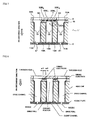
Classifications
-
- B—PERFORMING OPERATIONS; TRANSPORTING
- B41—PRINTING; LINING MACHINES; TYPEWRITERS; STAMPS
- B41J—TYPEWRITERS; SELECTIVE PRINTING MECHANISMS, i.e. MECHANISMS PRINTING OTHERWISE THAN FROM A FORME; CORRECTION OF TYPOGRAPHICAL ERRORS
- B41J2/00—Typewriters or selective printing mechanisms characterised by the printing or marking process for which they are designed
- B41J2/005—Typewriters or selective printing mechanisms characterised by the printing or marking process for which they are designed characterised by bringing liquid or particles selectively into contact with a printing material
- B41J2/01—Ink jet
- B41J2/135—Nozzles
- B41J2/14—Structure thereof only for on-demand ink jet heads
- B41J2/14201—Structure of print heads with piezoelectric elements
- B41J2/14209—Structure of print heads with piezoelectric elements of finger type, chamber walls consisting integrally of piezoelectric material
-
- B—PERFORMING OPERATIONS; TRANSPORTING
- B41—PRINTING; LINING MACHINES; TYPEWRITERS; STAMPS
- B41J—TYPEWRITERS; SELECTIVE PRINTING MECHANISMS, i.e. MECHANISMS PRINTING OTHERWISE THAN FROM A FORME; CORRECTION OF TYPOGRAPHICAL ERRORS
- B41J2/00—Typewriters or selective printing mechanisms characterised by the printing or marking process for which they are designed
- B41J2/005—Typewriters or selective printing mechanisms characterised by the printing or marking process for which they are designed characterised by bringing liquid or particles selectively into contact with a printing material
- B41J2/01—Ink jet
- B41J2/135—Nozzles
- B41J2/14—Structure thereof only for on-demand ink jet heads
- B41J2002/14491—Electrical connection
Definitions
- the present invention relates to an ink-jet head, and more particularly to an ink-jet head that has a head chip in which drive channels and dummy channels are alternately arranged and can achieve high density of channels.
- a shear mode type ink-jet head that subjects a drive wall to shearing deformation by applying a drive signal of a predetermined voltage to a drive electrode formed on the drive wall that partitions channels and discharges an ink in each channel from a nozzle by using a pressure produced at this moment
- a so-called harmonica-shaped head chip having opening portions of channels arranged in a front face and a rear face, respectively.
- each drive electrode faces the inside of a channel and is not exposed to the outside, how each drive electrode is electrically connected with a drive circuit is a problem.
- a channel row placed on the outer side can be easily electrically connected with, e.g., an FPC at an end portion of this head chip by forming a connection electrode that is electrically conductive relative to the drive electrode from each channel to the end portion of the head chip with use of a rear face of the head chip.
- connection electrode that is conducive with reach drive electrode must be formed to reach the end portion of the head chip across each channel row on the outer side.
- Patent Literature 1 discloses that four channel rows are arranged while shifting a channel pitch in increments of 1/4, drive electrodes in the respective channels are exposed around opening potions on a back side of a head chip to form respective electrical contacts, and a flexible substrate having a wiring electrode formed on one side thereof is attached to the back side of the head chip so as to cover the entire rear face while the wiring electrode forming surface is arranged to face the rear face of the head chip, whereby a drive signal can be applied from one lateral side of the head chip.
- a through-hole is formed at a position corresponding to each channel, and an ink can be supplied to each channel via this through-hole.
- a wiring electrode electrically connected with an electrical contact of each channel row placed on the inner side is formed between the through-holes adjacent to each other in the same channel row.
- up to three wiring electrodes run between the respective channels by shifting the pitch by 1/4 for each of the four channel rows. Since each wiring electrode runs between the through-holes adjacent to each other, each wiring electrode is arranged to be set in the range of a width (a thickness) of the drive wall as seen from a direction parallel to an ink discharge direction.
- the shear mode type ink-jet head there is an ink-jet head having an independently driven type head chip in which a channel row is configured by dividing respective channels in the channel row into drive channels that discharge an ink and dummy channels that do not discharge the ink and alternately arranging these channels. Alternately arranging the drive channels and the dummy channels enables discharging the ink from all the drive channels at the same time.
- Patent Literature 2 discloses that each connection electrode that is conductive relative to a drive electrode in each channel is formed on a rear face of such an independently driven type harmonica-shaped head chip, and a flexible substrate having each wiring electrode formed on one side thereof is used in a narrow shape having the same width as a width of the wiring electrode on a rear face of the head chip, and the connection electrode of each channel row placed on the inner side in a plurality of aligned channel rows is drawn to an end portion of the head chip across each channel row on the outer side.
- the flexible substrate having each wiring electrode formed thereon is provided to close an opening portion of each dummy channel on the rear face at the time of getting across the channel row on the outer side. Since the surface of the flexible substrate opposite to the wiring electrode forming surface faces the rear face of the head chip, it is possible to prevent occurrence of a short circuit of each drive electrode exposed in or near an opening portion of the dummy channel or the connection electrode. Further, since the flexible substrate is provided to close the opening portion of each dummy channel on the back side, it is possible to easily cope with high density of the channels.
- the wiring electrode can be prevented from directly coming into contact with the ink, but the wiring electrode that is wired across the channel rows runs on a drive wall between channels as seen from a direction parallel to an ink discharge direction, and hence a width of the drive wall becomes narrower as density of the channels increases, resulting in a problem that high density is hard to be realized.
- the wiring electrode must be narrowed as density of the channels increases and a space between channels (a width of the drive wall) through which the wiring electrode runs becomes narrower.
- electrical resistance increases, and there is a limit in narrowing.
- an object of the present invention to provide an ink-jet head that enables arranging wiring electrodes at high density and can easily cope with an increase in density of channels even if a substrate having the wiring electrodes is attached to a back side of an independently drive harmonica-shaped head chip having a plurality of channel rows in such a manner that the wiring electrodes are provided on the back side of the head chip.
- the ink-jet head that enables arranging wiring electrodes at high density and can easily cope with an increase in density of channels even if a substrate having the wiring electrodes is attached to a back side of an independently drive harmonica-shaped head chip having a plurality of channel rows in such a manner that the wiring electrodes are provided on the back side of the head chip.
- a head chip according to the present invention has a plurality of channels, each of which has channels and drive walls formed of piezoelectric elements alternately arranged, in parallel. Opening portions of the respective channels are arranged to face each other on a front face and a rear face of the head chip.
- Each channel is formed into a straight shape whose cross-sectional shape does not vary from the opening portion in the rear face (an inlet port of the channel) to the opening portion on the front face (an outlet portion of the channel), and a drive electrode is formed on a surface of the drive wall facing the inside of each channel.
- Such a head chip is a so-called shear mode type harmonica-shaped head chip formed of a hexahedron, and it causes shear deformation of the drive wall by applying a drive signal of a predetermined voltage to each drive electrode on both surfaces of the drive wall, and hence a pressure is changed for discharging an ink supplied into each channel, whereby ink drops are discharged from each nozzle arranged on the front side of the head chip.
- a surface on which each nozzle is arranged to discharge the ink is defined as a "front face”, and a surface on the opposite side is defined as a "rear face”. Further, a direction parallel to the front face or the rear face of the head chip which is also a direction to get away from the head chip is defined as a "lateral side”.
- the channel row in the present invention is an independently driven type head chip in which drive channels and dummy channels are alternately arranged.
- Connection electrodes that are conductive relative to the respective drive electrodes in the drive channels and the dummy channels are individually formed on the rear face of the head chip, and they are aligned on the rear face of the head chip at the same chip as the corresponding drive channels or dummy channels.
- the drive channel is a channel through which the ink is discharged from a nozzle in accordance with image data at the time of recording an image
- the dummy channel is a channel through which the ink is not always discharged. Since each dummy channel does not have to discharge the ink, and hence it is not generally charged with the ink, or a nozzle associated with each dummy channel is not formed on a nozzle plate.
- a wiring substrate attached to the rear face of the head chip through an adhesive is an intermediate wiring member that couples the head chip with a drive circuit. Preferably, it connects the head chip with an electrical wiring member from the drive circuit and facilities electrical connection with the electrical wiring member.
- This wiring substrate electrically draws each drive electrode to the lateral side orthogonal to the channel rows of the head chip through each corresponding connection electrode.
- the wiring substrate according to the present invention is attached to the back side of the head chip to cover all the channel rows opened in the rear face and have an end portion protruding toward the lateral side orthogonal to the channel rows in the head chip.
- This wiring substrate has through-holes, which enable supplying the ink into the drive channels, only at positions associated with the drive channels of the head chip. Therefore, the opening portions of the dummy channels on the back side are closed by this wiring substrate.
- the opening portion means a portion that is opened on a level with the rear face of the head chip.
- wiring electrodes that are electrically connected to the respective connection electrodes aligned on the rear face of the head chip are formed.
- one end of each wiring electrode is electrically connected with a corresponding connection electrode, and the other end of the same extends to the end portion of the wiring substrate protruding toward the lateral side of the head chip.
- At least one wiring electrode runs between the through-holes adjacent each other in at least one through-hole row of the plurality of through-holes in the wiring substrate associated with the channel rows in the head chip.
- This wiring electrode running between the through-holes is a wiring electrode that is electrically connected to the connection electrode in another channel row.
- At least one wiring electrode running between the through-holes is not in contact with the opening portion of the dummy channel and overlaps the opening portion of the dummy channel as seen from an ink discharge direction in a state that the wiring substrate is attached to the rear face of the head chip through an adhesive. That is, the wiring electrode running between the through-holes is not in contact with the rear face of the head chip except that it is in contact with the connection electrode to which the wiring electrode should be electrically conductive.
- an electrical wiring member having a wiring line that is electrically connected with the wiring electrode is attached to the end portion of the wiring substrate protruding toward the lateral side of the head chip.
- the electrical wiring member is connected with the drive circuit, and a voltage from the drive circuit is applied to the drive electrode through the wiring electrode and the connection electrode of the wiring substrate.
- the electrical wiring member a flexible printed circuit (which will be referred to as an FPC hereinafter) is preferably used.
- a substrate material of the wiring substrate in the present invention is any one of glass, silicon, and ceramics.
- rigidity is higher than that of a resin material having the same thickness, the wiring substrate can be thereby thinned, and channel resistance of each through-hole can be suppressed.
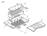
- FIG. 1 is an exploded perspective view of an ink-jet head
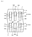
- FIG. 2 is a partial back view of the head chip.
- reference numeral 1 denotes a shear mode type harmonica-shaped head chip; 2, a nozzle plate; 3, a wiring substrate; and 4, a FPC
- This head chip 1 has two channel rows, i.e., a row A and a row B.
- a lower channel row in FIG. 2 is determined as the row A
- the upper channel row in the same is determined as the row B.
- drive channels 11A or 11B and dummy channels 12A or 12B are alternately arranged.
- Each drive wall 13A or 13B formed of a piezoelectric element is provided between each drive channel 11A or 11B and each dummy channel 12A or 12B adjacent thereto.
- Each drive channel 11A or 11B and each dummy channel 12A or 12B are opened in a front face 1a and a rear face 1b of the head chip 1, respectively, and drive electrodes 14 are hermetically formed on inner surfaces of the respective openings by, e.g., vapor deposition or sputtering.
- the drive channels 11A and the dummy channels 12A in the channel row which is the row A and the drive channels 11B and the dummy channels 12B in the channel row which is the row B are arranged to be shifted every pitch. That is, as seen along a direction that is parallel to the rear face 1b of the head chip 1 and orthogonal to the channel rows, the drive channels 11 A in the row A and the dummy channels 12B in the row B are placed on the same straight line, and the dummy channels 12A in the row A and the drive channels 11B in the row B are placed on the same straight line.
- connection electrodes 15A and 15B that achieve electrical conduction with the respective drive electrodes 14 of the drive channels 11A and 11B and the dummy channels 12A and 12B are formed by, e.g., vapor deposition or sputtering.
- One end of each connection electrode 15A or 15B achieves electrical conduction with the drive electrodes 14 in each corresponding drive channel 11A or 11B or each corresponding dummy channel 12A or 12B.
- the other end of each connection electrode 15A associated with the drive channel 11A and the dummy channel 12A in the row A is formed to reach one end edge 1c (a lower end edge in FIG.
- connection electrode 15B associated with the drive channel 11B and the dummy channel 12B in the row B is extended from the inside of each channel 11B or 12B toward the row A and formed to reach the front side of the channel row which is the row A. Therefore, both the connection electrodes 15A and 15B are extended from the respective channels 11A, 11B, 12A, and 12B in the same direction (a direction of an end edge 1c).
- a nozzle plate 2 is attached to the front face 1a of the head chip 1 through an adhesive.
- nozzles 21 are opened only at positions associated with the respective drive channels 11A and 11B.
- a wiring substrate 3 is a tabular substrate larger than an outer shape of the rear face 1b of the head chip 1. It is desirable for the wiring substrate 3 to be inflexible when it is attached to the rear face 1b of the head chip 1, and glass, silicon, or ceramics is preferably used. In this embodiment, a glass substrate was used.
- through-holes 32A and 32B through which an ink is supplied from a non-illustrated common ink chamber into the respective drive channels 11A and 11B are individually opened only at positions associated with the drive channels 11A and 11B opened in the rear face 1b of the head chip 1.
- An opening space of each through-hole 32A or 32B is formed to be equal to or slightly larger than an opening space of each drive channel 11A or 11B.
- the wiring substrate 3 prefferably has a thickness of 0.3 mm to 0.8 mm in terms of assuring appropriate rigidity while suppressing channel resistance of each through-hole 32A or 32B.
- each wiring electrode 33A or 33B which is electrically connected to each connection electrode 15A or 15B aligned on the rear face 1b of the head chip 1 on one-on-one level, is formed on the surface of the wiring substrate 3 by, e.g., plating, vapor deposition, or sputtering so as to extend in a direction crossing the channel rows in the head chip 1 on the surface of the wiring substrate 3.
- each wiring electrode 33A corresponding to the connection electrode 15A drawn from each channel 11A or 12A in the row A is placed in the vicinity associated with each channel 11A or 12A in the row A in a attaching region 31, and the other end of the same is extended from the attaching region 31 toward the lateral side orthogonal to the channel rows of the head chip 1 and protrudes from the attaching region 31 to reach the end portion 3a of the wiring substrate 3.
- each wiring electrode 33B corresponding to the connection electrode 15B drawn from each channel 11B or 12B in the row B is placed in the vicinity associated with each channel 11B or 12B in the row B in the attaching region 31, the other end of the same extends in the same direction as each wiring electrode 33A, runs between the through-holes 32A adjacent to each other in the row A, and protrudes from the attaching region 31 to reach the end portion 3 a of the wiring substrate 3, and each wiring electrode 33B and each wiring electrode 33A are alternately aligned.
- the wiring substrate 3 is positioned in such a manner that the respective wiring electrodes 33A and 33B are electrically connected with the respective corresponding connection electrodes 15A and 15B of the head chip 1, and it is attached to the rear face 1b of the head chip 1 through an adhesive.
- an adhesive an anisotropic conductive adhesive containing conductive particles may be used, but using an adhesive that does not contain conductive particles is preferable in terms of enhancement of certainty of short-circuit prevention.
- each wiring electrode 33B running between the through-holes 32A and 32A in the row A will now be further described hereinafter with reference to FIG. 3 to FIG. 5 .
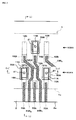
- FIG. 3 is a partial rear view showing a state that the wiring substrate 3 is attached to the rear face 1b of the head chip 1 from the back side of the wiring substrate 3
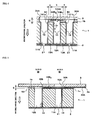
- FIG. 4 is a cross-sectional view taken along a line (iv)-(iv) in FIG. 3
- FIG. 5 is a cross-sectional view taken along a line (v)-(v) in FIG. 3 .
- the wiring electrodes that are conductive relative to the respective connection electrodes 15B in the row B are constituted of wiring electrodes 33B 1 electrically connected with the connection electrodes 15B in the drive channels 11 B in the row B and wiring electrodes 33B 2 electrically connected with the connection electrodes 15B in the dummy channels 12B in the row B.
- These wiring electrodes 33B 1 and 33B 2 runs between the through-holes 32A and 32A adjacent to each other in the row A and extend to the end portion 3a of the wiring substrate 3.
- a total of two wiring electrodes i.e., one wiring electrode 33B 1 electrically connected with the connection electrode 15B of one drive channel 11B and one wiring electrode 33B 2 electrically connected to the connection electrode 15B of one dummy channel 12B, which are adjacent to each other in the row B, are arranged between the through-holes 32A and 32A in the row A on the surface of the wiring substrate 3.
- the wiring electrode 33B 1 having one end electrically connected with the connection electrode 15B of the drive channel 11 B in the row B runs over the opening portion 120A of the dummy channel 12A in the row A so as to partially cover an edge portion 121b facing the edge portion 121a covered with the wiring electrode 33B 2 on the opening portion 120A of the dummy channel 12A in the row A placed between the through-holes 32A and 32A in the row A from a region connected with the connection electrode 15B on the other side, bends on the surface of the wiring substrate 3 toward the space between the connection electrodes 15A and 15A adjacent to each other in the row A toward the opposite side of the wiring electrode 33B 2 so as not to come into contact with the connection electrode 15A of the dummy channel 12A, and extends to the end portion 3a to be aligned with the wiring electrodes 33A and 33A electrically connected with the connection electrodes 15A and 15A.
- edge portions 121a and 121b of the opening portion 120A of the dummy channel 12A mean side edge portions of the drive electrode 14 on the opening side formed on the respective drive walls 13 facing each other in four side edges forming the peripheral edge of the opening portion 120A of the dummy channel 12A.
- the respective wiring electrodes 33B 1 and 33B 2 are arranged so as to partially overlap the edge portions 121a and 121b of the opening portion 120A of the dummy channel 12A as seen in an ink discharge direction (a direction extending from the upper side toward the lower side in FIG. 4 ).
- both the wiring electrodes 33B 1 and 33B 2 are hermetically formed on the surface of the wiring substrate 3, they are not in contact with the opening portion 120A of the dummy channel 12A, i.e., the rear face 1b of the head chip 1.
- the surface of each wiring electrode 33B 1 or 33B 2 is apart from the rear face 1b of the head chip 1 by a length corresponding to the thickness of each connection electrode 15A or 15B in a region except the region connected to the connection electrode 15B.
- each wiring electrode 33B 1 or 33B 2 is insulated from the rear face 1b of the head chip 1 by filling the space between these surfaces with an adhesive 50. Therefore, even if each wiring electrode 33B 1 or 33B 2 is arranged so as to overlap the opening portion 120A, it does not come into contact with the drive electrode 14 exposed in the opening portion 120A, and crosstalk or a short-circuit does not occur.
- a wiring space for each wiring electrode 33B 1 or 33B 2 is not restricted to the space corresponding to the thickness of the drive wall 13A, and a wide area extending between the through-holes 32A and 32A can be used, and hence each wiring electrode 33B 1 or 33B 2 can be widely formed. Therefore, an increase in electrical resistance of each wiring electrode 33B 1 or 33B 2 can be suppressed.
- each wiring line 33B 1 or 33B 2 running above the opening portion 120A of the dummy channel 12A in the row A is wired to overlap the opening portion 120A of the dummy channel 12A, bends so as to avoid the region of the connection electrode 15A in such a manner that it does not come into contact with the connection electrode 15A of the dummy channel 12A, and is aligned with the wiring electrode 33A at the end portion 3a of the wiring substrate 33.
- the number of channel rows may be three or more.
- FIG. 6 is a partial back view showing a state that a wiring substrate 3' is attached to a rear face 1b of the head chip 1' from a back side of the wiring substrate 3'
- FIG. 7 is a cross-sectional view taken along a line (vii)-(vii) in FIG. 6 .
- respective channel rows i.e., a row A and a row B have the same configuration as that of the head chip 1 including the above-explained two channel rows, and hence a description thereof will be omitted.
- parts denoted by the same reference signs as those in FIG. 3 and FIG. 4 are parts having the same configuration, and hence a detailed description thereof will be omitted.
- a channel row which is a channel C
- alignment is provided in such a manner that an alignment pitch of drive channels 11C and dummy channels 12C becomes the same as an alignment pitch of drive channels 11A and dummy channels 12A as channels in the row A.
- two wiring electrodes 33C run between through-holes 32B and 32B adjacent to each other in the row B of the wiring substrate 3', i.e., a wiring electrode 33C 1 electrically connected to a connection electrode 15C of the drive channel 11C in the row C and a wiring electrode 33C 2 electrically connected to a connection electrode 15C of a dummy channel 12C in the row C run so as to overlap opening portions 120B of the dummy channels 12B in the row B, and they have the same configuration as the wiring electrodes 33B 1 and 33B 2 running between the through-holes 32A and 32A in the row A in the embodiment of the two channel rows explained above.
- A is read as B and B is read as C in reference signs.
- wiring electrodes 33B 1 and 33B 2 electrically connected with the respective connection electrodes 15B in the row B and the wiring electrodes 33C 1 and 33C 2 electrically connected to the respective connection electrodes 15C in the row C are arranged between through-holes 32A and 31A in the row A.
- the wiring electrodes 33B 1 and 33C 1 placed on the inner side are arranged in the opening portion 120A so as to overlap the opening portion 120A of the dummy channel 12A in the row A, and each of the wiring electrodes 33B 2 and 33C 2 placed on the outer side is arranged in the range of a thickness of a drive wall 13A.
- the respective wiring electrodes 33B 1 , 33B 2 , 33C 1 , and 33C 2 are not in contact with the rear face 1b of the head chip 1, and an adhesive 50 fills a space between these electrodes and the rear face 1b.
- the total of four wiring electrodes 33B 1 , 33B 2 , 33C 1 , and 33C 2 can be arranged, thereby coping with an increase in density.
- the head chip 1 having the two channel rows shown in FIG. 1 to FIG. 5 can be formed as a head chip having four channel rows in which the two head chips 1 are aligned by configuring drawing directions of the wiring electrodes 33A and 33B on the surface of the wiring substrate 3 to be provided on both end sides to sandwich each head chip.
- a head chip having six channel rows can be likewise configured.
- a drive wall thickness of 59 ⁇ m, a channel width of 82 ⁇ m, and a through-hole width of 102 ⁇ m are provided as shown in Table 1.
- a machining accuracy or a attaching position accuracy of the head chip and the wiring substrate considering a machining accuracy or a attaching position accuracy of the head chip and the wiring substrate, in case of the comparative example, 20 ⁇ m or more must be assured as a length a1 between the wiring electrode and an adjacent through-hole and a length a2 between the wiring electrode and an opening portion of a dummy channel.
- a width of each wiring electrode is 9 ⁇ m at a maximum.
- Wiring that provides a width of 20 ⁇ m or less has high manufacturing difficulty level and, even if manufacture is possible, a wiring thickness must be reduced in proportion to the wiring width, and hence it can be expected that an increase in electrical resistance adversely affects ink discharge due to, e.g., a rise in drive voltage.
- channel density of up to approximately 120 dpi is a limit as shown in Table 1.
- Table 1 DENSITY NUMBER OF ROWS THICKNESS OF DRIVE WALL WIDTH OF CHANNEL WIDTH OF THROUGH-HOLE a1 a2 MAXIMUM WIDTH OF WIRING LINE PRACTICAL APPLICATION 180dpi 2 59 82 102 20 20 9 ⁇ 120dpi 2 89.5 122 142 20 20 39.5 ⁇
- a width of each wiring electrode can be set up to 46 ⁇ m, and 1/3 of the length b in FIG. 4 can be a width that allows each wiring electrode to run.
Landscapes
- Particle Formation And Scattering Control In Inkjet Printers (AREA)
- Coating Apparatus (AREA)
Abstract
Description
- The present invention relates to an ink-jet head, and more particularly to an ink-jet head that has a head chip in which drive channels and dummy channels are alternately arranged and can achieve high density of channels.
- As a shear mode type ink-jet head that subjects a drive wall to shearing deformation by applying a drive signal of a predetermined voltage to a drive electrode formed on the drive wall that partitions channels and discharges an ink in each channel from a nozzle by using a pressure produced at this moment, there is known a so-called harmonica-shaped head chip having opening portions of channels arranged in a front face and a rear face, respectively.
- In the harmonica-shaped head chip, since each drive electrode faces the inside of a channel and is not exposed to the outside, how each drive electrode is electrically connected with a drive circuit is a problem. In channel rows aligned in parallel in the head chip, a channel row placed on the outer side can be easily electrically connected with, e.g., an FPC at an end portion of this head chip by forming a connection electrode that is electrically conductive relative to the drive electrode from each channel to the end portion of the head chip with use of a rear face of the head chip. However, in case of applying a drive signal to each drive electrode of a channel row placed on the inner side from the end portion of the head chip, there is a problem that the connection electrode that is conducive with reach drive electrode must be formed to reach the end portion of the head chip across each channel row on the outer side.
- In conventional examples, to solve such a problem,
Patent Literature 1 discloses that four channel rows are arranged while shifting a channel pitch in increments of 1/4, drive electrodes in the respective channels are exposed around opening potions on a back side of a head chip to form respective electrical contacts, and a flexible substrate having a wiring electrode formed on one side thereof is attached to the back side of the head chip so as to cover the entire rear face while the wiring electrode forming surface is arranged to face the rear face of the head chip, whereby a drive signal can be applied from one lateral side of the head chip. - In this flexible substrate, a through-hole is formed at a position corresponding to each channel, and an ink can be supplied to each channel via this through-hole. A wiring electrode electrically connected with an electrical contact of each channel row placed on the inner side is formed between the through-holes adjacent to each other in the same channel row. In
Patent Literature 1, up to three wiring electrodes run between the respective channels by shifting the pitch by 1/4 for each of the four channel rows. Since each wiring electrode runs between the through-holes adjacent to each other, each wiring electrode is arranged to be set in the range of a width (a thickness) of the drive wall as seen from a direction parallel to an ink discharge direction. - Meanwhile, as the shear mode type ink-jet head, there is an ink-jet head having an independently driven type head chip in which a channel row is configured by dividing respective channels in the channel row into drive channels that discharge an ink and dummy channels that do not discharge the ink and alternately arranging these channels. Alternately arranging the drive channels and the dummy channels enables discharging the ink from all the drive channels at the same time.
-
Patent Literature 2 discloses that each connection electrode that is conductive relative to a drive electrode in each channel is formed on a rear face of such an independently driven type harmonica-shaped head chip, and a flexible substrate having each wiring electrode formed on one side thereof is used in a narrow shape having the same width as a width of the wiring electrode on a rear face of the head chip, and the connection electrode of each channel row placed on the inner side in a plurality of aligned channel rows is drawn to an end portion of the head chip across each channel row on the outer side. - The flexible substrate having each wiring electrode formed thereon is provided to close an opening portion of each dummy channel on the rear face at the time of getting across the channel row on the outer side. Since the surface of the flexible substrate opposite to the wiring electrode forming surface faces the rear face of the head chip, it is possible to prevent occurrence of a short circuit of each drive electrode exposed in or near an opening portion of the dummy channel or the connection electrode. Further, since the flexible substrate is provided to close the opening portion of each dummy channel on the back side, it is possible to easily cope with high density of the channels.
-
- Patent Document 1:
JP-A-2002-178509 - Patent Document 2:
JP-A-2008-143167 - Usually, in the harmonica-shaped head chip, an ink is supplied from the back side to each channel. Therefore, when each wiring electrode is exposed on the back side of the head chip like the description in
Patent Literature 2, the wiring electrode directly comes into contact with the ink, and there occurs a problem of corrosion of each electrode. - To avoid direct contact of the electrode and the ink, forming a top coat on an electrode surface is generally known, but the ink to be adopted may possibly penetrate, and there is still a problem to be solved in terms of avoidance of corrosion of each electrode.
- In case of arranging the wiring electrode to face the rear face of the head chip like the description in
Patent Document 1, the wiring electrode can be prevented from directly coming into contact with the ink, but the wiring electrode that is wired across the channel rows runs on a drive wall between channels as seen from a direction parallel to an ink discharge direction, and hence a width of the drive wall becomes narrower as density of the channels increases, resulting in a problem that high density is hard to be realized. - That is, according to the technology disclosed in
Patent Document 1, the wiring electrode must be narrowed as density of the channels increases and a space between channels (a width of the drive wall) through which the wiring electrode runs becomes narrower. However, when the wiring electrode is narrowed, electrical resistance increases, and there is a limit in narrowing. - Therefore, it is an object of the present invention to provide an ink-jet head that enables arranging wiring electrodes at high density and can easily cope with an increase in density of channels even if a substrate having the wiring electrodes is attached to a back side of an independently drive harmonica-shaped head chip having a plurality of channel rows in such a manner that the wiring electrodes are provided on the back side of the head chip.
- Any other object of the present invention will become apparent in the following description.
- The above object is achieved by each of the following inventions.
-
- 1. An ink-jet head comprising:
- a head chip in which a plurality of channel rows each having channels and drive walls formed of piezoelectric elements alternately arranged therein and also having drive electrodes formed on the drive walls each facing the inside of the channel are arranged, opening portions of the channels are arranged in each of a front face and a rear face, connection electrodes electrically conductive with respect to the drive electrodes in the channels are formed on the rear face, and each channel row is configured by alternately arranging drive channels from which an ink is discharged and dummy channels from which the ink is not discharged; and
- a wiring substrate that is attached to the rear face of the head chip so as to cover the plurality of channel rows and protrude toward a lateral side of the head chip,
- each of the connection electrodes being electrically drawn to an end portion of the wiring substrate by electrically connecting wiring electrodes formed on a surface of the wiring substrate attached to the head chip with the connection electrodes, the ink in the drive channels being discharged from nozzles by applying a voltage to the drive electrodes through the wiring electrodes and the connection electrodes,
- wherein, in the wiring substrate, each through-hole for ink supply is formed only at a position corresponding to the opening portion of each drive channel, at least one wiring electrode runs between the through-holes adjacent to each other in at least one through-hole row of a plurality of through-hole rows associated with the channel rows and extends to the end portion of the wiring substrate protruding toward the lateral side of the head chip, and
- at least one wiring electrode running between the through-holes is not in contact with the opening portion of the dummy channel and overlaps the opening portion of the dummy channel as seen from an ink discharge direction.
- 2. The ink-jet head according to 1,
wherein the wiring substrate is made of any one of glass, silicon, and ceramics. - 3. The ink-jet head according to 1 or 2,
wherein the head chip has two channel rows which are a row A and a row B, and
a total of two wiring electrodes, which are one wiring electrode associated with the drive channel in the row B and one wiring electrode associated with the dummy channel in the row B adjacent to the drive channel in the wiring electrodes electrically connected to the connection electrodes in the channel row B, run between the through-holes in the one row A. - 4. The ink-jet head according to 1 or 2,
wherein the head chip has three channel rows which are a row A, row B, and a row C,
a total of two wiring electrodes, which are one wiring electrode associated with the drive channel in the row C and one wiring electrode associated with the dummy channel in the row C adjacent to the drive channel in the wiring electrodes electrically connected to the connection electrodes in the channel row C, run between the through-holes in one row B, and
a total of four wiring electrodes, which are two wiring electrodes, i.e., one wiring electrode associated with the drive channel in the row B and one wiring electrode associated with the dummy channel in the row B adjacent to the drive channel in the row B in the wiring electrodes electrically connected to the connection electrodes in the channel row B and two wiring electrodes, i.e., one wiring electrode associated with the drive channel in the row C and one wiring electrode associated with the dummy channel in the row C adjacent to the drive channel in the row C, run between the through-holes in one row A. - According to the present invention, it is possible to provide the ink-jet head that enables arranging wiring electrodes at high density and can easily cope with an increase in density of channels even if a substrate having the wiring electrodes is attached to a back side of an independently drive harmonica-shaped head chip having a plurality of channel rows in such a manner that the wiring electrodes are provided on the back side of the head chip.
-
-
FIG. 1 is an exploded perspective view of an ink-jet head according to the present invention; -
FIG. 2 is a partial back view of a head chip according to the present invention; -
FIG. 3 is a partial back view showing a attaching state of the head chip and a wiring substrate; -
FIG. 4 is a cross-sectional view taken along a line (iv)-(iv) inFIG. 3 ; -
FIG. 5 is a cross-sectional view taken along a line (v)-(v) inFIG. 3 ; -
FIG. 6 is a partial back view showing a attaching state of the head chip including three channel rows and the wiring substrate; -
FIG. 7 is a cross-sectional view taken along a line (vii)-(vii) inFIG. 6 ; and -
FIG. 8 is a partial cross-sectional view of an ink-jet head showing a comparative example. - A head chip according to the present invention has a plurality of channels, each of which has channels and drive walls formed of piezoelectric elements alternately arranged, in parallel. Opening portions of the respective channels are arranged to face each other on a front face and a rear face of the head chip. Each channel is formed into a straight shape whose cross-sectional shape does not vary from the opening portion in the rear face (an inlet port of the channel) to the opening portion on the front face (an outlet portion of the channel), and a drive electrode is formed on a surface of the drive wall facing the inside of each channel.
- Such a head chip is a so-called shear mode type harmonica-shaped head chip formed of a hexahedron, and it causes shear deformation of the drive wall by applying a drive signal of a predetermined voltage to each drive electrode on both surfaces of the drive wall, and hence a pressure is changed for discharging an ink supplied into each channel, whereby ink drops are discharged from each nozzle arranged on the front side of the head chip.
- According to the present invention, in such a hexahedral harmonica-shaped head chip, a surface on which each nozzle is arranged to discharge the ink is defined as a "front face", and a surface on the opposite side is defined as a "rear face". Further, a direction parallel to the front face or the rear face of the head chip which is also a direction to get away from the head chip is defined as a "lateral side".
- The channel row in the present invention is an independently driven type head chip in which drive channels and dummy channels are alternately arranged. Connection electrodes that are conductive relative to the respective drive electrodes in the drive channels and the dummy channels are individually formed on the rear face of the head chip, and they are aligned on the rear face of the head chip at the same chip as the corresponding drive channels or dummy channels.
- The drive channel is a channel through which the ink is discharged from a nozzle in accordance with image data at the time of recording an image, and the dummy channel is a channel through which the ink is not always discharged. Since each dummy channel does not have to discharge the ink, and hence it is not generally charged with the ink, or a nozzle associated with each dummy channel is not formed on a nozzle plate.
- A wiring substrate attached to the rear face of the head chip through an adhesive is an intermediate wiring member that couples the head chip with a drive circuit. Preferably, it connects the head chip with an electrical wiring member from the drive circuit and facilities electrical connection with the electrical wiring member. This wiring substrate electrically draws each drive electrode to the lateral side orthogonal to the channel rows of the head chip through each corresponding connection electrode.
- The wiring substrate according to the present invention is attached to the back side of the head chip to cover all the channel rows opened in the rear face and have an end portion protruding toward the lateral side orthogonal to the channel rows in the head chip.
- This wiring substrate has through-holes, which enable supplying the ink into the drive channels, only at positions associated with the drive channels of the head chip. Therefore, the opening portions of the dummy channels on the back side are closed by this wiring substrate.
- It is to be noted that the opening portion means a portion that is opened on a level with the rear face of the head chip.
- On a surface of the wiring substrate that is attached to the head chip (which will be referred to as a front side hereinafter), wiring electrodes that are electrically connected to the respective connection electrodes aligned on the rear face of the head chip are formed. In a state that this wiring substrate is attached to the rear face of the head chip, one end of each wiring electrode is electrically connected with a corresponding connection electrode, and the other end of the same extends to the end portion of the wiring substrate protruding toward the lateral side of the head chip.
- At least one wiring electrode runs between the through-holes adjacent each other in at least one through-hole row of the plurality of through-holes in the wiring substrate associated with the channel rows in the head chip. This wiring electrode running between the through-holes is a wiring electrode that is electrically connected to the connection electrode in another channel row.
- At least one wiring electrode running between the through-holes is not in contact with the opening portion of the dummy channel and overlaps the opening portion of the dummy channel as seen from an ink discharge direction in a state that the wiring substrate is attached to the rear face of the head chip through an adhesive. That is, the wiring electrode running between the through-holes is not in contact with the rear face of the head chip except that it is in contact with the connection electrode to which the wiring electrode should be electrically conductive.
- As a result, even if the wiring substrate is attached to the entire rear face of the head chip in such a manner that the wiring electrode is provided on the back side of the head chip, since the wiring electrode does not come into contact with the rear face of the head chip except the connection electrode of the corresponding channel, crosstalk and a short-circuit can be prevented from occurring. Furthermore, since at least one wiring electrode running between the through-holes runs above the opening portion of the dummy channel, an entire space between the adjoining through-holes including the upper side of the opening portion of the dummy channel can be used even though a space between the channels is small, and hence high-density wiring is possible without considerably reducing a width of each wiring electrode, thus coping with high density of the channels.
- In such an ink-jet head, an electrical wiring member having a wiring line that is electrically connected with the wiring electrode is attached to the end portion of the wiring substrate protruding toward the lateral side of the head chip. The electrical wiring member is connected with the drive circuit, and a voltage from the drive circuit is applied to the drive electrode through the wiring electrode and the connection electrode of the wiring substrate. As a result, the ink in the drive channel can be discharged from the nozzle. As the electrical wiring member, a flexible printed circuit (which will be referred to as an FPC hereinafter) is preferably used.
- It is preferable for a substrate material of the wiring substrate in the present invention to be any one of glass, silicon, and ceramics. When such a material is used, rigidity is higher than that of a resin material having the same thickness, the wiring substrate can be thereby thinned, and channel resistance of each through-hole can be suppressed.
- An embodiment according to the present invention will now be described hereinafter with reference to the drawings.
-
FIG. 1 is an exploded perspective view of an ink-jet head, andFIG. 2 is a partial back view of the head chip. - In the drawings,
reference numeral 1 denotes a shear mode type harmonica-shaped head chip; 2, a nozzle plate; 3, a wiring substrate; and 4, a FPC - This
head chip 1 has two channel rows, i.e., a row A and a row B. Here, a lower channel row inFIG. 2 is determined as the row A, and the upper channel row in the same is determined as the row B. In each channel row,drive channels dummy channels drive wall drive channel dummy channel drive channel dummy channel rear face 1b of thehead chip 1, respectively, and driveelectrodes 14 are hermetically formed on inner surfaces of the respective openings by, e.g., vapor deposition or sputtering. - It is to be noted that, in the
head chip 1, thedrive channels 11A and thedummy channels 12A in the channel row which is the row A and thedrive channels 11B and thedummy channels 12B in the channel row which is the row B are arranged to be shifted every pitch. That is, as seen along a direction that is parallel to therear face 1b of thehead chip 1 and orthogonal to the channel rows, thedrive channels 11 A in the row A and thedummy channels 12B in the row B are placed on the same straight line, and thedummy channels 12A in the row A and thedrive channels 11B in the row B are placed on the same straight line. - On the
rear face 1b of thehead chip 1,connection electrodes respective drive electrodes 14 of thedrive channels dummy channels connection electrode drive electrodes 14 in eachcorresponding drive channel corresponding dummy channel connection electrode 15A associated with thedrive channel 11A and thedummy channel 12A in the row A is formed to reach oneend edge 1c (a lower end edge inFIG. 2 ) of thehead chip 1 from the inside of eachchannel connection electrode 15B associated with thedrive channel 11B and thedummy channel 12B in the row B is extended from the inside of eachchannel connection electrodes respective channels end edge 1c). - A
nozzle plate 2 is attached to the front face 1a of thehead chip 1 through an adhesive. In thenozzle plate 2,nozzles 21 are opened only at positions associated with therespective drive channels - A
wiring substrate 3 is a tabular substrate larger than an outer shape of therear face 1b of thehead chip 1. It is desirable for thewiring substrate 3 to be inflexible when it is attached to therear face 1b of thehead chip 1, and glass, silicon, or ceramics is preferably used. In this embodiment, a glass substrate was used. - In a attaching region that is attached to the
rear face 1b of the head chip 1 (a region indicated by an alternate long and short dash line inFIG. 1 ), through-holes respective drive channels drive channels rear face 1b of thehead chip 1. An opening space of each through-hole drive channel - It is preferable for the
wiring substrate 3 to have a thickness of 0.3 mm to 0.8 mm in terms of assuring appropriate rigidity while suppressing channel resistance of each through-hole - Moreover, each
wiring electrode connection electrode rear face 1b of thehead chip 1 on one-on-one level, is formed on the surface of thewiring substrate 3 by, e.g., plating, vapor deposition, or sputtering so as to extend in a direction crossing the channel rows in thehead chip 1 on the surface of thewiring substrate 3. - One end of each
wiring electrode 33A corresponding to theconnection electrode 15A drawn from eachchannel channel region 31, and the other end of the same is extended from the attachingregion 31 toward the lateral side orthogonal to the channel rows of thehead chip 1 and protrudes from the attachingregion 31 to reach theend portion 3a of thewiring substrate 3. - On the other hand, one end of each
wiring electrode 33B corresponding to theconnection electrode 15B drawn from eachchannel channel region 31, the other end of the same extends in the same direction as eachwiring electrode 33A, runs between the through-holes 32A adjacent to each other in the row A, and protrudes from the attachingregion 31 to reach theend portion 3 a of thewiring substrate 3, and eachwiring electrode 33B and eachwiring electrode 33A are alternately aligned. - The
wiring substrate 3 is positioned in such a manner that therespective wiring electrodes corresponding connection electrodes head chip 1, and it is attached to therear face 1b of thehead chip 1 through an adhesive. As the adhesive, an anisotropic conductive adhesive containing conductive particles may be used, but using an adhesive that does not contain conductive particles is preferable in terms of enhancement of certainty of short-circuit prevention. - Particulars of each
wiring electrode 33B running between the through-holes FIG. 3 to FIG. 5 . -
FIG. 3 is a partial rear view showing a state that thewiring substrate 3 is attached to therear face 1b of thehead chip 1 from the back side of thewiring substrate 3,FIG. 4 is a cross-sectional view taken along a line (iv)-(iv) inFIG. 3 , andFIG. 5 is a cross-sectional view taken along a line (v)-(v) inFIG. 3 . - The wiring electrodes that are conductive relative to the
respective connection electrodes 15B in the row B are constituted ofwiring electrodes 33B1 electrically connected with theconnection electrodes 15B in thedrive channels 11 B in the row B andwiring electrodes 33B2 electrically connected with theconnection electrodes 15B in thedummy channels 12B in the row B. Thesewiring electrodes holes end portion 3a of thewiring substrate 3. A total of two wiring electrodes, i.e., onewiring electrode 33B1 electrically connected with theconnection electrode 15B of onedrive channel 11B and onewiring electrode 33B2 electrically connected to theconnection electrode 15B of onedummy channel 12B, which are adjacent to each other in the row B, are arranged between the through-holes wiring substrate 3. - The
wiring electrode 33B2 having one end electrically connected with theconnection electrode 15B of thedummy channel 12B in the row B bends on the surface of thewiring substrate 3 from a region connected to theconnection electrode 15B toward the space between the through-holes opening portion 120A of thedummy channel 12A in the row A placed between the through-holes edge portion 121 a of theopening portion 120A, further bends on the surface of thewiring substrate 3 toward the space between theconnection electrodes connection electrode 15A of thedummy channel 12A, and extends to theend portion 3 a to be aligned with thewiring electrodes connection electrodes - Further, the
wiring electrode 33B1 having one end electrically connected with theconnection electrode 15B of thedrive channel 11 B in the row B runs over the openingportion 120A of thedummy channel 12A in the row A so as to partially cover anedge portion 121b facing theedge portion 121a covered with thewiring electrode 33B2 on theopening portion 120A of thedummy channel 12A in the row A placed between the through-holes connection electrode 15B on the other side, bends on the surface of thewiring substrate 3 toward the space between theconnection electrodes wiring electrode 33B2 so as not to come into contact with theconnection electrode 15A of thedummy channel 12A, and extends to theend portion 3a to be aligned with thewiring electrodes connection electrodes - It is to be noted that the
edge portions opening portion 120A of thedummy channel 12A mean side edge portions of thedrive electrode 14 on the opening side formed on the respective drive walls 13 facing each other in four side edges forming the peripheral edge of theopening portion 120A of thedummy channel 12A. - As described above, in the ink-jet head according to the present invention, when each of the
wiring electrodes holes head chip 1, it partially protrudes toward not only the inside of the space above eachdrive wall 13A in the row A on therear face 1b of thehead chip 1 but also the inside of theopening portion 120A of thedummy channel 12A from this space by a length corresponding to a protruding amount c as shown inFIG. 4 . Further, therespective wiring electrodes edge portions opening portion 120A of thedummy channel 12A as seen in an ink discharge direction (a direction extending from the upper side toward the lower side inFIG. 4 ). - Since both the
wiring electrodes wiring substrate 3, they are not in contact with theopening portion 120A of thedummy channel 12A, i.e., therear face 1b of thehead chip 1. As shown inFIG. 4 and FIG. 5 , since a gap S corresponding to a thickness of eachconnection electrode wiring electrode head chip 1 and thewiring substrate 3, the surface of eachwiring electrode rear face 1b of thehead chip 1 by a length corresponding to the thickness of eachconnection electrode connection electrode 15B. The surface of eachwiring electrode rear face 1b of thehead chip 1 by filling the space between these surfaces with an adhesive 50. Therefore, even if eachwiring electrode opening portion 120A, it does not come into contact with thedrive electrode 14 exposed in theopening portion 120A, and crosstalk or a short-circuit does not occur. - Furthermore, a wiring space for each
wiring electrode drive wall 13A, and a wide area extending between the through-holes wiring electrode wiring electrode - It is to be noted that each
wiring line opening portion 120A of thedummy channel 12A in the row A is wired to overlap theopening portion 120A of thedummy channel 12A, bends so as to avoid the region of theconnection electrode 15A in such a manner that it does not come into contact with theconnection electrode 15A of thedummy channel 12A, and is aligned with thewiring electrode 33A at theend portion 3a of the wiring substrate 33. - Although the structure including the two channel rows, i.e., the row A and the row B provided in the
head chip 1 has been exemplified in the foregoing embodiment, the number of channel rows may be three or more. - A description will now be given as to an ink-jet head using a head chip 1' including three channel rows, i.e., a row A, a row B, and a row C with reference to
FIG. 6 andFIG. 7 . -
FIG. 6 is a partial back view showing a state that a wiring substrate 3' is attached to arear face 1b of the head chip 1' from a back side of the wiring substrate 3', andFIG. 7 is a cross-sectional view taken along a line (vii)-(vii) inFIG. 6 . It is to be noted that, in this head chip 1', respective channel rows, i.e., a row A and a row B have the same configuration as that of thehead chip 1 including the above-explained two channel rows, and hence a description thereof will be omitted. Furthermore, parts denoted by the same reference signs as those inFIG. 3 andFIG. 4 are parts having the same configuration, and hence a detailed description thereof will be omitted. - In a channel row which is a channel C, alignment is provided in such a manner that an alignment pitch of
drive channels 11C anddummy channels 12C becomes the same as an alignment pitch ofdrive channels 11A anddummy channels 12A as channels in the row A. - In this embodiment, two wiring electrodes 33C run between through-
holes connection electrode 15C of thedrive channel 11C in the row C and a wiring electrode 33C2 electrically connected to aconnection electrode 15C of adummy channel 12C in the row C run so as to overlap openingportions 120B of thedummy channels 12B in the row B, and they have the same configuration as thewiring electrodes holes - On the other hand, a total of four wiring electrodes, i.e.,
wiring electrodes respective connection electrodes 15B in the row B and the wiring electrodes 33C1 and 33C2 electrically connected to therespective connection electrodes 15C in the row C are arranged between through-holes 32A and 31A in the row A. - At this time, as shown in
FIG. 7 , as seen in an ink discharge direction, thewiring electrodes 33B1 and 33C1 placed on the inner side are arranged in theopening portion 120A so as to overlap theopening portion 120A of thedummy channel 12A in the row A, and each of thewiring electrodes 33B2 and 33C2 placed on the outer side is arranged in the range of a thickness of adrive wall 13A. Therespective wiring electrodes rear face 1b of thehead chip 1, and an adhesive 50 fills a space between these electrodes and therear face 1b. - As described above, according to the present invention, when the entire space between the through-
holes wiring electrodes - It is to be noted that the
head chip 1 having the two channel rows shown inFIG. 1 to FIG. 5 can be formed as a head chip having four channel rows in which the twohead chips 1 are aligned by configuring drawing directions of thewiring electrodes wiring substrate 3 to be provided on both end sides to sandwich each head chip. Moreover, in case of the head chip 1' having the three channel rows shown inFIG. 6 andFIG. 7 , a head chip having six channel rows can be likewise configured. - In a head chip including two channel rows, channel density that enables wiring was verified in regard to a case where wiring electrodes on a surface of a wiring substrate are formed as shown in
FIG. 3 to FIG. 5 (the present invention) and a case where two wiring electrodes between through-holes adjacent to each other are formed on drive walls so that they do not overlap an opening portion of each dummy channel as shown inFIG. 8 (a comparative example). - When the channel density is 180 dpi (dot per inch), a drive wall thickness of 59 µm, a channel width of 82 µm, and a through-hole width of 102 µm are provided as shown in Table 1.
- Here, considering a machining accuracy or a attaching position accuracy of the head chip and the wiring substrate, in case of the comparative example, 20 µm or more must be assured as a length a1 between the wiring electrode and an adjacent through-hole and a length a2 between the wiring electrode and an opening portion of a dummy channel. In this case, a width of each wiring electrode is 9 µm at a maximum. Wiring that provides a width of 20 µm or less has high manufacturing difficulty level and, even if manufacture is possible, a wiring thickness must be reduced in proportion to the wiring width, and hence it can be expected that an increase in electrical resistance adversely affects ink discharge due to, e.g., a rise in drive voltage.
- Therefore, in case of this comparative example, to realize a practicable wiring width, channel density of up to approximately 120 dpi is a limit as shown in Table 1.
[Table 1] DENSITY NUMBER OF ROWS THICKNESS OF DRIVE WALL WIDTH OF CHANNEL WIDTH OF THROUGH-HOLE a1 a2 MAXIMUM WIDTH OF WIRING LINE PRACTICAL APPLICATION 180dpi 2 59 82 102 20 20 9 × 120dpi 2 89.5 122 142 20 20 39.5 ○ - On the other hand, in case of the present invention, as shown in Table 2, even if channel density of 180 dpi is provided, a width of each wiring electrode can be set up to 46 µm, and 1/3 of the length b in
FIG. 4 can be a width that allows each wiring electrode to run. - In case of the two channel rows, it can be understood that, even if 300 dpi is provided, a wiring width of 22 µm can be assured and higher density than that in the comparative example can be achieved.
- Additionally, in case of the present invention, even if three channel rows are provided, 1/7 of the length b enables each wiring electrode to run, and channel density of 180 dpi can be realized.
[Table 2] DENSITY NUMBER OF ROWS THICKNESS OF DRIVE WALL WIDTH OF CHANNEL WIDTH OF THROUGH-HOLE a b* MAXIMUM WIDTH OF WIRING LINE PRACTICAL APPLICATION 180dpi 2 59 82 102 20 140 46 ○ 180dpi 3 59 82 102 20 140 20 ○ 300dpi 2 42 43 63 20 67 22 ○ *Since the width of each through-hole is larger than the width of each channel, b=drive wall × 2+width of each channel-20-a×2. -
- 1, 1': head chip
- 1a: front face
- 1b: rear face
- 1c: end edge
- 11 A, 11B, 11C: drive channel
- 12A, 12B, 12C: dummy channel
- 120A, 120B: opening portion
- 121a, 121b: edge portion
- 13A, 13B: drive wall
- 14: drive electrode
- 15A, 15B: connection electrode
- 2: nozzle plate
- 21: nozzle
- 3, 3': wiring substrate
- 3a: end portion
- 31: attaching region
- 32A, 32B, 32C: through-hole
- 33A, 33B, 33B1, 33B2, 33C1, 33C2: wiring electrode
- 4: FPC
- 50: adhesive
Claims (4)
- An ink-jet head comprising:a head chip in which a plurality of channel rows each having channels and drive walls formed of piezoelectric elements alternately arranged therein and also having drive electrodes formed on the drive walls each facing the inside of the channel are arranged, opening portions of the channels are arranged in each of a front face and a rear face, connection electrodes electrically conductive with respect to the drive electrodes in the channels are formed on the rear face, and each channel row is configured by alternately arranging drive channels from which an ink is discharged and dummy channels from which the ink is not discharged; anda wiring substrate that is attached to the rear face of the head chip so as to cover the plurality of channel rows and protrude toward a lateral side of the head chip,each of the connection electrodes being electrically drawn to an end portion of the wiring substrate by electrically connecting wiring electrodes formed on a surface of the wiring substrate attached to the head chip with the connection electrodes, the ink in the drive channels being discharged from nozzles by applying a voltage to the drive electrodes through the wiring electrodes and the connection electrodes,wherein, in the wiring substrate, each through-hole for ink supply is formed only at a position corresponding to the opening portion of each drive channel, at least one wiring electrode runs between the through-holes adjacent to each other in at least one through-hole row of a plurality of through-hole rows associated with the channel rows and extends to the end portion of the wiring substrate protruding toward the lateral side of the head chip, andat least one wiring electrode running between the through-holes is not in contact with the opening portion of the dummy channel and overlaps the opening portion of the dummy channel as seen from an ink discharge direction.
- The ink-jet head according to claim 1,
wherein the wiring substrate is made of any one of glass, silicon, and ceramics. - The ink-jet head according to claim 1 or 2,
wherein the head chip has two channel rows which are a row A and a row B, and
a total of two wiring electrodes, which are one wiring electrode associated with the drive channel in the row B and one wiring electrode associated with the dummy channel in the row B adjacent to the drive channel in the wiring electrodes electrically connected to the connection electrodes in the channel row B, run between the through-holes in the one row A. - The ink-jet head according to claim 1 or 2,
wherein the head chip has three channel rows which are a row A, row B, and a row C,
a total of two wiring electrodes, which are one wiring electrode associated with the drive channel in the row C and one wiring electrode associated with the dummy channel in the row C adjacent to the drive channel in the wiring electrodes electrically connected to the connection electrodes in the channel row C, run between the through-holes in one row B, and
a total of four wiring electrodes, which are two wiring electrodes, i.e., one wiring electrode associated with the drive channel in the row B and one wiring electrode associated with the dummy channel in the row B adjacent to the drive channel in the row B in the wiring electrodes electrically connected to the connection electrodes in the channel row B and two wiring electrodes, i.e., one wiring electrode associated with the drive channel in the row C and one wiring electrode associated with the dummy channel in the row C adjacent to the drive channel in the row C, run between the through-holes in one row A.
Applications Claiming Priority (2)
| Application Number | Priority Date | Filing Date | Title |
|---|---|---|---|
| JP2011096615 | 2011-04-22 | ||
| PCT/JP2012/060716 WO2012144597A1 (en) | 2011-04-22 | 2012-04-20 | Ink-jet head |
Publications (3)
| Publication Number | Publication Date |
|---|---|
| EP2700506A1 true EP2700506A1 (en) | 2014-02-26 |
| EP2700506A4 EP2700506A4 (en) | 2015-07-22 |
| EP2700506B1 EP2700506B1 (en) | 2017-07-19 |
Family
ID=47041701
Family Applications (1)
| Application Number | Title | Priority Date | Filing Date |
|---|---|---|---|
| EP12774310.2A Active EP2700506B1 (en) | 2011-04-22 | 2012-04-20 | Ink-jet head |
Country Status (3)
| Country | Link |
|---|---|
| EP (1) | EP2700506B1 (en) |
| JP (1) | JP5846201B2 (en) |
| WO (1) | WO2012144597A1 (en) |
Cited By (1)
| Publication number | Priority date | Publication date | Assignee | Title |
|---|---|---|---|---|
| US9352565B2 (en) | 2012-11-05 | 2016-05-31 | Sii Printek Inc. | Liquid jet head and liquid jet apparatus |
Families Citing this family (5)
| Publication number | Priority date | Publication date | Assignee | Title |
|---|---|---|---|---|
| JP6278588B2 (en) * | 2012-09-24 | 2018-02-14 | エスアイアイ・プリンテック株式会社 | Liquid ejecting head and liquid ejecting apparatus |
| JP5939966B2 (en) | 2012-11-22 | 2016-06-29 | エスアイアイ・プリンテック株式会社 | Liquid ejecting head, liquid ejecting apparatus, and method of manufacturing liquid ejecting head |
| JP5888227B2 (en) * | 2012-12-28 | 2016-03-16 | コニカミノルタ株式会社 | Ink jet head and method of manufacturing ink jet head |
| JP5995718B2 (en) * | 2012-12-28 | 2016-09-21 | エスアイアイ・プリンテック株式会社 | Head chip, head chip manufacturing method, liquid ejecting head, and liquid ejecting apparatus |
| JP6209383B2 (en) | 2013-07-24 | 2017-10-04 | エスアイアイ・プリンテック株式会社 | Liquid ejecting head, liquid ejecting apparatus, and method of manufacturing liquid ejecting head |
Family Cites Families (8)
| Publication number | Priority date | Publication date | Assignee | Title |
|---|---|---|---|---|
| JP2001010110A (en) * | 1999-06-29 | 2001-01-16 | Kyocera Corp | Recording head |
| JP2002178509A (en) | 2000-12-12 | 2002-06-26 | Olympus Optical Co Ltd | Liquid drop jet apparatus |
| JP3795359B2 (en) * | 2001-09-11 | 2006-07-12 | シャープ株式会社 | Inkjet head |
| JP2003326710A (en) * | 2002-05-14 | 2003-11-19 | Sharp Corp | Method for forming protective film and ink jet head using the same |
| JP4622359B2 (en) * | 2004-07-22 | 2011-02-02 | コニカミノルタホールディングス株式会社 | Inkjet head manufacturing method |
| JP5056309B2 (en) * | 2006-11-16 | 2012-10-24 | コニカミノルタIj株式会社 | Inkjet head |
| JP2009226677A (en) * | 2008-03-21 | 2009-10-08 | Konica Minolta Ij Technologies Inc | Inkjet head |
| JP5304021B2 (en) * | 2008-05-14 | 2013-10-02 | コニカミノルタ株式会社 | Inkjet head manufacturing method |
-
2012
- 2012-04-20 JP JP2013511055A patent/JP5846201B2/en active Active
- 2012-04-20 EP EP12774310.2A patent/EP2700506B1/en active Active
- 2012-04-20 WO PCT/JP2012/060716 patent/WO2012144597A1/en not_active Ceased
Cited By (1)
| Publication number | Priority date | Publication date | Assignee | Title |
|---|---|---|---|---|
| US9352565B2 (en) | 2012-11-05 | 2016-05-31 | Sii Printek Inc. | Liquid jet head and liquid jet apparatus |
Also Published As
| Publication number | Publication date |
|---|---|
| EP2700506B1 (en) | 2017-07-19 |
| EP2700506A4 (en) | 2015-07-22 |
| JP5846201B2 (en) | 2016-01-20 |
| JPWO2012144597A1 (en) | 2014-07-28 |
| WO2012144597A1 (en) | 2012-10-26 |
Similar Documents
| Publication | Publication Date | Title |
|---|---|---|
| US5850240A (en) | Arrangement for an ink-jet printer head composed of individual ink printer modules | |
| EP2700506A1 (en) | Ink-jet head | |
| CN100372687C (en) | inkjet print head | |
| JP5447238B2 (en) | Inkjet head | |
| JP4218594B2 (en) | Inkjet head | |
| US8506056B2 (en) | Piezoelectric actuator and liquid transfer device | |
| US7500736B2 (en) | Inkjet head | |
| JP2009083336A (en) | Droplet discharge device and droplet discharge head | |
| JP4595418B2 (en) | Inkjet head | |
| JP5387525B2 (en) | Inkjet head | |
| JP2015231732A (en) | Liquid discharge head | |
| US5870118A (en) | Ink-jet printer head formed of multiple ink-jet printer modules | |
| US10300698B2 (en) | Liquid ejection head | |
| JP4539064B2 (en) | Inkjet head | |
| US9216578B2 (en) | Liquid ejection head | |
| JP4581709B2 (en) | Inkjet head | |
| JP4329734B2 (en) | Inkjet head | |
| US20020097299A1 (en) | Liquid ejection print head | |
| US11485138B2 (en) | Liquid discharge head | |
| US7654650B2 (en) | Ink-jet head | |
| EP1493574A1 (en) | Method for manufacturing inkjet printing head | |
| US11427000B2 (en) | Liquid discharge head | |
| US7798614B2 (en) | Inkjet head | |
| JP2005219325A (en) | Inkjet head | |
| JP5158161B2 (en) | Inkjet head |
Legal Events
| Date | Code | Title | Description |
|---|---|---|---|
| PUAI | Public reference made under article 153(3) epc to a published international application that has entered the european phase |
Free format text: ORIGINAL CODE: 0009012 |
|
| 17P | Request for examination filed |
Effective date: 20130916 |
|
| AK | Designated contracting states |
Kind code of ref document: A1 Designated state(s): AL AT BE BG CH CY CZ DE DK EE ES FI FR GB GR HR HU IE IS IT LI LT LU LV MC MK MT NL NO PL PT RO RS SE SI SK SM TR |
|
| DAX | Request for extension of the european patent (deleted) | ||
| RA4 | Supplementary search report drawn up and despatched (corrected) |
Effective date: 20150619 |
|
| RIC1 | Information provided on ipc code assigned before grant |
Ipc: B41J 2/055 20060101ALI20150615BHEP Ipc: B41J 2/045 20060101AFI20150615BHEP |
|
| GRAP | Despatch of communication of intention to grant a patent |
Free format text: ORIGINAL CODE: EPIDOSNIGR1 |
|
| INTG | Intention to grant announced |
Effective date: 20170301 |
|
| GRAS | Grant fee paid |
Free format text: ORIGINAL CODE: EPIDOSNIGR3 |
|
| GRAA | (expected) grant |
Free format text: ORIGINAL CODE: 0009210 |
|
| AK | Designated contracting states |
Kind code of ref document: B1 Designated state(s): AL AT BE BG CH CY CZ DE DK EE ES FI FR GB GR HR HU IE IS IT LI LT LU LV MC MK MT NL NO PL PT RO RS SE SI SK SM TR |
|
| REG | Reference to a national code |
Ref country code: GB Ref legal event code: FG4D |
|
| REG | Reference to a national code |
Ref country code: CH Ref legal event code: EP |
|
| REG | Reference to a national code |
Ref country code: IE Ref legal event code: FG4D |
|
| REG | Reference to a national code |
Ref country code: AT Ref legal event code: REF Ref document number: 909997 Country of ref document: AT Kind code of ref document: T Effective date: 20170815 |
|
| REG | Reference to a national code |
Ref country code: DE Ref legal event code: R096 Ref document number: 602012034754 Country of ref document: DE |
|
| REG | Reference to a national code |
Ref country code: NL Ref legal event code: MP Effective date: 20170719 |
|
| REG | Reference to a national code |
Ref country code: LT Ref legal event code: MG4D |
|
| REG | Reference to a national code |
Ref country code: AT Ref legal event code: MK05 Ref document number: 909997 Country of ref document: AT Kind code of ref document: T Effective date: 20170719 |
|
| PG25 | Lapsed in a contracting state [announced via postgrant information from national office to epo] |
Ref country code: LT Free format text: LAPSE BECAUSE OF FAILURE TO SUBMIT A TRANSLATION OF THE DESCRIPTION OR TO PAY THE FEE WITHIN THE PRESCRIBED TIME-LIMIT Effective date: 20170719 Ref country code: AT Free format text: LAPSE BECAUSE OF FAILURE TO SUBMIT A TRANSLATION OF THE DESCRIPTION OR TO PAY THE FEE WITHIN THE PRESCRIBED TIME-LIMIT Effective date: 20170719 Ref country code: SE Free format text: LAPSE BECAUSE OF FAILURE TO SUBMIT A TRANSLATION OF THE DESCRIPTION OR TO PAY THE FEE WITHIN THE PRESCRIBED TIME-LIMIT Effective date: 20170719 Ref country code: HR Free format text: LAPSE BECAUSE OF FAILURE TO SUBMIT A TRANSLATION OF THE DESCRIPTION OR TO PAY THE FEE WITHIN THE PRESCRIBED TIME-LIMIT Effective date: 20170719 Ref country code: NO Free format text: LAPSE BECAUSE OF FAILURE TO SUBMIT A TRANSLATION OF THE DESCRIPTION OR TO PAY THE FEE WITHIN THE PRESCRIBED TIME-LIMIT Effective date: 20171019 Ref country code: FI Free format text: LAPSE BECAUSE OF FAILURE TO SUBMIT A TRANSLATION OF THE DESCRIPTION OR TO PAY THE FEE WITHIN THE PRESCRIBED TIME-LIMIT Effective date: 20170719 Ref country code: NL Free format text: LAPSE BECAUSE OF FAILURE TO SUBMIT A TRANSLATION OF THE DESCRIPTION OR TO PAY THE FEE WITHIN THE PRESCRIBED TIME-LIMIT Effective date: 20170719 |
|
| PG25 | Lapsed in a contracting state [announced via postgrant information from national office to epo] |
Ref country code: ES Free format text: LAPSE BECAUSE OF FAILURE TO SUBMIT A TRANSLATION OF THE DESCRIPTION OR TO PAY THE FEE WITHIN THE PRESCRIBED TIME-LIMIT Effective date: 20170719 Ref country code: IS Free format text: LAPSE BECAUSE OF FAILURE TO SUBMIT A TRANSLATION OF THE DESCRIPTION OR TO PAY THE FEE WITHIN THE PRESCRIBED TIME-LIMIT Effective date: 20171119 Ref country code: PL Free format text: LAPSE BECAUSE OF FAILURE TO SUBMIT A TRANSLATION OF THE DESCRIPTION OR TO PAY THE FEE WITHIN THE PRESCRIBED TIME-LIMIT Effective date: 20170719 Ref country code: BG Free format text: LAPSE BECAUSE OF FAILURE TO SUBMIT A TRANSLATION OF THE DESCRIPTION OR TO PAY THE FEE WITHIN THE PRESCRIBED TIME-LIMIT Effective date: 20171019 Ref country code: LV Free format text: LAPSE BECAUSE OF FAILURE TO SUBMIT A TRANSLATION OF THE DESCRIPTION OR TO PAY THE FEE WITHIN THE PRESCRIBED TIME-LIMIT Effective date: 20170719 Ref country code: GR Free format text: LAPSE BECAUSE OF FAILURE TO SUBMIT A TRANSLATION OF THE DESCRIPTION OR TO PAY THE FEE WITHIN THE PRESCRIBED TIME-LIMIT Effective date: 20171020 Ref country code: RS Free format text: LAPSE BECAUSE OF FAILURE TO SUBMIT A TRANSLATION OF THE DESCRIPTION OR TO PAY THE FEE WITHIN THE PRESCRIBED TIME-LIMIT Effective date: 20170719 |
|
| REG | Reference to a national code |
Ref country code: FR Ref legal event code: PLFP Year of fee payment: 7 |
|
| REG | Reference to a national code |
Ref country code: DE Ref legal event code: R097 Ref document number: 602012034754 Country of ref document: DE |
|
| PG25 | Lapsed in a contracting state [announced via postgrant information from national office to epo] |
Ref country code: CZ Free format text: LAPSE BECAUSE OF FAILURE TO SUBMIT A TRANSLATION OF THE DESCRIPTION OR TO PAY THE FEE WITHIN THE PRESCRIBED TIME-LIMIT Effective date: 20170719 Ref country code: RO Free format text: LAPSE BECAUSE OF FAILURE TO SUBMIT A TRANSLATION OF THE DESCRIPTION OR TO PAY THE FEE WITHIN THE PRESCRIBED TIME-LIMIT Effective date: 20170719 Ref country code: DK Free format text: LAPSE BECAUSE OF FAILURE TO SUBMIT A TRANSLATION OF THE DESCRIPTION OR TO PAY THE FEE WITHIN THE PRESCRIBED TIME-LIMIT Effective date: 20170719 |
|
| PLBE | No opposition filed within time limit |
Free format text: ORIGINAL CODE: 0009261 |
|
| STAA | Information on the status of an ep patent application or granted ep patent |
Free format text: STATUS: NO OPPOSITION FILED WITHIN TIME LIMIT |
|
| PG25 | Lapsed in a contracting state [announced via postgrant information from national office to epo] |
Ref country code: EE Free format text: LAPSE BECAUSE OF FAILURE TO SUBMIT A TRANSLATION OF THE DESCRIPTION OR TO PAY THE FEE WITHIN THE PRESCRIBED TIME-LIMIT Effective date: 20170719 Ref country code: SM Free format text: LAPSE BECAUSE OF FAILURE TO SUBMIT A TRANSLATION OF THE DESCRIPTION OR TO PAY THE FEE WITHIN THE PRESCRIBED TIME-LIMIT Effective date: 20170719 Ref country code: IT Free format text: LAPSE BECAUSE OF FAILURE TO SUBMIT A TRANSLATION OF THE DESCRIPTION OR TO PAY THE FEE WITHIN THE PRESCRIBED TIME-LIMIT Effective date: 20170719 Ref country code: SK Free format text: LAPSE BECAUSE OF FAILURE TO SUBMIT A TRANSLATION OF THE DESCRIPTION OR TO PAY THE FEE WITHIN THE PRESCRIBED TIME-LIMIT Effective date: 20170719 |
|
| 26N | No opposition filed |
Effective date: 20180420 |
|
| PG25 | Lapsed in a contracting state [announced via postgrant information from national office to epo] |
Ref country code: SI Free format text: LAPSE BECAUSE OF FAILURE TO SUBMIT A TRANSLATION OF THE DESCRIPTION OR TO PAY THE FEE WITHIN THE PRESCRIBED TIME-LIMIT Effective date: 20170719 |
|
| PG25 | Lapsed in a contracting state [announced via postgrant information from national office to epo] |
Ref country code: MC Free format text: LAPSE BECAUSE OF FAILURE TO SUBMIT A TRANSLATION OF THE DESCRIPTION OR TO PAY THE FEE WITHIN THE PRESCRIBED TIME-LIMIT Effective date: 20170719 |
|
| REG | Reference to a national code |
Ref country code: CH Ref legal event code: PL |
|
| REG | Reference to a national code |
Ref country code: BE Ref legal event code: MM Effective date: 20180430 |
|
| REG | Reference to a national code |
Ref country code: IE Ref legal event code: MM4A |
|
| PG25 | Lapsed in a contracting state [announced via postgrant information from national office to epo] |
Ref country code: LU Free format text: LAPSE BECAUSE OF NON-PAYMENT OF DUE FEES Effective date: 20180420 |
|
| PG25 | Lapsed in a contracting state [announced via postgrant information from national office to epo] |
Ref country code: BE Free format text: LAPSE BECAUSE OF NON-PAYMENT OF DUE FEES Effective date: 20180430 Ref country code: CH Free format text: LAPSE BECAUSE OF NON-PAYMENT OF DUE FEES Effective date: 20180430 Ref country code: LI Free format text: LAPSE BECAUSE OF NON-PAYMENT OF DUE FEES Effective date: 20180430 |
|
| PG25 | Lapsed in a contracting state [announced via postgrant information from national office to epo] |
Ref country code: IE Free format text: LAPSE BECAUSE OF NON-PAYMENT OF DUE FEES Effective date: 20180420 |
|
| PG25 | Lapsed in a contracting state [announced via postgrant information from national office to epo] |
Ref country code: MT Free format text: LAPSE BECAUSE OF NON-PAYMENT OF DUE FEES Effective date: 20180420 |
|
| PG25 | Lapsed in a contracting state [announced via postgrant information from national office to epo] |
Ref country code: TR Free format text: LAPSE BECAUSE OF FAILURE TO SUBMIT A TRANSLATION OF THE DESCRIPTION OR TO PAY THE FEE WITHIN THE PRESCRIBED TIME-LIMIT Effective date: 20170719 |
|
| PG25 | Lapsed in a contracting state [announced via postgrant information from national office to epo] |
Ref country code: HU Free format text: LAPSE BECAUSE OF FAILURE TO SUBMIT A TRANSLATION OF THE DESCRIPTION OR TO PAY THE FEE WITHIN THE PRESCRIBED TIME-LIMIT; INVALID AB INITIO Effective date: 20120420 Ref country code: PT Free format text: LAPSE BECAUSE OF FAILURE TO SUBMIT A TRANSLATION OF THE DESCRIPTION OR TO PAY THE FEE WITHIN THE PRESCRIBED TIME-LIMIT Effective date: 20170719 |
|
| PG25 | Lapsed in a contracting state [announced via postgrant information from national office to epo] |
Ref country code: CY Free format text: LAPSE BECAUSE OF FAILURE TO SUBMIT A TRANSLATION OF THE DESCRIPTION OR TO PAY THE FEE WITHIN THE PRESCRIBED TIME-LIMIT Effective date: 20170719 Ref country code: MK Free format text: LAPSE BECAUSE OF NON-PAYMENT OF DUE FEES Effective date: 20170719 |
|
| PG25 | Lapsed in a contracting state [announced via postgrant information from national office to epo] |
Ref country code: AL Free format text: LAPSE BECAUSE OF FAILURE TO SUBMIT A TRANSLATION OF THE DESCRIPTION OR TO PAY THE FEE WITHIN THE PRESCRIBED TIME-LIMIT Effective date: 20170719 |
|
| P01 | Opt-out of the competence of the unified patent court (upc) registered |
Effective date: 20230510 |
|
| PGFP | Annual fee paid to national office [announced via postgrant information from national office to epo] |
Ref country code: DE Payment date: 20250305 Year of fee payment: 14 |
|
| PGFP | Annual fee paid to national office [announced via postgrant information from national office to epo] |
Ref country code: GB Payment date: 20260313 Year of fee payment: 15 |
|
| PGFP | Annual fee paid to national office [announced via postgrant information from national office to epo] |
Ref country code: FR Payment date: 20260309 Year of fee payment: 15 |