EP2698969B1 - Electronic device having usb interface and usb communication start method thereof - Google Patents
Electronic device having usb interface and usb communication start method thereof Download PDFInfo
- Publication number
- EP2698969B1 EP2698969B1 EP11863861.8A EP11863861A EP2698969B1 EP 2698969 B1 EP2698969 B1 EP 2698969B1 EP 11863861 A EP11863861 A EP 11863861A EP 2698969 B1 EP2698969 B1 EP 2698969B1
- Authority
- EP
- European Patent Office
- Prior art keywords
- usb
- pin
- triode
- voltage
- control circuit
- Prior art date
- Legal status (The legal status is an assumption and is not a legal conclusion. Google has not performed a legal analysis and makes no representation as to the accuracy of the status listed.)
- Not-in-force
Links
Images

Classifications
-
- G—PHYSICS
- G06—COMPUTING OR CALCULATING; COUNTING
- G06F—ELECTRIC DIGITAL DATA PROCESSING
- G06F13/00—Interconnection of, or transfer of information or other signals between, memories, input/output devices or central processing units
- G06F13/38—Information transfer, e.g. on bus
- G06F13/40—Bus structure
- G06F13/4063—Device-to-bus coupling
- G06F13/4068—Electrical coupling
-
- H—ELECTRICITY
- H02—GENERATION; CONVERSION OR DISTRIBUTION OF ELECTRIC POWER
- H02J—ELECTRIC POWER NETWORKS; CIRCUIT ARRANGEMENTS OR SYSTEMS FOR SUPPLYING OR DISTRIBUTING ELECTRIC POWER; SYSTEMS FOR STORING ELECTRIC ENERGY
- H02J7/00—Circuit arrangements for charging or discharging batteries or for supplying loads from batteries
Definitions
- the present invention relates to the technical field of Universal Serial Buses (USB), in particular to an electronic device with a USB interface and a method for starting USB communication for an electronic device with a USB interface.
- USB Universal Serial Buses
- An electronic device with a USB interface in the conventional art such as a handheld terminal with a USB interface, adopts one cable to implement both USB communication and charging, namely, the cable can be used for both charging and USB communication.
- the Charge Voltage (VCHG) at the anode of the charging interface of a mobile phone and the USB_VBUS are directly or indirectly short circuited.
- the USB interface circuit of a handheld terminal device is provided with two pins, wherein one pin is a Charge Voltage (VCHG) of a power management chip and is configured to detect the plugging/unplugging status of a charger, when the voltage of a VCHG terminal is more than a threshold (such as 3.3V), it is determined that the charger is plugged, and when the voltage of the VCHG terminal is less than or equal to a threshold (such as 3.3V), it is determined that the charger is unplugged; and the other pin is the power anode of the USB (USB_VBUS) of a USB interface chip, when the voltage of the USB_VBUS terminal is more than the Session value (such as 2.0V) in the USB specification, it is determined that the USB communication cable is plugged to start a USB status machine, and when the voltage of the USB_VBUS terminal is less than or equal to the Session value (such as 2.0V) in the USB specification, it is determined that the USB communication cable is unplugged.
- a threshold such as 3.3
- the starting condition of the charging status machine of the handheld terminal with the USB interface is: detecting whether the voltage of the anode of the charging interface is more than a certain threshold (such as 3.3V), when the applied voltage is more than the threshold, it is determined that the charger is plugged and the charging management is started; otherwise, the charger is unplugged and the charging is stopped. Meanwhile, the working voltage of the VCHG is in a high range, generally from more than ten volts to twenty volts (such as 18V); and the working voltage of the USB_VBUS terminal is in a low range, generally 5.25V.
- a certain threshold such as 3.3V
- the starting condition of the USB status machine of the handheld terminal is: detecting whether the voltage of the USB_VBUS terminal (the power anode of the USB) is more than the Session value (such as 2.0V) in the USB specification; and if the applied voltage is more than the Session value, the USB enumeration process is started, otherwise, the USB status machine is stopped.
- the maximum working voltage of the USB_VBUS is generally 5.25V, which is relatively low. Based on this, the starting conditions of a USB status machine and a charging status machine are different, and a circuit is required to distinguish different signals to start USB communication.
- the present solution for starting USB when a charger shares one interface with USB communication in the industry is generally as shown in Fig.
- the VCHG is subjected to voltage reduction by a Zener diode D1 and then connected to the USB_VBUS.
- the method is simple in circuit but has the following defect: the Zener diode is slow in response, so that protection cannot be provided for the overshoot caused by the instant plugging of the charger.
- the present invention provides an electronic device with a USB interface and a method for starting USB communication for an electronic device with a USB interface, so as to solve the problem that a mobile phone terminal device can be damaged easily when a charger shares one interface with USB communication in the conventional art.
- the electronic device with a USB interface includes a power management chip, a USB interface chip and a control circuit, wherein the control circuit is connected with the power management chip and the USB interface chip respectively and adopts a charging voltage (VCHG) input to the power management chip as a control signal to output a voltage corresponding to the control signal to a USB power anode (USB_VBUS) pin of the USB interface chip, wherein the control signal and the voltage output to the USB_VBUS pin are mutually isolated; wherein a control pin of the control circuit is connected with a charging voltage (VCHG) pin of the power management chip; an output pin of the control circuit is connected with the USB_VBUS pin of the USB interface chip; a power pin of the control circuit is connected with a fixed voltage input end; the fixed voltage input end inputs a high level which is more than a starting voltage of a USB status machine and less than a maximum working voltage of the USB_VBUS; the control circuit is configured to output a fixed voltage from the output pin of the control circuit when detecting that the voltage at
- the control circuit further includes a first triode and a second triode, wherein the base of the first triode is connected with a charging voltage (VCHG) pin of the power management chip, the collector of the first triode is connected with the base of the second triode, and the emitter of the first triode is grounded; and the emitter of the second triode is connected with a fixed voltage output end, and the collector of the second triode is connected with the USB_VBUS pin of the USB interface chip and is grounded through a third resistor.
- VCHG charging voltage
- the base of the first triode is connected with the charging voltage (VCHG) pin of the power management chip through a first resistor.
- the collector of the first triode is connected with the base of the second triode through a second resistor.
- the first triode is a Negative-Positive-Negative (NPN) triode and the second triode is a Positive-Negative-Positive (PNP) triode.
- NPN Negative-Positive-Negative
- PNP Positive-Negative-Positive
- the control circuit further includes a first triode and a first Metal-Oxide-Semiconductor Field Effect Transistor (MOSFET), wherein the base of the first triode is connected with a charging voltage (VCHG) pin of the power management chip, the collector of the first triode is connected with the gate of the first MOSFET, and the emitter of the first triode is grounded; and the drain of the first MOSFET is connected with a fixed voltage output end, the source of the first MOSFET is connected with the USB_VBUS pin of the USB interface chip and is grounded through a third resistor, and the drain of the first MOSFET is connected with the gate of the first MOSFET through a fifth resistor.
- MOSFET Metal-Oxide-Semiconductor Field Effect Transistor
- the base of the first triode is connected with the charging voltage (VCHG) pin of the power management chip through a first resistor.
- the collector of the first triode is connected with the gate of the first MOSFET through a fourth resistor.
- the first triode is an NPN triode and the MOSFET is a P-type MOSFET.
- An embodiment of the present invention also provides a method for starting USB communication for an electronic device with a USB interface, including:
- the charging voltage (VCHG) of the handheld terminal product is only used as the control signal (which is isolated from the voltage output by the USB_VBUS pin), so that the control circuit selects to output a high level or a low level which is a fixed voltage to take it as a trigger signal for starting or stopping USB communication, thereby avoiding the damage to the device. Meanwhile, both the charging status machine and the USB status machine can be triggered by the voltage threshold of the VCHG pin.
- the basic principle of the present invention includes: a control pin of a control circuit of a device is connected with a VCHG pin of a power management chip; an output pin of the control circuit is connected with a USB_VBUS pin of a USB interface chip; a power pin of the control circuit is connected with a fixed voltage input end which inputs a high level; and the control circuit is configured to output a fixed voltage from its output pin when detecting that the voltage of the control pin is more than a set threshold and output a low level from its output pin when detecting that the voltage of the control pin is less than the set threshold.
- the first embodiment of the present invention shows an electronic device 100 with a USB interface, which is described below fundamentally with reference to Fig. 2 .
- the device 100 includes a power management chip 102, a USB interface chip 103 and a control circuit 104, wherein the control circuit 104 is connected with the power management chip 102 and the USB interface chip 103 respectively and adopts a charging voltage (VCHG) input to the power management chip 102 as a control signal to output a voltage corresponding to the control signal to a USB power anode (USB_VBUS) pin of the USB interface chip 103, wherein the control signal and the voltage output to the USB_VBUS pin are isolated mutually.
- VCHG charging voltage
- USB_VBUS USB power anode
- the power management chip 102, the USB interface chip 103 and the control circuit 104 are grounded commonly.
- a charging voltage (VCHG) pin and a grounded pin of the power management chip 102 are connected with the anode and cathode of an external charger 101 respectively;
- the control pin of the control circuit 104 is connected with the VCHG pin of the power management chip 102;
- the output pin of the control circuit 104 is connected with the USB power anode (USB_VBUS) pin of the USB interface chip 102;
- the power pin of the control circuit 104 is connected with a fixed voltage input end 105;
- the fixed voltage input end 105 inputs a high level, such as 2.85V, which is more than a starting voltage of a USB status machine, such as 2.0V, and less than the maximum working voltage of the USB_VBUS, such as 5.25V;
- the control circuit 104 is configured to output a fixed voltage from its output pin when detecting that the voltage of the control pin is more than a set threshold, such as 3.3V
- control circuit including an NPN triode and a PNP triode is described below in detail.
- the control circuit includes:
- the role of each component of the control circuit is described as follows.
- the first resistor R1 and the NPN triode (the first triode Q1) form a charging input voltage detection part, wherein the first resistor R1 is configured to adjust a detection voltage threshold and a maximum input voltage value, namely, adjusting the turn-on voltage threshold of the first triode Q1 and the charging threshold to be almost the same and meet the requirement of overvoltage protection, for example, if the maximum voltage for the overvoltage protection is 10V, the control circuit and other circuits of the terminal may not be damaged when the VCHG is 0-10V.
- the second resistor R2 and the PNP triode (the second triode Q2) form a control output part, wherein the second resistor R2 is configured to limit current and the second triode Q2 is configured to control output.
- the fixed voltage input end 105 is a high-level fixed voltage source VDD, ranging from 2.0V to 5.0V.
- the third resistor R3 serves as a pull-down resistor to ensure that the output of the second triode Q2 is 0V when the second triode Q2 is off.
- a control circuit detects a VCHG signal and outputs a voltage corresponding to a control signal to a USB_VBUS pin according to the VCHG signal, specifically including steps as follows.
- control circuit including an NPN triode and an MOS tube, i.e., an MOSFET, is described in detail.
- the control circuit includes:
- the role of each component of the circuit is described as follows.
- the first resistor R1 and the NPN triode (the first triode Q1) form a charging input voltage detection part, wherein the first resistor R1 is configured to adjust a detection voltage threshold and a maximum input voltage value, namely, adjusting the turn-on voltage threshold and the charging threshold of the first triode Q1 to be almost the same and meet the requirement of overvoltage protection, for example, if the maximum voltage for the overvoltage protection is 10V, the control circuit and other circuits of the terminal may not be damaged when the VCHG is 0-10V.
- the second resistor R2, the fourth resistor R4 and the MOS tube Q3 form a control output part, wherein the second resistor R2 is configured to limit current and the MOS tube Q3 is configured to control output.
- the fifth resistor R5 serves as a pull-up resistor to ensure that the MOS tube Q3 is also off when the first triode Q1 is off.
- the fixed voltage input end 105 is a high-level fixed voltage source VDD, ranging from 2.0V to 5.0V.
- the third resistor R3 serves as a pull-down resistor to ensure that the output of the MOS tube Q3 is 0V when the MOS tube Q3 is off.
- a P-type MOS tube is adopted in the embodiment.
- the method for starting USB communication by the VCHG provided by the embodiment of the present invention includes the following steps.
- Step 4 It is detected whether the charging voltage (VCHG) is more than a threshold (such as 3.3V), if so, Step 5 is executed, otherwise, Step 6 is executed.
- a threshold such as 3.3V
- Step 5 The first triode Q1 is on and then the MOS tube Q3 is on.
- a fixed high level VDD (such as 2.85V) is added to the USB_VBUS, and if the voltage is more than the Session value, starting the USB communication and returning to Step 4.
- Step 6 The first triode Q1 is off and controls the MOS tube Q3 to be off, thereby, the voltage 0V generated by the pull-down effect of the third resistor R3 to the ground is added to the USB_VBUS, and if the voltage is less than the Session value, stopping the USB communication and returning to Step 4.
Landscapes
- Engineering & Computer Science (AREA)
- General Engineering & Computer Science (AREA)
- Theoretical Computer Science (AREA)
- Computer Hardware Design (AREA)
- Physics & Mathematics (AREA)
- General Physics & Mathematics (AREA)
- Power Sources (AREA)
- Telephone Function (AREA)
- Signal Processing (AREA)
Description
- The present invention relates to the technical field of Universal Serial Buses (USB), in particular to an electronic device with a USB interface and a method for starting USB communication for an electronic device with a USB interface.
- An electronic device with a USB interface in the conventional art, such as a handheld terminal with a USB interface, adopts one cable to implement both USB communication and charging, namely, the cable can be used for both charging and USB communication. Thereby, the Charge Voltage (VCHG) at the anode of the charging interface of a mobile phone and the USB_VBUS are directly or indirectly short circuited.
- The USB interface circuit of a handheld terminal device is provided with two pins, wherein one pin is a Charge Voltage (VCHG) of a power management chip and is configured to detect the plugging/unplugging status of a charger, when the voltage of a VCHG terminal is more than a threshold (such as 3.3V), it is determined that the charger is plugged, and when the voltage of the VCHG terminal is less than or equal to a threshold (such as 3.3V), it is determined that the charger is unplugged; and the other pin is the power anode of the USB (USB_VBUS) of a USB interface chip, when the voltage of the USB_VBUS terminal is more than the Session value (such as 2.0V) in the USB specification, it is determined that the USB communication cable is plugged to start a USB status machine, and when the voltage of the USB_VBUS terminal is less than or equal to the Session value (such as 2.0V) in the USB specification, it is determined that the USB communication cable is unplugged.
- The starting condition of the charging status machine of the handheld terminal with the USB interface is: detecting whether the voltage of the anode of the charging interface is more than a certain threshold (such as 3.3V), when the applied voltage is more than the threshold, it is determined that the charger is plugged and the charging management is started; otherwise, the charger is unplugged and the charging is stopped. Meanwhile, the working voltage of the VCHG is in a high range, generally from more than ten volts to twenty volts (such as 18V); and the working voltage of the USB_VBUS terminal is in a low range, generally 5.25V.
- All in all, the starting condition of the USB status machine of the handheld terminal is: detecting whether the voltage of the USB_VBUS terminal (the power anode of the USB) is more than the Session value (such as 2.0V) in the USB specification; and if the applied voltage is more than the Session value, the USB enumeration process is started, otherwise, the USB status machine is stopped. The maximum working voltage of the USB_VBUS is generally 5.25V, which is relatively low. Based on this, the starting conditions of a USB status machine and a charging status machine are different, and a circuit is required to distinguish different signals to start USB communication. The present solution for starting USB when a charger shares one interface with USB communication in the industry is generally as shown in
Fig. 1 : the VCHG is subjected to voltage reduction by a Zener diode D1 and then connected to the USB_VBUS. The method is simple in circuit but has the following defect: the Zener diode is slow in response, so that protection cannot be provided for the overshoot caused by the instant plugging of the charger. - Thus, a mobile phone terminal device can be damaged easily when a charger shares one interface with USB communication in the conventional art.
US 2006/075152 ,US 2010/0060233 andUS 2005/0189909 provide other technical solutions; however, the above mentioned problem still remains unsolved. - In view of the above, the present invention provides an electronic device with a USB interface and a method for starting USB communication for an electronic device with a USB interface, so as to solve the problem that a mobile phone terminal device can be damaged easily when a charger shares one interface with USB communication in the conventional art. The electronic device with a USB interface includes a power management chip, a USB interface chip and a control circuit, wherein the control circuit is connected with the power management chip and the USB interface chip respectively and adopts a charging voltage (VCHG) input to the power management chip as a control signal to output a voltage corresponding to the control signal to a USB power anode (USB_VBUS) pin of the USB interface chip, wherein the control signal and the voltage output to the USB_VBUS pin are mutually isolated; wherein a control pin of the control circuit is connected with a charging voltage (VCHG) pin of the power management chip; an output pin of the control circuit is connected with the USB_VBUS pin of the USB interface chip; a power pin of the control circuit is connected with a fixed voltage input end; the fixed voltage input end inputs a high level which is more than a starting voltage of a USB status machine and less than a maximum working voltage of the USB_VBUS; the control circuit is configured to output a fixed voltage from the output pin of the control circuit when detecting that the voltage at the control pin is more than a set threshold, and is configured to output a low level from the output pin of the control circuit when detecting that the voltage at the control pin is less than the set threshold, wherein the low level is more than or equal to 0V and less than the starting voltage of the USB status machine.
- In the electronic device with a USB interface, the control circuit further includes a first triode and a second triode, wherein
the base of the first triode is connected with a charging voltage (VCHG) pin of the power management chip, the collector of the first triode is connected with the base of the second triode, and the emitter of the first triode is grounded; and
the emitter of the second triode is connected with a fixed voltage output end, and the collector of the second triode is connected with the USB_VBUS pin of the USB interface chip and is grounded through a third resistor. - In the electronic device with a USB interface, the base of the first triode is connected with the charging voltage (VCHG) pin of the power management chip through a first resistor.
- In the electronic device with a USB interface, the collector of the first triode is connected with the base of the second triode through a second resistor.
- In the electronic device with a USB interface, the first triode is a Negative-Positive-Negative (NPN) triode and the second triode is a Positive-Negative-Positive (PNP) triode.
- In the electronic device with a USB interface, the control circuit further includes a first triode and a first Metal-Oxide-Semiconductor Field Effect Transistor (MOSFET), wherein
the base of the first triode is connected with a charging voltage (VCHG) pin of the power management chip, the collector of the first triode is connected with the gate of the first MOSFET, and the emitter of the first triode is grounded; and
the drain of the first MOSFET is connected with a fixed voltage output end, the source of the first MOSFET is connected with the USB_VBUS pin of the USB interface chip and is grounded through a third resistor, and the drain of the first MOSFET is connected with the gate of the first MOSFET through a fifth resistor. - In the electronic device with a USB interface, the base of the first triode is connected with the charging voltage (VCHG) pin of the power management chip through a first resistor.
- In the electronic device with a USB interface, the collector of the first triode is connected with the gate of the first MOSFET through a fourth resistor.
- In the electronic device with a USB interface, the first triode is an NPN triode and the MOSFET is a P-type MOSFET.
- An embodiment of the present invention also provides a method for starting USB communication for an electronic device with a USB interface, including:
- detecting, by a control circuit, a charging voltage (VCHG) signal; and
- outputting, by the control circuit, a voltage corresponding to a control signal to a USB power anode (USB_VBUS) pin according to the VCHG signal, wherein the control signal and the voltage output to the USB_VBUS pin are mutually isolated; wherein
- detecting, by the control circuit, the VCHG signal includes: detecting, by the control circuit, the voltage of a control pin; and
- outputting, by the control circuit, the voltage corresponding to the control signal to the USB_VBUS pin according to the VCHG signal includes: outputting a fixed voltage from an output pin when the control circuit detects that the voltage of the control pin is more than a set threshold, and starting, by a USB interface chip, USB communication according to the fixed voltage input from the USB_VBUS pin; and
- outputting a low level from the output pin when the control circuit detects that the voltage of the control pin is less than the set threshold, wherein the low level is more than 0V and less than a starting voltage of a USB status machine, and stopping, by the USB interface chip, USB communication according to the low level input from the USB_VBUS pin.
- The charging voltage (VCHG) of the handheld terminal product is only used as the control signal (which is isolated from the voltage output by the USB_VBUS pin), so that the control circuit selects to output a high level or a low level which is a fixed voltage to take it as a trigger signal for starting or stopping USB communication, thereby avoiding the damage to the device. Meanwhile, both the charging status machine and the USB status machine can be triggered by the voltage threshold of the VCHG pin.
-
-
Fig. 1 is a diagram showing the structure of an electronic device with a USB interface in the conventional art; -
Fig. 2 is a diagram showing the structure of an electronic device with a USB interface provided by an embodiment of the present invention; -
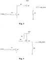
Fig. 3 is a diagram showing the structure of an electronic device including double triodes provided by an embodiment of the present invention; and -
Fig. 4 is a diagram showing the structure of an electronic device including a triode and an MOSFET provided by an embodiment of the present invention. - The basic principle of the present invention includes: a control pin of a control circuit of a device is connected with a VCHG pin of a power management chip; an output pin of the control circuit is connected with a USB_VBUS pin of a USB interface chip; a power pin of the control circuit is connected with a fixed voltage input end which inputs a high level; and the control circuit is configured to output a fixed voltage from its output pin when detecting that the voltage of the control pin is more than a set threshold and output a low level from its output pin when detecting that the voltage of the control pin is less than the set threshold.
- Preferred embodiments of the present invention are described below with reference to the drawings. The first embodiment of the present invention shows an
electronic device 100 with a USB interface, which is described below fundamentally with reference toFig. 2 . Thedevice 100 includes apower management chip 102, aUSB interface chip 103 and acontrol circuit 104, wherein thecontrol circuit 104 is connected with thepower management chip 102 and theUSB interface chip 103 respectively and adopts a charging voltage (VCHG) input to thepower management chip 102 as a control signal to output a voltage corresponding to the control signal to a USB power anode (USB_VBUS) pin of theUSB interface chip 103, wherein the control signal and the voltage output to the USB_VBUS pin are isolated mutually. Specifically, thepower management chip 102, theUSB interface chip 103 and thecontrol circuit 104 are grounded commonly. A charging voltage (VCHG) pin and a grounded pin of thepower management chip 102 are connected with the anode and cathode of anexternal charger 101 respectively; the control pin of thecontrol circuit 104 is connected with the VCHG pin of thepower management chip 102; the output pin of thecontrol circuit 104 is connected with the USB power anode (USB_VBUS) pin of theUSB interface chip 102; the power pin of thecontrol circuit 104 is connected with a fixedvoltage input end 105; the fixedvoltage input end 105 inputs a high level, such as 2.85V, which is more than a starting voltage of a USB status machine, such as 2.0V, and less than the maximum working voltage of the USB_VBUS, such as 5.25V; and thecontrol circuit 104 is configured to output a fixed voltage from its output pin when detecting that the voltage of the control pin is more than a set threshold, such as 3.3V, and output a low level of 0V from its output pin when detecting that the voltage of the control pin is less than the set threshold, 3.3V, wherein the low level should be more than or equal to 0V and less than the starting voltage of the USB status machine. - Based on the circuit, the principle of the method for starting the USB by the VCHG is as follows.
- 1: A control circuit detects the voltage of a control pin.
- 2: The control circuit outputs a fixed high level (ranging from 2.0V to 5.0V, such as 2.85V) from an output pin when detecting that the voltage at the VCHG is more than a threshold and the fixed high level is connected to the USB_VBUS pin. The USB interface chip starts the USB status machine when the USB_VBUS detects the voltage at the USB_VBUS is more than the Session value (such as 2.0V) in the USB specification.
- 3: The control circuit outputs a fixed low level (ranging from 0V to 2.0V, such as 0V) from the output pin when detecting that the voltage at the VCHG is less than or equal to a threshold, and the fixed low level is connected to the USB_VBUS pin. The USB interface chip stops the USB status machine when the USB_VBUS detects the voltage at the USB_VBUS is less than the Session value (such as 2.0V) in the USB specification.
- With reference to
Fig. 3 , the control circuit including an NPN triode and a PNP triode is described below in detail. The control circuit includes: - a first triode Q1, wherein the base of the first triode Q1 is connected with the charging voltage (VCHG) pin of the power management chip through a first resistor R1, the collector of the first triode Q1 is connected with the base of a second triode Q2 through a second resistor R2 and the emitter of the first triode Q1 is grounded; and
- the second triode Q2, wherein the emitter of the second triode Q2 is connected with a fixed voltage output end and the collector of the second triode Q2 is connected with the USB_VBUS pin of the USB interface chip and is grounded through a third resistor R3.
- The role of each component of the control circuit is described as follows. The first resistor R1 and the NPN triode (the first triode Q1) form a charging input voltage detection part, wherein the first resistor R1 is configured to adjust a detection voltage threshold and a maximum input voltage value, namely, adjusting the turn-on voltage threshold of the first triode Q1 and the charging threshold to be almost the same and meet the requirement of overvoltage protection, for example, if the maximum voltage for the overvoltage protection is 10V, the control circuit and other circuits of the terminal may not be damaged when the VCHG is 0-10V. The second resistor R2 and the PNP triode (the second triode Q2) form a control output part, wherein the second resistor R2 is configured to limit current and the second triode Q2 is configured to control output. The fixed
voltage input end 105 is a high-level fixed voltage source VDD, ranging from 2.0V to 5.0V. The third resistor R3 serves as a pull-down resistor to ensure that the output of the second triode Q2 is 0V when the second triode Q2 is off. - Correspondingly, in an embodiment of the present invention provides a method for starting USB communication by VCHG, a control circuit detects a VCHG signal and outputs a voltage corresponding to a control signal to a USB_VBUS pin according to the VCHG signal, specifically including steps as follows.
- Step 1: It is detected whether the charging voltage (VCHG) is more than a threshold (such as 3.3V), if so, Step 2 is executed, otherwise, Step 3 is executed.
- Step 2: The first triode Q1 is on and then the second triode Q2 is on. A fixed high level VDD (such as 2.85V) is added to the USB_VBUS, and if the voltage is more than the Session value, starting the USB communication and returning to Step 1.
- Step 3: The first triode Q1 is off and controls the second triode Q2 to be off, thereby, the voltage 0V generated by the pull-down effect of the third resistor R3 to the ground is added to the USB_VBUS, and if the voltage is less than the Session value, stopping the USB communication and returning to Step 1.
- With reference to
Fig. 4 , the control circuit including an NPN triode and an MOS tube, i.e., an MOSFET, is described in detail. The control circuit includes: - a first triode Q1, wherein the base of the first triode Q1 is connected with the charging voltage (VCHG) pin of a power management chip through a first resistor R1, the collector of the first triode Q1 is connected with the gate of the first MOS tube Q1 through a fourth resistor R4 and the emitter of the first triode Q1 is grounded; and
- the first MOS tube Q3, wherein the drain of the first MOS tube Q3 is connected with a fixed voltage output end, the source of the first MOS tube Q3 is connected with the USB_VBUS pin of the USB interface chip and is grounded through a third resistor R3, and the drain of the first MOS tube Q3 is connected with the gate of the first MOS tube Q3 through a fifth resistor R5.
- The role of each component of the circuit is described as follows. The first resistor R1 and the NPN triode (the first triode Q1) form a charging input voltage detection part, wherein the first resistor R1 is configured to adjust a detection voltage threshold and a maximum input voltage value, namely, adjusting the turn-on voltage threshold and the charging threshold of the first triode Q1 to be almost the same and meet the requirement of overvoltage protection, for example, if the maximum voltage for the overvoltage protection is 10V, the control circuit and other circuits of the terminal may not be damaged when the VCHG is 0-10V. The second resistor R2, the fourth resistor R4 and the MOS tube Q3 form a control output part, wherein the second resistor R2 is configured to limit current and the MOS tube Q3 is configured to control output. The fifth resistor R5 serves as a pull-up resistor to ensure that the MOS tube Q3 is also off when the first triode Q1 is off. The fixed
voltage input end 105 is a high-level fixed voltage source VDD, ranging from 2.0V to 5.0V. The third resistor R3 serves as a pull-down resistor to ensure that the output of the MOS tube Q3 is 0V when the MOS tube Q3 is off. A P-type MOS tube is adopted in the embodiment. - Correspondingly, the method for starting USB communication by the VCHG provided by the embodiment of the present invention includes the following steps.
- Step 4: It is detected whether the charging voltage (VCHG) is more than a threshold (such as 3.3V), if so, Step 5 is executed, otherwise, Step 6 is executed.
- Step 5: The first triode Q1 is on and then the MOS tube Q3 is on. A fixed high level VDD (such as 2.85V) is added to the USB_VBUS, and if the voltage is more than the Session value, starting the USB communication and returning to Step 4.
- Step 6: The first triode Q1 is off and controls the MOS tube Q3 to be off, thereby, the voltage 0V generated by the pull-down effect of the third resistor R3 to the ground is added to the USB_VBUS, and if the voltage is less than the Session value, stopping the USB communication and returning to Step 4.
- Finally, it should be explained that the embodiments above are only intended to describe the technical solution of the present invention instead of limiting the present invention. Although the present invention is described in detail with reference to the preferred embodiments, those skilled in the art shall understand that any modifications or equivalent replacements can still be made for the technical solution of the present invention, and the modified technical solution is still within the scope of the technical solution of the present invention even subjected to these modifications or equivalent replacements.
Claims (10)
- An electronic device (100) with a Universal Serial Bus (USB) interface, comprising a power management chip (102), a USB interface chip (103) and a control circuit (104), wherein the control circuit (104) is connected with the power management chip (102) and the USB interface chip (103) respectively and the control circuit (104) being configured to adopt a charging voltage (VCHG) as a control signal to output a voltage corresponding to the control signal to a USB power anode (USB_VBUS) pin of the USB interface chip (103), wherein the charging voltage (VCHG) is connected to an input of the power management chip, wherein the control signal and the voltage output to the USB_VBUS pin are mutually isolated; and characterized in that a control pin of the control circuit (104) is connected with a charging voltage (VCHG) pin of the power management chip (102); an output pin of the control circuit (104) is connected with the USB_VBUS pin of the USB interface chip (103); a power pin of the control circuit (104) is connected with a fixed voltage input end; the fixed voltage input end being configured to input a high level which is more than a starting voltage of a USB status machine and less than a maximum working voltage of the USB_VBUS; the control circuit (104) is configured to output a fixed voltage from the output pin of the control circuit (104) when detecting that the voltage at the control pin is more than a set threshold, and is configured to output a low level from the output pin of the control circuit (104) when detecting that the voltage at the control pin is less than the set threshold, wherein the low level is more than or equal to 0V and less than the starting voltage of the USB status machine.
- The electronic device (100) with the USB interface according to claim 1, characterized in that the control circuit (104) further comprises a first triode (Q1) and a second triode (Q2), wherein
the base of the first triode (Q1) is connected with a charging voltage (VCHG) pin of the power management chip (102), the collector of the first triode (Q1) is connected with the base of the second triode (Q2), and the emitter of the first triode (Q1) is grounded; and
the emitter of the second triode (Q2) is connected with a fixed voltage output end, and the collector of the second triode (Q2) is connected with the USB_VBUS pin of the USB interface chip (103) and is grounded through a third resistor (R3). - The electronic device (100) with the USB interface according to claim 2, characterized in that the base of the first triode (Q1) is connected with the charging voltage (VCHG) pin of the power management chip (102) through a first resistor (R1).
- The electronic device (100) with the USB interface according to claim 2, characterized in that the collector of the first triode (Q1) is connected with the base of the second triode (Q2) through a second resistor (R2).
- The electronic device (100) with the USB interface according to claim 2, characterized in that the first triode (Q1) is a Negative-Positive-Negative, NPN, triode and the second triode (Q2) is a Positive-Negative-Positive, PNP, triode.
- The electronic device (100) with the USB interface according to claim 1, characterized in that the control circuit (104) further comprises a first triode (Q1) and a first Metal-Oxide-Semiconductor Field Effect Transistor, MOSFET, wherein
the base of the first triode (Q1) is connected with a charging voltage (VCHG) pin of the power management chip (102), the collector of the first triode (Q1) is connected with the gate of the first MOSFET, and the emitter of the first triode (Q1) is grounded; and
the drain of the first MOSFET is connected with a fixed voltage output end, the source of the first MOSFET is connected with the USB_VBUS pin of the USB interface chip (103) and is grounded through a third resistor (R3), and the drain of the first MOSFET is connected with the gate of the first MOSFET through a fifth resistor. - The electronic device (100) with the USB interface according to claim 6, characterized in that the base of the first triode (Q1) is connected with the charging voltage (VCHG) pin of the power management chip (102) through a first resistor (R1).
- The electronic device (100) with the USB interface according to claim 6, characterized in that the collector of the first triode (Q1) is connected with the gate of the first MOSFET through a fourth resistor.
- The electronic device (100) with the USB interface according to claim 6, characterized in that the first triode (Q1) is an NPN triode and the MOSFET is a P-type MOSFET.
- A method for starting USB communication for an electronic device (100) with a USB interface, comprising:detecting, by a control circuit (104), a charging voltage (VCHG) signal; andoutputting, by the control circuit (104), a voltage corresponding to a control signal to a USB power anode (USB_VBUS) pin according to the VCHG signal, wherein the control signal and the voltage output to the USB_VBUS pin are mutually isolated; charaterized in that detecting, by the control circuit (104), the VCHG signal comprises: detecting, by the control circuit (104), the voltage of a control pin; andoutputting, by the control circuit (104), the voltage corresponding to the control signal to the USB_VBUS pin according to the VCHG signal comprises: outputting a fixed voltage from an output pin when the control circuit (104) detects that the voltage of the control pin is more than a set threshold, and starting, by a USB interface chip (103), USB communication according to the fixed voltage input from the USB_VBUS pin; andoutputting a low level from the output pin when the control circuit (104) detects that the voltage of the control pin is less than the set threshold, wherein the low level is more than 0V and less than a starting voltage of a USB status machine, and stopping, by the USB interface chip (103), USB communication according to the low level input from the USB_VBUS pin.
Applications Claiming Priority (2)
| Application Number | Priority Date | Filing Date | Title |
|---|---|---|---|
| CN201110102737.0A CN102202117B (en) | 2011-04-22 | 2011-04-22 | Electronic device with USB (universal serial bus) interface and USB communication starting method thereof |
| PCT/CN2011/082563 WO2012142832A1 (en) | 2011-04-22 | 2011-11-21 | Electronic device having usb interface and usb communication start method thereof |
Publications (3)
| Publication Number | Publication Date |
|---|---|
| EP2698969A1 EP2698969A1 (en) | 2014-02-19 |
| EP2698969A4 EP2698969A4 (en) | 2014-09-17 |
| EP2698969B1 true EP2698969B1 (en) | 2018-06-20 |
Family
ID=44662501
Family Applications (1)
| Application Number | Title | Priority Date | Filing Date |
|---|---|---|---|
| EP11863861.8A Not-in-force EP2698969B1 (en) | 2011-04-22 | 2011-11-21 | Electronic device having usb interface and usb communication start method thereof |
Country Status (5)
| Country | Link |
|---|---|
| US (1) | US9201832B2 (en) |
| EP (1) | EP2698969B1 (en) |
| JP (1) | JP5941135B2 (en) |
| CN (1) | CN102202117B (en) |
| WO (1) | WO2012142832A1 (en) |
Families Citing this family (35)
| Publication number | Priority date | Publication date | Assignee | Title |
|---|---|---|---|---|
| CN102202117B (en) | 2011-04-22 | 2015-01-28 | 中兴通讯股份有限公司 | Electronic device with USB (universal serial bus) interface and USB communication starting method thereof |
| CN102223439B (en) | 2011-04-29 | 2014-09-17 | 中兴通讯股份有限公司 | Electronic equipment with USB interface and USB communication starting method thereof |
| CN103064489B (en) | 2011-10-21 | 2016-03-30 | 华为终端有限公司 | A kind of method and terminal of carrying out internal circuit selection according to USB interface state |
| CN103972955B (en) * | 2014-03-24 | 2016-05-25 | 西安乾易企业管理咨询有限公司 | The power supply adaptor of a kind of USB interface charging handshake method and quickly-chargeable |
| CN105701425B (en) * | 2014-11-28 | 2020-04-28 | 鸿富锦精密工业(武汉)有限公司 | Electronic equipment and mainboard and protection circuit thereof |
| CN104993532A (en) * | 2015-06-29 | 2015-10-21 | 袁玮骏 | Cup-shaped charger |
| CN104953661A (en) * | 2015-06-29 | 2015-09-30 | 袁玮骏 | Cup-shaped vehicle-mounted charging connection fixing device |
| CN106650512B (en) * | 2015-07-30 | 2019-09-24 | 联想(北京)有限公司 | A kind of method and electronic equipment for protecting electronic equipment |
| CN105068959A (en) * | 2015-08-25 | 2015-11-18 | 广东欧珀移动通信有限公司 | A charging method and device for a terminal and a terminal with a data exchange function |
| CN106532154B (en) * | 2016-12-20 | 2023-03-21 | 深圳市优迈德科技有限公司 | Novel lithium battery power supply management circuit |
| JP2018116648A (en) * | 2017-01-20 | 2018-07-26 | キヤノン株式会社 | Information processing apparatus, control method thereof, and program |
| FR3063843B1 (en) * | 2017-03-08 | 2019-03-15 | Valeo Equipements Electriques Moteur | ELECTRIC DISCHARGE CIRCUIT WITH CAPACITY, ELECTRICAL SYSTEM AND MOTOR VEHICLE COMPRISING SUCH AN ELECTRIC DISCHARGE CIRCUIT |
| CN106855848B (en) * | 2017-03-13 | 2023-05-09 | 和远智能科技股份有限公司 | OTG power supply control system and method |
| CN107247179A (en) * | 2017-05-03 | 2017-10-13 | 北京世纪龙脉科技有限公司 | A kind of voltage detecting circuit of USB device |
| CN106980320B (en) * | 2017-05-18 | 2020-06-19 | 上海思岚科技有限公司 | Robot charging method and device |
| CN108650404B (en) * | 2018-04-08 | 2021-01-22 | 努比亚技术有限公司 | Port starting circuit, device and mobile terminal |
| CN109194317B (en) * | 2018-09-05 | 2022-08-16 | 潍坊歌尔电子有限公司 | Reset circuit and wearable equipment |
| CN110086219B (en) * | 2019-04-12 | 2021-08-06 | 出门问问信息科技有限公司 | a charging base |
| CN110320844B (en) * | 2019-07-22 | 2024-05-10 | 武汉洲际电讯科技股份有限公司 | Multi-channel control circuit for serial bus of single chip microcomputer |
| CN110429688A (en) * | 2019-08-26 | 2019-11-08 | 吉安伊戈尔电气有限公司 | A USB dual-port charger with interlock control |
| CN111192418B (en) * | 2020-02-24 | 2024-11-22 | 福建升腾资讯有限公司 | A terminal-based financial peripheral self-starting circuit |
| CN111708307B (en) * | 2020-06-30 | 2025-03-25 | 深圳数联天下智能科技有限公司 | A transceiver control circuit for a wireless communication module |
| CN111884282B (en) * | 2020-07-10 | 2022-12-16 | 广东小天才科技有限公司 | Quick charging method |
| CN112186842B (en) * | 2020-09-21 | 2023-02-17 | 苏州浩创信息科技有限公司 | Charging and communication circuit and electronic device |
| CN112290640B (en) * | 2020-11-11 | 2022-09-02 | 维沃移动通信有限公司 | Interface circuit and electronic equipment charge |
| CN112806946B (en) * | 2021-01-21 | 2025-02-14 | 中山市微视医用科技有限公司 | An endoscope USB isolation circuit |
| CN112993960B (en) * | 2021-03-05 | 2024-08-16 | 上海有个机器人有限公司 | Power supply bleeder circuit and electronic equipment |
| CN113114188B (en) * | 2021-03-23 | 2023-02-07 | 广州吉欧电子科技有限公司 | USB (Universal Serial bus) plug-in triggering starting circuit and electronic equipment |
| CN113347011B (en) * | 2021-04-20 | 2022-11-15 | 深圳市广和通无线股份有限公司 | Communication device, system and communication method |
| CN113900871A (en) * | 2021-10-08 | 2022-01-07 | 重庆电哥科技(集团)有限公司 | A circuit and method for detecting the insertion of a USB device |
| CN114253191B (en) * | 2021-12-17 | 2024-03-19 | 深圳市莫尼迪科技有限责任公司 | HDMI interface reverse power supply circuit and power supply method |
| CN114039400B (en) * | 2022-01-11 | 2022-06-07 | 荣耀终端有限公司 | Electronic equipment |
| CN117092557A (en) * | 2022-05-19 | 2023-11-21 | 群创光电股份有限公司 | electronic device |
| CN116069702A (en) * | 2023-03-03 | 2023-05-05 | 山东华翼微电子技术股份有限公司 | NFC-based USB on-off controller and system |
| CN117375210B (en) * | 2023-12-07 | 2024-02-20 | 广州通则康威科技股份有限公司 | A power supply circuit suitable for CPE equipment |
Family Cites Families (15)
| Publication number | Priority date | Publication date | Assignee | Title |
|---|---|---|---|---|
| JP2003263245A (en) | 2002-03-07 | 2003-09-19 | Fuji Xerox Co Ltd | Usb device |
| JP4153262B2 (en) * | 2002-08-21 | 2008-09-24 | 富士通株式会社 | Bus power device |
| GB2402819B (en) * | 2003-06-11 | 2005-08-03 | Research In Motion Ltd | Universal serial bus charger for a mobile device |
| EP2562618A3 (en) * | 2004-02-17 | 2013-05-22 | Research In Motion Limited | Method and apparatus for handling a charging state in a mobile electronic device |
| JP4016209B2 (en) * | 2004-03-23 | 2007-12-05 | ソニー株式会社 | Electronics |
| KR20060024673A (en) * | 2004-09-14 | 2006-03-17 | 엘지전자 주식회사 | Portable terminal with universal serial bus terminal and method for driving universal serial bus |
| US7268561B2 (en) * | 2004-09-20 | 2007-09-11 | Texas Instruments Incorporated | USB attach detection for USB 1.1 and USB OTG devices |
| CN101461117B (en) * | 2006-06-02 | 2014-04-23 | 日本电气株式会社 | Electronic device and connector mating method |
| JP2008027147A (en) * | 2006-07-20 | 2008-02-07 | Toshiba Corp | Mobile device |
| KR101343581B1 (en) * | 2007-06-22 | 2013-12-19 | 엘지전자 주식회사 | Mobile terminal and its charging device |
| JP2010020439A (en) * | 2008-07-09 | 2010-01-28 | Nec Corp | System power supply lsi and electronic equipment |
| TW201012024A (en) * | 2008-09-08 | 2010-03-16 | Richtek Technology Corp | Battery system and controlling method thereof and the charger for the battery system |
| CN101674366B (en) * | 2009-09-19 | 2012-03-28 | 惠州Tcl移动通信有限公司 | Mobile terminal USB, or charger inserting identification method and identification device thereof |
| CN101783427B (en) | 2010-01-19 | 2014-06-11 | 中兴通讯股份有限公司 | Intelligent charging method and intelligent charging device of terminal |
| CN102202117B (en) * | 2011-04-22 | 2015-01-28 | 中兴通讯股份有限公司 | Electronic device with USB (universal serial bus) interface and USB communication starting method thereof |
-
2011
- 2011-04-22 CN CN201110102737.0A patent/CN102202117B/en not_active Expired - Fee Related
- 2011-11-21 US US14/113,238 patent/US9201832B2/en not_active Expired - Fee Related
- 2011-11-21 WO PCT/CN2011/082563 patent/WO2012142832A1/en not_active Ceased
- 2011-11-21 JP JP2014505488A patent/JP5941135B2/en not_active Expired - Fee Related
- 2011-11-21 EP EP11863861.8A patent/EP2698969B1/en not_active Not-in-force
Non-Patent Citations (1)
| Title |
|---|
| None * |
Also Published As
| Publication number | Publication date |
|---|---|
| CN102202117B (en) | 2015-01-28 |
| JP2014512769A (en) | 2014-05-22 |
| US9201832B2 (en) | 2015-12-01 |
| EP2698969A4 (en) | 2014-09-17 |
| CN102202117A (en) | 2011-09-28 |
| EP2698969A1 (en) | 2014-02-19 |
| WO2012142832A1 (en) | 2012-10-26 |
| US20140051479A1 (en) | 2014-02-20 |
| JP5941135B2 (en) | 2016-06-29 |
Similar Documents
| Publication | Publication Date | Title |
|---|---|---|
| US9201832B2 (en) | Electronic device with USB interface and method for starting USB communication therefor | |
| US10658860B2 (en) | Electronic device, charger within the electronic device, and detecting method for detecting abnormal status of connector of electronic device | |
| US10181742B2 (en) | Electronic device, charger within the electronic device, and detecting method for detecting abnormal status of connector of electronic device | |
| CN101174770B (en) | Charging protection device | |
| US11545824B2 (en) | USB short circuit protection | |
| CN102223439B (en) | Electronic equipment with USB interface and USB communication starting method thereof | |
| CN103208822A (en) | Universal serial bus (USB) charging control circuit | |
| US20190207385A1 (en) | Overvoltage Protection Apparatus and Method | |
| CN111525630B (en) | Charging control device and charging control method | |
| CN106249830B (en) | Electric energy transmission system and method | |
| CN106104994A (en) | A kind of DC D/C power and low pressure thereof switch off control circuit | |
| TWI812013B (en) | Over voltage protection circuit for usb type-c port and related method | |
| US20130300213A1 (en) | Identification circuit | |
| US10817450B1 (en) | USB apparatus and operation method thereof | |
| CN104678197A (en) | Test circuit | |
| CN106160038B (en) | Charging circuit | |
| CN216649235U (en) | HDMI port protection circuit and HDMI port protection device | |
| CN112017579B (en) | Display device and driving system thereof | |
| TWI709300B (en) | Overvoltage protection circuit and method thereof | |
| CN212909054U (en) | Output voltage protection circuit for charger | |
| CN101986492B (en) | Short-circuit protection circuit and short-circuit protection method | |
| US8796890B2 (en) | Power control module | |
| CN207977732U (en) | A kind of self cut-off protection circuit of detection DC-DC power source output voltage | |
| CN104330998B (en) | The portable terminal and its method of Auto Power On under overvoltage condition can be prevented | |
| CN114172140B (en) | Electrostatic protection circuit, circuit board assembly and liquid crystal display device |
Legal Events
| Date | Code | Title | Description |
|---|---|---|---|
| PUAI | Public reference made under article 153(3) epc to a published international application that has entered the european phase |
Free format text: ORIGINAL CODE: 0009012 |
|
| 17P | Request for examination filed |
Effective date: 20131114 |
|
| AK | Designated contracting states |
Kind code of ref document: A1 Designated state(s): AL AT BE BG CH CY CZ DE DK EE ES FI FR GB GR HR HU IE IS IT LI LT LU LV MC MK MT NL NO PL PT RO RS SE SI SK SM TR |
|
| DAX | Request for extension of the european patent (deleted) | ||
| A4 | Supplementary search report drawn up and despatched |
Effective date: 20140819 |
|
| RIC1 | Information provided on ipc code assigned before grant |
Ipc: H02J 7/00 20060101ALN20140812BHEP Ipc: G06F 1/26 20060101AFI20140812BHEP |
|
| STAA | Information on the status of an ep patent application or granted ep patent |
Free format text: STATUS: EXAMINATION IS IN PROGRESS |
|
| 17Q | First examination report despatched |
Effective date: 20170321 |
|
| REG | Reference to a national code |
Ref country code: DE Ref legal event code: R079 Ref document number: 602011049478 Country of ref document: DE Free format text: PREVIOUS MAIN CLASS: H04M0001020000 Ipc: G06F0001260000 |
|
| GRAP | Despatch of communication of intention to grant a patent |
Free format text: ORIGINAL CODE: EPIDOSNIGR1 |
|
| RIC1 | Information provided on ipc code assigned before grant |
Ipc: G06F 1/26 20060101AFI20171130BHEP Ipc: H02J 7/00 20060101ALN20171130BHEP |
|
| STAA | Information on the status of an ep patent application or granted ep patent |
Free format text: STATUS: GRANT OF PATENT IS INTENDED |
|
| INTG | Intention to grant announced |
Effective date: 20180104 |
|
| GRAS | Grant fee paid |
Free format text: ORIGINAL CODE: EPIDOSNIGR3 |
|
| GRAA | (expected) grant |
Free format text: ORIGINAL CODE: 0009210 |
|
| STAA | Information on the status of an ep patent application or granted ep patent |
Free format text: STATUS: THE PATENT HAS BEEN GRANTED |
|
| AK | Designated contracting states |
Kind code of ref document: B1 Designated state(s): AL AT BE BG CH CY CZ DE DK EE ES FI FR GB GR HR HU IE IS IT LI LT LU LV MC MK MT NL NO PL PT RO RS SE SI SK SM TR |
|
| REG | Reference to a national code |
Ref country code: GB Ref legal event code: FG4D |
|
| REG | Reference to a national code |
Ref country code: IE Ref legal event code: FG4D |
|
| REG | Reference to a national code |
Ref country code: AT Ref legal event code: REF Ref document number: 1011054 Country of ref document: AT Kind code of ref document: T Effective date: 20180715 |
|
| REG | Reference to a national code |
Ref country code: DE Ref legal event code: R096 Ref document number: 602011049478 Country of ref document: DE |
|
| REG | Reference to a national code |
Ref country code: NL Ref legal event code: MP Effective date: 20180620 |
|
| PG25 | Lapsed in a contracting state [announced via postgrant information from national office to epo] |
Ref country code: SE Free format text: LAPSE BECAUSE OF FAILURE TO SUBMIT A TRANSLATION OF THE DESCRIPTION OR TO PAY THE FEE WITHIN THE PRESCRIBED TIME-LIMIT Effective date: 20180620 Ref country code: LT Free format text: LAPSE BECAUSE OF FAILURE TO SUBMIT A TRANSLATION OF THE DESCRIPTION OR TO PAY THE FEE WITHIN THE PRESCRIBED TIME-LIMIT Effective date: 20180620 Ref country code: BG Free format text: LAPSE BECAUSE OF FAILURE TO SUBMIT A TRANSLATION OF THE DESCRIPTION OR TO PAY THE FEE WITHIN THE PRESCRIBED TIME-LIMIT Effective date: 20180920 Ref country code: NO Free format text: LAPSE BECAUSE OF FAILURE TO SUBMIT A TRANSLATION OF THE DESCRIPTION OR TO PAY THE FEE WITHIN THE PRESCRIBED TIME-LIMIT Effective date: 20180920 Ref country code: FI Free format text: LAPSE BECAUSE OF FAILURE TO SUBMIT A TRANSLATION OF THE DESCRIPTION OR TO PAY THE FEE WITHIN THE PRESCRIBED TIME-LIMIT Effective date: 20180620 |
|
| REG | Reference to a national code |
Ref country code: LT Ref legal event code: MG4D |
|
| PG25 | Lapsed in a contracting state [announced via postgrant information from national office to epo] |
Ref country code: GR Free format text: LAPSE BECAUSE OF FAILURE TO SUBMIT A TRANSLATION OF THE DESCRIPTION OR TO PAY THE FEE WITHIN THE PRESCRIBED TIME-LIMIT Effective date: 20180921 Ref country code: RS Free format text: LAPSE BECAUSE OF FAILURE TO SUBMIT A TRANSLATION OF THE DESCRIPTION OR TO PAY THE FEE WITHIN THE PRESCRIBED TIME-LIMIT Effective date: 20180620 Ref country code: LV Free format text: LAPSE BECAUSE OF FAILURE TO SUBMIT A TRANSLATION OF THE DESCRIPTION OR TO PAY THE FEE WITHIN THE PRESCRIBED TIME-LIMIT Effective date: 20180620 Ref country code: HR Free format text: LAPSE BECAUSE OF FAILURE TO SUBMIT A TRANSLATION OF THE DESCRIPTION OR TO PAY THE FEE WITHIN THE PRESCRIBED TIME-LIMIT Effective date: 20180620 |
|
| REG | Reference to a national code |
Ref country code: AT Ref legal event code: MK05 Ref document number: 1011054 Country of ref document: AT Kind code of ref document: T Effective date: 20180620 |
|
| PG25 | Lapsed in a contracting state [announced via postgrant information from national office to epo] |
Ref country code: NL Free format text: LAPSE BECAUSE OF FAILURE TO SUBMIT A TRANSLATION OF THE DESCRIPTION OR TO PAY THE FEE WITHIN THE PRESCRIBED TIME-LIMIT Effective date: 20180620 |
|
| PG25 | Lapsed in a contracting state [announced via postgrant information from national office to epo] |
Ref country code: PL Free format text: LAPSE BECAUSE OF FAILURE TO SUBMIT A TRANSLATION OF THE DESCRIPTION OR TO PAY THE FEE WITHIN THE PRESCRIBED TIME-LIMIT Effective date: 20180620 Ref country code: SK Free format text: LAPSE BECAUSE OF FAILURE TO SUBMIT A TRANSLATION OF THE DESCRIPTION OR TO PAY THE FEE WITHIN THE PRESCRIBED TIME-LIMIT Effective date: 20180620 Ref country code: AT Free format text: LAPSE BECAUSE OF FAILURE TO SUBMIT A TRANSLATION OF THE DESCRIPTION OR TO PAY THE FEE WITHIN THE PRESCRIBED TIME-LIMIT Effective date: 20180620 Ref country code: IS Free format text: LAPSE BECAUSE OF FAILURE TO SUBMIT A TRANSLATION OF THE DESCRIPTION OR TO PAY THE FEE WITHIN THE PRESCRIBED TIME-LIMIT Effective date: 20181020 Ref country code: CZ Free format text: LAPSE BECAUSE OF FAILURE TO SUBMIT A TRANSLATION OF THE DESCRIPTION OR TO PAY THE FEE WITHIN THE PRESCRIBED TIME-LIMIT Effective date: 20180620 Ref country code: RO Free format text: LAPSE BECAUSE OF FAILURE TO SUBMIT A TRANSLATION OF THE DESCRIPTION OR TO PAY THE FEE WITHIN THE PRESCRIBED TIME-LIMIT Effective date: 20180620 Ref country code: EE Free format text: LAPSE BECAUSE OF FAILURE TO SUBMIT A TRANSLATION OF THE DESCRIPTION OR TO PAY THE FEE WITHIN THE PRESCRIBED TIME-LIMIT Effective date: 20180620 |
|
| PG25 | Lapsed in a contracting state [announced via postgrant information from national office to epo] |
Ref country code: ES Free format text: LAPSE BECAUSE OF FAILURE TO SUBMIT A TRANSLATION OF THE DESCRIPTION OR TO PAY THE FEE WITHIN THE PRESCRIBED TIME-LIMIT Effective date: 20180620 Ref country code: SM Free format text: LAPSE BECAUSE OF FAILURE TO SUBMIT A TRANSLATION OF THE DESCRIPTION OR TO PAY THE FEE WITHIN THE PRESCRIBED TIME-LIMIT Effective date: 20180620 Ref country code: IT Free format text: LAPSE BECAUSE OF FAILURE TO SUBMIT A TRANSLATION OF THE DESCRIPTION OR TO PAY THE FEE WITHIN THE PRESCRIBED TIME-LIMIT Effective date: 20180620 |
|
| REG | Reference to a national code |
Ref country code: DE Ref legal event code: R097 Ref document number: 602011049478 Country of ref document: DE |
|
| PLBE | No opposition filed within time limit |
Free format text: ORIGINAL CODE: 0009261 |
|
| STAA | Information on the status of an ep patent application or granted ep patent |
Free format text: STATUS: NO OPPOSITION FILED WITHIN TIME LIMIT |
|
| 26N | No opposition filed |
Effective date: 20190321 |
|
| PG25 | Lapsed in a contracting state [announced via postgrant information from national office to epo] |
Ref country code: DK Free format text: LAPSE BECAUSE OF FAILURE TO SUBMIT A TRANSLATION OF THE DESCRIPTION OR TO PAY THE FEE WITHIN THE PRESCRIBED TIME-LIMIT Effective date: 20180620 |
|
| REG | Reference to a national code |
Ref country code: CH Ref legal event code: PL |
|
| PG25 | Lapsed in a contracting state [announced via postgrant information from national office to epo] |
Ref country code: MC Free format text: LAPSE BECAUSE OF FAILURE TO SUBMIT A TRANSLATION OF THE DESCRIPTION OR TO PAY THE FEE WITHIN THE PRESCRIBED TIME-LIMIT Effective date: 20180620 Ref country code: LU Free format text: LAPSE BECAUSE OF NON-PAYMENT OF DUE FEES Effective date: 20181121 |
|
| REG | Reference to a national code |
Ref country code: BE Ref legal event code: MM Effective date: 20181130 |
|
| REG | Reference to a national code |
Ref country code: IE Ref legal event code: MM4A |
|
| PG25 | Lapsed in a contracting state [announced via postgrant information from national office to epo] |
Ref country code: SI Free format text: LAPSE BECAUSE OF FAILURE TO SUBMIT A TRANSLATION OF THE DESCRIPTION OR TO PAY THE FEE WITHIN THE PRESCRIBED TIME-LIMIT Effective date: 20180620 Ref country code: LI Free format text: LAPSE BECAUSE OF NON-PAYMENT OF DUE FEES Effective date: 20181130 Ref country code: CH Free format text: LAPSE BECAUSE OF NON-PAYMENT OF DUE FEES Effective date: 20181130 |
|
| PG25 | Lapsed in a contracting state [announced via postgrant information from national office to epo] |
Ref country code: IE Free format text: LAPSE BECAUSE OF NON-PAYMENT OF DUE FEES Effective date: 20181121 |
|
| PG25 | Lapsed in a contracting state [announced via postgrant information from national office to epo] |
Ref country code: BE Free format text: LAPSE BECAUSE OF NON-PAYMENT OF DUE FEES Effective date: 20181130 Ref country code: AL Free format text: LAPSE BECAUSE OF FAILURE TO SUBMIT A TRANSLATION OF THE DESCRIPTION OR TO PAY THE FEE WITHIN THE PRESCRIBED TIME-LIMIT Effective date: 20180620 |
|
| PG25 | Lapsed in a contracting state [announced via postgrant information from national office to epo] |
Ref country code: MT Free format text: LAPSE BECAUSE OF NON-PAYMENT OF DUE FEES Effective date: 20181121 |
|
| PG25 | Lapsed in a contracting state [announced via postgrant information from national office to epo] |
Ref country code: TR Free format text: LAPSE BECAUSE OF FAILURE TO SUBMIT A TRANSLATION OF THE DESCRIPTION OR TO PAY THE FEE WITHIN THE PRESCRIBED TIME-LIMIT Effective date: 20180620 |
|
| PGFP | Annual fee paid to national office [announced via postgrant information from national office to epo] |
Ref country code: DE Payment date: 20200107 Year of fee payment: 9 Ref country code: GB Payment date: 20200113 Year of fee payment: 9 |
|
| PG25 | Lapsed in a contracting state [announced via postgrant information from national office to epo] |
Ref country code: PT Free format text: LAPSE BECAUSE OF FAILURE TO SUBMIT A TRANSLATION OF THE DESCRIPTION OR TO PAY THE FEE WITHIN THE PRESCRIBED TIME-LIMIT Effective date: 20180620 |
|
| PG25 | Lapsed in a contracting state [announced via postgrant information from national office to epo] |
Ref country code: MK Free format text: LAPSE BECAUSE OF NON-PAYMENT OF DUE FEES Effective date: 20180620 Ref country code: CY Free format text: LAPSE BECAUSE OF FAILURE TO SUBMIT A TRANSLATION OF THE DESCRIPTION OR TO PAY THE FEE WITHIN THE PRESCRIBED TIME-LIMIT Effective date: 20180620 Ref country code: HU Free format text: LAPSE BECAUSE OF FAILURE TO SUBMIT A TRANSLATION OF THE DESCRIPTION OR TO PAY THE FEE WITHIN THE PRESCRIBED TIME-LIMIT; INVALID AB INITIO Effective date: 20111121 |
|
| PGFP | Annual fee paid to national office [announced via postgrant information from national office to epo] |
Ref country code: FR Payment date: 20200113 Year of fee payment: 9 |
|
| REG | Reference to a national code |
Ref country code: DE Ref legal event code: R119 Ref document number: 602011049478 Country of ref document: DE |
|
| GBPC | Gb: european patent ceased through non-payment of renewal fee |
Effective date: 20201121 |
|
| PG25 | Lapsed in a contracting state [announced via postgrant information from national office to epo] |
Ref country code: FR Free format text: LAPSE BECAUSE OF NON-PAYMENT OF DUE FEES Effective date: 20201130 |
|
| PG25 | Lapsed in a contracting state [announced via postgrant information from national office to epo] |
Ref country code: DE Free format text: LAPSE BECAUSE OF NON-PAYMENT OF DUE FEES Effective date: 20210601 Ref country code: GB Free format text: LAPSE BECAUSE OF NON-PAYMENT OF DUE FEES Effective date: 20201121 |