EP2698959A1 - Method for modulating navigation signal - Google Patents
Method for modulating navigation signal Download PDFInfo
- Publication number
- EP2698959A1 EP2698959A1 EP12771513.4A EP12771513A EP2698959A1 EP 2698959 A1 EP2698959 A1 EP 2698959A1 EP 12771513 A EP12771513 A EP 12771513A EP 2698959 A1 EP2698959 A1 EP 2698959A1
- Authority
- EP
- European Patent Office
- Prior art keywords
- branch
- signal
- multiplier
- pseudo
- baseband
- Prior art date
- Legal status (The legal status is an assumption and is not a legal conclusion. Google has not performed a legal analysis and makes no representation as to the accuracy of the status listed.)
- Granted
Links
Images




Classifications
-
- H—ELECTRICITY
- H04—ELECTRIC COMMUNICATION TECHNIQUE
- H04L—TRANSMISSION OF DIGITAL INFORMATION, e.g. TELEGRAPHIC COMMUNICATION
- H04L27/00—Modulated-carrier systems
- H04L27/32—Carrier systems characterised by combinations of two or more of the types covered by groups H04L27/02, H04L27/10, H04L27/18 or H04L27/26
-
- G—PHYSICS
- G01—MEASURING; TESTING
- G01S—RADIO DIRECTION-FINDING; RADIO NAVIGATION; DETERMINING DISTANCE OR VELOCITY BY USE OF RADIO WAVES; LOCATING OR PRESENCE-DETECTING BY USE OF THE REFLECTION OR RERADIATION OF RADIO WAVES; ANALOGOUS ARRANGEMENTS USING OTHER WAVES
- G01S19/00—Satellite radio beacon positioning systems; Determining position, velocity or attitude using signals transmitted by such systems
- G01S19/01—Satellite radio beacon positioning systems transmitting time-stamped messages, e.g. GPS [Global Positioning System], GLONASS [Global Orbiting Navigation Satellite System] or GALILEO
- G01S19/02—Details of the space or ground control segments
-
- G—PHYSICS
- G01—MEASURING; TESTING
- G01S—RADIO DIRECTION-FINDING; RADIO NAVIGATION; DETERMINING DISTANCE OR VELOCITY BY USE OF RADIO WAVES; LOCATING OR PRESENCE-DETECTING BY USE OF THE REFLECTION OR RERADIATION OF RADIO WAVES; ANALOGOUS ARRANGEMENTS USING OTHER WAVES
- G01S19/00—Satellite radio beacon positioning systems; Determining position, velocity or attitude using signals transmitted by such systems
- G01S19/01—Satellite radio beacon positioning systems transmitting time-stamped messages, e.g. GPS [Global Positioning System], GLONASS [Global Orbiting Navigation Satellite System] or GALILEO
- G01S19/13—Receivers
- G01S19/35—Constructional details or hardware or software details of the signal processing chain
- G01S19/37—Hardware or software details of the signal processing chain
-
- H—ELECTRICITY
- H03—ELECTRONIC CIRCUITRY
- H03D—DEMODULATION OR TRANSFERENCE OF MODULATION FROM ONE CARRIER TO ANOTHER
- H03D3/00—Demodulation of angle-, frequency- or phase- modulated oscillations
- H03D3/26—Demodulation of angle-, frequency- or phase- modulated oscillations by means of sloping amplitude/frequency characteristic of tuned or reactive circuit
-
- H—ELECTRICITY
- H04—ELECTRIC COMMUNICATION TECHNIQUE
- H04L—TRANSMISSION OF DIGITAL INFORMATION, e.g. TELEGRAPHIC COMMUNICATION
- H04L23/00—Apparatus or local circuits for systems other than those covered by groups H04L15/00 - H04L21/00
- H04L23/02—Apparatus or local circuits for systems other than those covered by groups H04L15/00 - H04L21/00 adapted for orthogonal signalling
-
- H—ELECTRICITY
- H04—ELECTRIC COMMUNICATION TECHNIQUE
- H04L—TRANSMISSION OF DIGITAL INFORMATION, e.g. TELEGRAPHIC COMMUNICATION
- H04L25/00—Baseband systems
- H04L25/02—Details ; arrangements for supplying electrical power along data transmission lines
- H04L25/03—Shaping networks in transmitter or receiver, e.g. adaptive shaping networks
-
- H—ELECTRICITY
- H04—ELECTRIC COMMUNICATION TECHNIQUE
- H04L—TRANSMISSION OF DIGITAL INFORMATION, e.g. TELEGRAPHIC COMMUNICATION
- H04L27/00—Modulated-carrier systems
- H04L27/18—Phase-modulated carrier systems, i.e. using phase-shift keying
- H04L27/20—Modulator circuits; Transmitter circuits
-
- H—ELECTRICITY
- H04—ELECTRIC COMMUNICATION TECHNIQUE
- H04B—TRANSMISSION
- H04B2215/00—Reducing interference at the transmission system level
- H04B2215/064—Reduction of clock or synthesizer reference frequency harmonics
- H04B2215/065—Reduction of clock or synthesizer reference frequency harmonics by changing the frequency of clock or reference frequency
Definitions
- the invention relates to the signal system design and signal generation of a satellite navigation system, and more particularly to a method and system for modulating navigation signal with the upper and lower sidebands bearing different services.
- Signal system is the core of a satellite navigation system and it decides the intrinsic performance of the navigation system. If there is any defect in the design of signal system, even though the equipment in ground segment, space segment and user segment is good, there will be also congenital defects in the system performance, thereby disturbing the popularization and application of the navigation system.
- the modulation system is the key in the study of navigation signal system. It decides the power spectrum envelope of navigation signal and is decisive to the key performance indicators of the navigation system like positioning velocity measurement, time service precision, compatibility and interoperability, and capacity of resisting disturbance.
- modulation system design is the biggest concern in this industry.
- signal modulation of satellite navigation has been developed from the first generation of BPSK modulation used by GPS into new modulation systems such as BOC, CBOC, TMBOC, and AltBOC.
- the AltBOC modulation system can bear different services in the upper and lower sidebands, which can not only receive and handle SSB signals independently to achieve the traditional BPSK signal performance, but also realize joint treatment to achieve higher positioning accuracy. Therefore, the AltBOC modulation system has been adopted by the COMPASS global system as the baseline for the modulation system of downgoing signals at the B2 frequency point.
- AltBOC is a quasi BOC modulation system of which the upper and lower sidebands can modulate different pseudo-codes.
- AltBOC was first put forward in 2000, targeting to convey dual line navigation signals using one HPA on E1 and E2 frequency bands. However, owing to the non-constant envelope and signal planning and adjustment at L1 frequency band, AltBOC modulation system is not applied to L1 frequency band.
- CNES put forward the AltBOC modulation system with 4-pseudo-code constant envelope, and was adopted as the modulation mode of navigation signal at GalileoE5a and E5b frequency band.
- AltBOC (15, 10) modulation system whose center frequency is 1,191.795 MHz is adopted.
- the center frequency of a lower sideband is 1,176.45 MHz and that of an upper sideband is 1,207.14 MHz.
- This can not only realize the interoperation with GalileoE5 and GPSL5C signals, but also consider the compatibility with B2 signal in COMPASS district system.
- the AltBOC modulation system put forward by Galileo improves the conversion rate of baseband waveform to 8 times of the subcarrier, improves the level number of subcarrier to 4, and inserts product terms.
- the method and system has the advantages of flexible reception and treatment of signals, high MUX efficiency, and low complexity in signal generation, reception, and treatment.
- a method for modulating navigation signal comprises the following steps:
- step (4) corresponding baseband signal components at Q branch and I branch are looked up in a modulation mapping table according to the current C A , C B , and C P value; a method to establish the modulation mapping table comprises: combining all possible C A , C B and C P values and processing each combination thereof according to steps (41) - (43) to get the baseband signal component at Q branch and I branch corresponding to each combination, and recording each combination and corresponding Q branch component and I branch component thereof to establish the modulation mapping table.
- the invention provides a system for modulating navigation signal according the above-mentioned method.
- the system comprises:
- the invention further provides a system for modulating navigation signal according the above-mentioned method.
- the system comprises:
- the baseband wave form of TD-AltBOC modulating signal is shown in FIG. 5 .
- the baseband signal waveform of TD-AltBOC (15, 10) modulation is shown in FIG. 5 .
- the power spectrum of TD-AltBOC modulating signal comprises two main lobes; wherein, the spectral peak of one main lobe is located at where the carrier frequency is added to the subcarrier frequency; it is mainly the signal component of the upper sideband.
- the spectral peak of the other main lobe is located at where the carrier frequency is subtracted by the subcarrier frequency; it is mainly the signal component of the lower sideband.
- the normalized power spectrum of TD-AltBOC (15, 10) modulating signal is shown in FIG. 6 .
- TD-AltBOC modulating signal possesses favorable flexibility in reception.
- Signal of the upper sideband can be taken as the BPSK (Rc) modulating signal of which the center frequency is equal to the carrier frequency plus subcarrier frequency;
- signal of the lower sideband can be taken as the BPSK (Rc) modulating signal of which the center frequency is equal to the carrier frequency subtracted by subcarrier frequency.
- Signal of the upper and lower sidebands can be respectively received, thereby obtaining the receptivity equivalent to BPSK (Rc); signal of the upper and lower sidebands can also be received jointly, thereby obtaining the receptivity equivalent to BOC (fs, Rc).
- TD-AltBOC modulating signal possesses 100% multiplexing efficiency.
- Adopting time division technique can realize the constant envelope multiplexing of the 4 signal components at the upper and lower sidebands; the product signal component is not introduced, so there is no multiplexing loss.
- the pilot channels of upper and lower sidebands of TD-AltBOC share the same pseudo-code, joint receiving of the double side band is equivalent to cosine BOC modulation, and the number of pseudo-code generator and correlator required by pilot signal track can be halved;
- the conversion rate of TD-AltBOC subcarrier symbol is four times of the subcarrier frequency, while the conversion rate of AltBOC subcarrier symbol is eight times of the subcarrier frequency;
- the baseband processing rate for signal generation is halved;
- the waveform of TD-AltBOC subcarrier is 2 level;
- the waveform of AltBOC subcarrier is 4 level; fewer hardware resources will be consumed by a single correlator during matched receiving; during the time-sharing appearance of data channel and pilot channel of TD-AltBOC modulating signal, some elementary units (such as multiplier) which consume more hardware resources can realize time-sharing multiplexing, thereby improving the resource utilization rate and reducing the consumption of hardware
- the invention combines the TDM mode by chip and 2-signal AltBOC modulation system, which solves the problem in 4-signal constant envelope modulation; it is named as Time Division AltBOC mode, short for TD-AltBOC.
- TD-AltBOC modulation divides the signal transmission time into odd and even time slots.
- the time slot width equals to the pseudo-code chip width.
- the odd time slot transmits the signal component of data channel of the upper and lower sidebands; and, the even time slot transmits the signal component of pilot channel of the upper and lower sidebands.
- the sequential relationship for signal component transmission is shown in FIG. 1 .
- B2b_D refers to the signal component of data channel of the upper sideband
- B2b_P refers to the signal component of pilot channel of the upper sideband
- B2a_D refers to the signal component of data channel of the lower sideband
- B2a_P refers to the signal component of pilot channel of the lower sideband.
- d A ( t ) is the data bit waveform of modulation of data channel of the lower sideband
- c AD (t) is the pseudo-code waveform of data channel of the lower sideband
- c AP (t) is the pseudo-code waveform of data channel of the lower sideband
- d B (t) is the data bit waveform of modulation of data channel of the upper sideband
- c BD (t) is the pseudo-code waveform of data channel of the upper sideband
- c BP (t) is the pseudo-code waveform of data channel of the upper sideband
- SC B cos (
- C AD is the pseudo-code sequence of data channel of the lower sideband (take ⁇ 1);
- C AP is the pseudo-code sequence of pilot channel of the lower sideband;
- C BD is the pseudo-code sequence of data channel of the upper sideband;
- C BP is the pseudo-code sequence of pilot channel of the upper sideband;
- N AD , N AP , N BD and N BP are respectively the code length of C AD , C AP , C AP and C BP ;
- T c is the pseudo-code chip width;
- p ( t ⁇ ) is square topped pulse; sign ( ⁇ ) means the symbolic operation;
- f s is subcarrier frequency (B2 signal is 15 ⁇ 1.023MHz).
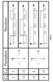
- the planisphere and signal waveform of TD-AltBOC modulating signal are shown in FIG. 4 .
- C A and C B respectively refer to the pseudo-code of lower sideband and upper sideband transmitted in a certain time slot.
- C A d A C AD
- C B d B C BD
- C A C AP
- C B C BP
- the signal waveform depicted in real line is same-phase branch waveform; the signal waveform depicted in dotted line is perpendicular branch waveform.
- the invention adopts the TD-AltBOC programme with the same pseudo-code of pilot channel on the upper and lower sidebands.
- the clock which is 4 times of the subcarrier frequency is taken as the clock signal CLK0 for integrating control generated by TD-AltBOC baseband signal.
- the multipliers 13 and 14 and adder 15 constitute the RF modulator together.
- the invention is not limited to this form. It can also use a special QPSK modulator to realize radio frequency modulation; the number of frequency division of the frequency dividers 17 and 18 is also not restricted to the number of frequency division referred to in the example.
- the number of frequency division of frequency dividers 17 and 18 shall also be changed.
- the number of frequency division of frequency divider 17 is 8*m/n
- the number of frequency division of frequency divider 18 is 4*m/n.
- the baseband clock CLK00 is used as the drive clock of TD-AltBOC modulation.
- Frequency of clock CLK00 is divided by 12 through frequency divider 24 to be the drive clock of pseudo-code generator.
- the pseudo-code generator generates the pseudo-code c BD of data channel of the upper sideband and the pseudo-code c AD of data channel and pseudo-code c P of pilot channel of the lower sideband via half of the code rate Rc; different from the method shown in FIG. 2 , the value of pseudo-code sequence output in this method is selected as 0 or 1, which are respectively corresponding to 1 and -1 in the method shown in FIG. 2 .
- the lower sideband data D A and pseudo-code c AD of data channel of the lower sideband are subject to exclusive-or operation with binary adder 20 to get the compound code C A of the data channel of the lower sideband.
- the upper sideband data D B and pseudo-code c BD of data channel of the upper sideband are subject to exclusive-or operation with binary adder 21 to get the compound code C B of the data channel of the upper sideband.
- the data channel compound code C A of lower sideband, data channel compound code C B of upper sideband and pseudo-code c P of pilot channel of upper sideband are taken as the input of table lookup unit 26 to search the corresponding amplitude sequence of I and Q component, and get the baseband wave form at I branch and baseband wave form at Q branch through pulse modulation.
- the table lookup unit 26 comprises the modulation mapping table comprising a lookup table at I branch and a lookup table at Q branch, which are shown in table 1 and table 2 respectively.
- the baseband wave form at Q branch is used to modulate the sine phase carrier
- baseband wave form at I branch is used to modulate the cosine carrier wave to output TD-AltBOC modulating signal.
- Establishment of table 1 and table 2 is based on the subcarrier modulation theory in FIG. 2 , that is to say, all the possible C A , C B and C P values are combined, and each combination is subject to subcarrier modulation in the same way, thereby obtaining the baseband signal component at Q branch and at I branch corresponding to each combination; record each combination and its corresponding component at Q branch and at I branch to get the modulation mapping table.
Landscapes
- Engineering & Computer Science (AREA)
- Computer Networks & Wireless Communication (AREA)
- Signal Processing (AREA)
- Radar, Positioning & Navigation (AREA)
- Remote Sensing (AREA)
- Physics & Mathematics (AREA)
- General Physics & Mathematics (AREA)
- Power Engineering (AREA)
- Digital Transmission Methods That Use Modulated Carrier Waves (AREA)
Abstract
Description
- The invention relates to the signal system design and signal generation of a satellite navigation system, and more particularly to a method and system for modulating navigation signal with the upper and lower sidebands bearing different services.
- Signal system is the core of a satellite navigation system and it decides the intrinsic performance of the navigation system. If there is any defect in the design of signal system, even though the equipment in ground segment, space segment and user segment is good, there will be also congenital defects in the system performance, thereby disturbing the popularization and application of the navigation system.
- The modulation system is the key in the study of navigation signal system. It decides the power spectrum envelope of navigation signal and is decisive to the key performance indicators of the navigation system like positioning velocity measurement, time service precision, compatibility and interoperability, and capacity of resisting disturbance. During the process of GPS modernization and Galileo signal design, modulation system design is the biggest concern in this industry. At present, signal modulation of satellite navigation has been developed from the first generation of BPSK modulation used by GPS into new modulation systems such as BOC, CBOC, TMBOC, and AltBOC. The AltBOC modulation system can bear different services in the upper and lower sidebands, which can not only receive and handle SSB signals independently to achieve the traditional BPSK signal performance, but also realize joint treatment to achieve higher positioning accuracy. Therefore, the AltBOC modulation system has been adopted by the COMPASS global system as the baseline for the modulation system of downgoing signals at the B2 frequency point.
- AltBOC is a quasi BOC modulation system of which the upper and lower sidebands can modulate different pseudo-codes. AltBOC was first put forward in 2000, targeting to convey dual line navigation signals using one HPA on E1 and E2 frequency bands. However, owing to the non-constant envelope and signal planning and adjustment at L1 frequency band, AltBOC modulation system is not applied to L1 frequency band. In 2001, CNES put forward the AltBOC modulation system with 4-pseudo-code constant envelope, and was adopted as the modulation mode of navigation signal at GalileoE5a and E5b frequency band.
- In COMPASS system, AltBOC (15, 10) modulation system whose center frequency is 1,191.795 MHz is adopted. The center frequency of a lower sideband is 1,176.45 MHz and that of an upper sideband is 1,207.14 MHz. This can not only realize the interoperation with GalileoE5 and GPSL5C signals, but also consider the compatibility with B2 signal in COMPASS district system. However, in order to achieve the modulation through 4-pseudo-code constant envelope, the AltBOC modulation system put forward by Galileo improves the conversion rate of baseband waveform to 8 times of the subcarrier, improves the level number of subcarrier to 4, and inserts product terms. The increase in baseband conversion rate and level of subcarrier will in no doubt multiply the complexity of signal generation and receiving. Introduction of product terms can reduce the multiplexing efficiency, which, to a certain extent, reduces the signal performance. With the smart design, CNES can keep the signal component near the subcarrier frequency not reduced, and ensure the performance of receiver is not damaged even when it only receives the main lobe power. However, the harmonic component of subcarrier can only modulate the useless product signals, so it reduces the performance under broadband receiving conditions.
- In view of the above-described problems, it is one objective of the invention to provide a method and system for modulating navigation signal. The method and system has the advantages of flexible reception and treatment of signals, high MUX efficiency, and low complexity in signal generation, reception, and treatment.
- A method for modulating navigation signal, comprises the following steps:
- 1) dividing frequency of a control clock CLK0 to obtain a pseudo-code generating drive clock CLK1 and a time division multiplexing (TDM) control clock CLK2, where, a frequency of the control clock CLK0 is four times that of a binary subcarrier, a frequency of the pseudo-code generating drive clock CLK1 is 1/2 of a code rate, and a frequency of the TDM control clock CLK2 is equivalent to the code rate;
- 2) driving the CLK1 to generate pseudo-code cBD of a data channel of an upper sideband, pseudo-code cAD of a data channel of a lower sideband, and pseudo-code cP of a pilot channel; driving the CLK0 to generate a binary sine subcarrier SCB,sin and a binary cosine subcarrier SCB,cos;
- 3) modulating the cAD by a lower sideband dA to generate a baseband signal component CA of the data channel of the lower sideband; modulating the cBD by an upper sideband waveform dB to generate a baseband signal component CB of the data channel of the upper sideband;
- 4) modulating the subcarriers, which comprising:
- (41) negating the CA and adding to the CB, and multiplying with the SCB,sin to get a signal component of data channel at Q branch; adding the CA to the CB and multiplying with the SCB,cos to get a signal component of data channel at I branch; multiplying the CP by 2 and then multiplying with the SCB,cos to get a signal component of the pilot channel at I branch;
- (42) when the CLK2 is in a time slot of odd chip, allowing the signal component of the data channel at Q branch to be a signal component of a baseband signal at Q branch, and allowing the signal component of the data channel at I branch to be a signal component of a baseband signal at I branch; when CLK2 is in a time slot of even chip, allowing zero signal to be the signal component of the baseband signal at Q branch, and allowing the signal component of the pilot channel at I branch to be the signal component of the baseband signal at I branch; and
- (5) modulating a sine phase carrier by the signal component of the baseband signal at Q branch, modulating a cosine phase carrier by the signal component of the baseband signal at I branch, and combining the modulation result of the two branches to obtain a modulated radio frequency signal.
- In step (4), corresponding baseband signal components at Q branch and I branch are looked up in a modulation mapping table according to the current CA, CB, and CP value; a method to establish the modulation mapping table comprises: combining all possible CA, CB and CP values and processing each combination thereof according to steps (41) - (43) to get the baseband signal component at Q branch and I branch corresponding to each combination, and recording each combination and corresponding Q branch component and I branch component thereof to establish the modulation mapping table.
- The invention provides a system for modulating navigation signal according the above-mentioned method. The system comprises:
- a
first multiplier 3, afirst subtracter 4, asecond multiplier 7, and a firsttime division multiplexer 11, which are connected in order; - a
fourth multiplier 2, asecond adder 5, a fifth multiplier 8, and a secondtime division multiplexer 12, which are connected in order; - a
seventh multiplier 6 and aneighth multiplier 9 connected in order; - a
pseudo-code generator 1 connected to thefirst multiplier 3, thefourth multiplier 2, and theseventh multiplier 6; - a
first frequency divider 17 connected to thepseudo-code generator 1; - a subcarrier generator connected to the
second multiplier 7, the fifth multiplier 8, and theeighth multiplier 9; - a
second frequency divider 18 connected to the firsttime division multiplexer 11 and the secondtime division multiplexer 12; - the
first multiplier 3 is connected to thesecond adder 5; thefourth multiplier 2 is connected to thefirst subtracter 4; theeighth multiplier 9 is connected to the secondtime division multiplexer 12; the firsttime division multiplexer 11 and secondtime division multiplexer 12 are connected to a RF modulator; the firsttime division multiplexer 11 receives zero signal input. - The invention further provides a system for modulating navigation signal according the above-mentioned method. The system comprises:
- a
frequency divider 24 and apseudo-code generator 19, which are connected; thepseudo-code generator 19 is connected to a first input terminal of abaseband modulation module 26 through a first Exclusive-OR operator 20; thepseudo-code generator 19 is connected to a second input terminal of thebaseband modulation module 26 through a second Exclusive-OR operator 21; thepseudo-code generator 19 is also connected to a third input terminal of thebaseband modulation module 26; the two output terminals of TD-AltBOCbaseband modulation module 26 are connected to a RF modulator. - Advantages of the invention are summarized as follows.
- The time-domain characteristics of TD-AltBOC modulating signal in the invention are as follows: within the odd time slot, the baseband wave form at I and Q branch is decided by the pseudo-code cBD of data channel of the upper sideband and the pseudo-code cAD of data channel of the lower sideband; when CBD = 0 and CAD = 0, the baseband wave form at I branch appears as binary cosine subcarrier, and the baseband wave form at Q branch is 0; when CBD = 1 and CAD = 1, the baseband wave form at I branch appears as reverse binary cosine subcarrier, and the baseband wave form at Q branch is 0; when CBD = 0 and CAD = 1, the baseband wave form at I branch is 0, and the baseband wave form at Q branch appears as binary sine subcarrier; when CBD = 1 and CAD = 0, the baseband wave form at I branch is 0, and the baseband wave form at Q branch appears as reverse binary sine subcarrier. Within the even time slot, the baseband wave form at Q branch is 0, and the baseband wave form at I branch is decided by the pseudo-code CP of pilot channel; when CP = 0, the baseband wave form at I branch appears as binary cosine subcarrier; when CP = 1, the baseband wave form at I branch appears as reverse binary cosine subcarrier. The baseband wave form of TD-AltBOC modulating signal is shown in
FIG. 5 . The baseband signal waveform of TD-AltBOC (15, 10) modulation is shown inFIG. 5 . - The power spectrum of TD-AltBOC modulating signal comprises two main lobes; wherein, the spectral peak of one main lobe is located at where the carrier frequency is added to the subcarrier frequency; it is mainly the signal component of the upper sideband. The spectral peak of the other main lobe is located at where the carrier frequency is subtracted by the subcarrier frequency; it is mainly the signal component of the lower sideband. The normalized power spectrum of TD-AltBOC (15, 10) modulating signal is shown in
FIG. 6 . - TD-AltBOC modulating signal possesses favorable flexibility in reception. Signal of the upper sideband can be taken as the BPSK (Rc) modulating signal of which the center frequency is equal to the carrier frequency plus subcarrier frequency; signal of the lower sideband can be taken as the BPSK (Rc) modulating signal of which the center frequency is equal to the carrier frequency subtracted by subcarrier frequency. Signal of the upper and lower sidebands can be respectively received, thereby obtaining the receptivity equivalent to BPSK (Rc); signal of the upper and lower sidebands can also be received jointly, thereby obtaining the receptivity equivalent to BOC (fs, Rc).
- TD-AltBOC modulating signal possesses 100% multiplexing efficiency. Adopting time division technique can realize the constant envelope multiplexing of the 4 signal components at the upper and lower sidebands; the product signal component is not introduced, so there is no multiplexing loss.
- As for complexity, the pilot channels of upper and lower sidebands of TD-AltBOC share the same pseudo-code, joint receiving of the double side band is equivalent to cosine BOC modulation, and the number of pseudo-code generator and correlator required by pilot signal track can be halved; the conversion rate of TD-AltBOC subcarrier symbol is four times of the subcarrier frequency, while the conversion rate of AltBOC subcarrier symbol is eight times of the subcarrier frequency; the baseband processing rate for signal generation is halved; the waveform of TD-AltBOC subcarrier is 2 level; the waveform of AltBOC subcarrier is 4 level; fewer hardware resources will be consumed by a single correlator during matched receiving; during the time-sharing appearance of data channel and pilot channel of TD-AltBOC modulating signal, some elementary units (such as multiplier) which consume more hardware resources can realize time-sharing multiplexing, thereby improving the resource utilization rate and reducing the consumption of hardware resources. Therefore, the complexity of generation and receiving of TD-AltBOC signal is far below that of AltBOC signal.
-
FIG. 1 shows sequential relationship of transmission of TD-AltBOC signal components; -
FIG. 2 shows a diagram of generation of TD-AltBOC modulating signal; -
FIG. 3 shows the generation of TD-AltBOC modulating signal; and -
FIG. 4 shows planisphere and waveform of TD-AltBOC modulation. - The invention combines the TDM mode by chip and 2-signal AltBOC modulation system, which solves the problem in 4-signal constant envelope modulation; it is named as Time Division AltBOC mode, short for TD-AltBOC.
- Parameter definition of TD-AltBOC (m, n) modulation: m refers to the multiple of f0, the relative reference frequency of subcarrier frequency, namely fs =m×f 0; n refers to the multiple of f0, relative reference frequency of code rate, namely, Rc =n×f 0.
- TD-AltBOC modulation divides the signal transmission time into odd and even time slots. The time slot width equals to the pseudo-code chip width. The odd time slot transmits the signal component of data channel of the upper and lower sidebands; and, the even time slot transmits the signal component of pilot channel of the upper and lower sidebands. The sequential relationship for signal component transmission is shown in
FIG. 1 . - In
FIG. 1 , B2b_D refers to the signal component of data channel of the upper sideband; B2b_P refers to the signal component of pilot channel of the upper sideband; B2a_D refers to the signal component of data channel of the lower sideband; B2a_P refers to the signal component of pilot channel of the lower sideband. - The mathematical representation of TD-AltBOC modulating baseband signal is

wherein, dA (t) is the data bit waveform of modulation of data channel of the lower sideband; cAD(t) is the pseudo-code waveform of data channel of the lower sideband; cAP(t) is the pseudo-code waveform of data channel of the lower sideband; dB(t) is the data bit waveform of modulation of data channel of the upper sideband; cBD(t) is the pseudo-code waveform of data channel of the upper sideband; cBP(t) is the pseudo-code waveform of data channel of the upper sideband; SC B,cos(t) is binary cosine subcarrier; SC B,sin (t) is binary sine subcarrier. They are:


- wherein, CAD is the pseudo-code sequence of data channel of the lower sideband (take ±1); CAP is the pseudo-code sequence of pilot channel of the lower sideband; CBD is the pseudo-code sequence of data channel of the upper sideband; CBP is the pseudo-code sequence of pilot channel of the upper sideband; NAD, NAP, NBD and NBP are respectively the code length of CAD, CAP, CAP and CBP ; Tc is the pseudo-code chip width; p(t̃) is square topped pulse; sign(●) means the symbolic operation; fs is subcarrier frequency (B2 signal is 15×1.023MHz). p(t̃) is defined as follows

- The planisphere and signal waveform of TD-AltBOC modulating signal are shown in
FIG. 4 . - In
FIG. 4 , CA and CB respectively refer to the pseudo-code of lower sideband and upper sideband transmitted in a certain time slot. When the present time slot is odd time slot, CA =dACAD, CB =dBCBD ; when the present time slot is even time slot, CA =CAP, CB =CBP . The signal waveform depicted in real line is same-phase branch waveform; the signal waveform depicted in dotted line is perpendicular branch waveform. - If the upper and lower sidebands adopt the same code sequence, namely CAP=CBP , the expression of TD-AltBOC modulating baseband signal is

- Namely, in even time slot, there will only be binary cosine subcarrier on the same-phase branch.
- If the upper and lower sidebands adopt the reverse code sequence, namely CAP=-CBP, the expression of TD-AltBOC modulating baseband signal is

- Namely, in even time slot, there will only be binary sine subcarrier on the perpendicular branch.
- In order to reduce the complexity in signal reception and processing and optimize the receptivity, the invention adopts the TD-AltBOC programme with the same pseudo-code of pilot channel on the upper and lower sidebands. The mathematical representation is

- When 2fs•Tc is an odd number, the normalized power spectrum of TD-AltBOC signal is

- When 2fs •Tc is an even number, the normalized power spectrum of TD-AltBOC signal is

-
FIG. 2 is an example of TD-AltBOC (15, 10) signal generation of which the reference frequency f0 = 1.023MHz; it contains the following procedures: - The clock which is 4 times of the subcarrier frequency is taken as the clock signal CLK0 for integrating control generated by TD-AltBOC baseband signal.
- 1) The control clock frequency is divided by 12 through the
frequency divider 17 to generate the drive clock CLK1 of pseudo-code generator. - 2) The pseudo-code cBD of data channel of the upper sideband (+1 or -1), pseudo-code cAD of data channel of the lower sideband (+1 or -1) and the pseudo-code cP of pilot channel of the lower sideband (+1 or -1) are generated via half of the code rate Rc.
- 3) The binary NRZ waveform dA of the lower sideband data (1 refers to
data bit 0; -1 refers to data bit 1) is multiplied by pseudo-code cAD of the data channel of the lower sideband through themultiplier 3. - 4) The binary NRZ waveform dB of the upper sideband data (1 refers to
data bit 0; -1 refers to data bit 1) is multiplied by pseudo-code cBD of the data channel of the upper sideband through themultiplier 2. - 5) After reverse sign of the output of
multiplier 3, it is added to the output ofmultiplier 2 through adder 4 (equivalent to subtracter). - 6) The output of
multiplier 3 is added to the output ofmultiplier 2 throughadder 5. - 7) The pseudo-code output of pilot channel of the pseudo-code generator is multiplied by 2 through the
multiplier 6. - 8) CLK0 is used to drive subcarrier generator to generate binary sine subcarrier SCB,sin and binary cosine subcarrier SCB,cos.
- 9) The output of
multiplier 6 is multiplied by binary cosine subcarrier SCB,cos throughmultiplier 9 to get the signal component of pilot channel at I branch; the signal component of pilot channel at Q branch is constantly 0. - 10) The output of
adder 5 is multiplied by binary cosine subcarrier SCB,cos through multiplier 8 to get the signal component of data channel at I branch. - 11) The output of
adder 4 is multiplied by binary sine subcarrier SCB,sin throughmultiplier 7 to get the signal component of data channel at Q branch. - 12) The output of
multiplier time division multiplexer 11. - 13) The output of multiplier 8 and output of
multiplier 9 are taken as the two inputs oftime division multiplexer 12. - 14) Frequency of the baseband clock CLK0 is divided by 6 through the
frequency divider 18 to get the time division multiplexer control clock CLK2. - 15) Under the control of clock CLK2, the
time division multiplexer 11 andtime division multiplexer 12 finish the synchronous switching of data channel and pilot channel; in the odd chip time slot, thetime division multiplexer 11 outputs the signal component of data channel at Q branch, andtime division multiplexer 12 outputs the signal component of data channel at I branch; in the even chip time slot, thetime division multiplexer 11outputs 0, andtime division multiplexer 12 outputs the signal component of pilot channel at I branch; The output oftime division multiplexer 11 is the signal component of resultant signal at Q branch; the output oftime division multiplexer 12 is the signal component of resultant signal at I branch. - 16)
Time division multiplexer 11 is used to output the modulated sine phase carrier of baseband signal at Q branch to get the component of radio-frequency signal at Q branch. - 17)
Time division multiplexer 12 is used to output the modulated cosine phase carrier of baseband signal at Q branch to get the component of radio-frequency signal at I branch. - 18) The component of radio-frequency signal at Q branch and component of radio-frequency signal at I branch are integrated to get TD-AltBOC modulated radio frequency signal.
- In the example, the
multipliers adder 15 constitute the RF modulator together. The invention is not limited to this form. It can also use a special QPSK modulator to realize radio frequency modulation; the number of frequency division of thefrequency dividers frequency dividers frequency divider 17 is 8*m/n, and the number of frequency division offrequency divider 18 is 4*m/n. - As is shown in
FIG. 3 , it includes the following procedures:
1) The baseband clock CLK00 is used as the drive clock of TD-AltBOC modulation.
2) Frequency of clock CLK00 is divided by 12 throughfrequency divider 24 to be the drive clock of pseudo-code generator.
3) The pseudo-code generator generates the pseudo-code cBD of data channel of the upper sideband and the pseudo-code cAD of data channel and pseudo-code cP of pilot channel of the lower sideband via half of the code rate Rc; different from the method shown inFIG. 2 , the value of pseudo-code sequence output in this method is selected as 0 or 1, which are respectively corresponding to 1 and -1 in the method shown inFIG. 2 .
4) The lower sideband data DA and pseudo-code cAD of data channel of the lower sideband are subject to exclusive-or operation withbinary adder 20 to get the compound code CA of the data channel of the lower sideband.
5) The upper sideband data DB and pseudo-code cBD of data channel of the upper sideband are subject to exclusive-or operation withbinary adder 21 to get the compound code CB of the data channel of the upper sideband.
6) The data channel compound code CA of lower sideband, data channel compound code CB of upper sideband and pseudo-code cP of pilot channel of upper sideband are taken as the input oftable lookup unit 26 to search the corresponding amplitude sequence of I and Q component, and get the baseband wave form at I branch and baseband wave form at Q branch through pulse modulation. Thetable lookup unit 26 comprises the modulation mapping table comprising a lookup table at I branch and a lookup table at Q branch, which are shown in table 1 and table 2 respectively.
7) The baseband wave form at Q branch is used to modulate the sine phase carrier, and baseband wave form at I branch is used to modulate the cosine carrier wave to output TD-AltBOC modulating signal.Table 1 Lookup table for I branch Input Output (I) CA CB CP 1 2 3 4 5 6 7 8 9 10 11 12 0 0 0 1 -1 -1 1 1 -1 -1 1 1 -1 -1 1 0 0 1 1 -1 -1 1 1 -1 1 -1 -1 1 1 -1 0 1 0 0 0 0 0 0 0 -1 1 1 -1 -1 1 0 1 1 0 0 0 0 0 0 1 -1 -1 1 1 -1 1 0 0 0 0 0 0 0 0 -1 1 1 -1 -1 1 1 0 1 0 0 0 0 0 0 1 -1 -1 1 1 -1 1 1 0 -1 1 1 -1 -1 1 -1 1 1 -1 -1 1 1 1 1 -1 1 1 -1 -1 1 1 -1 -1 1 1 -1 Table 2 Lookup table for Q branch Input Output (Q) CA CB CP 1 2 3 4 5 6 7 8 9 10 11 12 0 0 0 0 0 0 0 0 0 0 0 0 0 0 0 0 0 1 0 0 0 0 0 0 0 0 0 0 0 0 0 1 0 -1 -1 1 1 -1 -1 0 0 0 0 0 0 0 1 1 -1 -1 1 1 -1 -1 0 0 0 0 0 0 1 0 0 1 1 -1 -1 1 1 0 0 0 0 0 0 1 0 1 1 1 -1 -1 1 1 0 0 0 0 0 0 1 1 0 0 0 0 0 0 0 0 0 0 0 0 0 1 1 1 0 0 0 0 0 0 0 0 0 0 0 0 - Establishment of table 1 and table 2 is based on the subcarrier modulation theory in
FIG. 2 , that is to say, all the possible CA, CB and CP values are combined, and each combination is subject to subcarrier modulation in the same way, thereby obtaining the baseband signal component at Q branch and at I branch corresponding to each combination; record each combination and its corresponding component at Q branch and at I branch to get the modulation mapping table. - Table 1 and table 2 are established based on TD-AltBOC (15, 10) modulation, and it is suitable when fs/Rc = 1.5; under other circumstances, the tables can be established in the following way:
- (1) CA, CB, CP is mapped as cA, cB, cP according to the following rule:

- (2) When n takes 0, 1, ......, 4fs/Rc-1, the output SI at I branch and output SQ at Q branch can be calculated according to the following formula


- When n takes 4fs/Rc, ......, 4fs/Rc-1, the output SI at I branch and output SQ at Q branch can be calculated according to the following formula


Claims (4)
- A method for modulating navigation signal, the method comprising the following steps:1) dividing frequency of a control clock CLK0 to obtain a pseudo-code generating drive clock CLK1 and a time division multiplexing (TDM) control clock CLK2, where, a frequency of the control clock CLK0 is four times that of a binary subcarrier, a frequency of the pseudo-code generating drive clock CLK1 is 1/2 of a code rate, and a frequency of the TDM control clock CLK2 is equivalent to the code rate;2) driving the CLK1 to generate pseudo-code cBD of a data channel of an upper sideband, pseudo-code cAD of a data channel of a lower sideband, and pseudo-code cP of a pilot channel; driving the CLK0 to generate a binary sine subcarrier SCB,sin and a binary cosine subcarrier SCB,cos;3) modulating the cAD by a lower sideband dA to generate a baseband signal component CA of the data channel of the lower sideband; modulating the cBD by an upper sideband waveform dB to generate a baseband signal component CB of the data channel of the upper sideband;4) modulating the subcarriers, which comprising:(41) negating the CA and adding to the CB, and multiplying with the SCB,sin to get a signal component of data channel at Q branch; adding the CA to the CB and multiplying with the SCB,cos to get a signal component of data channel at I branch; multiplying the CP by 2 and then multiplying with the SCB,cos to get a signal component of the pilot channel at I branch; and(42) when the CLK2 is in a time slot of odd chip, allowing the signal component of the data channel at Q branch to be a signal component of a baseband signal at Q branch, and allowing the signal component of the data channel at I branch to be a signal component of a baseband signal at I branch; when CLK2 is in a time slot of even chip, allowing zero signal to be the signal component of the baseband signal at Q branch, and allowing the signal component of the pilot channel at I branch to be the signal component of the baseband signal at I branch; and5) modulating a sine phase carrier by the signal component of the baseband signal at Q branch, modulating a cosine phase carrier by the signal component of the baseband signal at I branch, and combining the modulation result of the two branches to obtain a modulated radio frequency signal.
- The method of claim 1, characterized in that in step (4), corresponding baseband signal components at Q branch and I branch are looked up in a modulation mapping table according to the current CA, CB, and CP value; a method to establish the modulation mapping table comprises: combining all possible CA, CB and CP values and processing each combination thereof according to steps (41) - (43) to get the baseband signal component at Q branch and I branch corresponding to each combination, and recording each combination and corresponding Q branch component and I branch component thereof to establish the modulation mapping table.
- A system for modulating navigation signal according the method of claim 1, the system comprising:a) a first multiplier (3), a first subtracter (4), a second multiplier (7), and a first time division multiplexer (11), which are connected in order;b) a fourth multiplier (2), a second adder (5), a fifth multiplier (8), and a second time division multiplexer (12), which are connected in order;c) a seventh multiplier (6) and an eighth multiplier (9) connected in order;d) a pseudo-code generator (1) connected to the first multiplier (3), the fourth multiplier (2), and the seventh multiplier (6);e) a first frequency divider (17) connected to the pseudo-code generator (1);f) a subcarrier generator connected to the second multiplier (7), the fifth multiplier (8), and the eighth multiplier (9); andg) a second frequency divider (18) connected to the first time division multiplexer (11) and the second time division multiplexer (12);characterized in that
the first multiplier (3) is connected to the second adder (5); the fourth multiplier (2) is connected to the first subtracter (4);
the eighth multiplier (9) is connected to the second time division multiplexer (12);
the first time division multiplexer (11) and second time division multiplexer (12) are connected to a RF modulator; and
the first time division multiplexer (11) receives zero signal input. - A system for modulating navigation signal according the method of claim 2, the system comprising: a frequency divider (24) and a pseudo-code generator (19);
characterized in that
the frequency divider (24) and the pseudo-code generator (19) are connected;
the pseudo-code generator (19) is connected to a first input terminal of a baseband modulation module (26) through a first Exclusive-OR operator (20);
the pseudo-code generator (19) is connected to a second input terminal of the baseband modulation module (26) through a second Exclusive-OR operator (21);
the pseudo-code generator (19) is also connected to a third input terminal of the baseband modulation module (26);
two output terminals of the baseband modulation module (26) are connected to a RF modulator.
Applications Claiming Priority (2)
| Application Number | Priority Date | Filing Date | Title |
|---|---|---|---|
| CN2011100949747A CN102209056B (en) | 2011-04-15 | 2011-04-15 | Navigation signal modulation method |
| PCT/CN2012/073075 WO2012139458A1 (en) | 2011-04-15 | 2012-03-27 | Method for modulating navigation signal |
Publications (3)
| Publication Number | Publication Date |
|---|---|
| EP2698959A1 true EP2698959A1 (en) | 2014-02-19 |
| EP2698959A4 EP2698959A4 (en) | 2014-09-24 |
| EP2698959B1 EP2698959B1 (en) | 2017-09-06 |
Family
ID=44697724
Family Applications (1)
| Application Number | Title | Priority Date | Filing Date |
|---|---|---|---|
| EP12771513.4A Not-in-force EP2698959B1 (en) | 2011-04-15 | 2012-03-27 | Method for modulating navigation signal |
Country Status (5)
| Country | Link |
|---|---|
| US (1) | US9020072B2 (en) |
| EP (1) | EP2698959B1 (en) |
| CN (1) | CN102209056B (en) |
| CA (1) | CA2841334C (en) |
| WO (1) | WO2012139458A1 (en) |
Cited By (1)
| Publication number | Priority date | Publication date | Assignee | Title |
|---|---|---|---|---|
| CN109581436A (en) * | 2017-09-28 | 2019-04-05 | 清华大学 | Adjacent frequency navigation signal joint receiver and method of reseptance |
Families Citing this family (24)
| Publication number | Priority date | Publication date | Assignee | Title |
|---|---|---|---|---|
| CN102209056B (en) * | 2011-04-15 | 2013-06-19 | 华中科技大学 | Navigation signal modulation method |
| CN102694569B (en) | 2012-06-07 | 2014-05-14 | 清华大学 | Constant envelop multiplexing method, generating device and receiving method for navigation signal |
| CN103023598B (en) | 2012-11-23 | 2016-03-30 | 清华大学 | The permanent envelope multiplex method of double frequency four component spread-spectrum signal, device and method of reseptance |
| CN103439718B (en) * | 2013-08-08 | 2015-05-20 | 华中科技大学 | Unambiguous tracking unit of high-order BOC modulation signals |
| CN104702311B (en) | 2013-12-06 | 2017-08-11 | 清华大学 | Generation method, generating means, method of reseptance and the reception device of spread-spectrum signal |
| CN103616699B (en) * | 2013-12-11 | 2015-11-11 | 上海交通大学 | Binary coded character based on minimum shift keying pulse optimizes modulator approach |
| DE102013114832B3 (en) * | 2013-12-23 | 2015-01-08 | Intel IP Corporation | Method, baseband signal generator and computer program for providing a baseband signal |
| CN103944844A (en) * | 2014-04-15 | 2014-07-23 | 中国航空无线电电子研究所 | Method for fusing beacon signal and data signal |
| CN104052701B (en) * | 2014-06-03 | 2018-01-19 | 哈尔滨工程大学 | A kind of intrapulse modulation characteristic extract real-time and categorizing system realized based on FPGA |
| CN105049392B (en) * | 2015-08-21 | 2018-12-21 | 武汉导航与位置服务工业技术研究院有限责任公司 | Signal creating method and device |
| CN105589083A (en) * | 2015-12-04 | 2016-05-18 | 航天恒星科技有限公司 | Navigation satellite positioning calculation method and device |
| CN105717519B (en) * | 2016-02-17 | 2018-09-18 | 西安空间无线电技术研究所 | A kind of satellite navigation signals channel SCB characteristic detecting methods |
| CN106803818B (en) * | 2016-12-08 | 2020-07-28 | 华中科技大学 | Method and device for receiving TD-AltBOC signal |
| US10742257B1 (en) | 2018-09-26 | 2020-08-11 | Novatel Inc. | System and method for demodulating code shift keying data from a satellite signal utilizing a binary search |
| US10742258B1 (en) * | 2018-09-26 | 2020-08-11 | Novatel Inc. | System and method for demodulating code shift keying data utilizing correlations with combinational PRN codes generated for different bit positions |
| CN111025349A (en) * | 2018-10-09 | 2020-04-17 | 泰斗微电子科技有限公司 | BOC signal demodulation method and chip and equipment thereof |
| CN109581431B (en) * | 2018-11-06 | 2023-02-17 | 北京理工雷科空天信息技术有限公司 | Double-sideband binary offset carrier tracking method |
| CN110275189B (en) * | 2019-05-28 | 2021-11-16 | 西安空间无线电技术研究所 | Method and system for modulating chip time division navigation signal of mixed information rate |
| CN112039570B (en) * | 2020-08-13 | 2023-11-03 | 上海道生物联技术有限公司 | A pilot transmission and detection method, transmitter and receiver |
| CN112305565B (en) * | 2020-10-26 | 2024-01-26 | 中国科学院空天信息创新研究院 | B1C authentication signal generation method and device, electronic equipment and storage medium |
| CN112764065B (en) * | 2020-12-08 | 2024-05-07 | 北京无线电计量测试研究所 | A frequency synchronization method for OQPSK satellite two-way time comparison signal |
| CN114265096B (en) * | 2021-12-17 | 2025-08-26 | 首都体育学院 | A multi-channel time-division multiplexing method for tracking modules of satellite navigation receivers |
| CN114578394B (en) * | 2022-03-10 | 2025-09-02 | 清华大学 | Signal tracking method and signal tracking device |
| CN117590446B (en) * | 2024-01-16 | 2024-04-12 | 北京凯芯微科技有限公司 | Broadband composite navigation signal tracking method and device |
Family Cites Families (12)
| Publication number | Priority date | Publication date | Assignee | Title |
|---|---|---|---|---|
| JPH01305689A (en) * | 1988-06-03 | 1989-12-08 | Hitachi Ltd | Picture signal processing circuit |
| US6377314B1 (en) * | 1998-07-31 | 2002-04-23 | Rf Technology, Inc. | Methods and apparatus for transmitting analog and digital information signals |
| US6661851B1 (en) * | 2000-10-20 | 2003-12-09 | Qualcomm Incorporated | Bi-directional vector rotator |
| US6922167B2 (en) * | 2003-07-14 | 2005-07-26 | European Space Agency | Hardware architecture for processing galileo alternate binary offset carrier (AltBOC) signals |
| GB2435357A (en) * | 2006-02-15 | 2007-08-22 | Univ Westminster | Satellite radio navigation receivers |
| US7885317B2 (en) * | 2006-06-01 | 2011-02-08 | NovAtel' Inc. | AltBoc receiver |
| GB0615930D0 (en) * | 2006-08-10 | 2006-09-20 | Univ Surrey | A receiver of binary offset carrier modulated signals |
| US7706429B2 (en) * | 2006-09-19 | 2010-04-27 | Mediatek Inc. | BOC signal acquisition and tracking method and apparatus |
| EP1933469B1 (en) * | 2006-12-12 | 2011-02-16 | STMicroelectronics Srl | Method and system for resolving the acquisition ambiguity and the problem of false lock in tracking BOC(n, n) modulated signals, particularly for satellite positioning/navigation systems |
| US20080159198A1 (en) * | 2006-12-27 | 2008-07-03 | Mediatek Inc. | Boc signal acquisition and tracking method and apparatus |
| ATE424683T1 (en) * | 2007-07-05 | 2009-03-15 | Fondazione Torino Wireless | RECEIVER, METHOD AND COMPUTER PROGRAM PRODUCT FOR DEMODULATION OF ALTBOC MODULATED SIGNALS |
| CN102209056B (en) * | 2011-04-15 | 2013-06-19 | 华中科技大学 | Navigation signal modulation method |
-
2011
- 2011-04-15 CN CN2011100949747A patent/CN102209056B/en not_active Expired - Fee Related
-
2012
- 2012-03-27 CA CA2841334A patent/CA2841334C/en not_active Expired - Fee Related
- 2012-03-27 WO PCT/CN2012/073075 patent/WO2012139458A1/en not_active Ceased
- 2012-03-27 EP EP12771513.4A patent/EP2698959B1/en not_active Not-in-force
- 2012-03-27 US US14/123,232 patent/US9020072B2/en not_active Expired - Fee Related
Cited By (2)
| Publication number | Priority date | Publication date | Assignee | Title |
|---|---|---|---|---|
| CN109581436A (en) * | 2017-09-28 | 2019-04-05 | 清华大学 | Adjacent frequency navigation signal joint receiver and method of reseptance |
| CN109581436B (en) * | 2017-09-28 | 2021-10-12 | 清华大学 | Adjacent frequency point navigation signal combined receiver and receiving method |
Also Published As
| Publication number | Publication date |
|---|---|
| WO2012139458A1 (en) | 2012-10-18 |
| CA2841334A1 (en) | 2012-10-18 |
| CN102209056A (en) | 2011-10-05 |
| US20140219393A1 (en) | 2014-08-07 |
| CA2841334C (en) | 2020-07-21 |
| EP2698959B1 (en) | 2017-09-06 |
| EP2698959A4 (en) | 2014-09-24 |
| CN102209056B (en) | 2013-06-19 |
| US9020072B2 (en) | 2015-04-28 |
Similar Documents
| Publication | Publication Date | Title |
|---|---|---|
| EP2698959B1 (en) | Method for modulating navigation signal | |
| EP2866400B1 (en) | Satellite navigation signal and generation method, generation device, receiving method and receiving device therefor | |
| US8774315B2 (en) | Phase-optimized constant envelope transmission (POCET) method, apparatus and system | |
| EP1830199B1 (en) | Modulation signals for a satellite navigation system | |
| RU2432674C2 (en) | Signals, system, method and device | |
| US7095778B2 (en) | Spread spectrum transmitter and spread spectrum receiver | |
| EP2924899B1 (en) | Constant envelope signal generation method and device, and receiving method and device for double-frequency four-component spread spectrum signals | |
| EP2033391B1 (en) | Altboc receiver | |
| EP3079264B1 (en) | Spread spectrum signal generating method, generating apparatus, receiving method and receiving apparatus | |
| Gao et al. | High‐precision unambiguous tracking technique for BDS B1 wideband composite signal | |
| Tang et al. | TD-AltBOC: a new COMPASS B2 modulation | |
| Zhang et al. | Unbalanced AltBOC: a Compass B1 candidate with generalized MPOCET technique | |
| EP1981205A2 (en) | System and Method for generating multicarrier spread spectrum signals with constant envelop | |
| Dafesh et al. | Application of POCET method to combine GNSS signals at different carrier frequencies | |
| Boscagli et al. | PN regenerative ranging and its compatibility with telecommand and telemetry signals | |
| Yao et al. | Multicarrier constant envelope composite signal-a solution to the next generation satellite navigation signals | |
| CN107300709B (en) | A satellite-borne offset dual-frequency navigation signal generator and generation method | |
| CN105553914A (en) | Method and device for dual-frequency constant envelope modulation of navigation signal | |
| CN105049392A (en) | Signal generating method and device | |
| Yao et al. | Constant Envelope Multiplexing Techniques for Spread-Spectrum Signals | |
| US7505506B1 (en) | System and method for generating single sideband, constant envelope, spread spectrum signals with multiple spreading codes | |
| CN105119868B (en) | One kind being based on the adjustable sinusoidal impulse offset carrier modulator approach of time width | |
| Guo et al. | GACE-BOC: a generalized dual-frequency constant-envelope multiplexing for next-generation GNSS | |
| Zhao et al. | Multiplex Techniques for GPS, Galileo and Compass | |
| Zhou et al. | General Time-Division AltBOC Modulation Technique for GNSS Signals |
Legal Events
| Date | Code | Title | Description |
|---|---|---|---|
| PUAI | Public reference made under article 153(3) epc to a published international application that has entered the european phase |
Free format text: ORIGINAL CODE: 0009012 |
|
| 17P | Request for examination filed |
Effective date: 20131115 |
|
| AK | Designated contracting states |
Kind code of ref document: A1 Designated state(s): AL AT BE BG CH CY CZ DE DK EE ES FI FR GB GR HR HU IE IS IT LI LT LU LV MC MK MT NL NO PL PT RO RS SE SI SK SM TR |
|
| DAX | Request for extension of the european patent (deleted) | ||
| A4 | Supplementary search report drawn up and despatched |
Effective date: 20140827 |
|
| RIC1 | Information provided on ipc code assigned before grant |
Ipc: H04L 23/02 20060101ALI20140821BHEP Ipc: H04L 25/03 20060101ALI20140821BHEP Ipc: G01S 19/02 20100101AFI20140821BHEP Ipc: H04L 27/32 20060101ALI20140821BHEP Ipc: H04L 27/20 20060101ALI20140821BHEP Ipc: G01S 19/37 20100101ALN20140821BHEP |
|
| REG | Reference to a national code |
Ref country code: DE Ref legal event code: R079 Ref document number: 602012036998 Country of ref document: DE Free format text: PREVIOUS MAIN CLASS: H04L0027000000 Ipc: G01S0019020000 |
|
| GRAP | Despatch of communication of intention to grant a patent |
Free format text: ORIGINAL CODE: EPIDOSNIGR1 |
|
| RIC1 | Information provided on ipc code assigned before grant |
Ipc: G01S 19/37 20100101ALN20170302BHEP Ipc: H04L 23/02 20060101ALI20170302BHEP Ipc: G01S 19/02 20100101AFI20170302BHEP Ipc: H04L 27/20 20060101ALI20170302BHEP Ipc: H03D 3/26 20060101ALI20170302BHEP |
|
| INTG | Intention to grant announced |
Effective date: 20170324 |
|
| GRAS | Grant fee paid |
Free format text: ORIGINAL CODE: EPIDOSNIGR3 |
|
| GRAA | (expected) grant |
Free format text: ORIGINAL CODE: 0009210 |
|
| AK | Designated contracting states |
Kind code of ref document: B1 Designated state(s): AL AT BE BG CH CY CZ DE DK EE ES FI FR GB GR HR HU IE IS IT LI LT LU LV MC MK MT NL NO PL PT RO RS SE SI SK SM TR |
|
| REG | Reference to a national code |
Ref country code: GB Ref legal event code: FG4D |
|
| REG | Reference to a national code |
Ref country code: CH Ref legal event code: EP Ref country code: AT Ref legal event code: REF Ref document number: 926459 Country of ref document: AT Kind code of ref document: T Effective date: 20170915 |
|
| REG | Reference to a national code |
Ref country code: IE Ref legal event code: FG4D |
|
| REG | Reference to a national code |
Ref country code: DE Ref legal event code: R096 Ref document number: 602012036998 Country of ref document: DE |
|
| REG | Reference to a national code |
Ref country code: NL Ref legal event code: MP Effective date: 20170906 |
|
| REG | Reference to a national code |
Ref country code: LT Ref legal event code: MG4D |
|
| PG25 | Lapsed in a contracting state [announced via postgrant information from national office to epo] |
Ref country code: HR Free format text: LAPSE BECAUSE OF FAILURE TO SUBMIT A TRANSLATION OF THE DESCRIPTION OR TO PAY THE FEE WITHIN THE PRESCRIBED TIME-LIMIT Effective date: 20170906 Ref country code: NO Free format text: LAPSE BECAUSE OF FAILURE TO SUBMIT A TRANSLATION OF THE DESCRIPTION OR TO PAY THE FEE WITHIN THE PRESCRIBED TIME-LIMIT Effective date: 20171206 Ref country code: SE Free format text: LAPSE BECAUSE OF FAILURE TO SUBMIT A TRANSLATION OF THE DESCRIPTION OR TO PAY THE FEE WITHIN THE PRESCRIBED TIME-LIMIT Effective date: 20170906 Ref country code: FI Free format text: LAPSE BECAUSE OF FAILURE TO SUBMIT A TRANSLATION OF THE DESCRIPTION OR TO PAY THE FEE WITHIN THE PRESCRIBED TIME-LIMIT Effective date: 20170906 Ref country code: LT Free format text: LAPSE BECAUSE OF FAILURE TO SUBMIT A TRANSLATION OF THE DESCRIPTION OR TO PAY THE FEE WITHIN THE PRESCRIBED TIME-LIMIT Effective date: 20170906 |
|
| REG | Reference to a national code |
Ref country code: AT Ref legal event code: MK05 Ref document number: 926459 Country of ref document: AT Kind code of ref document: T Effective date: 20170906 |
|
| PG25 | Lapsed in a contracting state [announced via postgrant information from national office to epo] |
Ref country code: ES Free format text: LAPSE BECAUSE OF FAILURE TO SUBMIT A TRANSLATION OF THE DESCRIPTION OR TO PAY THE FEE WITHIN THE PRESCRIBED TIME-LIMIT Effective date: 20170906 Ref country code: RS Free format text: LAPSE BECAUSE OF FAILURE TO SUBMIT A TRANSLATION OF THE DESCRIPTION OR TO PAY THE FEE WITHIN THE PRESCRIBED TIME-LIMIT Effective date: 20170906 Ref country code: GR Free format text: LAPSE BECAUSE OF FAILURE TO SUBMIT A TRANSLATION OF THE DESCRIPTION OR TO PAY THE FEE WITHIN THE PRESCRIBED TIME-LIMIT Effective date: 20171207 Ref country code: BG Free format text: LAPSE BECAUSE OF FAILURE TO SUBMIT A TRANSLATION OF THE DESCRIPTION OR TO PAY THE FEE WITHIN THE PRESCRIBED TIME-LIMIT Effective date: 20171206 Ref country code: LV Free format text: LAPSE BECAUSE OF FAILURE TO SUBMIT A TRANSLATION OF THE DESCRIPTION OR TO PAY THE FEE WITHIN THE PRESCRIBED TIME-LIMIT Effective date: 20170906 |
|
| REG | Reference to a national code |
Ref country code: FR Ref legal event code: PLFP Year of fee payment: 7 |
|
| PG25 | Lapsed in a contracting state [announced via postgrant information from national office to epo] |
Ref country code: NL Free format text: LAPSE BECAUSE OF FAILURE TO SUBMIT A TRANSLATION OF THE DESCRIPTION OR TO PAY THE FEE WITHIN THE PRESCRIBED TIME-LIMIT Effective date: 20170906 |
|
| PG25 | Lapsed in a contracting state [announced via postgrant information from national office to epo] |
Ref country code: PL Free format text: LAPSE BECAUSE OF FAILURE TO SUBMIT A TRANSLATION OF THE DESCRIPTION OR TO PAY THE FEE WITHIN THE PRESCRIBED TIME-LIMIT Effective date: 20170906 Ref country code: RO Free format text: LAPSE BECAUSE OF FAILURE TO SUBMIT A TRANSLATION OF THE DESCRIPTION OR TO PAY THE FEE WITHIN THE PRESCRIBED TIME-LIMIT Effective date: 20170906 Ref country code: CZ Free format text: LAPSE BECAUSE OF FAILURE TO SUBMIT A TRANSLATION OF THE DESCRIPTION OR TO PAY THE FEE WITHIN THE PRESCRIBED TIME-LIMIT Effective date: 20170906 |
|
| PG25 | Lapsed in a contracting state [announced via postgrant information from national office to epo] |
Ref country code: IS Free format text: LAPSE BECAUSE OF FAILURE TO SUBMIT A TRANSLATION OF THE DESCRIPTION OR TO PAY THE FEE WITHIN THE PRESCRIBED TIME-LIMIT Effective date: 20180106 Ref country code: EE Free format text: LAPSE BECAUSE OF FAILURE TO SUBMIT A TRANSLATION OF THE DESCRIPTION OR TO PAY THE FEE WITHIN THE PRESCRIBED TIME-LIMIT Effective date: 20170906 Ref country code: SM Free format text: LAPSE BECAUSE OF FAILURE TO SUBMIT A TRANSLATION OF THE DESCRIPTION OR TO PAY THE FEE WITHIN THE PRESCRIBED TIME-LIMIT Effective date: 20170906 Ref country code: SK Free format text: LAPSE BECAUSE OF FAILURE TO SUBMIT A TRANSLATION OF THE DESCRIPTION OR TO PAY THE FEE WITHIN THE PRESCRIBED TIME-LIMIT Effective date: 20170906 Ref country code: AT Free format text: LAPSE BECAUSE OF FAILURE TO SUBMIT A TRANSLATION OF THE DESCRIPTION OR TO PAY THE FEE WITHIN THE PRESCRIBED TIME-LIMIT Effective date: 20170906 |
|
| PGFP | Annual fee paid to national office [announced via postgrant information from national office to epo] |
Ref country code: IT Payment date: 20180305 Year of fee payment: 7 |
|
| REG | Reference to a national code |
Ref country code: DE Ref legal event code: R097 Ref document number: 602012036998 Country of ref document: DE |
|
| PLBE | No opposition filed within time limit |
Free format text: ORIGINAL CODE: 0009261 |
|
| STAA | Information on the status of an ep patent application or granted ep patent |
Free format text: STATUS: NO OPPOSITION FILED WITHIN TIME LIMIT |
|
| PG25 | Lapsed in a contracting state [announced via postgrant information from national office to epo] |
Ref country code: DK Free format text: LAPSE BECAUSE OF FAILURE TO SUBMIT A TRANSLATION OF THE DESCRIPTION OR TO PAY THE FEE WITHIN THE PRESCRIBED TIME-LIMIT Effective date: 20170906 |
|
| 26N | No opposition filed |
Effective date: 20180607 |
|
| PG25 | Lapsed in a contracting state [announced via postgrant information from national office to epo] |
Ref country code: SI Free format text: LAPSE BECAUSE OF FAILURE TO SUBMIT A TRANSLATION OF THE DESCRIPTION OR TO PAY THE FEE WITHIN THE PRESCRIBED TIME-LIMIT Effective date: 20170906 |
|
| REG | Reference to a national code |
Ref country code: CH Ref legal event code: PL |
|
| PG25 | Lapsed in a contracting state [announced via postgrant information from national office to epo] |
Ref country code: MC Free format text: LAPSE BECAUSE OF FAILURE TO SUBMIT A TRANSLATION OF THE DESCRIPTION OR TO PAY THE FEE WITHIN THE PRESCRIBED TIME-LIMIT Effective date: 20170906 |
|
| REG | Reference to a national code |
Ref country code: BE Ref legal event code: MM Effective date: 20180331 |
|
| REG | Reference to a national code |
Ref country code: IE Ref legal event code: MM4A |
|
| PG25 | Lapsed in a contracting state [announced via postgrant information from national office to epo] |
Ref country code: LU Free format text: LAPSE BECAUSE OF NON-PAYMENT OF DUE FEES Effective date: 20180327 |
|
| PG25 | Lapsed in a contracting state [announced via postgrant information from national office to epo] |
Ref country code: IE Free format text: LAPSE BECAUSE OF NON-PAYMENT OF DUE FEES Effective date: 20180327 |
|
| PG25 | Lapsed in a contracting state [announced via postgrant information from national office to epo] |
Ref country code: LI Free format text: LAPSE BECAUSE OF NON-PAYMENT OF DUE FEES Effective date: 20180331 Ref country code: CH Free format text: LAPSE BECAUSE OF NON-PAYMENT OF DUE FEES Effective date: 20180331 Ref country code: BE Free format text: LAPSE BECAUSE OF NON-PAYMENT OF DUE FEES Effective date: 20180331 |
|
| PGFP | Annual fee paid to national office [announced via postgrant information from national office to epo] |
Ref country code: GB Payment date: 20190319 Year of fee payment: 8 Ref country code: FR Payment date: 20190326 Year of fee payment: 8 |
|
| PGFP | Annual fee paid to national office [announced via postgrant information from national office to epo] |
Ref country code: DE Payment date: 20190423 Year of fee payment: 8 |
|
| PG25 | Lapsed in a contracting state [announced via postgrant information from national office to epo] |
Ref country code: MT Free format text: LAPSE BECAUSE OF NON-PAYMENT OF DUE FEES Effective date: 20180327 |
|
| PG25 | Lapsed in a contracting state [announced via postgrant information from national office to epo] |
Ref country code: IT Free format text: LAPSE BECAUSE OF NON-PAYMENT OF DUE FEES Effective date: 20190327 |
|
| PG25 | Lapsed in a contracting state [announced via postgrant information from national office to epo] |
Ref country code: TR Free format text: LAPSE BECAUSE OF FAILURE TO SUBMIT A TRANSLATION OF THE DESCRIPTION OR TO PAY THE FEE WITHIN THE PRESCRIBED TIME-LIMIT Effective date: 20170906 |
|
| PG25 | Lapsed in a contracting state [announced via postgrant information from national office to epo] |
Ref country code: HU Free format text: LAPSE BECAUSE OF FAILURE TO SUBMIT A TRANSLATION OF THE DESCRIPTION OR TO PAY THE FEE WITHIN THE PRESCRIBED TIME-LIMIT; INVALID AB INITIO Effective date: 20120327 Ref country code: PT Free format text: LAPSE BECAUSE OF FAILURE TO SUBMIT A TRANSLATION OF THE DESCRIPTION OR TO PAY THE FEE WITHIN THE PRESCRIBED TIME-LIMIT Effective date: 20170906 |
|
| PG25 | Lapsed in a contracting state [announced via postgrant information from national office to epo] |
Ref country code: CY Free format text: LAPSE BECAUSE OF FAILURE TO SUBMIT A TRANSLATION OF THE DESCRIPTION OR TO PAY THE FEE WITHIN THE PRESCRIBED TIME-LIMIT Effective date: 20170906 Ref country code: MK Free format text: LAPSE BECAUSE OF NON-PAYMENT OF DUE FEES Effective date: 20170906 |
|
| PG25 | Lapsed in a contracting state [announced via postgrant information from national office to epo] |
Ref country code: AL Free format text: LAPSE BECAUSE OF FAILURE TO SUBMIT A TRANSLATION OF THE DESCRIPTION OR TO PAY THE FEE WITHIN THE PRESCRIBED TIME-LIMIT Effective date: 20170906 |
|
| REG | Reference to a national code |
Ref country code: DE Ref legal event code: R119 Ref document number: 602012036998 Country of ref document: DE |
|
| PG25 | Lapsed in a contracting state [announced via postgrant information from national office to epo] |
Ref country code: FR Free format text: LAPSE BECAUSE OF NON-PAYMENT OF DUE FEES Effective date: 20200331 Ref country code: DE Free format text: LAPSE BECAUSE OF NON-PAYMENT OF DUE FEES Effective date: 20201001 |
|
| GBPC | Gb: european patent ceased through non-payment of renewal fee |
Effective date: 20200327 |
|
| PG25 | Lapsed in a contracting state [announced via postgrant information from national office to epo] |
Ref country code: GB Free format text: LAPSE BECAUSE OF NON-PAYMENT OF DUE FEES Effective date: 20200327 |