EP2698666B1 - Light blocking member and display panel including the same - Google Patents
Light blocking member and display panel including the same Download PDFInfo
- Publication number
- EP2698666B1 EP2698666B1 EP13172289.4A EP13172289A EP2698666B1 EP 2698666 B1 EP2698666 B1 EP 2698666B1 EP 13172289 A EP13172289 A EP 13172289A EP 2698666 B1 EP2698666 B1 EP 2698666B1
- Authority
- EP
- European Patent Office
- Prior art keywords
- layer
- blocking member
- light blocking
- electrode
- molybdenum
- Prior art date
- Legal status (The legal status is an assumption and is not a legal conclusion. Google has not performed a legal analysis and makes no representation as to the accuracy of the status listed.)
- Active
Links
Images



Classifications
-
- G—PHYSICS
- G02—OPTICS
- G02F—OPTICAL DEVICES OR ARRANGEMENTS FOR THE CONTROL OF LIGHT BY MODIFICATION OF THE OPTICAL PROPERTIES OF THE MEDIA OF THE ELEMENTS INVOLVED THEREIN; NON-LINEAR OPTICS; FREQUENCY-CHANGING OF LIGHT; OPTICAL LOGIC ELEMENTS; OPTICAL ANALOGUE/DIGITAL CONVERTERS
- G02F1/00—Devices or arrangements for the control of the intensity, colour, phase, polarisation or direction of light arriving from an independent light source, e.g. switching, gating or modulating; Non-linear optics
- G02F1/01—Devices or arrangements for the control of the intensity, colour, phase, polarisation or direction of light arriving from an independent light source, e.g. switching, gating or modulating; Non-linear optics for the control of the intensity, phase, polarisation or colour
- G02F1/13—Devices or arrangements for the control of the intensity, colour, phase, polarisation or direction of light arriving from an independent light source, e.g. switching, gating or modulating; Non-linear optics for the control of the intensity, phase, polarisation or colour based on liquid crystals, e.g. single liquid crystal display cells
- G02F1/133—Constructional arrangements; Operation of liquid crystal cells; Circuit arrangements
- G02F1/136—Liquid crystal cells structurally associated with a semi-conducting layer or substrate, e.g. cells forming part of an integrated circuit
- G02F1/1362—Active matrix addressed cells
- G02F1/136209—Light shielding layers, e.g. black matrix, incorporated in the active matrix substrate, e.g. structurally associated with the switching element
-
- G—PHYSICS
- G02—OPTICS
- G02B—OPTICAL ELEMENTS, SYSTEMS OR APPARATUS
- G02B1/00—Optical elements characterised by the material of which they are made; Optical coatings for optical elements
-
- G—PHYSICS
- G02—OPTICS
- G02B—OPTICAL ELEMENTS, SYSTEMS OR APPARATUS
- G02B5/00—Optical elements other than lenses
- G02B5/20—Filters
- G02B5/206—Filters comprising particles embedded in a solid matrix
-
- H—ELECTRICITY
- H10—SEMICONDUCTOR DEVICES; ELECTRIC SOLID-STATE DEVICES NOT OTHERWISE PROVIDED FOR
- H10H—INORGANIC LIGHT-EMITTING SEMICONDUCTOR DEVICES HAVING POTENTIAL BARRIERS
- H10H20/00—Individual inorganic light-emitting semiconductor devices having potential barriers, e.g. light-emitting diodes [LED]
- H10H20/80—Constructional details
- H10H20/84—Coatings, e.g. passivation layers or antireflective coatings
-
- H—ELECTRICITY
- H10—SEMICONDUCTOR DEVICES; ELECTRIC SOLID-STATE DEVICES NOT OTHERWISE PROVIDED FOR
- H10K—ORGANIC ELECTRIC SOLID-STATE DEVICES
- H10K59/00—Integrated devices, or assemblies of multiple devices, comprising at least one organic light-emitting element covered by group H10K50/00
- H10K59/10—OLED displays
- H10K59/12—Active-matrix OLED [AMOLED] displays
-
- H—ELECTRICITY
- H10—SEMICONDUCTOR DEVICES; ELECTRIC SOLID-STATE DEVICES NOT OTHERWISE PROVIDED FOR
- H10K—ORGANIC ELECTRIC SOLID-STATE DEVICES
- H10K59/00—Integrated devices, or assemblies of multiple devices, comprising at least one organic light-emitting element covered by group H10K50/00
- H10K59/10—OLED displays
- H10K59/12—Active-matrix OLED [AMOLED] displays
- H10K59/126—Shielding, e.g. light-blocking means over the TFTs
-
- H—ELECTRICITY
- H10—SEMICONDUCTOR DEVICES; ELECTRIC SOLID-STATE DEVICES NOT OTHERWISE PROVIDED FOR
- H10K—ORGANIC ELECTRIC SOLID-STATE DEVICES
- H10K59/00—Integrated devices, or assemblies of multiple devices, comprising at least one organic light-emitting element covered by group H10K50/00
- H10K59/80—Constructional details
- H10K59/8791—Arrangements for improving contrast, e.g. preventing reflection of ambient light
- H10K59/8792—Arrangements for improving contrast, e.g. preventing reflection of ambient light comprising light absorbing layers, e.g. black layers
-
- H—ELECTRICITY
- H10—SEMICONDUCTOR DEVICES; ELECTRIC SOLID-STATE DEVICES NOT OTHERWISE PROVIDED FOR
- H10P—GENERIC PROCESSES OR APPARATUS FOR THE MANUFACTURE OR TREATMENT OF DEVICES COVERED BY CLASS H10
- H10P14/00—Formation of materials, e.g. in the shape of layers or pillars
- H10P14/60—Formation of materials, e.g. in the shape of layers or pillars of insulating materials
- H10P14/69—Inorganic materials
- H10P14/692—Inorganic materials composed of oxides, glassy oxides or oxide-based glasses
- H10P14/6921—Inorganic materials composed of oxides, glassy oxides or oxide-based glasses containing silicon
- H10P14/6928—Inorganic materials composed of oxides, glassy oxides or oxide-based glasses containing silicon the material containing silicon and at least one metal element, e.g. metal silicate based insulators or metal silicon oxynitrides
- H10P14/6929—Inorganic materials composed of oxides, glassy oxides or oxide-based glasses containing silicon the material containing silicon and at least one metal element, e.g. metal silicate based insulators or metal silicon oxynitrides the material containing aluminium, e.g. AlSiOx
-
- Y—GENERAL TAGGING OF NEW TECHNOLOGICAL DEVELOPMENTS; GENERAL TAGGING OF CROSS-SECTIONAL TECHNOLOGIES SPANNING OVER SEVERAL SECTIONS OF THE IPC; TECHNICAL SUBJECTS COVERED BY FORMER USPC CROSS-REFERENCE ART COLLECTIONS [XRACs] AND DIGESTS
- Y10—TECHNICAL SUBJECTS COVERED BY FORMER USPC
- Y10T—TECHNICAL SUBJECTS COVERED BY FORMER US CLASSIFICATION
- Y10T428/00—Stock material or miscellaneous articles
- Y10T428/24—Structurally defined web or sheet [e.g., overall dimension, etc.]
- Y10T428/24942—Structurally defined web or sheet [e.g., overall dimension, etc.] including components having same physical characteristic in differing degree
-
- Y—GENERAL TAGGING OF NEW TECHNOLOGICAL DEVELOPMENTS; GENERAL TAGGING OF CROSS-SECTIONAL TECHNOLOGIES SPANNING OVER SEVERAL SECTIONS OF THE IPC; TECHNICAL SUBJECTS COVERED BY FORMER USPC CROSS-REFERENCE ART COLLECTIONS [XRACs] AND DIGESTS
- Y10—TECHNICAL SUBJECTS COVERED BY FORMER USPC
- Y10T—TECHNICAL SUBJECTS COVERED BY FORMER US CLASSIFICATION
- Y10T428/00—Stock material or miscellaneous articles
- Y10T428/24—Structurally defined web or sheet [e.g., overall dimension, etc.]
- Y10T428/24942—Structurally defined web or sheet [e.g., overall dimension, etc.] including components having same physical characteristic in differing degree
- Y10T428/2495—Thickness [relative or absolute]
- Y10T428/24967—Absolute thicknesses specified
- Y10T428/24975—No layer or component greater than 5 mils thick
Definitions
- the present invention relates to a light blocking member and a display device including the same.
- a display device expresses an image and for example, includes a liquid crystal display (LCD), an organic light emitting diode (OLED) display, an electrophoretic display device, and the like.
- LCD liquid crystal display
- OLED organic light emitting diode
- electrophoretic display device and the like.
- US2010313875 discloses coatings comprising multilayered structures including solar absorbent layers applied to the meta surface of absorber tubes , typically stainless steel, topped with antireflective savers comprising at least two layers of refractory metal or metalloid oxides with substantially differing indices of refraction in adjacent US2010313875 discloses for instance a double-cermet layer film structure which, from the top surface to its substrate base, consists of an anti-reflection layer that enhances solar absorption, an absorbing layer composed of two homogenous cermet layers, namely a low-metal-volume fraction cermet layer on a high-metal-volume fraction cermet layer, and a metallic infrared reflector layer to reduce substrate emittance.
- the document JP1008617 discloses a liquid crystal display device with a thin film transistor array substrate including a light shielding layer formed of a cermet (ceramic-metal composite) film.
- Metal particles e.g. aluminum, cadmium, cobalt, chromium, iron, indium, manganese, nickel, palladium, niobium, tantalum, or vanadium
- an insulator matrix formed e.g. of silicon oxide, or silicon nitride to form the light shielding film.
- the document JP10341020 discloses a similar liquid crystal display device with a thin film transistor array substrate including a light shielding layer formed of a single bismuth cermet (ceramic-metal composite) film.
- US2001010374 discloses an organic light emitting diode display device with a light shielding layer formed on the thin film transistor switching element to shield the channel region thereof.
- the light shielding layer may be formed of a cermet material with a metal such as Ni, Co, Fe, Cu, Cr, Ag, and Mo.
- US2007069205 discloses an organic light emitting diode display device having a light shielding layer formed underneath the thin film transistor switching elements.
- US 2012056184 discloses an organic light emitting diode display device having a light shielding layer formed to cover the thin film transistor switching elements.
- US2011109596 A1 discloses an organic light emitting diode display device having an encapsulation substrate with a light shielding layer formed opposite to the non-display area.
- EP2669718 which forms part of the state of the art pursuant to Article 54(3) EPC, discloses a light absorbing member that contains a stack of two cermet layers, each composed of metal particles dispersed in a matrix of a dielectric metal oxide ceramic, wherein the cermet layer on the viewer side of the light absorbing member has a lower concentration of metal particles, namely between 2 and 8 vol%, than the cermet layer on the far side relative to the viewer, which has a metal particle concentration between 15 and 45 vol%.
- the dielectric matrix is preferably formed of a niobium oxide, titanium oxide, molybdenum oxide, tungsten oxide or vanadium oxide ceramic.
- the metal particles are preferably formed of a noble metal like gold or silver, or a metal of the platinum group of the periodic table of the elements.
- WO2014063954 which also forms part of the state of the art pursuant to Article 54(3) EPC, discloses a light-absorbing layer system comprising at least two layers, one layer of which is an anti-reflection layer facing the observer which is made of a dielectric material and at least one further layer of which is an absorber layer facing away from the observer made of an oxide or an oxynitride with an hypostoichiometric oxygen content.
- both layers are sputtered from a mixture target of niobium oxide (Nb 2 O 4 .
- the mixture target for sputtering the anti-reflection layer contains 10,7 wt% molybdenum and 89,3 wt% niobium oxide, while the mixture target for sputtering the absorber layer contains 36 wt% molybdenum and 64 wt% niobium oxide.
- An exemplary embodiment provides for a light blocking member as defined in appended claim 1 that prevents deterioration of display performance by an external light while reducing an effect on device performance.
- Another embodiment provides a display device that includes said light blocking member.
- a light blocking member as set out in claim 1 is provided.
- Molybdenum and niobium oxide may be included in each layer in the form of a mixture or an alloy.
- Molybdenum and niobium oxide may be included in each layer in the form of a mixture with the molybdenum being dispersed as particles in the ceramic niobium oxide, and the molybdenum particles may then have an average particle diameter of 1 nm (10 ⁇ ) to 100 nm (1,000 ⁇ ).
- the first layer may have higher optical transmittance than the second layer.
- the first layer is to be disposed more closely to a side exposed to external light than the second layer.
- the first layer may have a thickness of 10 nm (100 ⁇ ) to 100 nm (1,000 ⁇ ), and the second layer may have a thickness of 50 nm (500 ⁇ ) to 1000 nm (10,000 ⁇ ).
- a display device including the light blocking member of claim 1 may include a first substrate, a thin film transistor disposed on the first substrate, a first electrode electrically connected to the thin film transistor, a second electrode facing the first electrode, and a light emission layer interposed between the first electrode and the second electrode, wherein the light blocking member is disposed in planar view in a part of the display region except the light emission region where the first electrode, the second electrode, and the light emission layer are overlapped one another.
- the light blocking member may be positioned in cross-sectional view between the first substrate and the thin film transistor.
- the light blocking member may be positioned in cross-sectional view between the thin film transistor and the second electrode.
- the display device may further include a second substrate facing the first substrate, and the light blocking member may be positioned on one side of the second substrate.
- a light blocking member as set out in claim 1.
- Preferred features are set out in claims 2 to 6.
- a display device as set out in claim 7.
- Preferred features are set out in claims 8 to 11.
- first, second, third etc. may be used herein to describe various elements, components, regions, layers, patterns and/or sections, these elements, components, regions, layers, patterns and/or sections should not be limited by these terms. These terms are only used to distinguish one element, component, region, layer pattern or section from another region, layer, pattern or section. Thus, a first element, component, region, layer or section discussed below could be termed a second element, component, region, layer or section without departing from the teachings of example embodiments.
- spatially relative terms such as “beneath,” “below,” “lower,” “above,” “upper” and the like, may be used herein for ease of description to describe one element or feature's relationship to another element(s) or feature(s) as illustrated in the figures. It will be understood that the spatially relative terms are intended to encompass different orientations of the device in use or operation in addition to the orientation depicted in the figures. For example, if the device in the figures is turned over, elements described as “below” or “beneath” other elements or features would then be oriented “above” the other elements or features. Thus, the exemplary term “below” can encompass both an orientation of above and below. The device may be otherwise oriented (rotated 90 degrees or at other orientations) and the spatially relative descriptors used herein interpreted accordingly.
- a display device may include a plurality of metal lines and metal electrodes.
- the metal lines and the metal electrodes have high reflectivity and may reflect light entering from outside. The reflected light may be recognized by a viewer and deteriorate display performance.
- a light blocking member including chromium (Cr) and absorbing an external light has been suggested.
- the light blocking member including chromium (Cr) may increase parasitic capacitance between the light blocking member and the metal lines and/or the light blocking member and the metal electrodes and thus, have an effect on device performance as well as is not environment-friendly.
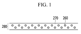
- FIG. 1 a comparative example of a light blocking member not according to but helpful to understand the present inventions is described.
- FIG. 1 is a schematic view showing a comparative example of a light blocking member not according to but helpful to understand the present invention.
- a light blocking member 280 may include a metal particle 260 and a ceramic material 270.
- the metal particle 260 and ceramic material 270 may be included in a form of a mixture or an alloy, and the mixture may include, for example the metal particle 260 dispersed in the ceramic material 270.
- the metal particle 260 may be made of an opaque metal that may include, for example silver (Ag), molybdenum (Mo), nickel (Ni), titanium (Ti), tantalum (Ta), or a combination thereof.
- the metal particle 260 may have various sizes, for example an average particle diameter of about 1 nn (10A) to about 100 nm (1,000 ⁇ ).
- the ceramic material 270 may be metal oxide that may include, for example niobium oxide, titanium oxide, aluminium oxide, or a combination thereof.
- the light blocking member 280 may reduce reflectance by scattering and/or absorbing light by the metal particle 260.
- the light blocking member 280 may have reflectance of less than or equal to about 10%, for example about 1% to about 10%.
- the light blocking member 280 may have high resistance due to the ceramic material 270 and thus may prevent parasitic capacitance from increasing between the light blocking member 280 and a metal line and/or between the light blocking member 280 and a metal electrode. Thus, deterioration of the device performance due to parasitic capacitance may be prevented.
- the light blocking member 280 may have sheet resistance ranging from about 1k ⁇ / ⁇ to 100M ⁇ / ⁇ within a thickness range of about 200 nm (2,000 ⁇ ).
- FIG. 2 is a schematic view showing a light blocking member according to an exemplary embodiment.
- the light blocking member 280 includes plural layers including a first layer 280a and a second layer 280b.
- the first layer 280a includes a metal particle 260 in a first amount and a ceramic material 270
- the second layer 280b includes the metal particle 260 in a higher second amount than the first amount and the ceramic material 270.
- the metal particle 260 is molybdenum and the ceramic material 270 is niobium oxide.
- the first amount is in the range of 1at% to 15at% based on the total amount of the metal particle 260 and the ceramic material 270
- the second amount is in the range of 10at% to 50at% based on the total amount of the metal particle 260 and the ceramic material 270.
- the first layer 280a has a higher optical transmittance, since metal particles are less disposed therein than in the second layer 280b, and accordingly, in use, is to be disposed closer to the external light incident side.
- the second layer 280b increases light scattering and absorption and thus, light blocking effects, since metal particles are more disposed in the second layer 280b than in the first layer 280a.
- the first layer 280a may partly scatter and absorb an external light, and then, the second layer 280b may mostly scatter and absorb the external light passed from the first layer 280a and thus, may decrease the external light reflection from the first layer 280a.
- the first layer 280a may have a thickness of 10 nm (100 ⁇ ) to 100 nm (1,000 ⁇ ), and the second layer 280b may have a thickness of 50 nm (500 ⁇ ) to 1000 nm (10,000 ⁇ ).
- the aforementioned light blocking member 280 may be applied to a display device.
- the display device may include, for example, a liquid crystal display (LCD), an organic light emitting diode (OLED) display, an electrophoresis display device, and the like, but the present invention is not limited thereto.
- the light blocking member 280 decreases reflection of an external light entering the display device and prevent performance deterioration of the display device, as a reflected light is recognized by a viewer. Accordingly, the light blocking member 280 does not need a separate polarizing plate on the front side of a display device to decrease the external light reflection and thus, decreases cost and simultaneously, improve light efficiency.
- a display device according to one embodiment is illustrated.
- FIG. 3 is a schematic view showing an organic light emitting diode (OLED) display according to one embodiment.
- an organic light emitting diode (OLED) display may include a switching transistor region (Qs) including a switching thin film transistor, a driving transistor region (Qd) including a driving thin film transistor, and a light emitting region (LD) including an organic light emitting diode (OLED) in each pixel.
- the switching thin film transistor has a control terminal, an input terminal, and an output terminal. The control terminal may be connected to a gate line (not shown).
- the input terminal may be connected to a data line (not shown).
- the output terminal may be connected to a driving thin film transistor.
- the switching thin film transistor responds to a scan signal applied to the gate line and transfers the data signal to the driving thin film transistor.
- the driving thin film transistor also has a control terminal, an input terminal, and an output terminal.
- the control terminal may be connected to the switching thin film transistor.
- the input terminal may be connected to a driving voltage line (not shown).
- the output terminal may be connected to an organic light emitting diode (OLED).
- OLED organic light emitting diode
- the driving thin film transistor may shed an output current with a different size depending on a voltage between the control and output terminals.
- the organic light emitting diode includes an anode connected to the output terminal of the driving thin film transistor and a cathode connected to a common voltage.
- the organic light emitting diode (OLED) emits a light depending on strength of the output current of the driving thin film transistor and displays an image.
- a light blocking member 280 may be disposed on a transparent substrate 110 that may include a glass substrate, a polymer layer, silicon wafer, or the like.
- the light blocking member 280 is formed in the display region except for the light emitting region where a pixel electrode 191, an organic light emitting member 370, and a common electrode 270 illustrated later are overlapped one another and specifically, all the display region except for the light emitting region.
- the light blocking member 280 is formed of a multi-layer each including a metal particle and a ceramic material as aforementioned with respect to the light blocking member of FIG. 2 .
- the multilayered light blocking member includes the different amount of the metal particle in the two layers.
- the first layer including the metal particle in the first amount and the ceramic material and the second layer including the metal particle in the second amount that is larger than the first amount and the ceramic material are sequentially laminated on the substrate 110.
- the metal particle is molybdenum and the ceramic material is niobium oxide.
- a switching control electrode 124a and a driving control electrode 124b are formed on the light blocking member 280.
- the switching control electrode 124a may be connected to a gate line (not shown) and receives a gate signal from the gate line.
- the driving control electrode 124b may be an island-type.
- a gate insulating layer 140 may be formed on the entire surface of the substrate 110 including the switching control electrode 124a and driving control electrode 124b.
- a switching semiconductor 154a and a driving semiconductor 154b are formed on the gate insulating layer 140.
- the switching semiconductor 154a is overlapped with the switching control electrode 124a
- the driving semiconductor 154b is overlapped with the driving control electrode 124b.
- the switching semiconductor 154a and the driving semiconductor 154b may be respectively island-types.
- a switching input electrode 173a and a switching output electrode 175a electrically connected to the switching semiconductor 154a are formed on the switching semiconductor 154a.
- the switching input electrode 173a may be connected to a data line (not shown) and receives a data signal from the data line.
- the switching output electrode 175a may be connected to a post-illustrated driving control electrode 124b.
- a driving input electrode 173b and a driving output electrode 175b electrically connected to the driving semiconductor 154b are formed on the driving semiconductor 154b.
- the driving input electrode 173b may be connected to a driving voltage line (not shown).
- the driving output electrode 175b may be connected to a post-illustrated pixel electrode 191.
- a protective layer 180 is formed on the switching input electrode 173a, the switching output electrode 175a, the driving input electrode 173b, and the driving output electrode 175b.
- the protective layer 180 has a contact hole 185 exposing the driving output electrode 175b.
- a pixel electrode 191 may be formed on the protective layer 180.
- the pixel electrode 191 may be connected to the driving output electrode 175b through the contact hole 185.
- the pixel electrode 191 may be made of, for example, conductive oxide, indium tin oxide (ITO), indium zinc oxide (IZO), aluminium doped zinc oxide (AZO), indium gallium zinc oxide (IGZO), or a combination thereof.
- a pixel definition layer 361 may be formed on the pixel electrode 191.
- the pixel definition layer 361 has an opening 365 exposing the pixel electrode 191.
- the pixel definition layer 361 surrounding the opening 365 defines a light emitting region (LD).
- the light emitting region (LD) may be formed where the pixel electrode 191 and a post-illustrated organic light emitting member 370 and common electrode 270 are overlapped one another.
- the pixel definition layer 361 may be formed of, for example, a photosensitive organic material.
- an organic light emitting member 370 may be formed.
- the organic light emitting member 370 includes an emission layer and an auxiliary layer.
- the emission layer may be made of an organic material emitting one light among primary colors such as red, green, blue, and the like or may display a white by combination of colors.
- the auxiliary layer may be positioned at least either on or under the emission layer and may include at least one selected from a hole injection layer (HIL), a hole transport layer (HTL), an electron injection layer (EIL), and an electron transport layer (ETL).
- HIL hole injection layer
- HTL hole transport layer
- EIL electron injection layer
- ETL electron transport layer
- a common electrode 270 may be formed on the pixel definition layer 361 and the organic light emitting member 370.
- the common electrode 270 may be formed of a transparent metal or a metal having a high reflectivity.
- either one of the pixel electrode 191 and the common electrode 270 is an anode, while the other is a cathode.
- the anode and the cathode as a pair flow a current to the organic light emitting member 370.
- the light blocking member 280 is formed in the display region except for the light emitting region (LD) and scatters and/or absorbs external light entering from the outside and thus, prevents the external light from being reflected by an electrode and a wire and going out again. Accordingly, the light blocking member 280 prevents visibility deterioration by an external light reflection.
- LD light emitting region
- the light blocking member 280 has high resistance and thus, may decrease parasitic capacitance with an electrode and a wire and reduce an adverse effect on operation of a device.
- FIG. 4 is a cross-sectional view showing an organic light emitting diode (OLED) display according to another embodiment.
- an organic light emitting diode (OLED) display like one according to the aforementioned embodiment, include a switching transistor region (Qs), a driving transistor region (Qd), and a light emitting region (LD) and includes a switching control electrode 124a, a driving control electrode 124b, a gate insulating layer 140, a switching semiconductor 154a, a driving semiconductor 154b, a switching input electrode 173a, a switching output electrode 175a, a driving input electrode 173b, a driving output electrode 175b, a protective layer 180, a contact hole 185, a pixel electrode 191, an organic light emitting member 370, and a common electrode 270.
- a switching transistor region Qs
- driving transistor region Qd
- LD light emitting region
- the organic light emitting diode (OLED) display unlike one according to the aforementioned embodiment, includes a light blocking member 280 formed in the display region except for the light emitting region (LD) between the thin film transistor and the common electrode 270, where the pixel electrode 191, the organic light emitting member 370, and the common electrode 270 are overlapped, rather than directly formed on a substrate 110.
- LD light emitting region
- the light blocking member 280 may simultaneously play a role of a pixel definition layer defining each pixel.
- the light blocking member 280 is formed of a multilayer each including metal particles and a ceramic material as aforementioned with respect to the light blocking member of FIG.2 .
- the multilayered light blocking member includes the different amounts of metal particles in both layers.
- the first layer including the metal particle in the first amount and the ceramic material and the second layer including the metal particle in the second amount that is larger than the first amount and the ceramic material are sequentially laminated on the protective layer 180 and the pixel electrode 191.
- the first and second layers are laminated in an opposite way. In both layers, the metal particle is molybdenum and the ceramic material is niobium oxide.
- the light blocking member 280 is formed in the display region except for the light emitting region (LD) and scattering and absorbing external light entering from the outside and thus, preventing the external light from being reflected by an electrode and a wire and going out again. Accordingly, the light blocking member 280 prevents visibility deterioration by an external light reflection.
- the light blocking member 280 has high resistance and thus, may decrease parasitic capacitance with an electrode and a wire and thus reduce an effect on operation of a device.
- FIG. 5 is a cross-sectional view showing an organic light emitting diode (OLED) display according to further embodiment.
- an organic light emitting diode (OLED) display like one according to the aforementioned embodiment, includes a switching transistor region (Qs), a driving transistor region (Qd), and a light emitting region (LD) and includes a switching control electrode 124a, a driving control electrode 124b, a gate insulating layer 140, a switching semiconductor 154a, a driving semiconductor 154b, a switching input electrode 173a, a switching output electrode 175a, a driving input electrode 173b, a driving output electrode 175b, a protective layer 180, a contact hole 185, a pixel electrode 191, an organic light emitting member 370, and a common electrode 270.
- Qs switching transistor region
- Qd driving transistor region
- LD light emitting region
- the organic light emitting diode (OLED) display unlike one according to the aforementioned embodiment, includes a light blocking member 280 formed on one surface of an encapsulation substrate 400.
- the encapsulation substrate 400 may be formed of a metal, a polymer, and the like and disposed facing the substrate 100.
- the light blocking member 280 may be formed in the display region except for the light emitting region (LD), where a pixel electrode 191, an organic light emitting member 370, and a common electrode 270 are overlapped one another, on one surface of the encapsulation substrate 400 facing the substrate 110.
- LD light emitting region
- the light blocking member 280 is formed of a multilayer each including a metal particle and a ceramic material as aforementioned with respect to the light blocking member of FIG.2 .
- the multilayered light blocking member includes the metal particle in a different amount in both layers.
- the first layer including the metal particle in the first amount and the ceramic material and the second layer including the metal particle in the second amount that is larger than the first amount and the ceramic material are sequentially laminated on the protective layer 180 and the pixel electrode 191.
- the common electrode 270 is the viewing side, the first and second layers are laminated in an opposite way.
- the light blocking member 280 is formed in the display region except for the light emitting region (LD) and scattering and absorbing external light entering from the outside and thus, preventing the light from being reflected by an electrode and a wire and going out again. Accordingly, the light blocking member 280 prevents visibility deterioration by an external light reflection. In addition, the light blocking member 280 has high resistance and thus, may decrease parasitic capacitance with an electrode and a wire and reduce an adverse effect on operation of a device.
- LD light emitting region
- Example 3 illustrates the present invention in more detail.
- Example 3 is, however, not in any sense to be interpreted as limiting the scope of this invention.
- the following Examples 1 and 2 are not according to the present invention, and, thus, are to be regarded as comparative examples, like the following Comparative Example using a single chromium layer as a light blocking member.
- Example 1 (not according to the invention):
- a mixture target of 15at% of molybdenum (Mo) particles and 85at% of a niobium oxide was prepared. Then, the mixture was sputtered on a glass substrate to form a 130 nm (1300 ⁇ )-thick light blocking member.
- a mixture target of 15at% of molybdenum (Mo) particles and 85at% of a niobium oxide was prepared. Then, the mixture was sputtered on a glass substrate to form a 150 nm (1500 ⁇ )-thick light blocking member.
- a mixture of 5at% of molybdenum (Mo) particles and 95at% of a niobium oxide was prepared. Then, the mixture was sputtered on a glass substrate to form a 500 ⁇ -thick lower light blocking member. Then, a mixture of 15at% of molybdenum (Mo) particles and 85at% of a niobium oxide was prepared. Then, the mixture was sputtered thereon to form an 800 ⁇ -thick upper light blocking member.
- Chromium (Cr) was sputtered on a glass substrate to form a 70 nm 700 ⁇ -thick light blocking member.
- the light blocking members according to Examples 1 to 3 and Comparative Example were evaluated regarding sheet resistance.
- the sheet resistance was measured in a 4-point probe method.
- the light blocking member according to Example 3 was evaluated regarding reflectance.
- the reflectance was measured using a UV-Vis spectrophotometer.
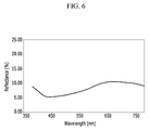
- FIG. 6 is a graph showing reflectance of the light blocking member according to Example 3.
- the light blocking member according to Example 3 had a reflectance of less than or equal to about 10% and specifically, about 5% to about 9% in a visible ray region ranging from about 400nm to about 780nm. Considering that a glass substrate itself had a reflectance of about 4%, the light blocking member according to Example 3 had a relatively low reflectance ranging from about 1 to about 5%.
Landscapes
- Physics & Mathematics (AREA)
- General Physics & Mathematics (AREA)
- Optics & Photonics (AREA)
- Engineering & Computer Science (AREA)
- Microelectronics & Electronic Packaging (AREA)
- Nonlinear Science (AREA)
- Mathematical Physics (AREA)
- Chemical & Material Sciences (AREA)
- Crystallography & Structural Chemistry (AREA)
- Electroluminescent Light Sources (AREA)
- Devices For Indicating Variable Information By Combining Individual Elements (AREA)
Description
- The present invention relates to a light blocking member and a display device including the same. A display device expresses an image and for example, includes a liquid crystal display (LCD), an organic light emitting diode (OLED) display, an electrophoretic display device, and the like.
-
US2010313875 discloses coatings comprising multilayered structures including solar absorbent layers applied to the meta surface of absorber tubes , typically stainless steel, topped with antireflective savers comprising at least two layers of refractory metal or metalloid oxides with substantially differing indices of refraction in adjacentUS2010313875 discloses for instance a double-cermet layer film structure which, from the top surface to its substrate base, consists of an anti-reflection layer that enhances solar absorption, an absorbing layer composed of two homogenous cermet layers, namely a low-metal-volume fraction cermet layer on a high-metal-volume fraction cermet layer, and a metallic infrared reflector layer to reduce substrate emittance. - The document
JP1008617 - The document
JP10341020 -
US2001010374 discloses an organic light emitting diode display device with a light shielding layer formed on the thin film transistor switching element to shield the channel region thereof. The light shielding layer may be formed of a cermet material with a metal such as Ni, Co, Fe, Cu, Cr, Ag, and Mo. - A list of conventional oxide-cermets, carbide-cermets, boride-cermets and nitride-cermets can be found in D. Hulsenberg: "Cermets", Rompp Online, Version 3.37, 31 December 2013 (URL:http://www.roempp.com/).
-
US2007069205 discloses an organic light emitting diode display device having a light shielding layer formed underneath the thin film transistor switching elements. -
US 2012056184 discloses an organic light emitting diode display device having a light shielding layer formed to cover the thin film transistor switching elements. -
US2011109596 A1 discloses an organic light emitting diode display device having an encapsulation substrate with a light shielding layer formed opposite to the non-display area. -
EP2669718 , which forms part of the state of the art pursuant to Article 54(3) EPC, discloses a light absorbing member that contains a stack of two cermet layers, each composed of metal particles dispersed in a matrix of a dielectric metal oxide ceramic, wherein the cermet layer on the viewer side of the light absorbing member has a lower concentration of metal particles, namely between 2 and 8 vol%, than the cermet layer on the far side relative to the viewer, which has a metal particle concentration between 15 and 45 vol%. The dielectric matrix is preferably formed of a niobium oxide, titanium oxide, molybdenum oxide, tungsten oxide or vanadium oxide ceramic. The metal particles are preferably formed of a noble metal like gold or silver, or a metal of the platinum group of the periodic table of the elements. -
WO2014063954 , which also forms part of the state of the art pursuant to Article 54(3) EPC, discloses a light-absorbing layer system comprising at least two layers, one layer of which is an anti-reflection layer facing the observer which is made of a dielectric material and at least one further layer of which is an absorber layer facing away from the observer made of an oxide or an oxynitride with an hypostoichiometric oxygen content. According to preferred embodiments of the light-absorbing layer system described inWO2014063954 , both layers are sputtered from a mixture target of niobium oxide (Nb2O4.99) and molybdenum, and the mixture target for sputtering the anti-reflection layer contains 10,7 wt% molybdenum and 89,3 wt% niobium oxide, while the mixture target for sputtering the absorber layer contains 36 wt% molybdenum and 64 wt% niobium oxide. - The above information disclosed in this Related Art section is only for enhancement of understanding of the background of the invention and therefore it may contain information that does not form the prior art that is already known to a person of ordinary skill in the art.
- An exemplary embodiment provides for a light blocking member as defined in appended claim 1 that prevents deterioration of display performance by an external light while reducing an effect on device performance.
- Another embodiment provides a display device that includes said light blocking member.
According an exemplary embodiment, a light blocking member as set out in claim 1 is provided. - Molybdenum and niobium oxide may be included in each layer in the form of a mixture or an alloy.
- Molybdenum and niobium oxide may be included in each layer in the form of a mixture with the molybdenum being dispersed as particles in the ceramic niobium oxide, and the molybdenum particles may then have an average particle diameter of 1 nm (10Å) to 100 nm (1,000Å).
- The first layer may have higher optical transmittance than the second layer.
- In use of the light blocking layer, the first layer is to be disposed more closely to a side exposed to external light than the second layer.
- The first layer may have a thickness of 10 nm (100Å) to 100 nm (1,000Å), and the second layer may have a thickness of 50 nm (500Å) to 1000 nm (10,000Å).
- According to another embodiment, a display device including the light blocking member of claim 1 is provided.
The display device may include a first substrate, a thin film transistor disposed on the first substrate, a first electrode electrically connected to the thin film transistor, a second electrode facing the first electrode, and a light emission layer interposed between the first electrode and the second electrode, wherein the light blocking member is disposed in planar view in a part of the display region except the light emission region where the first electrode, the second electrode, and the light emission layer are overlapped one another. - The light blocking member may be positioned in cross-sectional view between the first substrate and the thin film transistor.
- The light blocking member may be positioned in cross-sectional view between the thin film transistor and the second electrode.
The display device may further include a second substrate facing the first substrate, and the light blocking member may be positioned on one side of the second substrate.
According to a first aspect of the invention, there is a light blocking member as set out in claim 1. Preferred features are set out in claims 2 to 6.
According to a second aspect of the invention, there is a display device as set out in claim 7. Preferred features are set out in claims 8 to 11.
A more complete appreciation of the invention, and many of the attendant advantages thereof, will be readily apparent as the same becomes better understood by reference to the following detailed description when considered in conjunction with the accompanying drawings, in which like reference symbols indicate the same or similar components, wherein: -
FIG. 1 is a schematic view showing a light blocking member not according to but helpful to understand the present invention. -
FIG. 2 is a schematic view showing a light blocking member according to an embodiment. -
FIG. 3 is a schematic view showing an organic light emitting diode (OLED) display according to one embodiment. -
FIG. 4 is a cross-sectional view showing an organic light emitting diode (OLED) display according to another embodiment. -
FIG. 5 is a cross-sectional view showing an organic light emitting diode (OLED) display according to further embodiment. -
FIG. 6 is a graph showing the reflectance of the light blocking member according to Example 3. - In the drawings, the thickness of layers, films, panels, regions, etc., are exaggerated for clarity. Like reference numerals designate like elements throughout the specification. It will be understood that when an element such as a layer, film, region, or substrate is referred to as being "on" another element, it can be directly on the other element or intervening elements may also be present. In contrast, when an element is referred to as being "directly on" another element, there are no intervening elements present.
- It will be understood that when an element or layer is referred to as being, "connected to" or "coupled to" another element or layer, it can be directly connected or coupled to the other element or layer or intervening elements or layers may be present. In contrast, when an element is referred to as being "directly connected to" or "directly coupled to" another element or layer, there are no intervening elements or layers present. Like or similar reference numerals refer to like or similar elements throughout. As used herein, the term "and/or" includes any and all combinations of one or more of the associated listed items.
- It will be understood that, although the terms first, second, third etc. may be used herein to describe various elements, components, regions, layers, patterns and/or sections, these elements, components, regions, layers, patterns and/or sections should not be limited by these terms. These terms are only used to distinguish one element, component, region, layer pattern or section from another region, layer, pattern or section. Thus, a first element, component, region, layer or section discussed below could be termed a second element, component, region, layer or section without departing from the teachings of example embodiments.
- Spatially relative terms, such as "beneath," "below," "lower," "above," "upper" and the like, may be used herein for ease of description to describe one element or feature's relationship to another element(s) or feature(s) as illustrated in the figures. It will be understood that the spatially relative terms are intended to encompass different orientations of the device in use or operation in addition to the orientation depicted in the figures. For example, if the device in the figures is turned over, elements described as "below" or "beneath" other elements or features would then be oriented "above" the other elements or features. Thus, the exemplary term "below" can encompass both an orientation of above and below. The device may be otherwise oriented (rotated 90 degrees or at other orientations) and the spatially relative descriptors used herein interpreted accordingly.
- The terminology used herein is for the purpose of describing particular example embodiments only and is not intended to be limiting of the invention. As used herein, the singular forms "a," "an" and "the" are intended to include the plural forms as well, unless the context clearly indicates otherwise. It will be further understood that the terms "comprises" and/or "comprising," when used in this specification, specify the presence of stated features, integers, steps, operations, elements, and/or components, but do not preclude the presence or addition of one or more other features, integers, steps, operations, elements, components, and/or groups thereof.
Example embodiments are described herein with reference to cross sectional illustrations that are schematic illustrations of illustratively idealized example embodiments (and intermediate structures) of the inventive concept. As such, variations from the shapes of the illustrations as a result, for example, of manufacturing techniques and/or tolerances, are to be expected. Thus, example embodiments should not be construed as limited to the particular shapes of regions illustrated herein but are to include deviations in shapes that result, for example, from manufacturing. The regions illustrated in the figures are schematic in nature and their shapes are not intended to illustrate the actual shape of a region of a device and are not intended to limit the scope of the inventive concept.
Unless otherwise defined, all terms (including technical and scientific terms) used herein have the same meaning as commonly understood by one of ordinary skill in the art to which this inventive concept belongs. It will be further understood that terms, such as those defined in commonly used dictionaries, should be interpreted as having a meaning that is consistent with their meaning in the context of the relevant art and will not be interpreted in an idealized or overly formal sense unless expressly so defined herein.
In general, a display device may include a plurality of metal lines and metal electrodes. The metal lines and the metal electrodes have high reflectivity and may reflect light entering from outside. The reflected light may be recognized by a viewer and deteriorate display performance.
In order to decrease the external light reflection, a light blocking member including chromium (Cr) and absorbing an external light has been suggested. However, the light blocking member including chromium (Cr) may increase parasitic capacitance between the light blocking member and the metal lines and/or the light blocking member and the metal electrodes and thus, have an effect on device performance as well as is not environment-friendly. - Hereinafter, referring to
FIG. 1 , a comparative example of a light blocking member not according to but helpful to understand the present inventions is described. -
FIG. 1 is a schematic view showing a comparative example of a light blocking member not according to but helpful to understand the present invention. - Referring to
FIG. 1 , alight blocking member 280 may include ametal particle 260 and aceramic material 270.
Themetal particle 260 andceramic material 270 may be included in a form of a mixture or an alloy, and the mixture may include, for example themetal particle 260 dispersed in theceramic material 270. - The
metal particle 260 may be made of an opaque metal that may include, for example silver (Ag), molybdenum (Mo), nickel (Ni), titanium (Ti), tantalum (Ta), or a combination thereof. Themetal particle 260 may have various sizes, for example an average particle diameter of about 1 nn (10A) to about 100 nm (1,000Å). - The
ceramic material 270 may be metal oxide that may include, for example niobium oxide, titanium oxide, aluminium oxide, or a combination thereof.
Thelight blocking member 280 may reduce reflectance by scattering and/or absorbing light by themetal particle 260. Thelight blocking member 280 may have reflectance of less than or equal to about 10%, for example about 1% to about 10%.
In addition, thelight blocking member 280 may have high resistance due to theceramic material 270 and thus may prevent parasitic capacitance from increasing between thelight blocking member 280 and a metal line and/or between thelight blocking member 280 and a metal electrode. Thus, deterioration of the device performance due to parasitic capacitance may be prevented. Thelight blocking member 280 may have sheet resistance ranging from about 1kΩ/□ to 100MΩ/□ within a thickness range of about 200 nm (2,000Å). -
FIG. 2 is a schematic view showing a light blocking member according to an exemplary embodiment. - Referring to
FIG. 2 , thelight blocking member 280 according to an embodiment includes plural layers including afirst layer 280a and asecond layer 280b. - The
first layer 280a includes ametal particle 260 in a first amount and aceramic material 270, and thesecond layer 280b includes themetal particle 260 in a higher second amount than the first amount and theceramic material 270. In bothlayers metal particle 260 is molybdenum and theceramic material 270 is niobium oxide. The first amount is in the range of 1at% to 15at% based on the total amount of themetal particle 260 and theceramic material 270, while the second amount is in the range of 10at% to 50at% based on the total amount of themetal particle 260 and theceramic material 270. - The
first layer 280a has a higher optical transmittance, since metal particles are less disposed therein than in thesecond layer 280b, and accordingly, in use, is to be disposed closer to the external light incident side. Thesecond layer 280b increases light scattering and absorption and thus, light blocking effects, since metal particles are more disposed in thesecond layer 280b than in thefirst layer 280a. Thefirst layer 280a may partly scatter and absorb an external light, and then, thesecond layer 280b may mostly scatter and absorb the external light passed from thefirst layer 280a and thus, may decrease the external light reflection from thefirst layer 280a. - The
first layer 280a may have a thickness of 10 nm (100 Å) to 100 nm (1,000Å), and thesecond layer 280b may have a thickness of 50 nm (500 Å) to 1000 nm (10,000Å).
The aforementionedlight blocking member 280 may be applied to a display device.
The display device may include, for example, a liquid crystal display (LCD), an organic light emitting diode (OLED) display, an electrophoresis display device, and the like, but the present invention is not limited thereto. - The
light blocking member 280 decreases reflection of an external light entering the display device and prevent performance deterioration of the display device, as a reflected light is recognized by a viewer. Accordingly, thelight blocking member 280 does not need a separate polarizing plate on the front side of a display device to decrease the external light reflection and thus, decreases cost and simultaneously, improve light efficiency.
Hereinafter, a display device according to one embodiment is illustrated. - Herein, an organic light emitting diode (OLED) display as an example of the display device is illustrated referring to the following drawings.
FIG. 3 is a schematic view showing an organic light emitting diode (OLED) display according to one embodiment.
Referring toFIG. 3 an organic light emitting diode (OLED) display according to one embodiment may include a switching transistor region (Qs) including a switching thin film transistor, a driving transistor region (Qd) including a driving thin film transistor, and a light emitting region (LD) including an organic light emitting diode (OLED) in each pixel.
The switching thin film transistor has a control terminal, an input terminal, and an output terminal. The control terminal may be connected to a gate line (not shown). The input terminal may be connected to a data line (not shown). The output terminal may be connected to a driving thin film transistor. The switching thin film transistor responds to a scan signal applied to the gate line and transfers the data signal to the driving thin film transistor.
The driving thin film transistor also has a control terminal, an input terminal, and an output terminal. The control terminal may be connected to the switching thin film transistor. The input terminal may be connected to a driving voltage line (not shown). The output terminal may be connected to an organic light emitting diode (OLED). The driving thin film transistor may shed an output current with a different size depending on a voltage between the control and output terminals.
The organic light emitting diode (OLED) includes an anode connected to the output terminal of the driving thin film transistor and a cathode connected to a common voltage. The organic light emitting diode (OLED) emits a light depending on strength of the output current of the driving thin film transistor and displays an image.
Referring toFIG. 3 , alight blocking member 280 may be disposed on atransparent substrate 110 that may include a glass substrate, a polymer layer, silicon wafer, or the like. In planar view, thelight blocking member 280 is formed in the display region except for the light emitting region where apixel electrode 191, an organiclight emitting member 370, and acommon electrode 270 illustrated later are overlapped one another and specifically, all the display region except for the light emitting region. - The
light blocking member 280 is formed of a multi-layer each including a metal particle and a ceramic material as aforementioned with respect to the light blocking member ofFIG. 2 . The multilayered light blocking member includes the different amount of the metal particle in the two layers. When thesubstrate 110 is the viewing side, the first layer including the metal particle in the first amount and the ceramic material and the second layer including the metal particle in the second amount that is larger than the first amount and the ceramic material are sequentially laminated on thesubstrate 110. In both layers, the metal particle is molybdenum and the ceramic material is niobium oxide.
On thelight blocking member 280, a switchingcontrol electrode 124a and a drivingcontrol electrode 124b are formed. The switchingcontrol electrode 124a may be connected to a gate line (not shown) and receives a gate signal from the gate line. The drivingcontrol electrode 124b may be an island-type. - Then, a
gate insulating layer 140 may be formed on the entire surface of thesubstrate 110 including theswitching control electrode 124a and drivingcontrol electrode 124b.
On thegate insulating layer 140, a switchingsemiconductor 154a and a drivingsemiconductor 154b are formed. The switchingsemiconductor 154a is overlapped with the switchingcontrol electrode 124a, and the drivingsemiconductor 154b is overlapped with the drivingcontrol electrode 124b. The switchingsemiconductor 154a and the drivingsemiconductor 154b may be respectively island-types.
On the switchingsemiconductor 154a, a switchinginput electrode 173a and a switchingoutput electrode 175a electrically connected to the switchingsemiconductor 154a are formed. The switchinginput electrode 173a may be connected to a data line (not shown) and receives a data signal from the data line. The switchingoutput electrode 175a may be connected to a post-illustrateddriving control electrode 124b. - On the driving
semiconductor 154b, a drivinginput electrode 173b and a drivingoutput electrode 175b electrically connected to the drivingsemiconductor 154b are formed.
The drivinginput electrode 173b may be connected to a driving voltage line (not shown). The drivingoutput electrode 175b may be connected to apost-illustrated pixel electrode 191. - On the switching
input electrode 173a, the switchingoutput electrode 175a, the drivinginput electrode 173b, and the drivingoutput electrode 175b, aprotective layer 180 is formed. Theprotective layer 180 has acontact hole 185 exposing the drivingoutput electrode 175b. - On the
protective layer 180, apixel electrode 191 may be formed. Thepixel electrode 191 may be connected to the drivingoutput electrode 175b through thecontact hole 185. Thepixel electrode 191 may be made of, for example, conductive oxide, indium tin oxide (ITO), indium zinc oxide (IZO), aluminium doped zinc oxide (AZO), indium gallium zinc oxide (IGZO), or a combination thereof. - On the
pixel electrode 191, apixel definition layer 361 may be formed. Thepixel definition layer 361 has anopening 365 exposing thepixel electrode 191. Thepixel definition layer 361 surrounding theopening 365 defines a light emitting region (LD). The light emitting region (LD) may be formed where thepixel electrode 191 and a post-illustrated organiclight emitting member 370 andcommon electrode 270 are overlapped one another. Thepixel definition layer 361 may be formed of, for example, a photosensitive organic material. - In the light emitting region (LD) surrounded by the
pixel definition layer 361, an organiclight emitting member 370 may be formed. - The organic
light emitting member 370 includes an emission layer and an auxiliary layer. - The emission layer may be made of an organic material emitting one light among primary colors such as red, green, blue, and the like or may display a white by combination of colors.
- The auxiliary layer may be positioned at least either on or under the emission layer and may include at least one selected from a hole injection layer (HIL), a hole transport layer (HTL), an electron injection layer (EIL), and an electron transport layer (ETL).
- On the
pixel definition layer 361 and the organiclight emitting member 370, acommon electrode 270 may be formed. Thecommon electrode 270 may be formed of a transparent metal or a metal having a high reflectivity. - In the aforementioned organic light emitting device, either one of the
pixel electrode 191 and thecommon electrode 270 is an anode, while the other is a cathode. The anode and the cathode as a pair flow a current to the organiclight emitting member 370. - According to the embodiment, the
light blocking member 280 is formed in the display region except for the light emitting region (LD) and scatters and/or absorbs external light entering from the outside and thus, prevents the external light from being reflected by an electrode and a wire and going out again. Accordingly, thelight blocking member 280 prevents visibility deterioration by an external light reflection. - In addition, the
light blocking member 280 has high resistance and thus, may decrease parasitic capacitance with an electrode and a wire and reduce an adverse effect on operation of a device.
Hereinafter, referring toFIG. 4 , an organic light emitting diode (OLED) display according to another embodiment is illustrated.
FIG. 4 is a cross-sectional view showing an organic light emitting diode (OLED) display according to another embodiment. - Referring to
FIG. 4 , an organic light emitting diode (OLED) display according to the embodiment, like one according to the aforementioned embodiment, include a switching transistor region (Qs), a driving transistor region (Qd), and a light emitting region (LD) and includes aswitching control electrode 124a, a drivingcontrol electrode 124b, agate insulating layer 140, a switchingsemiconductor 154a, a drivingsemiconductor 154b, a switchinginput electrode 173a, a switchingoutput electrode 175a, a drivinginput electrode 173b, a drivingoutput electrode 175b, aprotective layer 180, acontact hole 185, apixel electrode 191, an organiclight emitting member 370, and acommon electrode 270. - However, the organic light emitting diode (OLED) display according to the embodiment, unlike one according to the aforementioned embodiment, includes a
light blocking member 280 formed in the display region except for the light emitting region (LD) between the thin film transistor and thecommon electrode 270, where thepixel electrode 191, the organiclight emitting member 370, and thecommon electrode 270 are overlapped, rather than directly formed on asubstrate 110. - The
light blocking member 280 may simultaneously play a role of a pixel definition layer defining each pixel. - The
light blocking member 280 is formed of a multilayer each including metal particles and a ceramic material as aforementioned with respect to the light blocking member ofFIG.2 . The multilayered light blocking member includes the different amounts of metal particles in both layers. - When the
substrate 110 is the viewing side, the first layer including the metal particle in the first amount and the ceramic material and the second layer including the metal particle in the second amount that is larger than the first amount and the ceramic material are sequentially laminated on theprotective layer 180 and thepixel electrode 191. Whencommon electrode 270 is the viewing side, the first and second layers are laminated in an opposite way.
In both layers, the metal particle is molybdenum and the ceramic material is niobium oxide. - According to the embodiment, the
light blocking member 280 is formed in the display region except for the light emitting region (LD) and scattering and absorbing external light entering from the outside and thus, preventing the external light from being reflected by an electrode and a wire and going out again. Accordingly, thelight blocking member 280 prevents visibility deterioration by an external light reflection.
In addition, thelight blocking member 280 has high resistance and thus, may decrease parasitic capacitance with an electrode and a wire and thus reduce an effect on operation of a device. - Hereinafter, referring to
FIG. 5 , an organic light emitting diode (OLED) display according to still another embodiment is illustrated.
FIG. 5 is a cross-sectional view showing an organic light emitting diode (OLED) display according to further embodiment.
Referring toFIG. 5 , an organic light emitting diode (OLED) display according to the embodiment, like one according to the aforementioned embodiment, includes a switching transistor region (Qs), a driving transistor region (Qd), and a light emitting region (LD) and includes aswitching control electrode 124a, a drivingcontrol electrode 124b, agate insulating layer 140, a switchingsemiconductor 154a, a drivingsemiconductor 154b, a switchinginput electrode 173a, a switchingoutput electrode 175a, a drivinginput electrode 173b, a drivingoutput electrode 175b, aprotective layer 180, acontact hole 185, apixel electrode 191, an organiclight emitting member 370, and acommon electrode 270. - However, the organic light emitting diode (OLED) display according to the embodiment, unlike one according to the aforementioned embodiment, includes a
light blocking member 280 formed on one surface of anencapsulation substrate 400. Theencapsulation substrate 400 may be formed of a metal, a polymer, and the like and disposed facing the substrate 100. Specifically, thelight blocking member 280 may be formed in the display region except for the light emitting region (LD), where apixel electrode 191, an organiclight emitting member 370, and acommon electrode 270 are overlapped one another, on one surface of theencapsulation substrate 400 facing thesubstrate 110. - The
light blocking member 280 is formed of a multilayer each including a metal particle and a ceramic material as aforementioned with respect to the light blocking member ofFIG.2 . The multilayered light blocking member includes the metal particle in a different amount in both layers. - When the
substrate 110 is a viewing side, the first layer including the metal particle in the first amount and the ceramic material and the second layer including the metal particle in the second amount that is larger than the first amount and the ceramic material are sequentially laminated on theprotective layer 180 and thepixel electrode 191. When thecommon electrode 270 is the viewing side, the first and second layers are laminated in an opposite way. - According to the embodiment, the
light blocking member 280 is formed in the display region except for the light emitting region (LD) and scattering and absorbing external light entering from the outside and thus, preventing the light from being reflected by an electrode and a wire and going out again. Accordingly, thelight blocking member 280 prevents visibility deterioration by an external light reflection.
In addition, thelight blocking member 280 has high resistance and thus, may decrease parasitic capacitance with an electrode and a wire and reduce an adverse effect on operation of a device. - The following Example 3 illustrates the present invention in more detail. Example 3 is, however, not in any sense to be interpreted as limiting the scope of this invention. The following Examples 1 and 2 are not according to the present invention, and, thus, are to be regarded as comparative examples, like the following Comparative Example using a single chromium layer as a light blocking member.
- A mixture target of 15at% of molybdenum (Mo) particles and 85at% of a niobium oxide was prepared. Then, the mixture was sputtered on a glass substrate to form a 130 nm (1300Å)-thick light blocking member.
- A mixture target of 15at% of molybdenum (Mo) particles and 85at% of a niobium oxide was prepared. Then, the mixture was sputtered on a glass substrate to form a 150 nm (1500Å)-thick light blocking member.
- A mixture of 5at% of molybdenum (Mo) particles and 95at% of a niobium oxide was prepared. Then, the mixture was sputtered on a glass substrate to form a 500Å-thick lower light blocking member. Then, a mixture of 15at% of molybdenum (Mo) particles and 85at% of a niobium oxide was prepared. Then, the mixture was sputtered thereon to form an 800Å-thick upper light blocking member.
- Chromium (Cr) was sputtered on a glass substrate to form a 70 nm 700Å-thick light blocking member.
- The light blocking members according to Examples 1 to 3 and Comparative Example were evaluated regarding sheet resistance.
- The sheet resistance was measured in a 4-point probe method.
- The results are provided in Table 1.
(Table 1) Sheet resistance (kΩ/□) Example 1 71 Example 2 67 Example 3 60 Comparative Example 4 - The light blocking member according to Example 3 was evaluated regarding reflectance.
- The reflectance was measured using a UV-Vis spectrophotometer.
- The result is provided in
FIG. 6 . -
FIG. 6 is a graph showing reflectance of the light blocking member according to Example 3. - Referring to
FIG. 6 , the light blocking member according to Example 3 had a reflectance of less than or equal to about 10% and specifically, about 5% to about 9% in a visible ray region ranging from about 400nm to about 780nm. Considering that a glass substrate itself had a reflectance of about 4%, the light blocking member according to Example 3 had a relatively low reflectance ranging from about 1 to about 5%. - While this disclosure has been described in connection with what is presently considered to be practical exemplary embodiments, it is to be understood that the invention is not limited to the disclosed embodiments, but, on the contrary, is intended to cover various modifications and equivalent arrangements included within the scope of the appended claims.
Claims (11)
- A light blocking member (280) comprising a stack of a first layer (280a) and a second layer (280b) each formed by sputtering a mixture target of a metal and a ceramic material, wherein the metal is molybdenum (260) and the ceramic material is niobium oxide (270);
wherein a first mixture target for forming the first layer (280a) includes molybdenum (260) at a first amount , and a second mixture target for forming the second layer (280b) includes molybdenum (260) at a second amount that is larger than the first amount
wherein the first amount is from 1at% to 15at% based on the total amount of molybdenum (260) and niobium oxide (270) of the first mixture target, and the second amount is from 10at% to 50at% based on
the total amount of molybdenum (260) and niobium oxide (260) of the second mixture target. - The light blocking member of claim 1, wherein molybdenum (260) and niobium oxide (270) are included in each layer (280a, 280b) in the form of a mixture or an alloy.
- The light blocking member of claim 1 or 2, wherein molybdenum (260) and niobium oxide (270) are included in each layer (280a, 280b) in the form of a mixture with the molybdenum (260) being dispersed as particles in the ceramic niobium oxide (270), and wherein the molybdenum particles (260) have an average particle diameter of 1 nm to 100 nm.
- The light blocking member of any one of claims 1 to 3, wherein the first layer (280a) has higher optical transmittance than the second layer (280b).
- The light blocking member of any one of claims 1 to 4, wherein, in use, the first layer (280a) is to be disposed more closely to a side exposed to external light than the second layer (280b).
- The light blocking member of any one of claims 1 to 5, wherein the first layer (280a) has a thickness of 10 nm to 100 nm, and the second layer (280b) has a thickness of 50 nm to 1000 nm.
- A display device, comprising:a light blocking member (280) according to any one of claims 1 to 6.
- The display device of claim 7, wherein the display device comprises:a first substrate (110);a thin film transistor disposed on the first substrate (110);a first electrode (191) electrically connected to the thin film transistor;a second electrode (270) facing the first electrode (191); anda light emission layer (370) interposed between the first electrode (191) and the second electrode (270), wherein the light blocking member (280) is disposed in planar view in the display region except the light emitting region where the first electrode (191), the second electrode (270), and the light emission layer (370) are overlapped one another.
- The display device of claim 8, wherein the light blocking member (280) is positioned in cross-sectional view between the first substrate (110) and the thin film transistor.
- The display device of claim 8, wherein the light blocking member (280) is positioned in cross-sectional view between the thin film transistor and the second electrode (270).
- The display device of any one of claims 8 to 10, wherein the display device further comprises a second substrate (400) facing the first substrate (110), and the light blocking member (280) is positioned on one side of the second substrate (400).
Applications Claiming Priority (1)
| Application Number | Priority Date | Filing Date | Title |
|---|---|---|---|
| KR1020120090234A KR101983691B1 (en) | 2012-08-17 | 2012-08-17 | Light blocking member and display panel including the same |
Publications (2)
| Publication Number | Publication Date |
|---|---|
| EP2698666A1 EP2698666A1 (en) | 2014-02-19 |
| EP2698666B1 true EP2698666B1 (en) | 2016-05-18 |
Family
ID=48782855
Family Applications (1)
| Application Number | Title | Priority Date | Filing Date |
|---|---|---|---|
| EP13172289.4A Active EP2698666B1 (en) | 2012-08-17 | 2013-06-17 | Light blocking member and display panel including the same |
Country Status (5)
| Country | Link |
|---|---|
| US (1) | US9081122B2 (en) |
| EP (1) | EP2698666B1 (en) |
| KR (1) | KR101983691B1 (en) |
| CN (1) | CN103811671B (en) |
| TW (1) | TWI613808B (en) |
Families Citing this family (15)
| Publication number | Priority date | Publication date | Assignee | Title |
|---|---|---|---|---|
| KR102055683B1 (en) * | 2013-03-29 | 2019-12-16 | 삼성디스플레이 주식회사 | Organic light emitting display apparatus |
| KR102045242B1 (en) * | 2013-06-21 | 2019-11-15 | 엘지디스플레이 주식회사 | Display apparatus |
| KR102256083B1 (en) * | 2014-03-26 | 2021-05-26 | 엘지디스플레이 주식회사 | Organic Light Emitting Display Device |
| US10061151B2 (en) * | 2014-06-30 | 2018-08-28 | Lg Display Co., Ltd. | Light shielding material and display device including the same |
| KR102230943B1 (en) * | 2014-08-14 | 2021-03-24 | 엘지디스플레이 주식회사 | Organic lighting emitting display device with light absorption and fabricating thereof |
| KR20170022047A (en) * | 2015-08-19 | 2017-03-02 | 삼성전자주식회사 | Self-luminous display panel and display apparatus having the same |
| KR102449867B1 (en) * | 2015-11-30 | 2022-09-29 | 엘지디스플레이 주식회사 | organic light emitting diode display |
| CN206441732U (en) * | 2017-02-22 | 2017-08-25 | 京东方科技集团股份有限公司 | A kind of display screen and display device |
| KR102395098B1 (en) | 2017-06-30 | 2022-05-06 | 삼성디스플레이 주식회사 | Display device and fabricating method of the same |
| CN107452758B (en) * | 2017-08-08 | 2020-05-15 | 京东方科技集团股份有限公司 | Display substrate, manufacturing method thereof and display device |
| JP2020181190A (en) * | 2019-04-24 | 2020-11-05 | 三星ディスプレイ株式會社Samsung Display Co.,Ltd. | Display device and manufacturing method therefor |
| CN110797349B (en) * | 2019-10-15 | 2022-04-05 | 深圳市华星光电半导体显示技术有限公司 | A kind of thin film transistor substrate and preparation method thereof |
| TWI732555B (en) * | 2020-02-24 | 2021-07-01 | 錼創顯示科技股份有限公司 | Micro light emitting diode structure and manufacturing method thereof and micro light emitting diode device |
| US11810904B2 (en) | 2020-02-24 | 2023-11-07 | PlayNitride Display Co., Ltd. | Micro light emitting diode structure and manufacturing method thereof and micro light emitting diode device |
| CN114664868B (en) * | 2022-03-30 | 2023-01-10 | 绵阳惠科光电科技有限公司 | Array substrate, display device and manufacturing method |
Citations (2)
| Publication number | Priority date | Publication date | Assignee | Title |
|---|---|---|---|---|
| EP2669718A1 (en) * | 2012-06-01 | 2013-12-04 | Heraeus Materials Technology GmbH & Co. KG | Light absorbing layer structure |
| WO2014063954A1 (en) * | 2012-10-23 | 2014-05-01 | Heraeus Materials Technology Gmbh & Co. Kg | Light-absorbing layer system, the production thereof and sputter target suitable therefor |
Family Cites Families (18)
| Publication number | Priority date | Publication date | Assignee | Title |
|---|---|---|---|---|
| JPH08271880A (en) * | 1995-04-03 | 1996-10-18 | Toshiba Corp | Light-shielding film, liquid crystal display device, and material for forming light-shielding film |
| CN1191614A (en) * | 1995-07-19 | 1998-08-26 | 希巴特殊化学控股公司 | Heterogeneous photo-initiators, photopolymerisable compositions and their use |
| JPH1048617A (en) | 1996-07-31 | 1998-02-20 | Toshiba Corp | Liquid crystal display device and manufacturing method thereof |
| JP3923600B2 (en) | 1997-06-09 | 2007-06-06 | 株式会社東芝 | Thin film transistor manufacturing method |
| JP4017747B2 (en) | 1998-06-04 | 2007-12-05 | 株式会社アルバック | BM film manufacturing method |
| JP2001209331A (en) | 2000-01-27 | 2001-08-03 | Tdk Corp | Thin film display |
| JP4736013B2 (en) * | 2003-12-16 | 2011-07-27 | 日本電気株式会社 | Method for manufacturing light-emitting display device |
| WO2006033304A1 (en) * | 2004-09-21 | 2006-03-30 | Sumitomo Osaka Cement Co., Ltd. | Black material, black particle dispersion liquid, black light-blocking film using same, and base with black light-blocking film |
| KR20060046935A (en) | 2004-11-12 | 2006-05-18 | 삼성코닝 주식회사 | Novel black matrix, manufacturing method thereof, and flat panel display device and electromagnetic shielding filter |
| JP2006301101A (en) * | 2005-04-18 | 2006-11-02 | Fujifilm Electronic Materials Co Ltd | Light-shielding/antireflection multilayer film, method for forming the same, solid-state imaging element having the same, and manufacturing method therefor |
| JP2007114726A (en) * | 2005-09-26 | 2007-05-10 | Sanyo Electric Co Ltd | Organic electroluminescence display device |
| US8893711B2 (en) * | 2007-10-18 | 2014-11-25 | Alliance For Sustainable Energy, Llc | High temperature solar selective coatings |
| US7666568B2 (en) * | 2007-10-23 | 2010-02-23 | E. I. Du Pont De Nemours And Company | Composition and method for providing a patterned metal layer having high conductivity |
| JP2010080328A (en) | 2008-09-26 | 2010-04-08 | Sumitomo Rubber Ind Ltd | Black colored conductive paste |
| KR101394936B1 (en) * | 2009-11-06 | 2014-05-14 | 엘지디스플레이 주식회사 | Flat plate display device with light shilding layer |
| JP2011170058A (en) | 2010-02-18 | 2011-09-01 | Canon Inc | Black matrix, manufacturing method thereof, and image display apparatus using the same |
| KR20120024241A (en) | 2010-09-06 | 2012-03-14 | 삼성모바일디스플레이주식회사 | Organic light emitting display and manufacturing method thereof |
| CN102389204A (en) * | 2011-10-27 | 2012-03-28 | 常熟市福达红木家具厂 | Rosewood dining table with lighting function |
-
2012
- 2012-08-17 KR KR1020120090234A patent/KR101983691B1/en not_active Expired - Fee Related
-
2013
- 2013-01-22 US US13/746,397 patent/US9081122B2/en active Active
- 2013-04-19 TW TW102113863A patent/TWI613808B/en active
- 2013-06-17 EP EP13172289.4A patent/EP2698666B1/en active Active
- 2013-08-16 CN CN201310369408.1A patent/CN103811671B/en active Active
Patent Citations (2)
| Publication number | Priority date | Publication date | Assignee | Title |
|---|---|---|---|---|
| EP2669718A1 (en) * | 2012-06-01 | 2013-12-04 | Heraeus Materials Technology GmbH & Co. KG | Light absorbing layer structure |
| WO2014063954A1 (en) * | 2012-10-23 | 2014-05-01 | Heraeus Materials Technology Gmbh & Co. Kg | Light-absorbing layer system, the production thereof and sputter target suitable therefor |
Also Published As
| Publication number | Publication date |
|---|---|
| KR20140023779A (en) | 2014-02-27 |
| TWI613808B (en) | 2018-02-01 |
| CN103811671A (en) | 2014-05-21 |
| US20140048829A1 (en) | 2014-02-20 |
| CN103811671B (en) | 2017-10-10 |
| US9081122B2 (en) | 2015-07-14 |
| EP2698666A1 (en) | 2014-02-19 |
| TW201409683A (en) | 2014-03-01 |
| KR101983691B1 (en) | 2019-05-30 |
Similar Documents
| Publication | Publication Date | Title |
|---|---|---|
| US9081122B2 (en) | Light blocking member and display panel including the same | |
| US12527211B2 (en) | Display apparatus and manufacturing method therefor | |
| JP5197418B2 (en) | Antireflection film, method for manufacturing the same, and display device | |
| KR102230943B1 (en) | Organic lighting emitting display device with light absorption and fabricating thereof | |
| US6897478B2 (en) | Flat panel display device with anti-reflection layer having concentration gradient | |
| EP1965233B1 (en) | Polarizer and flat panel display apparatus including the same | |
| KR102030227B1 (en) | Thin film transistor substrate and display device comprising thereof | |
| JP2003123965A (en) | Organic electroluminescent device | |
| KR19990067926A (en) | Electrode plate having transparent type or reflective type multi-layered conductive film and method for manufacturing the same | |
| EP3232262B1 (en) | Array substrate, manufacturing method therefor, and totally reflective liquid crystal display | |
| CN110968218A (en) | Touch display panel and preparation method thereof | |
| EP4478867A2 (en) | Electro-luminescence display apparatus | |
| US7538482B2 (en) | Flat display panel and black matrix thereof | |
| US20160224151A1 (en) | Electrode to be used in input device and method for producing same | |
| JP5023745B2 (en) | Transparent conductive film, transparent conductive substrate using this transparent conductive film, transparent conductive film, near-infrared shielding filter, and method for producing this transparent conductive film | |
| US20230209869A1 (en) | Display device | |
| KR101765862B1 (en) | Liquid crystal display device | |
| US20200127239A1 (en) | Display panel, method of manufacturing the same and display module having the same | |
| CN117642018A (en) | A display panel and its preparation method and display device | |
| US12507577B2 (en) | Display device | |
| EP4213000B1 (en) | Display device | |
| CN112687722A (en) | Display back plate, preparation method thereof and display panel | |
| US20250057022A1 (en) | Window and display device including the same | |
| US20250275449A1 (en) | Display device | |
| US20230273347A1 (en) | Transparent film with enhanced durability |
Legal Events
| Date | Code | Title | Description |
|---|---|---|---|
| AK | Designated contracting states |
Kind code of ref document: A1 Designated state(s): AL AT BE BG CH CY CZ DE DK EE ES FI FR GB GR HR HU IE IS IT LI LT LU LV MC MK MT NL NO PL PT RO RS SE SI SK SM TR |
|
| AX | Request for extension of the european patent |
Extension state: BA ME |
|
| PUAI | Public reference made under article 153(3) epc to a published international application that has entered the european phase |
Free format text: ORIGINAL CODE: 0009012 |
|
| 17P | Request for examination filed |
Effective date: 20140819 |
|
| RBV | Designated contracting states (corrected) |
Designated state(s): AL AT BE BG CH CY CZ DE DK EE ES FI FR GB GR HR HU IE IS IT LI LT LU LV MC MK MT NL NO PL PT RO RS SE SI SK SM TR |
|
| 17Q | First examination report despatched |
Effective date: 20150309 |
|
| RAP1 | Party data changed (applicant data changed or rights of an application transferred) |
Owner name: SAMSUNG DISPLAY CO., LTD. |
|
| GRAP | Despatch of communication of intention to grant a patent |
Free format text: ORIGINAL CODE: EPIDOSNIGR1 |
|
| RIC1 | Information provided on ipc code assigned before grant |
Ipc: G02B 5/20 20060101ALI20151027BHEP Ipc: H01L 51/52 20060101ALI20151027BHEP Ipc: H01L 27/32 20060101ALI20151027BHEP Ipc: G02F 1/1362 20060101AFI20151027BHEP |
|
| INTG | Intention to grant announced |
Effective date: 20151124 |
|
| GRAS | Grant fee paid |
Free format text: ORIGINAL CODE: EPIDOSNIGR3 |
|
| GRAA | (expected) grant |
Free format text: ORIGINAL CODE: 0009210 |
|
| AK | Designated contracting states |
Kind code of ref document: B1 Designated state(s): AL AT BE BG CH CY CZ DE DK EE ES FI FR GB GR HR HU IE IS IT LI LT LU LV MC MK MT NL NO PL PT RO RS SE SI SK SM TR |
|
| REG | Reference to a national code |
Ref country code: GB Ref legal event code: FG4D |
|
| REG | Reference to a national code |
Ref country code: CH Ref legal event code: EP |
|
| REG | Reference to a national code |
Ref country code: IE Ref legal event code: FG4D Ref country code: AT Ref legal event code: REF Ref document number: 800968 Country of ref document: AT Kind code of ref document: T Effective date: 20160615 |
|
| REG | Reference to a national code |
Ref country code: FR Ref legal event code: PLFP Year of fee payment: 4 |
|
| REG | Reference to a national code |
Ref country code: DE Ref legal event code: R096 Ref document number: 602013007548 Country of ref document: DE |
|
| REG | Reference to a national code |
Ref country code: NL Ref legal event code: FP |
|
| REG | Reference to a national code |
Ref country code: LT Ref legal event code: MG4D |
|
| PG25 | Lapsed in a contracting state [announced via postgrant information from national office to epo] |
Ref country code: FI Free format text: LAPSE BECAUSE OF FAILURE TO SUBMIT A TRANSLATION OF THE DESCRIPTION OR TO PAY THE FEE WITHIN THE PRESCRIBED TIME-LIMIT Effective date: 20160518 Ref country code: LT Free format text: LAPSE BECAUSE OF FAILURE TO SUBMIT A TRANSLATION OF THE DESCRIPTION OR TO PAY THE FEE WITHIN THE PRESCRIBED TIME-LIMIT Effective date: 20160518 Ref country code: NO Free format text: LAPSE BECAUSE OF FAILURE TO SUBMIT A TRANSLATION OF THE DESCRIPTION OR TO PAY THE FEE WITHIN THE PRESCRIBED TIME-LIMIT Effective date: 20160818 |
|
| REG | Reference to a national code |
Ref country code: AT Ref legal event code: MK05 Ref document number: 800968 Country of ref document: AT Kind code of ref document: T Effective date: 20160518 |
|
| PG25 | Lapsed in a contracting state [announced via postgrant information from national office to epo] |
Ref country code: ES Free format text: LAPSE BECAUSE OF FAILURE TO SUBMIT A TRANSLATION OF THE DESCRIPTION OR TO PAY THE FEE WITHIN THE PRESCRIBED TIME-LIMIT Effective date: 20160518 Ref country code: GR Free format text: LAPSE BECAUSE OF FAILURE TO SUBMIT A TRANSLATION OF THE DESCRIPTION OR TO PAY THE FEE WITHIN THE PRESCRIBED TIME-LIMIT Effective date: 20160819 Ref country code: RS Free format text: LAPSE BECAUSE OF FAILURE TO SUBMIT A TRANSLATION OF THE DESCRIPTION OR TO PAY THE FEE WITHIN THE PRESCRIBED TIME-LIMIT Effective date: 20160518 Ref country code: PT Free format text: LAPSE BECAUSE OF FAILURE TO SUBMIT A TRANSLATION OF THE DESCRIPTION OR TO PAY THE FEE WITHIN THE PRESCRIBED TIME-LIMIT Effective date: 20160919 Ref country code: SE Free format text: LAPSE BECAUSE OF FAILURE TO SUBMIT A TRANSLATION OF THE DESCRIPTION OR TO PAY THE FEE WITHIN THE PRESCRIBED TIME-LIMIT Effective date: 20160518 Ref country code: LV Free format text: LAPSE BECAUSE OF FAILURE TO SUBMIT A TRANSLATION OF THE DESCRIPTION OR TO PAY THE FEE WITHIN THE PRESCRIBED TIME-LIMIT Effective date: 20160518 Ref country code: HR Free format text: LAPSE BECAUSE OF FAILURE TO SUBMIT A TRANSLATION OF THE DESCRIPTION OR TO PAY THE FEE WITHIN THE PRESCRIBED TIME-LIMIT Effective date: 20160518 |
|
| PG25 | Lapsed in a contracting state [announced via postgrant information from national office to epo] |
Ref country code: IT Free format text: LAPSE BECAUSE OF FAILURE TO SUBMIT A TRANSLATION OF THE DESCRIPTION OR TO PAY THE FEE WITHIN THE PRESCRIBED TIME-LIMIT Effective date: 20160518 Ref country code: BE Free format text: LAPSE BECAUSE OF NON-PAYMENT OF DUE FEES Effective date: 20160630 |
|
| PG25 | Lapsed in a contracting state [announced via postgrant information from national office to epo] |
Ref country code: SK Free format text: LAPSE BECAUSE OF FAILURE TO SUBMIT A TRANSLATION OF THE DESCRIPTION OR TO PAY THE FEE WITHIN THE PRESCRIBED TIME-LIMIT Effective date: 20160518 Ref country code: CZ Free format text: LAPSE BECAUSE OF FAILURE TO SUBMIT A TRANSLATION OF THE DESCRIPTION OR TO PAY THE FEE WITHIN THE PRESCRIBED TIME-LIMIT Effective date: 20160518 Ref country code: RO Free format text: LAPSE BECAUSE OF FAILURE TO SUBMIT A TRANSLATION OF THE DESCRIPTION OR TO PAY THE FEE WITHIN THE PRESCRIBED TIME-LIMIT Effective date: 20160518 Ref country code: DK Free format text: LAPSE BECAUSE OF FAILURE TO SUBMIT A TRANSLATION OF THE DESCRIPTION OR TO PAY THE FEE WITHIN THE PRESCRIBED TIME-LIMIT Effective date: 20160518 Ref country code: EE Free format text: LAPSE BECAUSE OF FAILURE TO SUBMIT A TRANSLATION OF THE DESCRIPTION OR TO PAY THE FEE WITHIN THE PRESCRIBED TIME-LIMIT Effective date: 20160518 |
|
| REG | Reference to a national code |
Ref country code: CH Ref legal event code: PL |
|
| REG | Reference to a national code |
Ref country code: DE Ref legal event code: R097 Ref document number: 602013007548 Country of ref document: DE |
|
| PG25 | Lapsed in a contracting state [announced via postgrant information from national office to epo] |
Ref country code: PL Free format text: LAPSE BECAUSE OF FAILURE TO SUBMIT A TRANSLATION OF THE DESCRIPTION OR TO PAY THE FEE WITHIN THE PRESCRIBED TIME-LIMIT Effective date: 20160518 Ref country code: AT Free format text: LAPSE BECAUSE OF FAILURE TO SUBMIT A TRANSLATION OF THE DESCRIPTION OR TO PAY THE FEE WITHIN THE PRESCRIBED TIME-LIMIT Effective date: 20160518 Ref country code: SM Free format text: LAPSE BECAUSE OF FAILURE TO SUBMIT A TRANSLATION OF THE DESCRIPTION OR TO PAY THE FEE WITHIN THE PRESCRIBED TIME-LIMIT Effective date: 20160518 Ref country code: BE Free format text: LAPSE BECAUSE OF FAILURE TO SUBMIT A TRANSLATION OF THE DESCRIPTION OR TO PAY THE FEE WITHIN THE PRESCRIBED TIME-LIMIT Effective date: 20160518 |
|
| REG | Reference to a national code |
Ref country code: IE Ref legal event code: MM4A |
|
| PLBE | No opposition filed within time limit |
Free format text: ORIGINAL CODE: 0009261 |
|
| STAA | Information on the status of an ep patent application or granted ep patent |
Free format text: STATUS: NO OPPOSITION FILED WITHIN TIME LIMIT |
|
| PG25 | Lapsed in a contracting state [announced via postgrant information from national office to epo] |
Ref country code: MC Free format text: LAPSE BECAUSE OF FAILURE TO SUBMIT A TRANSLATION OF THE DESCRIPTION OR TO PAY THE FEE WITHIN THE PRESCRIBED TIME-LIMIT Effective date: 20160518 |
|
| 26N | No opposition filed |
Effective date: 20170221 |
|
| PG25 | Lapsed in a contracting state [announced via postgrant information from national office to epo] |
Ref country code: LI Free format text: LAPSE BECAUSE OF NON-PAYMENT OF DUE FEES Effective date: 20160630 Ref country code: CH Free format text: LAPSE BECAUSE OF NON-PAYMENT OF DUE FEES Effective date: 20160630 |
|
| PG25 | Lapsed in a contracting state [announced via postgrant information from national office to epo] |
Ref country code: SI Free format text: LAPSE BECAUSE OF FAILURE TO SUBMIT A TRANSLATION OF THE DESCRIPTION OR TO PAY THE FEE WITHIN THE PRESCRIBED TIME-LIMIT Effective date: 20160518 Ref country code: IE Free format text: LAPSE BECAUSE OF NON-PAYMENT OF DUE FEES Effective date: 20160617 |
|
| REG | Reference to a national code |
Ref country code: FR Ref legal event code: PLFP Year of fee payment: 5 |
|
| REG | Reference to a national code |
Ref country code: FR Ref legal event code: PLFP Year of fee payment: 6 |
|
| PG25 | Lapsed in a contracting state [announced via postgrant information from national office to epo] |
Ref country code: HU Free format text: LAPSE BECAUSE OF FAILURE TO SUBMIT A TRANSLATION OF THE DESCRIPTION OR TO PAY THE FEE WITHIN THE PRESCRIBED TIME-LIMIT; INVALID AB INITIO Effective date: 20130617 Ref country code: CY Free format text: LAPSE BECAUSE OF FAILURE TO SUBMIT A TRANSLATION OF THE DESCRIPTION OR TO PAY THE FEE WITHIN THE PRESCRIBED TIME-LIMIT Effective date: 20160518 |
|
| PG25 | Lapsed in a contracting state [announced via postgrant information from national office to epo] |
Ref country code: LU Free format text: LAPSE BECAUSE OF NON-PAYMENT OF DUE FEES Effective date: 20160617 Ref country code: MT Free format text: LAPSE BECAUSE OF NON-PAYMENT OF DUE FEES Effective date: 20160630 Ref country code: IS Free format text: LAPSE BECAUSE OF FAILURE TO SUBMIT A TRANSLATION OF THE DESCRIPTION OR TO PAY THE FEE WITHIN THE PRESCRIBED TIME-LIMIT Effective date: 20160518 Ref country code: TR Free format text: LAPSE BECAUSE OF FAILURE TO SUBMIT A TRANSLATION OF THE DESCRIPTION OR TO PAY THE FEE WITHIN THE PRESCRIBED TIME-LIMIT Effective date: 20160518 Ref country code: MK Free format text: LAPSE BECAUSE OF FAILURE TO SUBMIT A TRANSLATION OF THE DESCRIPTION OR TO PAY THE FEE WITHIN THE PRESCRIBED TIME-LIMIT Effective date: 20160518 |
|
| PG25 | Lapsed in a contracting state [announced via postgrant information from national office to epo] |
Ref country code: BG Free format text: LAPSE BECAUSE OF FAILURE TO SUBMIT A TRANSLATION OF THE DESCRIPTION OR TO PAY THE FEE WITHIN THE PRESCRIBED TIME-LIMIT Effective date: 20160518 |
|
| PG25 | Lapsed in a contracting state [announced via postgrant information from national office to epo] |
Ref country code: AL Free format text: LAPSE BECAUSE OF FAILURE TO SUBMIT A TRANSLATION OF THE DESCRIPTION OR TO PAY THE FEE WITHIN THE PRESCRIBED TIME-LIMIT Effective date: 20160518 |
|
| P01 | Opt-out of the competence of the unified patent court (upc) registered |
Effective date: 20230515 |
|
| PGFP | Annual fee paid to national office [announced via postgrant information from national office to epo] |
Ref country code: NL Payment date: 20250520 Year of fee payment: 13 |
|
| PGFP | Annual fee paid to national office [announced via postgrant information from national office to epo] |
Ref country code: DE Payment date: 20250520 Year of fee payment: 13 |
|
| PGFP | Annual fee paid to national office [announced via postgrant information from national office to epo] |
Ref country code: GB Payment date: 20250520 Year of fee payment: 13 |
|
| PGFP | Annual fee paid to national office [announced via postgrant information from national office to epo] |
Ref country code: FR Payment date: 20250521 Year of fee payment: 13 |