EP2697627B1 - Fluorescence imaging system and method - Google Patents
Fluorescence imaging system and method Download PDFInfo
- Publication number
- EP2697627B1 EP2697627B1 EP12771262.8A EP12771262A EP2697627B1 EP 2697627 B1 EP2697627 B1 EP 2697627B1 EP 12771262 A EP12771262 A EP 12771262A EP 2697627 B1 EP2697627 B1 EP 2697627B1
- Authority
- EP
- European Patent Office
- Prior art keywords
- sensor
- sample platform
- light
- illumination
- targeted area
- Prior art date
- Legal status (The legal status is an assumption and is not a legal conclusion. Google has not performed a legal analysis and makes no representation as to the accuracy of the status listed.)
- Active
Links
Images



Classifications
-
- G—PHYSICS
- G01—MEASURING; TESTING
- G01N—INVESTIGATING OR ANALYSING MATERIALS BY DETERMINING THEIR CHEMICAL OR PHYSICAL PROPERTIES
- G01N21/00—Investigating or analysing materials by the use of optical means, i.e. using sub-millimetre waves, infrared, visible or ultraviolet light
- G01N21/62—Systems in which the material investigated is excited whereby it emits light or causes a change in wavelength of the incident light
- G01N21/63—Systems in which the material investigated is excited whereby it emits light or causes a change in wavelength of the incident light optically excited
- G01N21/64—Fluorescence; Phosphorescence
- G01N21/645—Specially adapted constructive features of fluorimeters
- G01N21/6456—Spatial resolved fluorescence measurements; Imaging
-
- G—PHYSICS
- G02—OPTICS
- G02B—OPTICAL ELEMENTS, SYSTEMS OR APPARATUS
- G02B21/00—Microscopes
- G02B21/16—Microscopes adapted for ultraviolet illumination ; Fluorescence microscopes
-
- G—PHYSICS
- G01—MEASURING; TESTING
- G01N—INVESTIGATING OR ANALYSING MATERIALS BY DETERMINING THEIR CHEMICAL OR PHYSICAL PROPERTIES
- G01N21/00—Investigating or analysing materials by the use of optical means, i.e. using sub-millimetre waves, infrared, visible or ultraviolet light
- G01N21/17—Systems in which incident light is modified in accordance with the properties of the material investigated
- G01N2021/178—Methods for obtaining spatial resolution of the property being measured
- G01N2021/1785—Three dimensional
Definitions
- the present invention relates to optical imaging with reduced background, and more specifically to systems and methods for directly measuring the amount of background noise and removing it from the detected signal.
- Fluorescence imaging is one of the techniques that have significant capabilities to reliably achieve sensitive, quantitative measurements.
- the target to be imaged is illuminated by an optical signal having a first spectral content (excitation light), and a portion of such a signal is absorbed by at least part of the target and is re-emitted as an optical signal of a second spectral content (emission light).
- the emission light is then detected by a detection system as a measure of the properties of the target.
- a fluorescence imaging system typically includes one or more sources and components that generate and deliver the excitation light to the target area.
- the system also includes components to collect light from the target area, separate the emission light from the excitation light, and deliver it to an optical sensor.
- One common method for separating the emission light from reflected and/or scattered excitation light is optical filtering.
- Various other methods are also used to achieve similar results.
- it is often difficult to completely prevent reflected and/or scattered excitation light from reaching the sensor. This adds an amount of non-fluorescence signal to the emission signal which, in turn, results in a non-accurate measurement of target properties such as quantity of fluorescence material. This is one type of optical background noise.
- optical background Another known type of optical background is auto-fluorescence which results from non-target elements in the system absorbing a portion of the excitation light and re-emitting it as fluorescence, a portion of its content being within the second spectral range.
- components that can generate auto-fluorescence background noise include the media where the target resides, optical filters, and lenses. Yet another source of optical background noise towards the sensor.
- non-optical background sources such as dark signals generated by the sensor itself and the electronics that drive it. They, too, cause an increase in the background noise and if not eliminated or reduced, limit the performance of the imaging system.
- US 2007/0064990 A1 discloses a fluorescence imaging system comprising the features recited in the preamble of claim 1.
- the present invention provides systems and methods for reducing or eliminating background-related noise in optical imaging signals, and particularly fluorescence imaging signals.
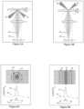
- FIG. 1A One type of fluorescence scanning system configuration is depicted by Figure 1A .
- a platform 1 such as a glass plate, membrane coated slide, or other transparent, semi-transparent, and/or opaque media.
- a target area on the platform is illuminated by excitation light 4 which can be generated from laser source(s), LEDs, or broadband lamps and collected with some optical elements.
- the illumination light is typically filtered out using optical filters, dispersive elements, and the like to restrict the spectral content that arrives at the target plane, for example to excite only one of more than one fluorescence labels in the target plane.
- the fluorescence labels absorb a portion of the excitation light and the fluorescence emission is then collected through part of the detection system 2a and focused by another part of the detection system 2b onto a detector or sensor 3.
- One key aspect of this scanning method is that the excitation light and the collected emission light share part of the optical system, i.e. they are coaxial at the target plane.
- the paths are combined using, typically, a dichroic filter element 5 that reflects excitation light 4 towards the target 1 and transmits the emission light 5a towards the sensor 3.
- Another useful set-up includes a dichroic element 5 that transmits excitation light 4 towards the target 1 and reflects emission light 5a towards the sensor 3.
- Dichroic element 5 is typically mounted at an angle, for example 45°, in order to allow for mounting the source optics and sensor optics independently.
- Figure 1A Other components necessary for detecting fluorescence are not included in Figure 1A , but should be obvious to skilled in the art to recognize them and ways they can be included.
- One of such elements is emission filters. These are typically needed to block most of the excitation light that reflects off of the target area and allows emission light to reach the sensor. These can include more than one type of filter. For example, a notch filter to block most of the emission light and a band-pass filter to further block any residual excitation light leaking through the notch filter and further distinguish the desired emission light from other non-desired light.
- US Patent No. 7,286,232 which is incorporated by reference in its entirety, discusses various aspects of useful imaging optics. So, Figure 1A is to be interpreted as an indication of the coaxial nature of excitation and emission light paths and point out some of the sources of background noise addressed herein.
- the illumination pattern in the target area is a point, a number of points, a line, or number of lines and the sample platform and/or the optical system are scanned in one or both directions to build up an image of larger area.
- scanning can be achieved by moving the illumination light across the target area while the detection system and the target sample remain fixed. This can be done by a scanning mirror, for example, that sequentially aims the illumination beam at different locations over time and the detection system is accordingly aimed at those locations.
- scanning can be achieved by moving the sample platform relative to a fixed illumination and detection system, or by moving both the illumination and detection systems while holding the sample platform fixed.
- Figure 1B is another example of coaxial illumination system, but in transmission mode instead of reflection mode as shown in FIG. 1A .
- This is also a common mode of imaging and can have various types of illumination patterns and additional elements as in the case of Figure 1A .
- the target area of the platform transparent or semi-transparent
- Light 4 can be generated from laser source(s), LEDs, or broadband lamps.
- a combining dichroic element is typically not needed and element 5 shown in Figure 1B refers to a blocking filter function, such as by a notch filter, that blocks most of the illumination light that passes through the target area.
- the blocking element 5 can be mounted at any angle, for example 8°, sufficient for its reflection to end up far enough from the field of view of the sensor and thus avoid any significant ghost reflections.
- FIGS. 1A and 1B show two areas where optical background noise is typically generated and reaches the sensor. These are labeled as 5b and 5c.
- the former can be a result of part of the excitation light that bounces around in the vicinity of the target area and ends up generating some fluorescence light from the mounting media (auto-fluorescence) and any non-specific binding. This is more significant for membrane mounted targets where the membrane generates some auto-fluorescence and diffuses light around to cover an area wider than the desired target size.
- mounting media such as membranes diffuse part of the fluorescence light emitted from the target area itself in a similar manner. This results in some optical signal reaching the sensor and typically covers a wide area that includes the target image. Because of its diffusion and the variations in its origins, optical background 5b usually results in a relatively small, non-localized, background signal detected by the sensor.
- optical background can be generated in the optical elements such as in dichroic elements or blocking filters 5.
- This is mainly a result of the relatively high power of illumination light used, which causes auto-fluorescence emission 5c in the materials of such filters and optical elements in its path.
- Signal 5c can also include portions of illumination light that scatters off impurity particles or dust particles and end up leaking through to the sensor. In a manner similar to background light 5b, this also results in weak signal broadly distributed over the sensor area.
- Yet another source of optical background can be a leakage from ambient light or from other light sources within the system.
- any leakage is most likely to be predominantly non-localized and covers a large area of the sensor that includes the image of the target.
- Figures 2A and 2B show typical patterns that target emission light 5a and background light 5b and 5c make at the sensor area for the cases of point-scanning and line-scanning, respectively.
- the fluorescence originating from the target area 5a when in focus, is typically focused to a localized area that forms the image of the target.
- background light 5b and 5c and any other light leakage reach the sensor spread over a wider area that includes the area where signal 5a reaches but also includes another portion of the sensor where there is little light from signal 5a.
- this difference between desired fluorescence light 5a and un-desired background light (5b + 5c) is leveraged.
- the actual signal S can easily be obtained by subtracting S 2 from S 1 .
- This subtraction can be accomplished directly through readout circuitry or in post measurement calculations. The latter can be accomplished with minimal additions of noise by applying a low-pass filter onto S 2 to eliminate the high frequency shot noise typically present with most detectors and thus the subtraction step does not add any to the measurement of S 1 , i.e., the resultant noise in S is comparable to the noise present in S 1 , which is the desired outcome.
- An array sensor such as a CCD sensor or a CMOS sensor ( Figures 2A and 2B ).
- An array sensor can be configured so that one or more of its elements 3a read S 1 and one or more of its other elements 3b read S 2 .
- the subtraction can be easily performed post detection and for CMOS, it can also be performed through the readout circuitry.
- FIG. 3A and 3B Another type of fluorescence scanning is depicted in Figures 3A and 3B .
- detection can be in reflection mode ( Figure 3A ) or in transmission mode ( Figure 3B ) and the illumination pattern can be in the form of one or more spots or lines.
- This method differs from those depicted by Figures 1A and 1B , and described above, in that the illumination 4a impinges onto the target area at an angle, either from the front side (reflection mode) or the backside (transmission mode).
- Typical angles of incidences can range from a few degrees to more than 45°. The selection of the optimum angle is a trade-off between available working distances and positional sensitivities along the optical axis.
- Figures 4A and 4B like Figures 2A and 2B , show typical patterns that target emission light 5a and background light 5b make at the sensor area for the common cases of point-scanning and line-scanning, respectively.
- Angling the illumination offers the advantage of reflecting any of the specular reflections away from the detection collection optics and thus produces a much reduced optical signal to block by filters which, in turn, results in reduced background levels registered by the sensor. Another advantage is that excitation light does not pass through components in the emission path and thus there are less chances of generating auto-fluorescence 5c.
- the main contributor to the optical background signal in this case is from the target mounting medium, i.e. signal 5b.
- Applying the differential measurement method described above can eliminate or reduce this background significantly.
- FIG. 5 Another embodiment of the invention follows the angular illumination method of Figure 3A and is shown in Figure 5 where laser line scanning and array detection, e.g., CCD array detection, are used.
- An excitation laser beam 4a is incident on a target surface 1b at an angle of incidence such that most of the specular reflections 4b miss the fluorescence collecting optics 2.
- the laser light is preferably shaped to focus on a line perpendicular to the plane of incidence. It is preferable that such illuminating line be substantially uniform along its length and narrow in the other direction, for example diffraction-limited.
- the laser line excites fluorescently-labeled target areas which are then imaged onto a CCD array or other array.
- Such a detector array should be chosen with low dark current and read-noise so that any dark background is minimal.
- S 1 and S 2 can be obtained by binning 10 rows each, i.e. rows 3a and 3b, respectively.
- the differential measure of the amount of fluorescence present is then obtained by subtracting S 2 from S 1 .
- a target area is imaged by scanning the target sample 1 and/or the optical system in one or both directions.
- two line images are obtained: One image by binning one or more rows around the image of the laser line location and another image by binning one or more rows away from the image of laser line location. These are designated in Figure 5 as S 1 and S 2 , respectively.
- an opaque mask can be used as shown to facilitate image collection with reduced background.
- ICX285AL sensor chip An example of a useful low-noise CCD is the Sony ICX285AL sensor chip.
- This chip is an interline type, where photo-generated charges are transferred row by row towards the output register which is then read-out serially.
- One or more rows can be added together (binned) at the output register before they're read out and the result is a row of signals that can represent the image of one line.
- the ICX285AL is capable of binning rows together with minimal additional noise when cooled. Cooling requirements are set by the maximum number of rows to bin and the longest exposure time per each line image. For example, 0°C cooling with the ICX285AL produces minimal dark current for exposures less than 50ms and binning up to 20 rows each.
- sensors and arrays of sensors can be used to accomplish the differential read described above.
- one or more of the same or different sensors may be used, e.g., a single CCD or an array of CCDs or a single CMOS or an array of CMOS sensors.
- Other useful sensors might include photodiodes, avalanche photodiodes (APDs), silicon photomultiplier devices, an array of photomultiplier tubes, a focal plane array, etc.
- the result of a scan is two images: One image of the fluorescence target area that includes any background present, S 1 , and another image that consists primarily of background, S 2 .
- the latter is preferably filtered with a low-pass filter to reduce its read-noise and then subtracted from the former.
- lpfilter() is a low-pass filter function applied to the background image S 2 .
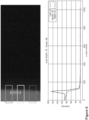
- Figure 6 shows one example of the CCD frames obtained at one scan position according to one embodiment. The sample is positioned so that the laser line illumination crosses a fluorescently labeled spot about 2mm in diameter.
- the display of the image is enhanced to show the residual background signal in the neighborhood of the line cross-section of the spot and clearly indicates that the background signal extends beyond the image of the line and is relatively constant across a number of rows.
- Figure 6 also shows a three-plot cross-sections indicated by the top (left), center (middle), and bottom (right) rectangles on the image.
- the x-axis for the plots is CCD row numbers and the y-axis is signal level.
- the plots give an indication of the level of background signal and spot fluorescence.
- Figure 7 shows the two scans obtained with the differential scanner S 1 and S 2 along with the calculated differential scan S. Also shown in Figure 7 are 3 cross-section plots at the dashed lines across the three images. They show the level of background signal in each of scans S 1 and S 2 and the resulting minimum background level in the resulting differential scan.
- Imaging by differential scanning advantageously relaxes the requirements for enclosure light tightness. Any residual optical background resulting from ambient lighting is automatically reduced or removed and the result is a background-free or background-reduced image. Also, differential scanning produces effects similar to confocal imaging. Light originating from out of focus areas produce spatially broad patterns at the sensor, i.e., relatively constant over the areas where both S 1 and S 2 are measured. This means that a differential scanning measurement will remove most of the out of focus background and produces "confocal-like" images.
- scanning can include a third dimension (x, y and z) to obtain background-reduced two-dimensional images (x, y) at different depths (z). These images obtained at different depths can be combined to produce background-reduced, confocal-like, three-dimensional images (e.g., a volume).
- the targeted area is scanned over the sample platform so as to build up a two dimensional image of a sample on the sample platform at a first depth of focus, and then, one or more times, the depth of focus is adjusted and the targeted area is scanned over the sample platform so as to build up a two dimensional image of a sample on the sample platform at a different depth of focus.
- a scanning mechanism includes a mechanism to adjust the depth of focus (perpendicular to plane of sample platform).
Landscapes
- Physics & Mathematics (AREA)
- Health & Medical Sciences (AREA)
- Analytical Chemistry (AREA)
- General Physics & Mathematics (AREA)
- Chemical & Material Sciences (AREA)
- Nuclear Medicine, Radiotherapy & Molecular Imaging (AREA)
- Optics & Photonics (AREA)
- Life Sciences & Earth Sciences (AREA)
- Biochemistry (AREA)
- General Health & Medical Sciences (AREA)
- Immunology (AREA)
- Pathology (AREA)
- Investigating, Analyzing Materials By Fluorescence Or Luminescence (AREA)
Description
- The present invention relates to optical imaging with reduced background, and more specifically to systems and methods for directly measuring the amount of background noise and removing it from the detected signal.
- Optical imaging is becoming more and more the method of choice for many measurement applications that demand high sensitivity and quantification. Recent scientific advances benefit from reliably detecting small and/or weak targets. In order to obtain reliable representations of such targets, it is desirable to use an imaging system that has low noise levels. Fluorescence imaging is one of the techniques that have significant capabilities to reliably achieve sensitive, quantitative measurements. With fluorescence imaging, the target to be imaged is illuminated by an optical signal having a first spectral content (excitation light), and a portion of such a signal is absorbed by at least part of the target and is re-emitted as an optical signal of a second spectral content (emission light). The emission light is then detected by a detection system as a measure of the properties of the target.
- A fluorescence imaging system typically includes one or more sources and components that generate and deliver the excitation light to the target area. The system also includes components to collect light from the target area, separate the emission light from the excitation light, and deliver it to an optical sensor. One common method for separating the emission light from reflected and/or scattered excitation light is optical filtering. Various other methods are also used to achieve similar results. However, with all the techniques known to date, it is often difficult to completely prevent reflected and/or scattered excitation light from reaching the sensor. This adds an amount of non-fluorescence signal to the emission signal which, in turn, results in a non-accurate measurement of target properties such as quantity of fluorescence material. This is one type of optical background noise. Another known type of optical background is auto-fluorescence which results from non-target elements in the system absorbing a portion of the excitation light and re-emitting it as fluorescence, a portion of its content being within the second spectral range. Examples of components that can generate auto-fluorescence background noise include the media where the target resides, optical filters, and lenses. Yet another source of optical background noise towards the sensor. There are also a number of other non-optical background sources, such as dark signals generated by the sensor itself and the electronics that drive it. They, too, cause an increase in the background noise and if not eliminated or reduced, limit the performance of the imaging system.
- There are a number of techniques and implementations for improving the sensitivity of fluorescence imaging systems (see, e.g.,
US Patent No. 6,921,908 ;US Patent No. 6,495,812 ;US Patent No. 7,286,232 ; andUS Patent Application No. 12/785,308 ). These techniques range from hardware configurations to software processing of acquired images. For example, software processing solutions include that disclosed inWO 2010/084381 which provides a method whereby the local background noise value is subtracted from the detected signal. Methods that rely more on hardware techniques are often preferred because they aim at the root-cause of the problems not at their symptoms. Within the hardware solutions, the most efficient are those that leverage any differences between the optical properties of target fluorescence emission and background noise to favorably select the former. And, as is well known in the optical imaging industry, techniques that work best for one type of background noise may not work well for others. There are also techniques that address more than one type of background noise in one design, but there still is a need for a more general way to eliminate or reduce the background noise irrespective of its origin or type. - Therefore it is desirable to provide systems and methods that overcome the above and other problems.
US 2007/0064990 A1 discloses a fluorescence imaging system comprising the features recited in the preamble ofclaim 1. - The present invention is set forth in the appended claims.
-
-
FIGS. 1A-B illustrate a fluorescence scanning system configuration according to one embodiment using coaxial illumination;FIG. 1A illustrates the system in reflection mode andFIG. 1B illustrates the system in transmission mode. -
FIGS. 2A and 2B show typical patterns that target emission light and background light make at the sensor area for the cases of point-scanning and line-scanning, respectively, of the configurations shown inFIG. 1 . -
FIGS. 3A-B illustrate a fluorescence scanning system configuration according to one embodiment using angled illumination;FIG. 3A illustrates the system in reflection mode andFIG. 3B illustrates the system in transmission mode. -
FIGS. 4A and 4B show typical patterns that target emission light and background light make at the sensor area for the cases of point-scanning and line-scanning, respectively, of the configurations shown inFIGS. 3A and 3B . -
FIG. 5 illustrates laser line scanning and array detection with angular illumination (in reflection mode) according to one embodiment. -
FIG. 6 shows one example of the CCD frames obtained at one scan position for the embodiment shown inFIG. 5 , and three-plot cross-sections indicated by the top (left), center (middle), and bottom (right) rectangles on the image. -
FIG. 7 shows the two scans obtained with the differential scanner S1 and S2 along with the calculated differential scan S. Also shown inFigure 7 are 3 cross-section plots at the dashed lines across the three images. - The present invention provides systems and methods for reducing or eliminating background-related noise in optical imaging signals, and particularly fluorescence imaging signals.
- One type of fluorescence scanning system configuration is depicted by
Figure 1A . One or more fluorescently labeled targets are mounted on aplatform 1 such as a glass plate, membrane coated slide, or other transparent, semi-transparent, and/or opaque media. A target area on the platform is illuminated by excitation light 4 which can be generated from laser source(s), LEDs, or broadband lamps and collected with some optical elements. The illumination light is typically filtered out using optical filters, dispersive elements, and the like to restrict the spectral content that arrives at the target plane, for example to excite only one of more than one fluorescence labels in the target plane. The fluorescence labels absorb a portion of the excitation light and the fluorescence emission is then collected through part of the detection system 2a and focused by another part of the detection system 2b onto a detector orsensor 3. One key aspect of this scanning method is that the excitation light and the collected emission light share part of the optical system, i.e. they are coaxial at the target plane. The paths are combined using, typically, a dichroic filter element 5 that reflects excitation light 4 towards thetarget 1 and transmits the emission light 5a towards thesensor 3. Another useful set-up includes a dichroic element 5 that transmits excitation light 4 towards thetarget 1 and reflects emission light 5a towards thesensor 3. Dichroic element 5 is typically mounted at an angle, for example 45°, in order to allow for mounting the source optics and sensor optics independently. - Other components necessary for detecting fluorescence are not included in
Figure 1A , but should be obvious to skilled in the art to recognize them and ways they can be included. One of such elements is emission filters. These are typically needed to block most of the excitation light that reflects off of the target area and allows emission light to reach the sensor. These can include more than one type of filter. For example, a notch filter to block most of the emission light and a band-pass filter to further block any residual excitation light leaking through the notch filter and further distinguish the desired emission light from other non-desired light.US Patent No. 7,286,232 , which is incorporated by reference in its entirety, discusses various aspects of useful imaging optics. So,Figure 1A is to be interpreted as an indication of the coaxial nature of excitation and emission light paths and point out some of the sources of background noise addressed herein. - In accordance with the invention, the illumination pattern in the target area is a point, a number of points, a line, or number of lines and the sample platform and/or the optical system are scanned in one or both directions to build up an image of larger area. For example, scanning can be achieved by moving the illumination light across the target area while the detection system and the target sample remain fixed. This can be done by a scanning mirror, for example, that sequentially aims the illumination beam at different locations over time and the detection system is accordingly aimed at those locations. As another example, scanning can be achieved by moving the sample platform relative to a fixed illumination and detection system, or by moving both the illumination and detection systems while holding the sample platform fixed.
-
Figure 1B is another example of coaxial illumination system, but in transmission mode instead of reflection mode as shown inFIG. 1A . This is also a common mode of imaging and can have various types of illumination patterns and additional elements as in the case ofFigure 1A . In this transmission mode, the target area of the platform (transparent or semi-transparent) is illuminated by excitation light 4, which impinges on theplatform 1 from the backside of the platform relative to the optical detection system. Light 4 can be generated from laser source(s), LEDs, or broadband lamps. A combining dichroic element is typically not needed and element 5 shown inFigure 1B refers to a blocking filter function, such as by a notch filter, that blocks most of the illumination light that passes through the target area. The blocking element 5 can be mounted at any angle, for example 8°, sufficient for its reflection to end up far enough from the field of view of the sensor and thus avoid any significant ghost reflections. - Both
Figures 1A and 1B show two areas where optical background noise is typically generated and reaches the sensor. These are labeled as 5b and 5c. The former can be a result of part of the excitation light that bounces around in the vicinity of the target area and ends up generating some fluorescence light from the mounting media (auto-fluorescence) and any non-specific binding. This is more significant for membrane mounted targets where the membrane generates some auto-fluorescence and diffuses light around to cover an area wider than the desired target size. In addition, mounting media such as membranes diffuse part of the fluorescence light emitted from the target area itself in a similar manner. This results in some optical signal reaching the sensor and typically covers a wide area that includes the target image. Because of its diffusion and the variations in its origins, optical background 5b usually results in a relatively small, non-localized, background signal detected by the sensor. - Another area where optical background can be generated is in the optical elements such as in dichroic elements or blocking filters 5. This is mainly a result of the relatively high power of illumination light used, which causes auto-fluorescence emission 5c in the materials of such filters and optical elements in its path. Signal 5c can also include portions of illumination light that scatters off impurity particles or dust particles and end up leaking through to the sensor. In a manner similar to background light 5b, this also results in weak signal broadly distributed over the sensor area. Yet another source of optical background can be a leakage from ambient light or from other light sources within the system. Here, too, because of their locations relative to the sensor, any leakage is most likely to be predominantly non-localized and covers a large area of the sensor that includes the image of the target.
-
Figures 2A and 2B show typical patterns that target emission light 5a and background light 5b and 5c make at the sensor area for the cases of point-scanning and line-scanning, respectively. The fluorescence originating from the target area 5a, when in focus, is typically focused to a localized area that forms the image of the target. However, background light 5b and 5c and any other light leakage reach the sensor spread over a wider area that includes the area where signal 5a reaches but also includes another portion of the sensor where there is little light from signal 5a. In certain aspects this difference between desired fluorescence light 5a and un-desired background light (5b + 5c) is leveraged. If the portion of the sensor area where most of 5a and a portion of (5b + 5c) reach and another portion of the sensor area where a minimum amount of 5a reaches but a similar amount of (5b + 5c) reaches are detected separately, the following two readings are obtained:

- If the sensor areas are selected so that the second reading S 2 is comparable to the 'B' component of S1, then the actual signal S can easily be obtained by subtracting S 2 from S 1. This subtraction can be accomplished directly through readout circuitry or in post measurement calculations. The latter can be accomplished with minimal additions of noise by applying a low-pass filter onto S2 to eliminate the high frequency shot noise typically present with most detectors and thus the subtraction step does not add any to the measurement of S 1, i.e., the resultant noise in S is comparable to the noise present in S 1, which is the desired outcome.
- Various types of sensor configurations can be used to accomplish this "Signal - Background" difference measurement. One typical type of sensors that lends itself easily to such an operation is an array sensor such as a CCD sensor or a CMOS sensor (
Figures 2A and 2B ). An array sensor can be configured so that one or more of itselements 3a read S1 and one or more of itsother elements 3b read S 2. For CCDs, the subtraction can be easily performed post detection and for CMOS, it can also be performed through the readout circuitry. - Another type of fluorescence scanning is depicted in
Figures 3A and 3B . Here, too, detection can be in reflection mode (Figure 3A ) or in transmission mode (Figure 3B ) and the illumination pattern can be in the form of one or more spots or lines. This method differs from those depicted byFigures 1A and 1B , and described above, in that theillumination 4a impinges onto the target area at an angle, either from the front side (reflection mode) or the backside (transmission mode). Typical angles of incidences can range from a few degrees to more than 45°. The selection of the optimum angle is a trade-off between available working distances and positional sensitivities along the optical axis.Figures 4A and 4B , likeFigures 2A and 2B , show typical patterns that target emission light 5a and background light 5b make at the sensor area for the common cases of point-scanning and line-scanning, respectively. - Angling the illumination offers the advantage of reflecting any of the specular reflections away from the detection collection optics and thus produces a much reduced optical signal to block by filters which, in turn, results in reduced background levels registered by the sensor. Another advantage is that excitation light does not pass through components in the emission path and thus there are less chances of generating auto-fluorescence 5c. The main contributor to the optical background signal in this case is from the target mounting medium, i.e. signal 5b. Applying the differential measurement method described above can eliminate or reduce this background significantly.
- Another embodiment of the invention follows the angular illumination method of
Figure 3A and is shown inFigure 5 where laser line scanning and array detection, e.g., CCD array detection, are used. Anexcitation laser beam 4a is incident on atarget surface 1b at an angle of incidence such that most of thespecular reflections 4b miss thefluorescence collecting optics 2. The laser light is preferably shaped to focus on a line perpendicular to the plane of incidence. It is preferable that such illuminating line be substantially uniform along its length and narrow in the other direction, for example diffraction-limited. The laser line excites fluorescently-labeled target areas which are then imaged onto a CCD array or other array. Such a detector array should be chosen with low dark current and read-noise so that any dark background is minimal. In addition, a CCD array readily allows for binning multiple pixels together to build up the "S1 = Signal + Background" and "S2 = Background" signals relatively independently. For example, with a CCD having a pixel size of 6.45µm oriented so that the laser line is along the direction of its rows, S1 and S2 can be obtained by binning 10 rows each, i.e.rows - With this embodiment, a target area is imaged by scanning the
target sample 1 and/or the optical system in one or both directions. At each scanning position, two line images are obtained: One image by binning one or more rows around the image of the laser line location and another image by binning one or more rows away from the image of laser line location. These are designated inFigure 5 as S1 and S2, respectively. In certain embodiments, an opaque mask can be used as shown to facilitate image collection with reduced background. - An example of a useful low-noise CCD is the Sony ICX285AL sensor chip. This chip is an interline type, where photo-generated charges are transferred row by row towards the output register which is then read-out serially. One or more rows can be added together (binned) at the output register before they're read out and the result is a row of signals that can represent the image of one line. The ICX285AL is capable of binning rows together with minimal additional noise when cooled. Cooling requirements are set by the maximum number of rows to bin and the longest exposure time per each line image. For example, 0°C cooling with the ICX285AL produces minimal dark current for exposures less than 50ms and binning up to 20 rows each. It is also beneficial to mask off the portion of the CCD that is away from the 3a and 3b regions in order to prevent any stray light from registering signals on the CCD and adding to the offset of the background. Even with these precautions, it may be inevitable that some residual dark or stray light signals gets registered as an offset on CCD pixels. But because these offsets are typically spatially broad in nature, they produce comparable offset registrations in
regions - One skilled in the art will understand that other types of sensors and arrays of sensors, such as other CCD and CMOS sensors, can be used to accomplish the differential read described above. Additionally, one or more of the same or different sensors may be used, e.g., a single CCD or an array of CCDs or a single CMOS or an array of CMOS sensors. Other useful sensors might include photodiodes, avalanche photodiodes (APDs), silicon photomultiplier devices, an array of photomultiplier tubes, a focal plane array, etc.
- The result of a scan is two images: One image of the fluorescence target area that includes any background present, S1, and another image that consists primarily of background, S2. The latter is preferably filtered with a low-pass filter to reduce its read-noise and then subtracted from the former. The differential scan image is therefore obtained by

Figure 6 shows one example of the CCD frames obtained at one scan position according to one embodiment. The sample is positioned so that the laser line illumination crosses a fluorescently labeled spot about 2mm in diameter. The display of the image is enhanced to show the residual background signal in the neighborhood of the line cross-section of the spot and clearly indicates that the background signal extends beyond the image of the line and is relatively constant across a number of rows.Figure 6 also shows a three-plot cross-sections indicated by the top (left), center (middle), and bottom (right) rectangles on the image. The x-axis for the plots is CCD row numbers and the y-axis is signal level. The plots give an indication of the level of background signal and spot fluorescence.Figure 7 shows the two scans obtained with the differential scanner S1 and S2 along with the calculated differential scan S. Also shown inFigure 7 are 3 cross-section plots at the dashed lines across the three images. They show the level of background signal in each of scans S1 and S2 and the resulting minimum background level in the resulting differential scan. - Imaging by differential scanning according to the present embodiments advantageously relaxes the requirements for enclosure light tightness. Any residual optical background resulting from ambient lighting is automatically reduced or removed and the result is a background-free or background-reduced image. Also, differential scanning produces effects similar to confocal imaging. Light originating from out of focus areas produce spatially broad patterns at the sensor, i.e., relatively constant over the areas where both S1 and S2 are measured. This means that a differential scanning measurement will remove most of the out of focus background and produces "confocal-like" images.
- In certain embodiments, scanning can include a third dimension (x, y and z) to obtain background-reduced two-dimensional images (x, y) at different depths (z). These images obtained at different depths can be combined to produce background-reduced, confocal-like, three-dimensional images (e.g., a volume). For example, the targeted area is scanned over the sample platform so as to build up a two dimensional image of a sample on the sample platform at a first depth of focus, and then, one or more times, the depth of focus is adjusted and the targeted area is scanned over the sample platform so as to build up a two dimensional image of a sample on the sample platform at a different depth of focus. Thereafter the two dimensional images (any set of two or more of the acquired two-dimensional images) are combined to produce a background-reduced three-dimensional image. In such embodiments, a scanning mechanism includes a mechanism to adjust the depth of focus (perpendicular to plane of sample platform).
- While the invention has been described by way of example and in terms of the specific embodiments, it is to be understood that the invention is not limited to the disclosed embodiments.
Claims (14)
- A fluorescence imaging system, comprising:a sample platform (1); andan illumination and detection system, including:an illumination system that provides illumination light (4) from an illumination source to a targeted area on the sample platform (1), wherein the targeted area includes a fluorescent material, and wherein the illumination light (4) includes light having an excitation wavelength of the fluorescent material;a sensor (3) adapted to detect light and having an array of sensing locations; andcollection optics arranged and configured to project light (5a) emanating from the sample platform (1) onto the sensor (3),wherein fluorescent light (5a) from the targeted area includes fluorescence emissions from the fluorescent material and is projected onto a first portion of the sensor (3) comprising a first plurality of the sensing locations and background light (5b, 5c) from a region proximal to the targeted area on the platform (1) is projected onto a second portion of the sensor (3) comprising a second plurality of the sensing locations, andcharacterized in thata second signal detected by the second portion of the sensor (3) is subtracted from a first signal detected by the first portion of the sensor (3) to produce a background-reduced signal, where an illumination pattern in the targeted area is a point, a number of points, a line, or number of lines and the sample platform (1) and/or the system are scanned in one or both directions to build up an image of larger area.
- The system of claim 1, further including: an intelligence module communicably coupled with the sensor (3) and adapted to process signals received from the sensor (3) to produce the background-reduced signal; or readout circuitry coupled with the sensor (3), and wherein the first and second signals are processed during readout from the sensor (3) in the readout circuitry to produce the background-reduced signal.
- The system of claim 1, wherein the sensor (3) includes a plurality of sensor elements, each element defining one or more of the sensing locations, or wherein the sensor (3) includes a single sensor element having a plurality of sensing locations arranged in an array.
- The system of claim 1, the system further including a mechanism to move one or more of the sample platform (1), the illumination, and detection system such that the targeted area on the sample platform (1) is scanned in one or both directions defining a plane of the sample platform (1).
- The system of claim 4, wherein the system is one of a point scanning system wherein the targeted area includes one or more focused spots onto one or a plurality of sensing locations, or a line scanning system wherein the targeted area includes an extended linear array of the sensing locations.
- The system of claim 1, wherein the illumination system includes a scanning mechanism that moves the illumination such that the targeted area on the sample platform is scanned in one or both directions defining a plane of the sample platform.
- A fluorescence imaging method, comprising:illuminating a targeted area of a sample platform (1) with illumination light (4), wherein the targeted area includes a fluorescent material, and wherein the illumination light (4) includes light having an excitation wavelength of the fluorescent material;projecting light (5a) emanating from the sample platform (1) onto a sensor (3) having an array of sensing locations, wherein fluorescence light (5a) from the targeted area includes fluorescence emissions from the fluorescent material and is projected onto a first portion of the sensor (3) comprising a first plurality of the sensing locations and background light (5b, 5c) from proximal to the targeted area on the platform (1) is projected onto a second portion of the sensor (3) comprising a second plurality of the sensing locations; andsubtracting a second signal generated by the second portion of the sensor (3) from a first signal generated by the first portion of the sensor (3) to produce a background-reduced signal, where the illumination pattern in the targeted area is a point, a number of points, a line, or number of lines and the sample platform (1) and/or the system are scanned in one or both directions to build up an image of larger area.
- The method of claim 7, further including scanning the targeted area over the sample platform (1) so as to build up an image of a sample on the sample platform (1) over time.
- The method of claim 8, wherein scanning includes any of: moving the sample platform (1) relative to a fixed illumination and detection system; moving an illumination and detection system relative to a fixed sample platform (1); or where the sample platform (1) and detection system are fixed, scanning includes scanning the illumination across the sample platform.
- The method of claim 7, wherein illuminating includes directing light (4) from an illumination source onto the targeted area of the sample platform (1) so that the illumination light (4) is substantially coaxial, at the sample platform (1), with the light (5a) being projected onto the sensor (3).
- The method of claim 7, further comprising displaying a representation of the noise-reduced signal on an output or display device.
- The method of claim 7, wherein the sensor (3) includes one of a single sensor element having a plurality of sensing locations arranged in an array, or a plurality of sensor elements, each element defining one or more of the sensing locations.
- The method of claim 7, wherein illuminating includes directing light (4) from an illumination source onto the targeted area of the sample platform (1) at an angle relative to a normal to a plane defined by the sample platform (1).
- The method of claim 7, further including:scanning the targeted area over the sample platform (1) so as to build up a two dimensional image of a sample on the sample platform (1) at a first depth of focus; andone or more times:ii) adjusting the depth of focus; andii) scanning the targeted area over the sample platform (1) so as to build up a two dimensional image of a sample on the sample platform (1) at a different depth of focus; and thereafter:
combining the two dimensional images to produce a three-dimensional image.
Applications Claiming Priority (2)
| Application Number | Priority Date | Filing Date | Title |
|---|---|---|---|
| US13/084,371 US9134241B2 (en) | 2011-04-11 | 2011-04-11 | Differential scan imaging systems and methods |
| PCT/US2012/031366 WO2012141916A1 (en) | 2011-04-11 | 2012-03-30 | Differential scan imaging systems and methods |
Publications (3)
| Publication Number | Publication Date |
|---|---|
| EP2697627A1 EP2697627A1 (en) | 2014-02-19 |
| EP2697627A4 EP2697627A4 (en) | 2014-10-15 |
| EP2697627B1 true EP2697627B1 (en) | 2023-05-03 |
Family
ID=46965826
Family Applications (1)
| Application Number | Title | Priority Date | Filing Date |
|---|---|---|---|
| EP12771262.8A Active EP2697627B1 (en) | 2011-04-11 | 2012-03-30 | Fluorescence imaging system and method |
Country Status (4)
| Country | Link |
|---|---|
| US (2) | US9134241B2 (en) |
| EP (1) | EP2697627B1 (en) |
| CN (1) | CN103460027B (en) |
| WO (1) | WO2012141916A1 (en) |
Families Citing this family (8)
| Publication number | Priority date | Publication date | Assignee | Title |
|---|---|---|---|---|
| JP6066925B2 (en) * | 2011-01-12 | 2017-01-25 | ジーイー・ヘルスケア・バイオサイエンス・コーポレイション | System and method for camera image processing in a microscopic instrument |
| ITMO20130078A1 (en) * | 2013-03-25 | 2014-09-26 | Angelo Egidio D | IMAGE GENERATION METHOD OF A FLUORESCENT SAMPLE |
| US9541750B2 (en) | 2014-06-23 | 2017-01-10 | Li-Cor, Inc. | Telecentric, wide-field fluorescence scanning systems and methods |
| WO2017139649A2 (en) * | 2016-02-12 | 2017-08-17 | Massachusetts Institute Of Technology | Method and apparatus for imaging unsectioned tissue speciments |
| EP3420535B1 (en) * | 2016-02-26 | 2022-09-07 | University Of Southern California | Optimized volumetric imaging with selective volume illumination and light field detection |
| CN106530343A (en) * | 2016-10-18 | 2017-03-22 | 深圳奥比中光科技有限公司 | Projection device and projection method based on target depth image |
| KR102452955B1 (en) * | 2017-11-23 | 2022-10-11 | 삼성전자주식회사 | Method and apparatus for optical signal processing |
| JP7098146B2 (en) * | 2018-07-05 | 2022-07-11 | 株式会社Iddk | Microscopic observation device, fluorescence detector and microscopic observation method |
Citations (2)
| Publication number | Priority date | Publication date | Assignee | Title |
|---|---|---|---|---|
| US20070064990A1 (en) * | 2005-09-21 | 2007-03-22 | Luminex Corporation | Methods and Systems for Image Data Processing |
| WO2009142976A2 (en) * | 2008-05-23 | 2009-11-26 | Li-Cor, Inc. | Fluorescence filtering system and method for molecular imaging |
Family Cites Families (16)
| Publication number | Priority date | Publication date | Assignee | Title |
|---|---|---|---|---|
| US5590660A (en) * | 1994-03-28 | 1997-01-07 | Xillix Technologies Corp. | Apparatus and method for imaging diseased tissue using integrated autofluorescence |
| US20020158212A1 (en) * | 1998-04-17 | 2002-10-31 | French Todd E. | Apparatus and methods for time-resolved optical spectroscopy |
| US6495812B1 (en) | 2000-08-02 | 2002-12-17 | Li-Cor, Inc. | Apparatus and method for analyzing an object of interest having a pivotably movable source and detector |
| KR100411631B1 (en) * | 2001-10-18 | 2003-12-18 | 주식회사 메디미르 | Fluorescence endoscope apparatus and a method for imaging tissue within a body using the same |
| US20030136921A1 (en) | 2002-01-23 | 2003-07-24 | Reel Richard T | Methods for fluorescence detection that minimizes undesirable background fluorescence |
| US7321791B2 (en) * | 2003-09-23 | 2008-01-22 | Cambridge Research And Instrumentation, Inc. | Spectral imaging of deep tissue |
| US7295316B2 (en) | 2004-01-14 | 2007-11-13 | Applera Corporation | Fluorescent detector with automatic changing filters |
| US20070016078A1 (en) * | 2004-12-06 | 2007-01-18 | Hoyt Clifford C | Systems and methods for in-vivo optical imaging and measurement |
| JP2009526993A (en) | 2006-02-15 | 2009-07-23 | リ−コール インコーポレーティッド | Fluorescence filtering system and method for molecular imaging |
| JP4956221B2 (en) | 2007-02-21 | 2012-06-20 | キヤノン株式会社 | Luminescence detection device and fluorescence detection device |
| US20100113940A1 (en) * | 2008-01-10 | 2010-05-06 | The Ohio State University Research Foundation | Wound goggles |
| JP5097590B2 (en) * | 2008-03-26 | 2012-12-12 | 富士フイルム株式会社 | Raman signal measuring method and Raman signal measuring apparatus |
| US8406859B2 (en) * | 2008-08-10 | 2013-03-26 | Board Of Regents, The University Of Texas System | Digital light processing hyperspectral imaging apparatus |
| WO2010084381A1 (en) | 2009-01-21 | 2010-07-29 | Eppendorf Ag | Detection and/or quantification method of target molecules on a solid support |
| WO2011072401A1 (en) * | 2009-12-18 | 2011-06-23 | University Health Network | System and method for sub-surface fluorescence imaging |
| US9066657B2 (en) * | 2010-11-23 | 2015-06-30 | General Electric Company | Methods and systems of optical imaging for target detection in a scattering medium |
-
2011
- 2011-04-11 US US13/084,371 patent/US9134241B2/en active Active
-
2012
- 2012-03-30 WO PCT/US2012/031366 patent/WO2012141916A1/en not_active Ceased
- 2012-03-30 CN CN201280017739.2A patent/CN103460027B/en not_active Expired - Fee Related
- 2012-03-30 EP EP12771262.8A patent/EP2697627B1/en active Active
-
2015
- 2015-09-14 US US14/853,085 patent/US9746420B2/en active Active
Patent Citations (2)
| Publication number | Priority date | Publication date | Assignee | Title |
|---|---|---|---|---|
| US20070064990A1 (en) * | 2005-09-21 | 2007-03-22 | Luminex Corporation | Methods and Systems for Image Data Processing |
| WO2009142976A2 (en) * | 2008-05-23 | 2009-11-26 | Li-Cor, Inc. | Fluorescence filtering system and method for molecular imaging |
Also Published As
| Publication number | Publication date |
|---|---|
| US9746420B2 (en) | 2017-08-29 |
| CN103460027B (en) | 2016-12-21 |
| CN103460027A (en) | 2013-12-18 |
| US20160003739A1 (en) | 2016-01-07 |
| US9134241B2 (en) | 2015-09-15 |
| US20120257087A1 (en) | 2012-10-11 |
| EP2697627A4 (en) | 2014-10-15 |
| EP2697627A1 (en) | 2014-02-19 |
| WO2012141916A1 (en) | 2012-10-18 |
Similar Documents
| Publication | Publication Date | Title |
|---|---|---|
| US9746420B2 (en) | Differential scan imaging systems and methods | |
| EP1016028B1 (en) | Method and system for imaging an object or pattern | |
| EP2993463B1 (en) | Fluorescence imaging autofocus systems and methods | |
| TWI727318B (en) | System for wafer inspection | |
| EP1347285B1 (en) | Method and apparatus for measuring fluorescence luminance | |
| US9541750B2 (en) | Telecentric, wide-field fluorescence scanning systems and methods | |
| US6661508B2 (en) | Inspection systems using sensor array and double threshold arrangement | |
| CA2574343C (en) | Method and apparatus for fluorescent confocal microscopy | |
| JP2002508513A (en) | Multiple beam scanner for inspection system | |
| JP2001523830A (en) | High throughput optical scanner | |
| JP2003028799A (en) | Biochip reader | |
| US6172785B1 (en) | Light-scanning device | |
| JP3454575B2 (en) | Scanning optical measuring device | |
| JP4345739B2 (en) | Biochip reader | |
| JP6146717B2 (en) | Inspection apparatus and inspection method | |
| Rachlin | Optimized approach for microarray scanning | |
| US20060245021A1 (en) | Multiphoton fluorescence microscope with plane array detector | |
| JPH1183755A (en) | Scratch inspection device | |
| JP2003524194A (en) | Apparatus for optically scanning an object | |
| JP3773059B2 (en) | Biochip reader | |
| CN111983795A (en) | Method and device for monitoring the focus state of a microscope | |
| JP2009042246A (en) | Biochip reader | |
| JP2006084482A (en) | Biochip reader | |
| JP2011169733A (en) | Surface inspection method and device of the same |
Legal Events
| Date | Code | Title | Description |
|---|---|---|---|
| PUAI | Public reference made under article 153(3) epc to a published international application that has entered the european phase |
Free format text: ORIGINAL CODE: 0009012 |
|
| 17P | Request for examination filed |
Effective date: 20130913 |
|
| AK | Designated contracting states |
Kind code of ref document: A1 Designated state(s): AL AT BE BG CH CY CZ DE DK EE ES FI FR GB GR HR HU IE IS IT LI LT LU LV MC MK MT NL NO PL PT RO RS SE SI SK SM TR |
|
| DAX | Request for extension of the european patent (deleted) | ||
| A4 | Supplementary search report drawn up and despatched |
Effective date: 20140915 |
|
| RIC1 | Information provided on ipc code assigned before grant |
Ipc: G01N 21/64 20060101AFI20140909BHEP |
|
| STAA | Information on the status of an ep patent application or granted ep patent |
Free format text: STATUS: EXAMINATION IS IN PROGRESS |
|
| 17Q | First examination report despatched |
Effective date: 20170531 |
|
| GRAP | Despatch of communication of intention to grant a patent |
Free format text: ORIGINAL CODE: EPIDOSNIGR1 |
|
| STAA | Information on the status of an ep patent application or granted ep patent |
Free format text: STATUS: GRANT OF PATENT IS INTENDED |
|
| RIC1 | Information provided on ipc code assigned before grant |
Ipc: G01N 21/17 20060101ALI20221129BHEP Ipc: G02B 21/16 20060101ALI20221129BHEP Ipc: G01N 21/64 20060101AFI20221129BHEP |
|
| INTG | Intention to grant announced |
Effective date: 20221213 |
|
| GRAS | Grant fee paid |
Free format text: ORIGINAL CODE: EPIDOSNIGR3 |
|
| GRAA | (expected) grant |
Free format text: ORIGINAL CODE: 0009210 |
|
| STAA | Information on the status of an ep patent application or granted ep patent |
Free format text: STATUS: THE PATENT HAS BEEN GRANTED |
|
| AK | Designated contracting states |
Kind code of ref document: B1 Designated state(s): AL AT BE BG CH CY CZ DE DK EE ES FI FR GB GR HR HU IE IS IT LI LT LU LV MC MK MT NL NO PL PT RO RS SE SI SK SM TR |
|
| REG | Reference to a national code |
Ref country code: GB Ref legal event code: FG4D |
|
| REG | Reference to a national code |
Ref country code: DE Ref legal event code: R096 Ref document number: 602012079522 Country of ref document: DE |
|
| REG | Reference to a national code |
Ref country code: AT Ref legal event code: REF Ref document number: 1565016 Country of ref document: AT Kind code of ref document: T Effective date: 20230515 Ref country code: CH Ref legal event code: EP |
|
| REG | Reference to a national code |
Ref country code: IE Ref legal event code: FG4D |
|
| P01 | Opt-out of the competence of the unified patent court (upc) registered |
Effective date: 20230526 |
|
| REG | Reference to a national code |
Ref country code: LT Ref legal event code: MG9D |
|
| REG | Reference to a national code |
Ref country code: NL Ref legal event code: MP Effective date: 20230503 |
|
| REG | Reference to a national code |
Ref country code: AT Ref legal event code: MK05 Ref document number: 1565016 Country of ref document: AT Kind code of ref document: T Effective date: 20230503 |
|
| PG25 | Lapsed in a contracting state [announced via postgrant information from national office to epo] |
Ref country code: SE Free format text: LAPSE BECAUSE OF FAILURE TO SUBMIT A TRANSLATION OF THE DESCRIPTION OR TO PAY THE FEE WITHIN THE PRESCRIBED TIME-LIMIT Effective date: 20230503 Ref country code: PT Free format text: LAPSE BECAUSE OF FAILURE TO SUBMIT A TRANSLATION OF THE DESCRIPTION OR TO PAY THE FEE WITHIN THE PRESCRIBED TIME-LIMIT Effective date: 20230904 Ref country code: NO Free format text: LAPSE BECAUSE OF FAILURE TO SUBMIT A TRANSLATION OF THE DESCRIPTION OR TO PAY THE FEE WITHIN THE PRESCRIBED TIME-LIMIT Effective date: 20230803 Ref country code: NL Free format text: LAPSE BECAUSE OF FAILURE TO SUBMIT A TRANSLATION OF THE DESCRIPTION OR TO PAY THE FEE WITHIN THE PRESCRIBED TIME-LIMIT Effective date: 20230503 Ref country code: ES Free format text: LAPSE BECAUSE OF FAILURE TO SUBMIT A TRANSLATION OF THE DESCRIPTION OR TO PAY THE FEE WITHIN THE PRESCRIBED TIME-LIMIT Effective date: 20230503 Ref country code: AT Free format text: LAPSE BECAUSE OF FAILURE TO SUBMIT A TRANSLATION OF THE DESCRIPTION OR TO PAY THE FEE WITHIN THE PRESCRIBED TIME-LIMIT Effective date: 20230503 |
|
| PG25 | Lapsed in a contracting state [announced via postgrant information from national office to epo] |
Ref country code: RS Free format text: LAPSE BECAUSE OF FAILURE TO SUBMIT A TRANSLATION OF THE DESCRIPTION OR TO PAY THE FEE WITHIN THE PRESCRIBED TIME-LIMIT Effective date: 20230503 Ref country code: PL Free format text: LAPSE BECAUSE OF FAILURE TO SUBMIT A TRANSLATION OF THE DESCRIPTION OR TO PAY THE FEE WITHIN THE PRESCRIBED TIME-LIMIT Effective date: 20230503 Ref country code: LV Free format text: LAPSE BECAUSE OF FAILURE TO SUBMIT A TRANSLATION OF THE DESCRIPTION OR TO PAY THE FEE WITHIN THE PRESCRIBED TIME-LIMIT Effective date: 20230503 Ref country code: LT Free format text: LAPSE BECAUSE OF FAILURE TO SUBMIT A TRANSLATION OF THE DESCRIPTION OR TO PAY THE FEE WITHIN THE PRESCRIBED TIME-LIMIT Effective date: 20230503 Ref country code: IS Free format text: LAPSE BECAUSE OF FAILURE TO SUBMIT A TRANSLATION OF THE DESCRIPTION OR TO PAY THE FEE WITHIN THE PRESCRIBED TIME-LIMIT Effective date: 20230903 Ref country code: HR Free format text: LAPSE BECAUSE OF FAILURE TO SUBMIT A TRANSLATION OF THE DESCRIPTION OR TO PAY THE FEE WITHIN THE PRESCRIBED TIME-LIMIT Effective date: 20230503 Ref country code: GR Free format text: LAPSE BECAUSE OF FAILURE TO SUBMIT A TRANSLATION OF THE DESCRIPTION OR TO PAY THE FEE WITHIN THE PRESCRIBED TIME-LIMIT Effective date: 20230804 |
|
| PG25 | Lapsed in a contracting state [announced via postgrant information from national office to epo] |
Ref country code: FI Free format text: LAPSE BECAUSE OF FAILURE TO SUBMIT A TRANSLATION OF THE DESCRIPTION OR TO PAY THE FEE WITHIN THE PRESCRIBED TIME-LIMIT Effective date: 20230503 |
|
| PG25 | Lapsed in a contracting state [announced via postgrant information from national office to epo] |
Ref country code: SK Free format text: LAPSE BECAUSE OF FAILURE TO SUBMIT A TRANSLATION OF THE DESCRIPTION OR TO PAY THE FEE WITHIN THE PRESCRIBED TIME-LIMIT Effective date: 20230503 |
|
| PG25 | Lapsed in a contracting state [announced via postgrant information from national office to epo] |
Ref country code: SM Free format text: LAPSE BECAUSE OF FAILURE TO SUBMIT A TRANSLATION OF THE DESCRIPTION OR TO PAY THE FEE WITHIN THE PRESCRIBED TIME-LIMIT Effective date: 20230503 Ref country code: SK Free format text: LAPSE BECAUSE OF FAILURE TO SUBMIT A TRANSLATION OF THE DESCRIPTION OR TO PAY THE FEE WITHIN THE PRESCRIBED TIME-LIMIT Effective date: 20230503 Ref country code: RO Free format text: LAPSE BECAUSE OF FAILURE TO SUBMIT A TRANSLATION OF THE DESCRIPTION OR TO PAY THE FEE WITHIN THE PRESCRIBED TIME-LIMIT Effective date: 20230503 Ref country code: EE Free format text: LAPSE BECAUSE OF FAILURE TO SUBMIT A TRANSLATION OF THE DESCRIPTION OR TO PAY THE FEE WITHIN THE PRESCRIBED TIME-LIMIT Effective date: 20230503 Ref country code: DK Free format text: LAPSE BECAUSE OF FAILURE TO SUBMIT A TRANSLATION OF THE DESCRIPTION OR TO PAY THE FEE WITHIN THE PRESCRIBED TIME-LIMIT Effective date: 20230503 Ref country code: CZ Free format text: LAPSE BECAUSE OF FAILURE TO SUBMIT A TRANSLATION OF THE DESCRIPTION OR TO PAY THE FEE WITHIN THE PRESCRIBED TIME-LIMIT Effective date: 20230503 |
|
| REG | Reference to a national code |
Ref country code: DE Ref legal event code: R097 Ref document number: 602012079522 Country of ref document: DE |
|
| PLBE | No opposition filed within time limit |
Free format text: ORIGINAL CODE: 0009261 |
|
| STAA | Information on the status of an ep patent application or granted ep patent |
Free format text: STATUS: NO OPPOSITION FILED WITHIN TIME LIMIT |
|
| REG | Reference to a national code |
Ref country code: DE Ref legal event code: R081 Ref document number: 602012079522 Country of ref document: DE Owner name: LI-COR BIOTECH, LLC (N.D.GES.D. STAATES DELAWA, US Free format text: FORMER OWNER: LI-COR, INC., LINCOLN, NE, US Ref country code: GB Ref legal event code: 732E Free format text: REGISTERED BETWEEN 20240215 AND 20240221 |
|
| 26N | No opposition filed |
Effective date: 20240206 |
|
| PG25 | Lapsed in a contracting state [announced via postgrant information from national office to epo] |
Ref country code: SI Free format text: LAPSE BECAUSE OF FAILURE TO SUBMIT A TRANSLATION OF THE DESCRIPTION OR TO PAY THE FEE WITHIN THE PRESCRIBED TIME-LIMIT Effective date: 20230503 |
|
| PG25 | Lapsed in a contracting state [announced via postgrant information from national office to epo] |
Ref country code: SI Free format text: LAPSE BECAUSE OF FAILURE TO SUBMIT A TRANSLATION OF THE DESCRIPTION OR TO PAY THE FEE WITHIN THE PRESCRIBED TIME-LIMIT Effective date: 20230503 Ref country code: IT Free format text: LAPSE BECAUSE OF FAILURE TO SUBMIT A TRANSLATION OF THE DESCRIPTION OR TO PAY THE FEE WITHIN THE PRESCRIBED TIME-LIMIT Effective date: 20230503 |
|
| REG | Reference to a national code |
Ref country code: CH Ref legal event code: PL |
|
| PG25 | Lapsed in a contracting state [announced via postgrant information from national office to epo] |
Ref country code: BG Free format text: LAPSE BECAUSE OF FAILURE TO SUBMIT A TRANSLATION OF THE DESCRIPTION OR TO PAY THE FEE WITHIN THE PRESCRIBED TIME-LIMIT Effective date: 20230503 |
|
| PG25 | Lapsed in a contracting state [announced via postgrant information from national office to epo] |
Ref country code: LU Free format text: LAPSE BECAUSE OF NON-PAYMENT OF DUE FEES Effective date: 20240330 |
|
| PG25 | Lapsed in a contracting state [announced via postgrant information from national office to epo] |
Ref country code: MC Free format text: LAPSE BECAUSE OF FAILURE TO SUBMIT A TRANSLATION OF THE DESCRIPTION OR TO PAY THE FEE WITHIN THE PRESCRIBED TIME-LIMIT Effective date: 20230503 |
|
| PG25 | Lapsed in a contracting state [announced via postgrant information from national office to epo] |
Ref country code: MC Free format text: LAPSE BECAUSE OF FAILURE TO SUBMIT A TRANSLATION OF THE DESCRIPTION OR TO PAY THE FEE WITHIN THE PRESCRIBED TIME-LIMIT Effective date: 20230503 Ref country code: LU Free format text: LAPSE BECAUSE OF NON-PAYMENT OF DUE FEES Effective date: 20240330 Ref country code: BG Free format text: LAPSE BECAUSE OF FAILURE TO SUBMIT A TRANSLATION OF THE DESCRIPTION OR TO PAY THE FEE WITHIN THE PRESCRIBED TIME-LIMIT Effective date: 20230503 |
|
| REG | Reference to a national code |
Ref country code: BE Ref legal event code: MM Effective date: 20240331 |
|
| PG25 | Lapsed in a contracting state [announced via postgrant information from national office to epo] |
Ref country code: BE Free format text: LAPSE BECAUSE OF NON-PAYMENT OF DUE FEES Effective date: 20240331 |
|
| PG25 | Lapsed in a contracting state [announced via postgrant information from national office to epo] |
Ref country code: IE Free format text: LAPSE BECAUSE OF NON-PAYMENT OF DUE FEES Effective date: 20240330 |
|
| PG25 | Lapsed in a contracting state [announced via postgrant information from national office to epo] |
Ref country code: IE Free format text: LAPSE BECAUSE OF NON-PAYMENT OF DUE FEES Effective date: 20240330 Ref country code: BE Free format text: LAPSE BECAUSE OF NON-PAYMENT OF DUE FEES Effective date: 20240331 Ref country code: CH Free format text: LAPSE BECAUSE OF NON-PAYMENT OF DUE FEES Effective date: 20240331 |
|
| PG25 | Lapsed in a contracting state [announced via postgrant information from national office to epo] |
Ref country code: CY Free format text: LAPSE BECAUSE OF FAILURE TO SUBMIT A TRANSLATION OF THE DESCRIPTION OR TO PAY THE FEE WITHIN THE PRESCRIBED TIME-LIMIT; INVALID AB INITIO Effective date: 20120330 |
|
| PG25 | Lapsed in a contracting state [announced via postgrant information from national office to epo] |
Ref country code: HU Free format text: LAPSE BECAUSE OF FAILURE TO SUBMIT A TRANSLATION OF THE DESCRIPTION OR TO PAY THE FEE WITHIN THE PRESCRIBED TIME-LIMIT; INVALID AB INITIO Effective date: 20120330 |
|
| PG25 | Lapsed in a contracting state [announced via postgrant information from national office to epo] |
Ref country code: TR Free format text: LAPSE BECAUSE OF FAILURE TO SUBMIT A TRANSLATION OF THE DESCRIPTION OR TO PAY THE FEE WITHIN THE PRESCRIBED TIME-LIMIT Effective date: 20230503 |
|
| PGFP | Annual fee paid to national office [announced via postgrant information from national office to epo] |
Ref country code: GB Payment date: 20260324 Year of fee payment: 15 |
|
| PGFP | Annual fee paid to national office [announced via postgrant information from national office to epo] |
Ref country code: DE Payment date: 20260319 Year of fee payment: 15 |
|
| PGFP | Annual fee paid to national office [announced via postgrant information from national office to epo] |
Ref country code: FR Payment date: 20260320 Year of fee payment: 15 |