EP2695886A1 - Novel compound and photoelectric conversion element - Google Patents
Novel compound and photoelectric conversion element Download PDFInfo
- Publication number
- EP2695886A1 EP2695886A1 EP12767952.0A EP12767952A EP2695886A1 EP 2695886 A1 EP2695886 A1 EP 2695886A1 EP 12767952 A EP12767952 A EP 12767952A EP 2695886 A1 EP2695886 A1 EP 2695886A1
- Authority
- EP
- European Patent Office
- Prior art keywords
- group
- optionally substituted
- formula
- novel compound
- dye
- Prior art date
- Legal status (The legal status is an assumption and is not a legal conclusion. Google has not performed a legal analysis and makes no representation as to the accuracy of the status listed.)
- Withdrawn
Links
- 0 CC(C)(C1=CC=CCC1)c(cc1)ccc1N(c1ccc(C(C)(C)c2ccccc2)cc1)c1c(cccc2)c2c(-c2cc(*)c(CCC3=CC=CC3[Fe]C3C(S)=CC=C3)[s]2)c2c1cccc2 Chemical compound CC(C)(C1=CC=CCC1)c(cc1)ccc1N(c1ccc(C(C)(C)c2ccccc2)cc1)c1c(cccc2)c2c(-c2cc(*)c(CCC3=CC=CC3[Fe]C3C(S)=CC=C3)[s]2)c2c1cccc2 0.000 description 3
Images

Classifications
-
- C—CHEMISTRY; METALLURGY
- C07—ORGANIC CHEMISTRY
- C07F—ACYCLIC, CARBOCYCLIC OR HETEROCYCLIC COMPOUNDS CONTAINING ELEMENTS OTHER THAN CARBON, HYDROGEN, HALOGEN, OXYGEN, NITROGEN, SULFUR, SELENIUM OR TELLURIUM
- C07F7/00—Compounds containing elements of Groups 4 or 14 of the Periodic Table
- C07F7/28—Titanium compounds
-
- H—ELECTRICITY
- H01—ELECTRIC ELEMENTS
- H01G—CAPACITORS; CAPACITORS, RECTIFIERS, DETECTORS, SWITCHING DEVICES, LIGHT-SENSITIVE OR TEMPERATURE-SENSITIVE DEVICES OF THE ELECTROLYTIC TYPE
- H01G9/00—Electrolytic capacitors, rectifiers, detectors, switching devices, light-sensitive or temperature-sensitive devices; Processes of their manufacture
- H01G9/20—Light-sensitive devices
- H01G9/2059—Light-sensitive devices comprising an organic dye as the active light absorbing material, e.g. adsorbed on an electrode or dissolved in solution
-
- C—CHEMISTRY; METALLURGY
- C07—ORGANIC CHEMISTRY
- C07F—ACYCLIC, CARBOCYCLIC OR HETEROCYCLIC COMPOUNDS CONTAINING ELEMENTS OTHER THAN CARBON, HYDROGEN, HALOGEN, OXYGEN, NITROGEN, SULFUR, SELENIUM OR TELLURIUM
- C07F17/00—Metallocenes
- C07F17/02—Metallocenes of metals of Groups 8, 9 or 10 of the Periodic Table
-
- C—CHEMISTRY; METALLURGY
- C07—ORGANIC CHEMISTRY
- C07F—ACYCLIC, CARBOCYCLIC OR HETEROCYCLIC COMPOUNDS CONTAINING ELEMENTS OTHER THAN CARBON, HYDROGEN, HALOGEN, OXYGEN, NITROGEN, SULFUR, SELENIUM OR TELLURIUM
- C07F7/00—Compounds containing elements of Groups 4 or 14 of the Periodic Table
- C07F7/02—Silicon compounds
- C07F7/08—Compounds having one or more C—Si linkages
- C07F7/18—Compounds having one or more C—Si linkages as well as one or more C—O—Si linkages
- C07F7/1804—Compounds having Si-O-C linkages
-
- C—CHEMISTRY; METALLURGY
- C09—DYES; PAINTS; POLISHES; NATURAL RESINS; ADHESIVES; COMPOSITIONS NOT OTHERWISE PROVIDED FOR; APPLICATIONS OF MATERIALS NOT OTHERWISE PROVIDED FOR
- C09B—ORGANIC DYES OR CLOSELY-RELATED COMPOUNDS FOR PRODUCING DYES, e.g. PIGMENTS; MORDANTS; LAKES
- C09B1/00—Dyes with anthracene nucleus not condensed with any other ring
- C09B1/16—Amino-anthraquinones
-
- C—CHEMISTRY; METALLURGY
- C09—DYES; PAINTS; POLISHES; NATURAL RESINS; ADHESIVES; COMPOSITIONS NOT OTHERWISE PROVIDED FOR; APPLICATIONS OF MATERIALS NOT OTHERWISE PROVIDED FOR
- C09B—ORGANIC DYES OR CLOSELY-RELATED COMPOUNDS FOR PRODUCING DYES, e.g. PIGMENTS; MORDANTS; LAKES
- C09B23/00—Methine or polymethine dyes, e.g. cyanine dyes
- C09B23/0075—Methine or polymethine dyes, e.g. cyanine dyes the polymethine chain being part of an heterocyclic ring
-
- C—CHEMISTRY; METALLURGY
- C09—DYES; PAINTS; POLISHES; NATURAL RESINS; ADHESIVES; COMPOSITIONS NOT OTHERWISE PROVIDED FOR; APPLICATIONS OF MATERIALS NOT OTHERWISE PROVIDED FOR
- C09B—ORGANIC DYES OR CLOSELY-RELATED COMPOUNDS FOR PRODUCING DYES, e.g. PIGMENTS; MORDANTS; LAKES
- C09B23/00—Methine or polymethine dyes, e.g. cyanine dyes
- C09B23/14—Styryl dyes
-
- C—CHEMISTRY; METALLURGY
- C09—DYES; PAINTS; POLISHES; NATURAL RESINS; ADHESIVES; COMPOSITIONS NOT OTHERWISE PROVIDED FOR; APPLICATIONS OF MATERIALS NOT OTHERWISE PROVIDED FOR
- C09B—ORGANIC DYES OR CLOSELY-RELATED COMPOUNDS FOR PRODUCING DYES, e.g. PIGMENTS; MORDANTS; LAKES
- C09B23/00—Methine or polymethine dyes, e.g. cyanine dyes
- C09B23/14—Styryl dyes
- C09B23/145—Styryl dyes the ethylene chain carrying an heterocyclic residue, e.g. heterocycle-CH=CH-C6H5
-
- C—CHEMISTRY; METALLURGY
- C09—DYES; PAINTS; POLISHES; NATURAL RESINS; ADHESIVES; COMPOSITIONS NOT OTHERWISE PROVIDED FOR; APPLICATIONS OF MATERIALS NOT OTHERWISE PROVIDED FOR
- C09B—ORGANIC DYES OR CLOSELY-RELATED COMPOUNDS FOR PRODUCING DYES, e.g. PIGMENTS; MORDANTS; LAKES
- C09B23/00—Methine or polymethine dyes, e.g. cyanine dyes
- C09B23/16—Methine or polymethine dyes, e.g. cyanine dyes the polymethine chain containing hetero atoms
- C09B23/162—Methine or polymethine dyes, e.g. cyanine dyes the polymethine chain containing hetero atoms only nitrogen atoms
- C09B23/164—Methine or polymethine dyes, e.g. cyanine dyes the polymethine chain containing hetero atoms only nitrogen atoms containing one nitrogen atom
-
- C—CHEMISTRY; METALLURGY
- C09—DYES; PAINTS; POLISHES; NATURAL RESINS; ADHESIVES; COMPOSITIONS NOT OTHERWISE PROVIDED FOR; APPLICATIONS OF MATERIALS NOT OTHERWISE PROVIDED FOR
- C09B—ORGANIC DYES OR CLOSELY-RELATED COMPOUNDS FOR PRODUCING DYES, e.g. PIGMENTS; MORDANTS; LAKES
- C09B29/00—Monoazo dyes prepared by diazotising and coupling
- C09B29/06—Monoazo dyes prepared by diazotising and coupling from coupling components containing amino as the only directing group
- C09B29/08—Amino benzenes
- C09B29/0805—Amino benzenes free of acid groups
- C09B29/0807—Amino benzenes free of acid groups characterised by the amino group
- C09B29/0808—Amino benzenes free of acid groups characterised by the amino group unsubstituted amino group
-
- C—CHEMISTRY; METALLURGY
- C09—DYES; PAINTS; POLISHES; NATURAL RESINS; ADHESIVES; COMPOSITIONS NOT OTHERWISE PROVIDED FOR; APPLICATIONS OF MATERIALS NOT OTHERWISE PROVIDED FOR
- C09B—ORGANIC DYES OR CLOSELY-RELATED COMPOUNDS FOR PRODUCING DYES, e.g. PIGMENTS; MORDANTS; LAKES
- C09B57/00—Other synthetic dyes of known constitution
-
- H—ELECTRICITY
- H01—ELECTRIC ELEMENTS
- H01G—CAPACITORS; CAPACITORS, RECTIFIERS, DETECTORS, SWITCHING DEVICES, LIGHT-SENSITIVE OR TEMPERATURE-SENSITIVE DEVICES OF THE ELECTROLYTIC TYPE
- H01G9/00—Electrolytic capacitors, rectifiers, detectors, switching devices, light-sensitive or temperature-sensitive devices; Processes of their manufacture
- H01G9/20—Light-sensitive devices
- H01G9/2027—Light-sensitive devices comprising an oxide semiconductor electrode
- H01G9/2031—Light-sensitive devices comprising an oxide semiconductor electrode comprising titanium oxide, e.g. TiO2
-
- H—ELECTRICITY
- H01—ELECTRIC ELEMENTS
- H01M—PROCESSES OR MEANS, e.g. BATTERIES, FOR THE DIRECT CONVERSION OF CHEMICAL ENERGY INTO ELECTRICAL ENERGY
- H01M14/00—Electrochemical current or voltage generators not provided for in groups H01M6/00 - H01M12/00; Manufacture thereof
-
- H—ELECTRICITY
- H10—SEMICONDUCTOR DEVICES; ELECTRIC SOLID-STATE DEVICES NOT OTHERWISE PROVIDED FOR
- H10F—INORGANIC SEMICONDUCTOR DEVICES SENSITIVE TO INFRARED RADIATION, LIGHT, ELECTROMAGNETIC RADIATION OF SHORTER WAVELENGTH OR CORPUSCULAR RADIATION
- H10F10/00—Individual photovoltaic cells, e.g. solar cells
-
- H—ELECTRICITY
- H10—SEMICONDUCTOR DEVICES; ELECTRIC SOLID-STATE DEVICES NOT OTHERWISE PROVIDED FOR
- H10F—INORGANIC SEMICONDUCTOR DEVICES SENSITIVE TO INFRARED RADIATION, LIGHT, ELECTROMAGNETIC RADIATION OF SHORTER WAVELENGTH OR CORPUSCULAR RADIATION
- H10F77/00—Constructional details of devices covered by this subclass
- H10F77/10—Semiconductor bodies
- H10F77/12—Active materials
-
- H—ELECTRICITY
- H10—SEMICONDUCTOR DEVICES; ELECTRIC SOLID-STATE DEVICES NOT OTHERWISE PROVIDED FOR
- H10K—ORGANIC ELECTRIC SOLID-STATE DEVICES
- H10K85/00—Organic materials used in the body or electrodes of devices covered by this subclass
- H10K85/30—Coordination compounds
- H10K85/331—Metal complexes comprising an iron-series metal, e.g. Fe, Co, Ni
-
- H—ELECTRICITY
- H10—SEMICONDUCTOR DEVICES; ELECTRIC SOLID-STATE DEVICES NOT OTHERWISE PROVIDED FOR
- H10K—ORGANIC ELECTRIC SOLID-STATE DEVICES
- H10K85/00—Organic materials used in the body or electrodes of devices covered by this subclass
- H10K85/40—Organosilicon compounds, e.g. TIPS pentacene
-
- H—ELECTRICITY
- H10—SEMICONDUCTOR DEVICES; ELECTRIC SOLID-STATE DEVICES NOT OTHERWISE PROVIDED FOR
- H10K—ORGANIC ELECTRIC SOLID-STATE DEVICES
- H10K85/00—Organic materials used in the body or electrodes of devices covered by this subclass
- H10K85/60—Organic compounds having low molecular weight
- H10K85/631—Amine compounds having at least two aryl rest on at least one amine-nitrogen atom, e.g. triphenylamine
- H10K85/633—Amine compounds having at least two aryl rest on at least one amine-nitrogen atom, e.g. triphenylamine comprising polycyclic condensed aromatic hydrocarbons as substituents on the nitrogen atom
-
- H—ELECTRICITY
- H10—SEMICONDUCTOR DEVICES; ELECTRIC SOLID-STATE DEVICES NOT OTHERWISE PROVIDED FOR
- H10K—ORGANIC ELECTRIC SOLID-STATE DEVICES
- H10K85/00—Organic materials used in the body or electrodes of devices covered by this subclass
- H10K85/60—Organic compounds having low molecular weight
- H10K85/649—Aromatic compounds comprising a hetero atom
- H10K85/655—Aromatic compounds comprising a hetero atom comprising only sulfur as heteroatom
-
- H—ELECTRICITY
- H10—SEMICONDUCTOR DEVICES; ELECTRIC SOLID-STATE DEVICES NOT OTHERWISE PROVIDED FOR
- H10K—ORGANIC ELECTRIC SOLID-STATE DEVICES
- H10K85/00—Organic materials used in the body or electrodes of devices covered by this subclass
- H10K85/60—Organic compounds having low molecular weight
- H10K85/649—Aromatic compounds comprising a hetero atom
- H10K85/657—Polycyclic condensed heteroaromatic hydrocarbons
- H10K85/6572—Polycyclic condensed heteroaromatic hydrocarbons comprising only nitrogen in the heteroaromatic polycondensed ring system, e.g. phenanthroline or carbazole
-
- H—ELECTRICITY
- H10—SEMICONDUCTOR DEVICES; ELECTRIC SOLID-STATE DEVICES NOT OTHERWISE PROVIDED FOR
- H10K—ORGANIC ELECTRIC SOLID-STATE DEVICES
- H10K85/00—Organic materials used in the body or electrodes of devices covered by this subclass
- H10K85/60—Organic compounds having low molecular weight
- H10K85/649—Aromatic compounds comprising a hetero atom
- H10K85/657—Polycyclic condensed heteroaromatic hydrocarbons
- H10K85/6574—Polycyclic condensed heteroaromatic hydrocarbons comprising only oxygen in the heteroaromatic polycondensed ring system, e.g. cumarine dyes
-
- H—ELECTRICITY
- H10—SEMICONDUCTOR DEVICES; ELECTRIC SOLID-STATE DEVICES NOT OTHERWISE PROVIDED FOR
- H10K—ORGANIC ELECTRIC SOLID-STATE DEVICES
- H10K85/00—Organic materials used in the body or electrodes of devices covered by this subclass
- H10K85/60—Organic compounds having low molecular weight
-
- H—ELECTRICITY
- H10—SEMICONDUCTOR DEVICES; ELECTRIC SOLID-STATE DEVICES NOT OTHERWISE PROVIDED FOR
- H10K—ORGANIC ELECTRIC SOLID-STATE DEVICES
- H10K85/00—Organic materials used in the body or electrodes of devices covered by this subclass
- H10K85/60—Organic compounds having low molecular weight
- H10K85/615—Polycyclic condensed aromatic hydrocarbons, e.g. anthracene
-
- H—ELECTRICITY
- H10—SEMICONDUCTOR DEVICES; ELECTRIC SOLID-STATE DEVICES NOT OTHERWISE PROVIDED FOR
- H10K—ORGANIC ELECTRIC SOLID-STATE DEVICES
- H10K85/00—Organic materials used in the body or electrodes of devices covered by this subclass
- H10K85/60—Organic compounds having low molecular weight
- H10K85/615—Polycyclic condensed aromatic hydrocarbons, e.g. anthracene
- H10K85/623—Polycyclic condensed aromatic hydrocarbons, e.g. anthracene containing five rings, e.g. pentacene
-
- H—ELECTRICITY
- H10—SEMICONDUCTOR DEVICES; ELECTRIC SOLID-STATE DEVICES NOT OTHERWISE PROVIDED FOR
- H10K—ORGANIC ELECTRIC SOLID-STATE DEVICES
- H10K85/00—Organic materials used in the body or electrodes of devices covered by this subclass
- H10K85/60—Organic compounds having low molecular weight
- H10K85/631—Amine compounds having at least two aryl rest on at least one amine-nitrogen atom, e.g. triphenylamine
- H10K85/636—Amine compounds having at least two aryl rest on at least one amine-nitrogen atom, e.g. triphenylamine comprising heteroaromatic hydrocarbons as substituents on the nitrogen atom
-
- H—ELECTRICITY
- H10—SEMICONDUCTOR DEVICES; ELECTRIC SOLID-STATE DEVICES NOT OTHERWISE PROVIDED FOR
- H10K—ORGANIC ELECTRIC SOLID-STATE DEVICES
- H10K85/00—Organic materials used in the body or electrodes of devices covered by this subclass
- H10K85/60—Organic compounds having low molecular weight
- H10K85/649—Aromatic compounds comprising a hetero atom
- H10K85/653—Aromatic compounds comprising a hetero atom comprising only oxygen as heteroatom
-
- H—ELECTRICITY
- H10—SEMICONDUCTOR DEVICES; ELECTRIC SOLID-STATE DEVICES NOT OTHERWISE PROVIDED FOR
- H10K—ORGANIC ELECTRIC SOLID-STATE DEVICES
- H10K85/00—Organic materials used in the body or electrodes of devices covered by this subclass
- H10K85/60—Organic compounds having low molecular weight
- H10K85/649—Aromatic compounds comprising a hetero atom
- H10K85/656—Aromatic compounds comprising a hetero atom comprising two or more different heteroatoms per ring
- H10K85/6565—Oxadiazole compounds
-
- H—ELECTRICITY
- H10—SEMICONDUCTOR DEVICES; ELECTRIC SOLID-STATE DEVICES NOT OTHERWISE PROVIDED FOR
- H10K—ORGANIC ELECTRIC SOLID-STATE DEVICES
- H10K85/00—Organic materials used in the body or electrodes of devices covered by this subclass
- H10K85/60—Organic compounds having low molecular weight
- H10K85/649—Aromatic compounds comprising a hetero atom
- H10K85/657—Polycyclic condensed heteroaromatic hydrocarbons
-
- Y—GENERAL TAGGING OF NEW TECHNOLOGICAL DEVELOPMENTS; GENERAL TAGGING OF CROSS-SECTIONAL TECHNOLOGIES SPANNING OVER SEVERAL SECTIONS OF THE IPC; TECHNICAL SUBJECTS COVERED BY FORMER USPC CROSS-REFERENCE ART COLLECTIONS [XRACs] AND DIGESTS
- Y02—TECHNOLOGIES OR APPLICATIONS FOR MITIGATION OR ADAPTATION AGAINST CLIMATE CHANGE
- Y02E—REDUCTION OF GREENHOUSE GAS [GHG] EMISSIONS, RELATED TO ENERGY GENERATION, TRANSMISSION OR DISTRIBUTION
- Y02E10/00—Energy generation through renewable energy sources
- Y02E10/50—Photovoltaic [PV] energy
- Y02E10/542—Dye sensitized solar cells
Definitions
- the invention relates to novel compounds, support materials produced with the novel compounds, and photoelectric conversion devices produced with the support materials.
- Dyes have been widely used in a variety of technical fields.
- photosensitizing dyes are used in dye-sensitized photoelectric conversion devices.
- Such dye-sensitized photoelectric conversion devices are theoretically expected to have high efficiency and thought to be producible at a cost lower than that of traditional photoelectric conversion devices made with silicon semiconductors.
- a dye-sensitized photoelectric conversion device has an electrode including an oxide semiconductor as a support on which a dye is supported.
- the dye is excited by absorbing incident light, and the excited dye injects electrons into the support to cause photoelectric conversion.
- Techniques that have been studied to improve the conversion efficiency and durability of dye-sensitized photoelectric conversion devices include improvements in the dye-supporting ability of a support. Specifically, if physical or chemical adsorption ability of a dye to a support is increased, excited energy can be transferred with high efficiency from the dye to the support, and the dye can be prevented from leaching into the device (specifically, leaching into the electrolytic solution or the like).
- a technique of adding an anchor group such as a carboxylic acid group or a silanol group to dye molecules has been tried to improve the supporting ability (see Patent Literatures 1 to 3).
- Solar cells are one of the important applications of dye-sensitized photoelectric conversion devices. Such solar cells are required to have high durability because of the nature of the intended use, but known dyes and photoelectric conversion devices made with such dyes still have insufficient performance.
- the invention also provides a support material including a support and the novel compound of formula (1) supported on the support.
- the invention also provides a photoelectric conversion device including an electrode having such a support material.
- the novel compound of the invention which has an alkoxysilyl group, has a high ability to adsorb to a support.
- the compound and the photoelectric conversion device having the compound-carrying support material have high efficiency and high durability and are suitable for use in applications needed to have high durability, such as solar cells.
- the group represented by A is a divalent group which is an optionally substituted aromatic hydrocarbon ring group or an optionally substituted aromatic heterocyclic group.
- aromatic hydrocarbon ring group examples include an unsubstituted aromatic hydrocarbon ring group, an aliphatic hydrocarbon group-substituted aromatic hydrocarbon ring group, etc.
- aromatic heterocyclic group examples include an unsubstituted aromatic heterocyclic group, an aliphatic hydrocarbon group-substituted aromatic heterocyclic group, etc.
- divalent unsubstituted aromatic hydrocarbon ring group examples include 1,2-phenylene, 1,3-phenylene, 1,4-phenylene, naphthalene-1,2-diyl, naphthalene-1,3-diyl, naphthalene-1,4-diyl, naphthalene-1,5-diyl, naphthalene-1,6-diyl, naphthalene-1,7-diyl, naphthalene-1,8-diyl, naphthalene-2,3-diyl, naphthalene-2,6-diyl, anthracene-1,4-diyl, anthracene-1,5-diyl, anthracene-1,10-diyl, anthracene-9,10-diyl, perylene-3,9-diyl, perylene-3,10-diyl, pyren
- the aliphatic hydrocarbon group-substituted divalent aromatic hydrocarbon ring group may have one to three aliphatic hydrocarbon groups of 1 to 20 carbon atoms as substituents on the divalent unsubstituted aromatic hydrocarbon ring.
- Examples of the aliphatic hydrocarbon group of 1 to 20 carbon atoms include linear, branched, and cyclic alkyl groups such as methyl, ethyl, propyl, isopropyl, butyl, sec-butyl, tert-butyl, isobutyl, amyl, isoamyl, tert-amyl, hexyl, heptyl, isoheptyl, tert-heptyl, n-octyl, isooctyl, tert-octyl, nonyl, cyclopropyl, cyclobutyl, cyclopentyl, cyclohexyl, cycloheptyl, cyclooctyl, cyclononyl, and cyclodecyl.
- alkyl groups such as methyl, ethyl, propyl, isopropyl, butyl, sec-butyl,
- the intervening group has one or more carbon atoms, the total number of carbon atoms, including those in the intervening group, is from 1 to 20.
- divalent unsubstituted aromatic heterocyclic group examples include furan-2,5-diyl, furan-3,5-diyl, thiophene-2,5-diyl, thiophene-3,5-diyl, 2H-chromene-3,7-diyl, benzothiophene-2,6-diyl, benzothiophene-2,5-diyl, etc.
- Examples of the aliphatic hydrocarbon group-substituted divalent aromatic heterocyclic group include 1-alkyl-pyrrole-2,5-diyl, 1-alkyl-pyrrole-3,5-diyl, and a group having one to three aliphatic hydrocarbon groups of 1 to 20 carbon atoms as substituents on the divalent unsubstituted aromatic heterocyclic group.
- the aliphatic hydrocarbon group of 1 to 20 carbon atoms may be exemplified by the same groups as the above aliphatic hydrocarbon group of 1 to 20 carbon atoms.
- the aromatic hydrocarbon ring groups or the aromatic heterocyclic groups listed above may further have a substituent(s).
- the aromatic hydrocarbon ring groups and the aromatic heterocyclic groups may be substituted with groups such as a fluorine atom, a chlorine atom, a bromine atom, an iodine atom, a cyano group, a nitro group, a hydroxyl group, a thiol group, and an -NR7R8 group.
- R7 and R8 represent the same groups as represented by R7 and R8, respectively, in formulae (B-1) to (B-13) shown below.
- B represents a group including a chain of one to four pieces of one or more groups selected from the groups represented by formulae (B-1) to (B-13), preferably a group including a chain of two to four pieces of one or more groups selected from the groups represented by formulae (B-1) to (B-13). Pieces of each group represented by any of formulae (B-1) to (B-13) may be linked in any direction.
- the mark * in the group represented by each of formulae (B-1) to (B-13) indicates the position to which the adjacent group is to be linked (the same applies hereinafter).
- X represents S, O, or NR, wherein R represents an optionally substituted hydrocarbon group.
- R represents an optionally substituted hydrocarbon group. Examples of the optionally substituted hydrocarbon group represented by R are the same as those of the optionally substituted hydrocarbon group represented by R1, R2, and R3 described below.
- Any hydrogen atom in the groups represented by formulae (B-1) to (B-13) may be replaced by a fluorine atom, a chlorine atom, a bromine atom, an iodine atom, a cyano group, a nitro group, a hydroxyl group, a thiol group, an -NR7R8 group, or an optionally substituted aliphatic hydrocarbon group, wherein R7 and R8 each represent an optionally substituted hydrocarbon group.
- Groups as substituents on each of the B groups may be linked together to form a ring.
- the optionally substituted aliphatic hydrocarbon group may be the above aliphatic hydrocarbon group of 1 to 20 carbon atoms, and the groups may be substituted with the substituents listed above for the aromatic hydrocarbon ring group and the aromatic heterocyclic group.
- Examples of the optionally substituted hydrocarbon groups represented by R7 and R8 are the same as those of the optionally substituted hydrocarbon groups represented by R1, R2, and R3 described below.
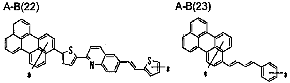
- Examples of the A-B moiety in formula (1) include A-B(1) to A-B(35) shown below.
- the ring structure at the left end corresponds to A, and the other part corresponds to B.
- each bond drawn across two or more rings means that any of the carbon atoms in these rings may form a bond (the same applies hereinafter).
- the hydrocarbon group of the optionally substituted hydrocarbon group represented by R1, R2, and R3 may be an aromatic hydrocarbon group, an aliphatic hydrocarbon group-substituted aromatic hydrocarbon group, an aliphatic hydrocarbon group, or the like.
- the aromatic hydrocarbon group may be phenyl, naphthyl, cyclohexylphenyl, biphenyl, terphenyl, fluorenyl, thiophenylphenyl, furanylphenyl, 2'-phenyl-propylphenyl, benzyl, naphthylmethyl, or the like.
- the aliphatic hydrocarbon group may be an aliphatic hydrocarbon group of 1 to 20 carbon atoms as described above for A.
- the aliphatic hydrocarbon group-substituted aromatic hydrocarbon group may be phenyl, naphthyl, benzyl or the like substituted with the aliphatic hydrocarbon group.
- hydrocarbon groups may be substituted with a substituent such as a fluorine atom, a chlorine atom, a bromine atom, an iodine atom, a cyano group, a nitro group, a hydroxyl group, a thiol group, or an -NR7R8 group, wherein R7 and R8 represent the same groups as R7 and R8 described above for B.
- a substituent such as a fluorine atom, a chlorine atom, a bromine atom, an iodine atom, a cyano group, a nitro group, a hydroxyl group, a thiol group, or an -NR7R8 group, wherein R7 and R8 represent the same groups as R7 and R8 described above for B.
- the optionally substituted hydrocarbonoxy group represented by R1, R2, and R3 may has an optionally substituted hydrocarbon moiety, which can be exemplified by the same groups as the optionally substituted hydrocarbon group represented by R1 described above, and an -O- moiety, which is interposed between the hydrocarbon moiety and the Si atom.
- At least one of R1, R2, and R3 represents an optionally substituted hydrocarbon oxy group.
- at least one of R1, R2, and R3 is an aliphatic hydrocarbonoxy group, or all of R1, R2, and R3 are optionally substituted hydrocarbonoxy groups.
- two or three of R1, R2, and R3 are each a linear or branched aliphatic hydrocarbonoxy group (especially of 1 to 5 carbon atoms), and none or one of them is a linear or branched aliphatic hydrocarbon group (especially of 1 to 5 carbon atoms).
- all of R1, R2, and R3 are each a linear or branched aliphatic hydrocarbonoxy group (especially of 1 to 5 carbon atoms).
- the optionally substituted hydrocarbon group represented by R4 and R5 may be the group described above for R1.
- R4 and R5 may be linked together to form a ring, or R4 and R5 may be each independently linked with A to form a ring.
- the partial structure (2) shown below is preferably any one of the partial structures (2-1) to (2-4) shown below, so that the compound can have particularly good properties for photoelectric conversion applications.
- the compound having the partial structure (2-1) or (2-2) shown below is particularly preferred because it is easy to produce and has high efficiency of electron injection into the support.
- the compound represented by formula (1) is preferably a compound having the partial structure (3-1) or (3-2) as the partial structure (3) shown below because such a compound is easy to produce and has good properties for photoelectric conversion applications.
- the compound represented by formula (1) preferably satisfies at least one of the following conditions (i) to (iii):
- the compound satisfying the condition (i) is preferable in that it has particularly high efficiency of electron injection into the support.
- the compound satisfying the condition (ii) is preferable in that it is easy to produce and that a particularly large number of moles of it can be adsorbed to the support.
- the compound satisfying the condition (iii) is preferable in that it can provide particularly high durability to photoelectric conversion devices.
- Me represents methyl, Et ethyl, Bu butyl, Pr propyl, Pen pentyl, Hex hexyl, Dec decyl, and Ph phenyl.
- the novel compound of the invention can be obtained by a method based on known or well-known general reactions, and the method for synthesizing it is not restricted.
- a typical example of the synthetic method includes allowing a halide (11) to react with a silylating agent (12) as shown in reaction formula (A) below, which enables the synthesis of the novel compound of the invention represented by formula (1).
- the catalyst, the ligand, and the base may be changed as needed.
- A, B, and R1 to R5 represent the same groups as those in formula (1), X represents a halogen atom, and dba represents a dibenzylideneacetone ligand.
- novel compound of the invention may be supported on a support, and such a support material carrying the novel compound of the invention is advantageously used in applications such as photoelectric conversion devices.
- the novel compound of the invention can also be used in other applications such as synthetic intermediates for optical recording materials, pharmaceuticals, agricultural chemicals, perfumes, dyes, etc.; a variety of functional materials and raw materials for polymers; photoelectrochemical cells, non-linear optical devices, electrochromic displays, holograms, organic semiconductors, and organic ELs; silver halide photographic materials, photosensitizers; colorants for use in printing ink, inkjet printing, electro-photographic color toners, cosmetics, and plastics; protein staining agents and luminescent dyes for use in detection of substances; and raw materials for synthetic quartz, paints, synthetic catalysts, catalyst supports, surface coating thin film materials, silicone rubber crosslinking agents, and thickening and binding agents.
- Examples of the material (support) for use in the support material of the invention include organic resins such as acrylic resins and fluororesins, metal oxides such as titanium oxide, zinc oxide, and aluminum oxide, silicon oxide, zeolite, activated carbon, etc, which preferably have a porous surface.
- the novel compound of the invention has high adsorption ability to a support because it has an alkoxysilyl group.
- the compound of the invention can be supported on a support using a known method such as gas-phase adsorption or liquid-phase adsorption.
- An example of liquid-phase adsorption includes dissolving the compound of the invention in a solvent and immersing the support in the solution so that the compound is adsorbed to the support.
- the support may be in any shape.
- the shape of the support may be appropriately selected from film shape, powdery shape, granular shape, or other shapes, depending on the intended use of the support.
- the size of the support and the amount of the compound of the invention supported on the support are also not restricted, and they may be appropriately selected depending on the intended use of the support.
- the support material of the invention carrying the novel compound of the invention can be advantageously used in the photoelectric conversion device described below and also be used for catalysts, toners, and other materials.
- the photoelectric conversion device of the invention is a dye-sensitized photoelectric conversion device, which may be the same as a conventional dye-sensitized photoelectric conversion device except that the novel compound of the invention is used therein as a dye.
- a typical example of the structure of the photoelectric conversion device of the invention will be described with reference to Figs. 1 and 2 .
- Fig. 1 schematically shows the cross-sectional structure of an example of the photoelectric conversion device of the invention.
- Fig. 2 extracts and shows in an enlarged manner the principal part of the photoelectric conversion device shown in Fig. 1 .
- the photoelectric conversion device shown in Figs. 1 and 2 corresponds to the principal part of what is called a dye-sensitized solar cell.
- the photoelectric conversion device has a working electrode 10 and a counter electrode 20, which are opposed to each other with an electrolyte-containing layer 30 interposed therebetween, in which at least one of the working electrode 10 and the counter electrode 20 is an optically-transparent electrode.
- the working electrode 10 includes a conductive substrate 11, a metal oxide semiconductor layer 12 provided on one surface (the counter electrode 20-side surface) of the substrate 11, and a dye 13 supported on the metal oxide semiconductor layer 12.
- the dye 13 corresponds to the novel compound of the invention represented by formula (1)
- the metal oxide semiconductor layer 12 carrying the dye (the novel compound of the invention) corresponds to the support material of the invention.
- the working electrode 10 functions as a negative electrode for the external circuit.
- the conductive substrate 11 includes an insulating substrate 11A and a conductive layer 11B provided on the surface of the substrate 11A.
- the substrate 11A may be made of an insulating material such as glass or plastic.
- plastic is used in the form of a transparent polymer film.
- plastic used to form a transparent polymer film include tetraacetyl cellulose (TAC), polyethylene terephthalate (PET), polyethylene naphthalate (PEN), syndiotactic polystyrene (SPS), polyphenylene sulfide (PPS), polycarbonate (PC), polyarylate (PAR), polysulfone (PSF), polyestersulfone (PES), polyetherimide (PEI), cyclic polyolefin, brominated phenoxy resin, etc.
- TAC tetraacetyl cellulose
- PET polyethylene terephthalate
- PEN polyethylene naphthalate
- SPS syndiotactic polystyrene
- PPS polyphenylene sulfide
- PC polycarbonate
- PAR polyarylate
- PES polys
- Examples of the conductive layer 11B include a conductive metal oxide thin film including indium oxide, tin oxide, indium-tin complex oxide (ITO), fluorine-doped tin oxide (FTO: F-SnO 2 ), or the like; a metal thin film including gold (Au), silver (Ag), platinum (Pt), or the like; and a layer made of a metal mesh, a conductive polymer, or the like.
- a conductive metal oxide thin film including indium oxide, tin oxide, indium-tin complex oxide (ITO), fluorine-doped tin oxide (FTO: F-SnO 2 ), or the like
- a metal thin film including gold (Au), silver (Ag), platinum (Pt), or the like
- a layer made of a metal mesh, a conductive polymer, or the like are examples of the conductive layer 11B.
- the conductive substrate 11 may be a monolayer structure made of a conductive material.
- the conductive substrate 11 is typically made of a conductive metal oxide such as indium oxide, tin oxide, indium-tin complex oxide, or fluorine-doped tin oxide, a metal such as gold, silver, or platinum, or a conductive polymer.
- the metal oxide semiconductor layer 12 is a support, on which the dye 13 is supported, and, for example, has a porous structure as shown in Fig. 2 .
- the metal oxide semiconductor layer 12 includes a dense layer 12A and a porous layer 12B.
- the dense layer 12A which is formed at the interface with the conductive substrate 11, is preferably dense and less-porous, more preferably in the form of a film.
- the porous layer 12B which is formed at the surface in contact with the electrolyte-containing layer 30, preferably has a structure with a large number of pores and a large surface area, and more preferably a porous structure made of deposited fine particles.
- the metal oxide semiconductor layer 12 may be formed to have a film-shaped monolayer structure.
- the term “carrying" or “supported on” refers to a state in which the dye 13 is chemically, physically, or electrically bonded or adsorbed to the porous layer 12B.
- the material (metal oxide semiconductor material) included in the metal oxide semiconductor layer 12 may be titanium oxide, zinc oxide, tin oxide, niobium oxide, indium oxide, zirconium oxide, tantalum oxide, vanadium oxide, yttrium oxide, aluminum oxide, or magnesium oxide. Titanium oxide and zinc oxide are particularly preferred as the metal oxide semiconductor material in that they can yield high conversion efficiency. Any of these metal oxide semiconductor materials may be used alone or in combination of two or more (as a mixture, a mixed crystal, a solid solution, a surface coating, or the like). For example, titanium oxide may be used in combination with zinc oxide or the like.
- the metal oxide semiconductor layer 12 having a porous structure may be formed using a method such as an electrolytic deposition technique, a coating technique, or a firing technique.
- a process of forming the metal oxide semiconductor layer 12 using an electrolytic deposition technique may include providing an electrolytic bath liquid containing fine particles of a metal oxide semiconductor material and depositing the fine particles on the conductive layer 11B of the conductive substrate 11 in the electrolytic bath liquid so that the metal oxide semiconductor material is precipitated thereon.
- a process of forming the metal oxide semiconductor layer 12 using a coating technique may include applying, to the conductive substrate 11, a dispersion (metal oxide slurry) containing dispersed fine particles of a metal oxide semiconductor material and then drying the applied dispersion to remove the dispersion medium from the dispersion.
- a process of forming the metal oxide semiconductor layer 12 using a firing technique may include applying a metal oxide slurry to the conductive substrate 11 in the same way as in the coating technique, drying the slurry, and then firing the dried material.
- a metal oxide slurry to the conductive substrate 11 in the same way as in the coating technique, drying the slurry, and then firing the dried material.
- a less heat-resistant plastic material or polymer film material can be used as the substrate 11A, so that a highly flexible electrode can be formed.
- the metal oxide semiconductor layer 12 may also be treated with an organic base, a urea derivative, or a cyclic sugar chain.
- organic base include diarylamine, triarylamine, pyridine, 4-tert-butylpyridine, polyvinyl pyridine, quinoline, piperidine, and amidine.
- the treatment may be performed before or after the dye 13 is adsorbed as described below.
- the treatment method may be an immersion treatment, and a solid treatment agent may be dissolved in an organic solvent and then be used for the immersion treatment.
- the novel compound of the invention represented by formula (1) corresponds to the dye 13.
- the ratio of the amount of electrons injected from the whole of the dye 13 into the metal oxide semiconductor layer 12 to the amount of applied light will be higher, so that the conversion efficiency will be higher.
- the dye 13 only has to include at least one novel compound of the invention represented by formula (1) and may include any other dye.
- any other dye include organic dyes (hereinafter referred to as other organic dyes) and organometallic complex compounds, and preferably include dyes having a group capable of adsorbing to the metal oxide semiconductor layer 12 (support).
- organic dyes examples include eosin Y, dibromofluorescein, fluorescein, rhodamine B, pyrogallol, dichlorofluorescein, Erythrosine B (Erythrosine is a registered trademark), fluorescin, mercurochrome, cyanine dyes, merocyanine disazo dyes, trisazo dyes, anthraquinone dyes, polycyclic quinone dyes, indigo dyes, diphenylmethane dyes, trimethylmethane dyes, quinoline dyes, benzophenone dyes, naphthoquinone dyes, perylene dyes, fluorenone dyes, squarylium dyes, azulenium dyes, perinone dyes, quinacridone dyes, metal-free phthalocyanine dyes, metal-free porphyrin dyres, or metal-free azaporphyrin dyes.
- organometallic complex compounds include organometallic complex compounds having both an ionic coordinate bond, which is formed between a metal cation and a nitrogen anion in an aromatic heterocyclic ring, and a nonionic coordinate bond, which is formed between a metal cation and a nitrogen atom or a chalcogen atom; and organometallic complex compounds having both an ionic coordinate bond, which is formed between a metal cation and an oxygen anion or a sulfur anion, and a nonionic coordinate bond, which is formed between a metal cation and a nitrogen atom or a chalcogen atom.
- metal phthalocyanine dyes such as copper phthalocyanine, titanyl phthalocyanine, cobalt phthalocyanine, nickel phthalocyanine, and iron phthalocyanine; metal naphthalocyanine dyes, metal porphyrin dyes, metal azaporphyrin dyes; and bipyridyl, terpyridyl, phenanthroline, bicinchoninate, azo, or quinolinol metal complexes with ruthenium, iron, or osmium, and other ruthenium complexes.
- metal phthalocyanine dyes such as copper phthalocyanine, titanyl phthalocyanine, cobalt phthalocyanine, nickel phthalocyanine, and iron phthalocyanine
- metal naphthalocyanine dyes such as copper phthalocyanine, titanyl phthalocyanine, cobalt phthalocyanine, nickel phthalocyanine, and iron phthalocyanine
- the dye 13 may also contain one or more additives.
- additives include association inhibitors capable of inhibiting the association of compounds in the dye, such as cholic acid compounds represented by chemical formula (13). Any of such additives may be used alone or in mixture of two or more.
- R91 represents an alkyl group having an acidic group
- R92 represents a group bonded to any of the carbon atoms of the steroid skeleton and selected from a hydroxyl group, a halogen group, an alkyl group, an alkoxy group, an aryl group, a heterocyclic group, an acyl group, an acyloxy group, an oxycarbonyl group, an oxo group, an acidic group, or a derivative of any of these groups
- R92 groups may be the same or different
- t represents an integer of 1 to 5
- any carbon-carbon bond in the steroid skeleton may be a single bond or a double bond.
- the counter electrode 20 includes a conductive substrate 21 and a conductive layer 22 provided on the substrate 21.
- the counter electrode 20 functions as a positive electrode for the external circuit.
- Examples of the material for the conductive substrate 21 may include those for the substrate 11A of the conductive substrate 11 in the working electrode 10.
- the conductive layer 22 includes one or more conductive materials and optionally a binder.
- the conductive material used to form the conductive layer 22 may be a metal such as platinum, gold, silver, copper (Cu), rhodium (Rh), ruthenium (Ru), aluminum (Al), magnesium (Mg), or indium (In), carbon (C), or a conductive polymer.
- the binder that may be used to form the conductive layer 22 may be acrylic resin, polyester resin, phenolic resin, epoxy resin, cellulose, melamine resin, fluoroelastomer, or polyimide resin.
- the counter electrode 20 may be a monolayer structure of the conductive layer 22.
- the electrolyte-containing layer 30 includes a redox electrolyte having a redox couple.
- the redox electrolyte may be an I - /I 3 - system, a Br - /Br 3 - system, a quinone/hydroquinone system, a Co complex system, or a nitroxy radical compound system.
- the redox electrolyte may be a combination of a halide salt and elementary halogen, such as a combination of an iodide salt and elementary iodine or a combination of a bromide salt and bromine.
- halide salt examples include cesium halide, quaternary alkyl ammonium halides, imidazolium halides, thiazolium halides, oxazolium halides, quinolinium halides, or pyridinium halides.
- iodide salts include cesium iodide, quaternary alkyl ammonium iodides such as tetraethyl ammonium iodide, tetrapropyl ammonium iodide, tetrabutyl ammonium iodide, tetrapentyl ammonium iodide, tetrahexyl ammonium iodide, tetraheptyl ammonium iodide, or trimethylphenyl ammonium iodide; imidazolium iodides such as 3-methylimidazolium iodide or 1-propyl-2,3-dimethylimidazolium iodide; thiazolium iodides such as 3-ethyl-2-methyl-2-thiazolium iodide, 3-ethyl-5-(2-hydroxyethyl)-4-methylthiazolium io
- bromide salts examples include quaternary alkyl ammonium bromide.
- the combination of a halide salt and elementary halogen is preferably a combination of at least one of the above iodide salts and elementary iodine.
- the redox electrolyte may a combination of an ionic liquid and elementary halogen.
- the redox electrolyte may further contain the halide salt or the like.
- the ionic liquid include those capable of being used in batteries or solar cells, such as those disclosed in publications such as Inorg. Chem. (1996), 35, pp. 1168-1178 , Electrochemistry (2002), 2, pp. 130-136 , Japanese Patent Application National Publication (Laid-Open) No. 09-507334 , or JP-A No. 08-259543 .
- the ionic liquid is preferably a salt having a melting point lower than room temperature (25°C) or a salt that can be liquefied at room temperature when dissolved with any other molten salt or the like although it has a melting point higher than room temperature.
- the ionic liquid include the anions and the cations shown below.
- ionic liquid cations include ammonium, imidazolium, oxazolium, thiazolium, oxadiazolium, triazolium, pyrrolidinium, pyridinium, piperidinium, pyrazolium, pyrimidinium, pyrazinium, triazinium, phosphonium, sulfonium, carbazolium, indolium, or a derivative of any of the above. Any of these cations may be used alone or in mixture of two or more. Specific examples include 1-methyl-3-propylimidazolium, 1-butyl-3-methylimidazolium, 1,2-dimethyl-3-propylimidazolium, and 1-ethyl-3-methylimidazolium.
- ionic liquid anions examples include metal chlorides such as AlCL 4 - and Al 2 Cl 7 - , fluorine-containing ions such as PF 6 - , BF 4 - , CF 3 SO 3 - , N(CF 3 SO 2 ) 2 - , F(HF) n - , and CF 3 COO - , fluorine-free compound ions such as NO 3 - , CH 3 COO - , C 6 H 11 COO - , CH 3 OSO 3 - , CH 3 OSO 2 - , CH 3 SO 3 - , CH 3 SO 2 - , (CH 3 O) 2 PO 2 - , N(CN) 2 - , and SCN - , and halide ions such as iodide ions, and bromide ions. Any of these ions may be used alone or in mixture of two or more.
- the ionic liquid anion is preferably an iodide ion.
- the electrolyte-containing layer 30 may be produced using a liquid electrolyte (electrolytic solution), which is a solution of the redox electrolyte in a solvent, or using a solid polymer electrolyte including an electrolytic solution contained in a polymer material.
- the electrolyte-containing layer 30 may be produced using a solidified (paste-like) electrolyte including a mixture of an electrolytic solution and a particulate carbon material such as carbon black.
- the carbon material-containing solidified electrolyte does not need to contain elementary halogen because the carbon material has the function of catalyzing the redox reaction.
- Such a redox electrolyte may contain one or more organic solvents in which the halide salt, the ionic liquid, or the like is soluble.
- organic solvent may be an electrochemically inert organic solvent, such as acetonitrile, propionitrile, butyronitrile, methoxyacetonitrile, 3-methoxypropionitrile, valeronitrile, dimethyl carbonate, ethyl methyl carbonate, ethylene carbonate, propylene carbonate, N-methylpyrrolidone, pentanol, quinoline, N,N-dimethylformamide, ⁇ -butyrolactone, dimethyl sulfoxide, or 1,4-dioxane.
- the electrolyte-containing layer 30 may also contain an additive such as an acyclic sugar ( JP-A No. 2005-093313 ), a pyridine compound ( JP-A No. 2003-331936 ), a urea derivative ( JP-A No.
- a gelling agent dibenzylidine-D-sorbitol, a cholesterol derivative, an amino acid derivative, an alkylamide derivative of trans-(1R,2R)-1,2-cyclohexanediamine, an alkyl urea derivative, N-octyl-D-gluconamide benzoate, an amphiphilic amino acid derivative, a quaternary ammonium derivative, the layered clay mineral disclosed in Japanese Patent No. 4692694 , or a photo-polymerizable monomer such as an acrylic acid monomer).
- a gelling agent dibenzylidine-D-sorbitol, a cholesterol derivative, an amino acid derivative, an alkylamide derivative of trans-(1R,2R)-1,2-cyclohexanediamine, an alkyl urea derivative, N-octyl-D-gluconamide benzoate, an amphiphilic amino acid derivative, a quaternary ammonium derivative, the layered clay mineral disclosed in Japanese Patent No. 469
- the dye 13 supported on the working electrode 10 in the photoelectric conversion device When the dye 13 supported on the working electrode 10 in the photoelectric conversion device is irradiated with light (sunlight, or ultraviolet light, visible light, or near infrared light equivalent to sunlight), the dye 13 is excited by absorbing the light to inject electrons into the metal oxide semiconductor layer 12. The electrons are transferred to the adjacent conductive layer 11B and then reach the counter electrode 20 via the external circuit.
- the electrolyte-containing layer 30 the electrolyte is oxidized so that the dye 13, which is oxidized with the electron transfer, can return (or be reduced) to its ground state. This oxidized electrolyte receives the above electrons.
- the electrons transfer between the working electrode 10 and the counter electrode 20 and the associated redox reaction in the electrolyte-containing layer 30 are repeated. This generates continuous transfer of electrons to enable steady photoelectric conversion.
- the photoelectric conversion device of the invention can be fabricated as described below.
- the working electrode 10 is first formed.
- the metal oxide semiconductor layer 12 having a porous structure is first formed on the conductive layer 11B-side surface of the conductive substrate 11 using an electrolytic deposition technique or a firing technique.
- an electrolytic deposition technique for example, an electrolyte bath containing a metal salt for forming a metal oxide semiconductor material is set to a predetermined temperature while the electrolyte bath is bubbled with oxygen or air, and the conductive substrate 11 is immersed in the electrolyte bath when a constant voltage is applied between the conductive substrate 11 and a counter electrode.
- the metal oxide semiconductor material is deposited on the conductive layer 11B so as to form a porous structure.
- the counter electrode may be shifted as needed in the electrolyte bath.
- a firing technique for example, a metal oxide slurry, which is prepared by dispersing a powder of a metal oxide semiconductor material in a dispersion medium, is applied to the conductive substrate 11, dried, and then fired to form a porous structure.
- the dye 13 including the novel compound of the invention represented by formula (1) is dissolved in an organic solvent to form a dye solution.
- the conductive substrate 11 with the metal oxide semiconductor layer 12 formed thereon is immersed in the dye solution so that the dye 13 is deposited (supported) on the metal oxide semiconductor layer 12.
- the concentration of the novel compound of the invention in the dye solution is preferably from 1.0 ⁇ 10 -5 to 1.0 ⁇ 10 -3 mol/dm 3 , more preferably 5.0 ⁇ 10 -5 to 5.0 ⁇ 10 -4 mol/dm 3 .
- the solvent used to form the dye solution may be of any type capable of dissolving the novel compound of the invention, examples of which include hydrocarbons such as toluene, benzene, and xylene; alcohols such as methanol, ethanol, and tert-butanol; ether alcohols such as methyl cellosolve, ethyl cellosolve, butyl cellosolve, and butyl diglycol; ketones such as acetone, methyl ethyl ketone, methyl isobutyl ketone, cyclohexanone, and diacetone alcohol; esters such as ethyl acetate, butyl acetate, and methoxyethyl acetate; acrylic esters such as ethyl acrylate and butyl acrylate; fluorinated alcohols such as 2,2,3,3,-tetrafluoropropanol; chlorinated hydrocarbons such as methylene dichloride, dichloroethane,
- the conductive layer 22 is formed on one side of the conductive substrate 21 to form the counter electrode 20.
- the conductive layer 22 is formed by sputtering of a conductive material.
- the dye 13-carrying surface of the working electrode 10 and the conductive layer 22-side surface of the counter electrode 20 are opposed to each other with a predetermined distance kept therebetween, and are fixed with a spacer (not shown) such as a sealant. And then, the whole is sealed, for example, except for the inlet for the electrolyte. Subsequently, the electrolyte is injected between the working electrode 10 and the counter electrode 20, and then the inlet is sealed, so that the electrolyte-containing layer 30 is formed.
- the photoelectric conversion device shown in Figs. 1 and 2 is completed.
- the dye 13 includes the compound of the invention represented by formula (1), and thus the dye 13 is prevented from leaching into the electrolyte-containing layer 30 from the support material (metal oxide semiconductor layer 12) carrying the dye 13, in contrast to cases where compounds other than the compound of the invention are used.
- the amount of the dye 13 supported on the metal oxide semiconductor layer 12 will not decrease, so that the amount of electrons injected from the dye 13 into the metal oxide semiconductor layer 12 will not decrease. Because of such an effect, the photoelectric conversion device of the invention can have higher durability.
- the electrolyte-containing layer 30 may be replaced by a solid charge-transfer layer.
- the solid charge-transfer layer has a solid material in which carrier transport takes part in electrical conduction.
- Such a material is preferably an electron transport material, a hole transport material, or the like.
- the hole transport material is preferably an aromatic amine or a triphenylene derivative.
- the hole transport material include organic conductive polymers such as oligothiophene compounds, polypyrrole, polyacetylene or derivatives thereof, poly(p-phenylene) or derivatives thereof, poly(p-phenylenevinylene) or derivatives thereof, polythienylene vinylene or derivatives thereof, polythiophene or derivatives thereof, polyaniline or derivatives thereof, and polytoluidine or derivatives thereof.
- a p-type inorganic compound semiconductor may be used as the hole transport material.
- the p-type inorganic compound semiconductor is preferably has a band gap of 2 eV or more, more preferably 2.5 eV or more.
- the p-type inorganic compound semiconductor must have an ionization potential smaller than that of the working electrode 10 to create conditions under which the holes from the dye can be reduced.
- the ionization potential is preferably in the range of 4.5 eV to 5.5 eV, more preferably in the range of 4.7 eV to 5.3 eV.
- the p-type inorganic compound semiconductor may be a monovalent copper compound semiconductor.
- the monovalent copper compound semiconductor include CuI, CuSCN, CuInSe 2 , Cu(In,Ga)Se 2 , CuGaSe 2 , Cu 2 O, CuS, CuGaS 2 , CuInS 2 , CuAlSe 2 , etc.
- Other examples of the p-type inorganic compound semiconductor include GaP, NiO, CoO, FeO, Bi 2 O 3 , MoO 2 , Cr 2 O 3 , etc.
- such a solid charge-transfer layer may be formed by a method of forming a solid charge-transfer layer directly on the working electrode 10, which may be followed by forming the counter electrode 20.
- the hole transport material including an organic conductive polymer can be introduced into the interior of the electrode by a technique such as vacuum deposition, casting, coating, spin coating, immersion, electrolytic polymerization, or photo-electrolytic polymerization.
- the solid inorganic compound can also be introduced into the interior of the electrode by a technique such as casting, coating, spin coating, immersion, or electroplating.
- Part of the solid charge-transfer layer formed as described above is preferably infiltrated into part of the pores of the porous structure of the metal oxide semiconductor layer 12 so that it can be in direct contact.
- the compound of the invention can also increase the conversion efficiency of the photoelectric conversion device having the solid charge-transfer layer in place of the electrolyte-containing layer 30.
- the photoelectric conversion device of the invention may be used not only in solar cell applications as described above but also in other applications.
- other applications include optical sensors, etc.
- Support materials according to the invention were prepared by the procedure described below using the compounds synthesized as described above.
- the conductive substrate 11 made of a 2.0 cm long, 1.5 cm wide, 1.1 mm thick conductive glass substrate (F-SnO 2 ). Subsequently, 70 ⁇ m thick masking tapes were bonded to the conductive substrate 11 so as to surround a 0.5 cm long, 0.5 cm wide square area, and 3 cm 3 of a metal oxide slurry was applied in uniform thickness to the square area and then dried.
- the metal oxide slurry used was a suspension of 10% by weight of titanium oxide powder (TiO 2 , Ti-Nanoxide D manufactured by Solaronix SA.) in water.
- the masking tapes were peeled off from the conductive substrate 11, and the substrate was fired at 450°C in an electric furnace, so that the metal oxide semiconductor layer 12 with a thickness of about 5 ⁇ m was formed.
- compound No. 1 was dissolved at a concentration of 3 ⁇ 10 -4 mol/dm 3 in toluene to form a dye solution.
- the conductive substrate 11 with the metal oxide semiconductor layer 12 formed thereon was immersed in the dye solution, so that the dye 13-carrying working electrode 10 was formed.
- Table 3 shows the amount of the supported dye (the absorbance (Abs.) of the dye at ⁇ max) after the immersion in the remover, as a measure of the resistance to removal, when the amount of the supported dye before the immersion in the remover is normalized as 100. It can be concluded that the closer to 100 the amount of the supported dye after the removal is, the higher the resistance to removal.
- the working electrode 10 carrying each dye was prepared using the same process as in Example 1, except that the metal slurry shown in Table 3 was used and that compound No. 1 was replaced by the compound shown in Table 3, and the resistance of the dye to removal was determined as in Example 1.
- the results are shown in Table 3.
- Zinc oxide powder (FINEX-50 manufactured by Sakai Chemical Industry Co., Ltd., 20 nm in average particle size) was used as ZnO for the metal slurry shown in Table 3.
Landscapes
- Chemical & Material Sciences (AREA)
- Engineering & Computer Science (AREA)
- Organic Chemistry (AREA)
- Materials Engineering (AREA)
- Power Engineering (AREA)
- Spectroscopy & Molecular Physics (AREA)
- Physics & Mathematics (AREA)
- Microelectronics & Electronic Packaging (AREA)
- Inorganic Chemistry (AREA)
- General Chemical & Material Sciences (AREA)
- Electrochemistry (AREA)
- Chemical Kinetics & Catalysis (AREA)
- Hybrid Cells (AREA)
- Photovoltaic Devices (AREA)
Abstract

Description
- The invention relates to novel compounds, support materials produced with the novel compounds, and photoelectric conversion devices produced with the support materials.
- Dyes have been widely used in a variety of technical fields. As an example in the field of photoelectric conversion devices such as solar cells, photosensitizing dyes are used in dye-sensitized photoelectric conversion devices. Such dye-sensitized photoelectric conversion devices are theoretically expected to have high efficiency and thought to be producible at a cost lower than that of traditional photoelectric conversion devices made with silicon semiconductors.
- A dye-sensitized photoelectric conversion device has an electrode including an oxide semiconductor as a support on which a dye is supported. In such a dye-sensitized photoelectric conversion device, the dye is excited by absorbing incident light, and the excited dye injects electrons into the support to cause photoelectric conversion.
- Techniques that have been studied to improve the conversion efficiency and durability of dye-sensitized photoelectric conversion devices include improvements in the dye-supporting ability of a support. Specifically, if physical or chemical adsorption ability of a dye to a support is increased, excited energy can be transferred with high efficiency from the dye to the support, and the dye can be prevented from leaching into the device (specifically, leaching into the electrolytic solution or the like). A technique of adding an anchor group such as a carboxylic acid group or a silanol group to dye molecules has been tried to improve the supporting ability (see Patent Literatures 1 to 3).
- Solar cells are one of the important applications of dye-sensitized photoelectric conversion devices. Such solar cells are required to have high durability because of the nature of the intended use, but known dyes and photoelectric conversion devices made with such dyes still have insufficient performance.
-
- Patent Literature 1: Japanese Patent Application Laid-Open (JP-A) No.
2008-063390 - Patent Literature 2:
JP-A No. 2010-027749 - Patent Literature 3:
JP-A No. 2011-026412 - It is therefore an object of the invention to provide a dye having a high ability to adsorb to a support, to provide a support material carrying such a dye, and to provide a photoelectric conversion device with high efficiency and high durability.
- As a result of earnest study, the inventors have found novel compounds having a specific structure and have completed the invention based on the finding that the object can be achieved with such novel compounds.
- Specifically, the invention provides a novel compound represented by formula (1) below.

- A represents an optionally substituted aromatic hydrocarbon ring group or an optionally substituted aromatic heterocyclic group,
- B represents a group comprising a chain of one to four pieces of one or more groups selected from groups represented by formulae (B-1) to (B-13) below,
- R1, R2, and R3 each represent an optionally substituted hydrocarbon group or an optionally substituted hydrocarbonoxy group,
- at least one of R1, R2, and R3 represents an optionally substituted hydrocarbonoxy group,
- R4 and R5 each represent an optionally substituted hydrocarbon group,
- R4 and R5 may be linked together to form a ring, and R4 and R5 may be each independently linked with A to form a ring,
- X represents S, O, or NR, wherein R represents an optionally substituted hydrocarbon group, and
- any hydrogen atom may be replaced by a fluorine atom, a chlorine atom, a bromine atom, an iodine atom, a cyano group, a nitro group, a hydroxyl group, a thiol group, an -NR7R8 group, or an optionally substituted aliphatic hydrocarbon group, wherein R7 and R8 each represent an optionally substituted hydrocarbon group.
- The invention also provides a support material including a support and the novel compound of formula (1) supported on the support.
- The invention also provides a photoelectric conversion device including an electrode having such a support material.
- The novel compound of the invention, which has an alkoxysilyl group, has a high ability to adsorb to a support. The compound and the photoelectric conversion device having the compound-carrying support material have high efficiency and high durability and are suitable for use in applications needed to have high durability, such as solar cells.
-
-
Fig. 1 is a schematic diagram showing the cross-sectional structure of an example of the photoelectric conversion device of the invention. -
Fig. 2 is an enlarged diagram of the principal part of the photoelectric conversion device of the invention shown inFig. 1 . - Hereinafter, the novel compound of the invention, the support material carrying the novel compound, and the photoelectric conversion device produced using the support material will be described with reference to preferred embodiments.
- First, the novel compound of the invention (hereinafter also referred to as the compound of the invention) will be described.
- In formula (1), the group represented by A is a divalent group which is an optionally substituted aromatic hydrocarbon ring group or an optionally substituted aromatic heterocyclic group.
- Examples of the aromatic hydrocarbon ring group include an unsubstituted aromatic hydrocarbon ring group, an aliphatic hydrocarbon group-substituted aromatic hydrocarbon ring group, etc. Examples of the aromatic heterocyclic group include an unsubstituted aromatic heterocyclic group, an aliphatic hydrocarbon group-substituted aromatic heterocyclic group, etc.
- Examples of the divalent unsubstituted aromatic hydrocarbon ring group include 1,2-phenylene, 1,3-phenylene, 1,4-phenylene, naphthalene-1,2-diyl, naphthalene-1,3-diyl, naphthalene-1,4-diyl, naphthalene-1,5-diyl, naphthalene-1,6-diyl, naphthalene-1,7-diyl, naphthalene-1,8-diyl, naphthalene-2,3-diyl, naphthalene-2,6-diyl, anthracene-1,4-diyl, anthracene-1,5-diyl, anthracene-1,10-diyl, anthracene-9,10-diyl, perylene-3,9-diyl, perylene-3,10-diyl, pyrene-1,6-diyl, pyrene-2,7-diyl, etc.
- For example, the aliphatic hydrocarbon group-substituted divalent aromatic hydrocarbon ring group may have one to three aliphatic hydrocarbon groups of 1 to 20 carbon atoms as substituents on the divalent unsubstituted aromatic hydrocarbon ring.
- Examples of the aliphatic hydrocarbon group of 1 to 20 carbon atoms include linear, branched, and cyclic alkyl groups such as methyl, ethyl, propyl, isopropyl, butyl, sec-butyl, tert-butyl, isobutyl, amyl, isoamyl, tert-amyl, hexyl, heptyl, isoheptyl, tert-heptyl, n-octyl, isooctyl, tert-octyl, nonyl, cyclopropyl, cyclobutyl, cyclopentyl, cyclohexyl, cycloheptyl, cyclooctyl, cyclononyl, and cyclodecyl. The aliphatic hydrocarbon group of 1 to 20 carbon atoms may be intervened by -O-, -COO-, -OCO-, -CO-, -S-, -SO-, -SO2-, -NR6-, -C=C-, or -C≡C-, wherein R6 is an aliphatic hydrocarbon group of 1 to 20 carbon atoms, which may be exemplified by the same groups as the above aliphatic hydrocarbon group of 1 to 20 carbon atoms. When the intervening group has one or more carbon atoms, the total number of carbon atoms, including those in the intervening group, is from 1 to 20.
- Examples of the divalent unsubstituted aromatic heterocyclic group include furan-2,5-diyl, furan-3,5-diyl, thiophene-2,5-diyl, thiophene-3,5-diyl, 2H-chromene-3,7-diyl, benzothiophene-2,6-diyl, benzothiophene-2,5-diyl, etc.
- Examples of the aliphatic hydrocarbon group-substituted divalent aromatic heterocyclic group include 1-alkyl-pyrrole-2,5-diyl, 1-alkyl-pyrrole-3,5-diyl, and a group having one to three aliphatic hydrocarbon groups of 1 to 20 carbon atoms as substituents on the divalent unsubstituted aromatic heterocyclic group. The aliphatic hydrocarbon group of 1 to 20 carbon atoms may be exemplified by the same groups as the above aliphatic hydrocarbon group of 1 to 20 carbon atoms.
- The aromatic hydrocarbon ring groups or the aromatic heterocyclic groups listed above may further have a substituent(s). The aromatic hydrocarbon ring groups and the aromatic heterocyclic groups may be substituted with groups such as a fluorine atom, a chlorine atom, a bromine atom, an iodine atom, a cyano group, a nitro group, a hydroxyl group, a thiol group, and an -NR7R8 group. R7 and R8 represent the same groups as represented by R7 and R8, respectively, in formulae (B-1) to (B-13) shown below. When the aromatic hydrocarbon ring group or the aromatic heterocyclic group has a methylene moiety, its two hydrogen atoms may be replaced by one oxygen atom to form carbonyl.
- In formula (1), B represents a group including a chain of one to four pieces of one or more groups selected from the groups represented by formulae (B-1) to (B-13), preferably a group including a chain of two to four pieces of one or more groups selected from the groups represented by formulae (B-1) to (B-13). Pieces of each group represented by any of formulae (B-1) to (B-13) may be linked in any direction. The mark * in the group represented by each of formulae (B-1) to (B-13) indicates the position to which the adjacent group is to be linked (the same applies hereinafter).
- In formulae (B-1) to (B-13), X represents S, O, or NR, wherein R represents an optionally substituted hydrocarbon group. Examples of the optionally substituted hydrocarbon group represented by R are the same as those of the optionally substituted hydrocarbon group represented by R1, R2, and R3 described below.
- Any hydrogen atom in the groups represented by formulae (B-1) to (B-13) may be replaced by a fluorine atom, a chlorine atom, a bromine atom, an iodine atom, a cyano group, a nitro group, a hydroxyl group, a thiol group, an -NR7R8 group, or an optionally substituted aliphatic hydrocarbon group, wherein R7 and R8 each represent an optionally substituted hydrocarbon group. Groups as substituents on each of the B groups may be linked together to form a ring.
- For example, the optionally substituted aliphatic hydrocarbon group may be the above aliphatic hydrocarbon group of 1 to 20 carbon atoms, and the groups may be substituted with the substituents listed above for the aromatic hydrocarbon ring group and the aromatic heterocyclic group.
- Examples of the optionally substituted hydrocarbon groups represented by R7 and R8 are the same as those of the optionally substituted hydrocarbon groups represented by R1, R2, and R3 described below.
- Examples of the A-B moiety in formula (1) include A-B(1) to A-B(35) shown below. In each of the examples of the A-B moiety shown below, the ring structure at the left end corresponds to A, and the other part corresponds to B.
- Although the examples shown below have no substituent, the A moiety may have a substituent(s) as mentioned above, and any hydrogen atom in the B moiety may be replaced by a substituent as mentioned above. In each of A-B(16) to A-B(23) shown below, each bond drawn across two or more rings means that any of the carbon atoms in these rings may form a bond (the same applies hereinafter).




- In formula (1), the hydrocarbon group of the optionally substituted hydrocarbon group represented by R1, R2, and R3 may be an aromatic hydrocarbon group, an aliphatic hydrocarbon group-substituted aromatic hydrocarbon group, an aliphatic hydrocarbon group, or the like.
- The aromatic hydrocarbon group may be phenyl, naphthyl, cyclohexylphenyl, biphenyl, terphenyl, fluorenyl, thiophenylphenyl, furanylphenyl, 2'-phenyl-propylphenyl, benzyl, naphthylmethyl, or the like. For example, the aliphatic hydrocarbon group may be an aliphatic hydrocarbon group of 1 to 20 carbon atoms as described above for A. The aliphatic hydrocarbon group-substituted aromatic hydrocarbon group may be phenyl, naphthyl, benzyl or the like substituted with the aliphatic hydrocarbon group.
- These hydrocarbon groups may be substituted with a substituent such as a fluorine atom, a chlorine atom, a bromine atom, an iodine atom, a cyano group, a nitro group, a hydroxyl group, a thiol group, or an -NR7R8 group, wherein R7 and R8 represent the same groups as R7 and R8 described above for B.
- In formula (1), the optionally substituted hydrocarbonoxy group represented by R1, R2, and R3 may has an optionally substituted hydrocarbon moiety, which can be exemplified by the same groups as the optionally substituted hydrocarbon group represented by R1 described above, and an -O- moiety, which is interposed between the hydrocarbon moiety and the Si atom.
- At least one of R1, R2, and R3 represents an optionally substituted hydrocarbon oxy group. In terms of the high ability to adsorb to the support described below, it is preferable that at least one of R1, R2, and R3 is an aliphatic hydrocarbonoxy group, or all of R1, R2, and R3 are optionally substituted hydrocarbonoxy groups. It is more preferable that two or three of R1, R2, and R3 are each a linear or branched aliphatic hydrocarbonoxy group (especially of 1 to 5 carbon atoms), and none or one of them is a linear or branched aliphatic hydrocarbon group (especially of 1 to 5 carbon atoms). It is most preferable that all of R1, R2, and R3 are each a linear or branched aliphatic hydrocarbonoxy group (especially of 1 to 5 carbon atoms).
- In formula (1), the optionally substituted hydrocarbon group represented by R4 and R5 may be the group described above for R1. R4 and R5 may be linked together to form a ring, or R4 and R5 may be each independently linked with A to form a ring.
- In the compound represented by formula (1), the partial structure (2) shown below is preferably any one of the partial structures (2-1) to (2-4) shown below, so that the compound can have particularly good properties for photoelectric conversion applications. The compound having the partial structure (2-1) or (2-2) shown below is particularly preferred because it is easy to produce and has high efficiency of electron injection into the support.
- In the partial structures (2) and (2-1) to (2-4) shown below, the bond of A to B is omitted. In the partial structures (2-1) to (2-4) shown below, any carbon atom of the aromatic hydrocarbon ring and the aromatic heterocyclic ring may form the bond of A to B.


- The compound represented by formula (1) is preferably a compound having the partial structure (3-1) or (3-2) as the partial structure (3) shown below because such a compound is easy to produce and has good properties for photoelectric conversion applications.
- In the partial structures (3), (3-1), and (3-2) shown below, the bond of B to the Si atom is omitted. In the partial structures (3-1) and (3-2), any carbon atom in the ring structure at the right end may form the bond of B to the Si atom.


- The compound represented by formula (1) preferably satisfies at least one of the following conditions (i) to (iii):
- (i) the group represented by B has at least one piece of the group represented by any one of formulae (B-1) to (B-9) and (B-11) to (B-13) shown above;
- (ii) R4 and R5 are each an optionally substituted hydrocarbon group of 1 to 12 carbon atoms; and
- (iii) at least one of R4 and R5 is linked with A to form a ring.
- The compound satisfying the condition (i) is preferable in that it has particularly high efficiency of electron injection into the support. The compound satisfying the condition (ii) is preferable in that it is easy to produce and that a particularly large number of moles of it can be adsorbed to the support. The compound satisfying the condition (iii) is preferable in that it can provide particularly high durability to photoelectric conversion devices.
- Specific examples of the compound represented by formula (1) include compounds Nos. 1 to 68 shown below. It will be understood that these compounds are non-limiting examples of the novel compound of the invention. In the formulae, Me represents methyl, Et ethyl, Bu butyl, Pr propyl, Pen pentyl, Hex hexyl, Dec decyl, and Ph phenyl.


- The novel compound of the invention can be obtained by a method based on known or well-known general reactions, and the method for synthesizing it is not restricted. A typical example of the synthetic method includes allowing a halide (11) to react with a silylating agent (12) as shown in reaction formula (A) below, which enables the synthesis of the novel compound of the invention represented by formula (1). The catalyst, the ligand, and the base may be changed as needed.

- In the formula, A, B, and R1 to R5 represent the same groups as those in formula (1), X represents a halogen atom, and dba represents a dibenzylideneacetone ligand.
- As described below, the novel compound of the invention may be supported on a support, and such a support material carrying the novel compound of the invention is advantageously used in applications such as photoelectric conversion devices. The novel compound of the invention can also be used in other applications such as synthetic intermediates for optical recording materials, pharmaceuticals, agricultural chemicals, perfumes, dyes, etc.; a variety of functional materials and raw materials for polymers; photoelectrochemical cells, non-linear optical devices, electrochromic displays, holograms, organic semiconductors, and organic ELs; silver halide photographic materials, photosensitizers; colorants for use in printing ink, inkjet printing, electro-photographic color toners, cosmetics, and plastics; protein staining agents and luminescent dyes for use in detection of substances; and raw materials for synthetic quartz, paints, synthetic catalysts, catalyst supports, surface coating thin film materials, silicone rubber crosslinking agents, and thickening and binding agents.
- Next, the support material of the invention carrying the novel compound of the invention will be described.
- Examples of the material (support) for use in the support material of the invention include organic resins such as acrylic resins and fluororesins, metal oxides such as titanium oxide, zinc oxide, and aluminum oxide, silicon oxide, zeolite, activated carbon, etc, which preferably have a porous surface. The novel compound of the invention has high adsorption ability to a support because it has an alkoxysilyl group. The compound of the invention can be supported on a support using a known method such as gas-phase adsorption or liquid-phase adsorption. An example of liquid-phase adsorption includes dissolving the compound of the invention in a solvent and immersing the support in the solution so that the compound is adsorbed to the support.
- The support may be in any shape. For example, the shape of the support may be appropriately selected from film shape, powdery shape, granular shape, or other shapes, depending on the intended use of the support. The size of the support and the amount of the compound of the invention supported on the support are also not restricted, and they may be appropriately selected depending on the intended use of the support.
- The support material of the invention carrying the novel compound of the invention can be advantageously used in the photoelectric conversion device described below and also be used for catalysts, toners, and other materials.
- Next, the photoelectric conversion device of the invention will be described.
The photoelectric conversion device of the invention is a dye-sensitized photoelectric conversion device, which may be the same as a conventional dye-sensitized photoelectric conversion device except that the novel compound of the invention is used therein as a dye. Hereinafter, a typical example of the structure of the photoelectric conversion device of the invention will be described with reference toFigs. 1 and 2 . -
Fig. 1 schematically shows the cross-sectional structure of an example of the photoelectric conversion device of the invention.Fig. 2 extracts and shows in an enlarged manner the principal part of the photoelectric conversion device shown inFig. 1 . The photoelectric conversion device shown inFigs. 1 and 2 corresponds to the principal part of what is called a dye-sensitized solar cell. The photoelectric conversion device has a workingelectrode 10 and acounter electrode 20, which are opposed to each other with an electrolyte-containinglayer 30 interposed therebetween, in which at least one of the workingelectrode 10 and thecounter electrode 20 is an optically-transparent electrode. - For example, the working
electrode 10 includes aconductive substrate 11, a metaloxide semiconductor layer 12 provided on one surface (the counter electrode 20-side surface) of thesubstrate 11, and adye 13 supported on the metaloxide semiconductor layer 12. In the photoelectric conversion device of the invention, thedye 13 corresponds to the novel compound of the invention represented by formula (1), and the metaloxide semiconductor layer 12 carrying the dye (the novel compound of the invention) corresponds to the support material of the invention. - The working
electrode 10 functions as a negative electrode for the external circuit. For example, theconductive substrate 11 includes an insulatingsubstrate 11A and aconductive layer 11B provided on the surface of thesubstrate 11A. - For example, the
substrate 11A may be made of an insulating material such as glass or plastic. For example, plastic is used in the form of a transparent polymer film. Examples of plastic used to form a transparent polymer film include tetraacetyl cellulose (TAC), polyethylene terephthalate (PET), polyethylene naphthalate (PEN), syndiotactic polystyrene (SPS), polyphenylene sulfide (PPS), polycarbonate (PC), polyarylate (PAR), polysulfone (PSF), polyestersulfone (PES), polyetherimide (PEI), cyclic polyolefin, brominated phenoxy resin, etc. - Examples of the
conductive layer 11B include a conductive metal oxide thin film including indium oxide, tin oxide, indium-tin complex oxide (ITO), fluorine-doped tin oxide (FTO: F-SnO2), or the like; a metal thin film including gold (Au), silver (Ag), platinum (Pt), or the like; and a layer made of a metal mesh, a conductive polymer, or the like. - Alternatively, for example, the
conductive substrate 11 may be a monolayer structure made of a conductive material. In this case, theconductive substrate 11 is typically made of a conductive metal oxide such as indium oxide, tin oxide, indium-tin complex oxide, or fluorine-doped tin oxide, a metal such as gold, silver, or platinum, or a conductive polymer. - The metal
oxide semiconductor layer 12 is a support, on which thedye 13 is supported, and, for example, has a porous structure as shown inFig. 2 . The metaloxide semiconductor layer 12 includes adense layer 12A and aporous layer 12B. Thedense layer 12A, which is formed at the interface with theconductive substrate 11, is preferably dense and less-porous, more preferably in the form of a film. Theporous layer 12B, which is formed at the surface in contact with the electrolyte-containinglayer 30, preferably has a structure with a large number of pores and a large surface area, and more preferably a porous structure made of deposited fine particles. Alternatively, for example, the metaloxide semiconductor layer 12 may be formed to have a film-shaped monolayer structure. As used herein, the term "carrying" or "supported on" refers to a state in which thedye 13 is chemically, physically, or electrically bonded or adsorbed to theporous layer 12B. - For example, the material (metal oxide semiconductor material) included in the metal
oxide semiconductor layer 12 may be titanium oxide, zinc oxide, tin oxide, niobium oxide, indium oxide, zirconium oxide, tantalum oxide, vanadium oxide, yttrium oxide, aluminum oxide, or magnesium oxide. Titanium oxide and zinc oxide are particularly preferred as the metal oxide semiconductor material in that they can yield high conversion efficiency. Any of these metal oxide semiconductor materials may be used alone or in combination of two or more (as a mixture, a mixed crystal, a solid solution, a surface coating, or the like). For example, titanium oxide may be used in combination with zinc oxide or the like. - The metal
oxide semiconductor layer 12 having a porous structure may be formed using a method such as an electrolytic deposition technique, a coating technique, or a firing technique. A process of forming the metaloxide semiconductor layer 12 using an electrolytic deposition technique may include providing an electrolytic bath liquid containing fine particles of a metal oxide semiconductor material and depositing the fine particles on theconductive layer 11B of theconductive substrate 11 in the electrolytic bath liquid so that the metal oxide semiconductor material is precipitated thereon. A process of forming the metaloxide semiconductor layer 12 using a coating technique may include applying, to theconductive substrate 11, a dispersion (metal oxide slurry) containing dispersed fine particles of a metal oxide semiconductor material and then drying the applied dispersion to remove the dispersion medium from the dispersion. A process of forming the metaloxide semiconductor layer 12 using a firing technique may include applying a metal oxide slurry to theconductive substrate 11 in the same way as in the coating technique, drying the slurry, and then firing the dried material. Especially when an electrolytic deposition technique or a coating technique is used to form the metaloxide semiconductor layer 12, a less heat-resistant plastic material or polymer film material can be used as thesubstrate 11A, so that a highly flexible electrode can be formed. - The metal
oxide semiconductor layer 12 may also be treated with an organic base, a urea derivative, or a cyclic sugar chain. Examples of the organic base include diarylamine, triarylamine, pyridine, 4-tert-butylpyridine, polyvinyl pyridine, quinoline, piperidine, and amidine. The treatment may be performed before or after thedye 13 is adsorbed as described below. The treatment method may be an immersion treatment, and a solid treatment agent may be dissolved in an organic solvent and then be used for the immersion treatment. - The
dye 13, which is typically adsorbed to the metaloxide semiconductor layer 12, includes one or more dyes (sensitizing dyes) capable of injecting electrons into the metaloxide semiconductor layer 12 when excited by absorbing light. In the photoelectric conversion device of the invention, the novel compound of the invention represented by formula (1) corresponds to thedye 13. When the novel compound of the invention is used as thedye 13, the ratio of the amount of electrons injected from the whole of thedye 13 into the metaloxide semiconductor layer 12 to the amount of applied light will be higher, so that the conversion efficiency will be higher. - The
dye 13 only has to include at least one novel compound of the invention represented by formula (1) and may include any other dye. Examples of any other dye include organic dyes (hereinafter referred to as other organic dyes) and organometallic complex compounds, and preferably include dyes having a group capable of adsorbing to the metal oxide semiconductor layer 12 (support). - Examples of other organic dyes include eosin Y, dibromofluorescein, fluorescein, rhodamine B, pyrogallol, dichlorofluorescein, Erythrosine B (Erythrosine is a registered trademark), fluorescin, mercurochrome, cyanine dyes, merocyanine disazo dyes, trisazo dyes, anthraquinone dyes, polycyclic quinone dyes, indigo dyes, diphenylmethane dyes, trimethylmethane dyes, quinoline dyes, benzophenone dyes, naphthoquinone dyes, perylene dyes, fluorenone dyes, squarylium dyes, azulenium dyes, perinone dyes, quinacridone dyes, metal-free phthalocyanine dyes, metal-free porphyrin dyres, or metal-free azaporphyrin dyes.
- Examples of organometallic complex compounds include organometallic complex compounds having both an ionic coordinate bond, which is formed between a metal cation and a nitrogen anion in an aromatic heterocyclic ring, and a nonionic coordinate bond, which is formed between a metal cation and a nitrogen atom or a chalcogen atom; and organometallic complex compounds having both an ionic coordinate bond, which is formed between a metal cation and an oxygen anion or a sulfur anion, and a nonionic coordinate bond, which is formed between a metal cation and a nitrogen atom or a chalcogen atom. Specific examples include metal phthalocyanine dyes such as copper phthalocyanine, titanyl phthalocyanine, cobalt phthalocyanine, nickel phthalocyanine, and iron phthalocyanine; metal naphthalocyanine dyes, metal porphyrin dyes, metal azaporphyrin dyes; and bipyridyl, terpyridyl, phenanthroline, bicinchoninate, azo, or quinolinol metal complexes with ruthenium, iron, or osmium, and other ruthenium complexes.
- In addition to the above dye, the
dye 13 may also contain one or more additives. Examples of such additives include association inhibitors capable of inhibiting the association of compounds in the dye, such as cholic acid compounds represented by chemical formula (13). Any of such additives may be used alone or in mixture of two or more. -

- For example, the
counter electrode 20 includes a conductive substrate 21 and aconductive layer 22 provided on the substrate 21. Thecounter electrode 20 functions as a positive electrode for the external circuit. Examples of the material for the conductive substrate 21 may include those for thesubstrate 11A of theconductive substrate 11 in the workingelectrode 10. Theconductive layer 22 includes one or more conductive materials and optionally a binder. For example, the conductive material used to form theconductive layer 22 may be a metal such as platinum, gold, silver, copper (Cu), rhodium (Rh), ruthenium (Ru), aluminum (Al), magnesium (Mg), or indium (In), carbon (C), or a conductive polymer. For example, the binder that may be used to form theconductive layer 22 may be acrylic resin, polyester resin, phenolic resin, epoxy resin, cellulose, melamine resin, fluoroelastomer, or polyimide resin. Alternatively, for example, thecounter electrode 20 may be a monolayer structure of theconductive layer 22. - For example, the electrolyte-containing
layer 30 includes a redox electrolyte having a redox couple. For example, the redox electrolyte may be an I-/I3 - system, a Br-/Br3 - system, a quinone/hydroquinone system, a Co complex system, or a nitroxy radical compound system. More specifically, the redox electrolyte may be a combination of a halide salt and elementary halogen, such as a combination of an iodide salt and elementary iodine or a combination of a bromide salt and bromine. Examples of such a halide salt include cesium halide, quaternary alkyl ammonium halides, imidazolium halides, thiazolium halides, oxazolium halides, quinolinium halides, or pyridinium halides. Specific examples of the iodide salts include cesium iodide, quaternary alkyl ammonium iodides such as tetraethyl ammonium iodide, tetrapropyl ammonium iodide, tetrabutyl ammonium iodide, tetrapentyl ammonium iodide, tetrahexyl ammonium iodide, tetraheptyl ammonium iodide, or trimethylphenyl ammonium iodide; imidazolium iodides such as 3-methylimidazolium iodide or 1-propyl-2,3-dimethylimidazolium iodide; thiazolium iodides such as 3-ethyl-2-methyl-2-thiazolium iodide, 3-ethyl-5-(2-hydroxyethyl)-4-methylthiazolium iodide, or 3-ethyl-2-methylbenzothiazolium iodide; oxazolium iodides such as 3-ethyl-2-methyl-benzoxazolium iodide; quinolinium iodides such as 1-ethyl-2-methylquinolinium iodide; and pyridinium iodides. Examples of the bromide salts include quaternary alkyl ammonium bromide. The combination of a halide salt and elementary halogen is preferably a combination of at least one of the above iodide salts and elementary iodine. - Alternatively, for example, the redox electrolyte may a combination of an ionic liquid and elementary halogen. In this case, the redox electrolyte may further contain the halide salt or the like. Examples of the ionic liquid include those capable of being used in batteries or solar cells, such as those disclosed in publications such as Inorg. Chem. (1996), 35, pp. 1168-1178, Electrochemistry (2002), 2, pp. 130-136, Japanese Patent Application National Publication (Laid-Open) No.
09-507334 JP-A No. 08-259543 - Examples of ionic liquid cations include ammonium, imidazolium, oxazolium, thiazolium, oxadiazolium, triazolium, pyrrolidinium, pyridinium, piperidinium, pyrazolium, pyrimidinium, pyrazinium, triazinium, phosphonium, sulfonium, carbazolium, indolium, or a derivative of any of the above. Any of these cations may be used alone or in mixture of two or more. Specific examples include 1-methyl-3-propylimidazolium, 1-butyl-3-methylimidazolium, 1,2-dimethyl-3-propylimidazolium, and 1-ethyl-3-methylimidazolium.
- Examples of ionic liquid anions include metal chlorides such as AlCL4 - and Al2Cl7 -, fluorine-containing ions such as PF6 -, BF4 -, CF3SO3 -, N(CF3SO2)2 -, F(HF)n -, and CF3COO-, fluorine-free compound ions such as NO3 -, CH3COO-, C6H11COO-, CH3OSO3 -, CH3OSO2 -, CH3SO3 -, CH3SO2 -, (CH3O)2PO2 -, N(CN)2 -, and SCN-, and halide ions such as iodide ions, and bromide ions. Any of these ions may be used alone or in mixture of two or more. In particular, the ionic liquid anion is preferably an iodide ion.
- The electrolyte-containing
layer 30 may be produced using a liquid electrolyte (electrolytic solution), which is a solution of the redox electrolyte in a solvent, or using a solid polymer electrolyte including an electrolytic solution contained in a polymer material. Alternatively, the electrolyte-containinglayer 30 may be produced using a solidified (paste-like) electrolyte including a mixture of an electrolytic solution and a particulate carbon material such as carbon black. The carbon material-containing solidified electrolyte does not need to contain elementary halogen because the carbon material has the function of catalyzing the redox reaction. Such a redox electrolyte may contain one or more organic solvents in which the halide salt, the ionic liquid, or the like is soluble. Such an organic solvent may be an electrochemically inert organic solvent, such as acetonitrile, propionitrile, butyronitrile, methoxyacetonitrile, 3-methoxypropionitrile, valeronitrile, dimethyl carbonate, ethyl methyl carbonate, ethylene carbonate, propylene carbonate, N-methylpyrrolidone, pentanol, quinoline, N,N-dimethylformamide, γ-butyrolactone, dimethyl sulfoxide, or 1,4-dioxane. - For an improvement in the generating efficiency or durability of the photoelectric conversion device or other purposes, the electrolyte-containing
layer 30 may also contain an additive such as an acyclic sugar (JP-A No. 2005-093313 JP-A No. 2003-331936 JP-A No. 2003-168493 4692694 - When the
dye 13 supported on the workingelectrode 10 in the photoelectric conversion device is irradiated with light (sunlight, or ultraviolet light, visible light, or near infrared light equivalent to sunlight), thedye 13 is excited by absorbing the light to inject electrons into the metaloxide semiconductor layer 12. The electrons are transferred to the adjacentconductive layer 11B and then reach thecounter electrode 20 via the external circuit. On the other hand, in the electrolyte-containinglayer 30, the electrolyte is oxidized so that thedye 13, which is oxidized with the electron transfer, can return (or be reduced) to its ground state. This oxidized electrolyte receives the above electrons. Thus, the electrons transfer between the workingelectrode 10 and thecounter electrode 20 and the associated redox reaction in the electrolyte-containinglayer 30 are repeated. This generates continuous transfer of electrons to enable steady photoelectric conversion. - For example, the photoelectric conversion device of the invention can be fabricated as described below.
- The working
electrode 10 is first formed. The metaloxide semiconductor layer 12 having a porous structure is first formed on theconductive layer 11B-side surface of theconductive substrate 11 using an electrolytic deposition technique or a firing technique. When the metaloxide semiconductor layer 12 is formed using an electrolytic deposition technique, for example, an electrolyte bath containing a metal salt for forming a metal oxide semiconductor material is set to a predetermined temperature while the electrolyte bath is bubbled with oxygen or air, and theconductive substrate 11 is immersed in the electrolyte bath when a constant voltage is applied between theconductive substrate 11 and a counter electrode. In this process, the metal oxide semiconductor material is deposited on theconductive layer 11B so as to form a porous structure. In this process, the counter electrode may be shifted as needed in the electrolyte bath. When the metaloxide semiconductor layer 12 is formed using a firing technique, for example, a metal oxide slurry, which is prepared by dispersing a powder of a metal oxide semiconductor material in a dispersion medium, is applied to theconductive substrate 11, dried, and then fired to form a porous structure. Subsequently, thedye 13 including the novel compound of the invention represented by formula (1) is dissolved in an organic solvent to form a dye solution. Theconductive substrate 11 with the metaloxide semiconductor layer 12 formed thereon is immersed in the dye solution so that thedye 13 is deposited (supported) on the metaloxide semiconductor layer 12. - The concentration of the novel compound of the invention in the dye solution is preferably from 1.0 × 10⁻⁵ to 1.0 × 10⁻³ mol/dm3, more preferably 5.0 × 10⁻⁵ to 5.0 × 10⁻⁴ mol/dm3. The solvent used to form the dye solution may be of any type capable of dissolving the novel compound of the invention, examples of which include hydrocarbons such as toluene, benzene, and xylene; alcohols such as methanol, ethanol, and tert-butanol; ether alcohols such as methyl cellosolve, ethyl cellosolve, butyl cellosolve, and butyl diglycol; ketones such as acetone, methyl ethyl ketone, methyl isobutyl ketone, cyclohexanone, and diacetone alcohol; esters such as ethyl acetate, butyl acetate, and methoxyethyl acetate; acrylic esters such as ethyl acrylate and butyl acrylate; fluorinated alcohols such as 2,2,3,3,-tetrafluoropropanol; chlorinated hydrocarbons such as methylene dichloride, dichloroethane, and chloroform; and acetonitrile. Any of these organic solvents may be mixed together as desired. Toluene and acetonitrile are preferred.
- Subsequently, the
conductive layer 22 is formed on one side of the conductive substrate 21 to form thecounter electrode 20. For example, theconductive layer 22 is formed by sputtering of a conductive material. - Finally, the dye 13-carrying surface of the working
electrode 10 and the conductive layer 22-side surface of thecounter electrode 20 are opposed to each other with a predetermined distance kept therebetween, and are fixed with a spacer (not shown) such as a sealant. And then, the whole is sealed, for example, except for the inlet for the electrolyte. Subsequently, the electrolyte is injected between the workingelectrode 10 and thecounter electrode 20, and then the inlet is sealed, so that the electrolyte-containinglayer 30 is formed. Thus, the photoelectric conversion device shown inFigs. 1 and 2 is completed. - In the photoelectric conversion device of the invention, the
dye 13 includes the compound of the invention represented by formula (1), and thus thedye 13 is prevented from leaching into the electrolyte-containinglayer 30 from the support material (metal oxide semiconductor layer 12) carrying thedye 13, in contrast to cases where compounds other than the compound of the invention are used. Thus, the amount of thedye 13 supported on the metaloxide semiconductor layer 12 will not decrease, so that the amount of electrons injected from thedye 13 into the metaloxide semiconductor layer 12 will not decrease. Because of such an effect, the photoelectric conversion device of the invention can have higher durability. - Although the photoelectric conversion device described above has the electrolyte-containing
layer 30 between the workingelectrode 10 and thecounter electrode 20, the electrolyte-containinglayer 30 may be replaced by a solid charge-transfer layer. In this case, for example, the solid charge-transfer layer has a solid material in which carrier transport takes part in electrical conduction. Such a material is preferably an electron transport material, a hole transport material, or the like. - The hole transport material is preferably an aromatic amine or a triphenylene derivative. Examples of the hole transport material include organic conductive polymers such as oligothiophene compounds, polypyrrole, polyacetylene or derivatives thereof, poly(p-phenylene) or derivatives thereof, poly(p-phenylenevinylene) or derivatives thereof, polythienylene vinylene or derivatives thereof, polythiophene or derivatives thereof, polyaniline or derivatives thereof, and polytoluidine or derivatives thereof.
- Alternatively, for example, a p-type inorganic compound semiconductor may be used as the hole transport material. The p-type inorganic compound semiconductor is preferably has a band gap of 2 eV or more, more preferably 2.5 eV or more. The p-type inorganic compound semiconductor must have an ionization potential smaller than that of the working
electrode 10 to create conditions under which the holes from the dye can be reduced. Although the preferred range of the ionization potential of the p-type inorganic compound semiconductor varies with the dye used, the ionization potential is preferably in the range of 4.5 eV to 5.5 eV, more preferably in the range of 4.7 eV to 5.3 eV. - For example, the p-type inorganic compound semiconductor may be a monovalent copper compound semiconductor. Examples of the monovalent copper compound semiconductor include CuI, CuSCN, CuInSe2, Cu(In,Ga)Se2, CuGaSe2, Cu2O, CuS, CuGaS2, CuInS2, CuAlSe2, etc. Other examples of the p-type inorganic compound semiconductor include GaP, NiO, CoO, FeO, Bi2O3, MoO2, Cr2O3, etc.
- For example, such a solid charge-transfer layer may be formed by a method of forming a solid charge-transfer layer directly on the working
electrode 10, which may be followed by forming thecounter electrode 20. - For example, the hole transport material including an organic conductive polymer can be introduced into the interior of the electrode by a technique such as vacuum deposition, casting, coating, spin coating, immersion, electrolytic polymerization, or photo-electrolytic polymerization. The solid inorganic compound can also be introduced into the interior of the electrode by a technique such as casting, coating, spin coating, immersion, or electroplating. Part of the solid charge-transfer layer formed as described above (especially having a hole transport material) is preferably infiltrated into part of the pores of the porous structure of the metal
oxide semiconductor layer 12 so that it can be in direct contact. - As in the case that the electrolyte-containing
layer 30 is provided, the compound of the invention can also increase the conversion efficiency of the photoelectric conversion device having the solid charge-transfer layer in place of the electrolyte-containinglayer 30. - The photoelectric conversion device of the invention may be used not only in solar cell applications as described above but also in other applications. For example, other applications include optical sensors, etc.
- Hereinafter, the invention is more specifically described with reference to synthesis examples, examples, and comparative examples, which however are not intended to limit the invention.
- The synthesis examples below show the synthesis of compound Nos. 1 to 25 and 66 to 68 listed above. Halides as precursors and silylating agents (corresponding to chemical formulae (11) and (12) above, respectively) were purchased or synthesized by known methods.
- Mixed were 4-(4-bromophenylazo)-N,N-dimethylaniline (halide, 2.0 mmol, 0.60 g), triethoxysilane (silylating agent, 3.0 mmol, 0.49 g), tris(dibenzylidineacetone)dipalladium (0.03 mmol, 0.027 g), (2-biphenyl)di-tert-butylphosphine (0.12 mmol, 0.036 g), N,N-diisopropylethylamine (6.0 mmol, 0.78 g), and dimethylformamide (4 ml), and stirred at 60°C for 3 hours. After the reaction solution was cooled to room temperature, chloroform (10 ml) and water (10 ml) were added to the reaction solution, and oil-water separation was performed. The resultant organic layer was purified using PLC (with a eluent of hexane : ethyl acetate = 15 : 1) to yield 0.35 g of a yellow solid (yield 45.2%). The resultant solid was identified as compound No. 1 using UV-VIS (λmax) and 1H-NMR. The data are shown in Tables 1 and 2.
- Compound Nos. 2 to 25 and 66 to 68 were synthesized using the same method as in Synthesis Example 1, except that halides (bromides) and silylating agents suitable for the desired compounds were used instead. The appearance and yield of each resultant solid or liquid are shown in Table 1. The eluent used in the PLC purification depends on the compound and therefore is also shown in Table 1. The synthesized compounds were each identified as the desired compound in the same way as in Synthesis Example 1. The data are shown in Tables 1 and 2.
[Table 1] Compound Eluent Appearance Yield (%) λmax (nm) Synthesis Example 1 No. 1 HEX:AcOEt=15:1 Yellow solid 45 421(MeOH) Synthesis Example 2 No. 2 HEX:AcOEt=20:1 Yellow solid 11 421(MeOH) Synthesis Example 3 No. 3 HEX:AcOEt=10:1 Yellow solid 21 444(MeOH) Synthesis Example 4 No. 4 HEX:AcOEt=20:1 Yellow solid 15 416(MeOH) Synthesis Example 5 No. 5 HEX:AcOEt=20:1 Yellow solid 6 415(MeOH) Synthesis Example 6 No. 6 HEX:AcOEt=10:1 Yellow solid 19 418(MeOH) Synthesis Example 7 No. 7 HEX:AcOEt=1:1 Orange solid 26 448(MeOH) Synthesis Example 8 No. 8 HEX:AcOEt=10:1 Orange solid 30 456(MeOH) Synthesis Example 9 No. 9 HEX:CHCl3=1:1 Orange oil 10 443(CHCl3) Synthesis Example 10 No. 10 CHCl3 Orange solid 28 461(MeOH) Synthesis Example 11 No. 11 CHCl3 Orange solid 57 452(MeOH) Synthesis Example 12 No. 12 CHCl3 Orange solid 25 474(MeOH) Synthesis Example 13 No. 13 HEX:AcOEt=5:1 Yellow solid 11 428(CHCl3) Synthesis Example 14 No. 14 HEX:AcOEt=5:1 Orange solid 41 455(CHCl3) Synthesis Example 15 No. 15 CHCl3 Orange solid 34 486(CHCl3) Synthesis Example 16 No. 16 CHCl3 Orange solid 30 482(CHCl3) Synthesis Example 17 No. 17 HEX:AcOEt=1:1 Orange solid 15 476(MeOH) Synthesis Example 18 No. 18 HEX:AcOEt=10:1 Orange solid 11 453(MeOH) Synthesis Example 19 No. 19 HEX:AcOEt=10:1 Orange solid 1 453(CHCl3) Synthesis Example 20 No. 20 HEX:AcOEt=10:1 Orange solid 16 448(CHCl3) Synthesis Example 21 No. 21 CHCl3 Orange solid 2 490(CHCl3) Synthesis Example 22 No. 22 HEX:AcOEt=20:1 Yellow oil 21 407(CHCl3) Synthesis Example 23 No. 23 HEX:AcOEt=20:1 Yellow oil 35 366(CHCl3) Synthesis Example 24 No. 24 HEX:AcOEt=20:1 Yellow oil 26 407(CHCl3) Synthesis Example 25 No. 25 HEX:AcOEt=10:1 Yellow solid 36 385(CHCl3) Synthesis Example 26 No. 66 HEX:AcOEt=3:1 Yellow oil 14 411(CHCl3) Synthesis Example 27 No. 67 CHCl3 Orange solid 11 463(CHCl3) Synthesis Example 28 No. 68 CHCl3 Orange solid 14 467(CHCl3) HEX: hexane
AcOEt: ethyl acetate[Table 2-1] <1H-NMR ; CDCl3> Compound δ/ppm (proton number, multiplicity) Synthesis Example 1 No.1 7.90 (d, 2H), 7.84-7.78 (m, 4H), 6.77 (d, 2H), 3.90 (q, 4H), 3.11 (s, 6H), 1.27 (t, 6H) Synthesis Example 2 No.2 7.89 (d, 2H), 7.83-7.77 (m, 4H), 7.69 (d, 2H), 7.44-7.37 (m, 3H), 6.76 (d, 2H), 3.90 (q, 4H), 3.10 (s, 6H), 1.28 (t, 6H) Synthesis Example 3 No.3 7.87 (d, 2H), 7.83 (d, 2H), 7.36 (d, 1H), 7.32 (d, 1H), 7.17 (d, 1H), 7.04 (d, 1H), 6.76 (d, 2H), 3.91 (q, 6H), 3.10 (s, 6H), 1.28 (t, 9H) Synthesis Example 4 No.4 7.88 (d, 2H), 7.81 (d, 2H), 7.74 (d, 2H), 6.75 (d, 2H), 3.83 (q, 4H), 3.09 (s, 6H), 1.24 (t, 6H), 0.39 (s, 3H) Synthesis Example 5 No.5 7.88 (d, 2H), 7.80 (d, 2H), 7.68 (d, 2H), 6.73 (d, 2H), 3.68 (q, 2H), 3.07 (s, 6H), 1.19 (t, 3H), 0.42 (s, 3H), 0.41 (s, 3H) Synthesis Example 6 No.6 7.88 (d, 2H), 7.83 (d, 2H), 7.75 (d, 2H), 6.75 (d, 2H), 3.64 (s, 9H), 3.09 (s, 6H) Synthesis Example 7 No.7 8.64 (s, 1H), 8.15 (s, 1H), 7.67 (d, 1H), 7.62 (d, 1H), 6.66 (d, 1H), 6.56 (d, 1H), 3.92 (q, 6H), 3.48 (q, 4H), 1.29-1.20 (m, 15H) Synthesis Example 8 No.8 7.89 (s, 1H), 7.66 (d, 1H), 7.60-6.89 (m, 8H), 6.63 (d, 1H), 6.55 (d, 1H), 3.89 (q, 6H), 3.38 (q, 4H), 1.27 (t, 9H), 1.04 (t, 6H) Synthesis Example 9 No.9 8.61 (s, 1H), 7.35 (m, 8H), 6 .59 (d, 1H), 6.54 (s, 1H), 3.92 (q, 6H), 3.46 (q, 4H), 1.24 (m, 15H) Synthesis Example 10 No.10 7.87 (s, 1H), 7.75 (d, 1H), 7.65-7.56 (m, 2H), 7.44-7.31 (m, 3H), 7.12 (d, 2H), 7.02 (d, 1H), 6.60 (d, 1H), 6.51 (d, 1H), 3.92 (q, 6H), 3.35 (t, 4H), 1.63 (quin, 4H), 1.40 (sext, 4H), 1.28 (t, 9H), 1.00 (t, 6H) Synthesis Example 11 No.11 7.86 (s, 1H), 7.54 (d, 1H), 7.31 (d, 1H), 7.18-7.11 (m, 2H), 6.61 (dd, 1H), 6.53 (d, 1H), 3.89 (q, 6H), 3.43 (q, 4H), 2.71 (t, 2H), 1.63 (quin, 2H), 1.33-1.23 (m, 21H), 0.90 (t, 3H) Synthesis Example 12 No.12 7.87 (s, 1H), 7.54 (d, 1H), 7.33 (d, 1H), 7.32 (d, 1H), 7.14-7.08 (m, 4H), 7.00 (d, 1H), 6.62 (dd, 1H), 6.54 (d, 1H), 3.91 (q, 6H), 3.44 (q, 4H), 2.64 (t, 2H), 1.63 (quin, 2H), 1.35-1.21 (m, 21H), 0.91 (t, 2H) Synthesis Example 13 No.13 7.89 (s, 1H), 7.66 (d, 1H), 7.31-7.34 (m, 2H), 7.09 (dd, 1H), 6.51 (s, 1H), 3.92 (q, 6H), 3.34 (t, 4H), 1.58-1.66 (m, 4H), 1.35-1.42 (m, 4H), 1.28 (t, 9H), 0.98 (t, 6H) Synthesis Example 14 No.14 7.84 (s, 1H), 7.54 (d, 1H), 7.30-7.26 (m, 2H), 6.90 (d, 1H), 6.78 (d, 1H), 6.58 (dd, 1H), 6.50 (s, 1H), 4.47-4.13 (m, 8H), 3.92 (q, 6H), 3.34 (t, 4H), 1.61 (quin, 4H), 1.38 (sext, 4H), 1.32-1.24 (m, 13H), 0.98 (t, 6H) Synthesis Example 15 No.15 7.79 (s, 1H), 7.52 (d, 1H), 7.33 (d, 1H), 7.13-7.09 (m, 4H), 6.99 (s, 1H), 6.91 (s, 1H), 3.91 (q, 6H), 3.29 (q, 4H), 2.93 (t, 2H), 2.79 (t, 2H), 2.64 (t, 2H), 1.98 (sext, 4H), 1.63 (t, 2H), 1.40-1.24 (m, 13H), 0.90 (t, 3H) [Table 2-2] <1H-NMR ; CDCl3> Compound δ/ppm( proton number, multiplicity) Synthesis Example 16 No.16 7.79 (s, 1H), 7.52 (d, 1H), 7.41 (d, 1H), 7.33 (d, 1H), 7.13-7.01 (m, 4H), 6.90 (d, 2H), 3.91 (q, 6H), 3.29 (q, 4H), 2.92 (t, 2H), 2.78 (t, 4H), 2.66 (t, 2H), 1.99 (sext, 4H), 1.72-1.61 (m, 4H), 1.42-1.21 (m, 21H), 0.91 (t, 6H) Synthesis Example 17 No.17 7.74-7.70 (m, 4H), 7.43 (s, 1H), 7.27 (s, 1H), 6.95 (s, 1H), 6.64 (dd, 1H), 6.37 (d, 1H), 3.90 (q, 6H), 3.43 (q, 4H), 1.29-1.22 (m, 15H) Synthesis Example 18 No.18 7.64 (d, 2H), 7.56 (d, 2H), 7.51 (s, 1H), 7.40 (d, 1H), 6.97 (d, 1H), 3.89 (q, 6H), 3.35 (t, 4H), 1.66 (quin, 4H), 1.39 (sext, 4H), 1.26 (t, 9H), 0.98 (t, 6H) Synthesis Example 19 No.19 8.40 (d, 1H), 8.16 (d, 1H), 7.86 (d, 1H), 7.47-7.34 (m, 8H), 7.27-6.90 (m, 19H), 3.98 (q, 6H), 1.61 (s, 12H), 1.33 (t, 9H) Synthesis Example 20 No.20 8.16 (t, 2H), 8.06 (t, 2H), 7.43-7.37 (m, 5H), 7.25-7.10 (m, 11H), 7.01-6.92 (m, 8H), 6.68 (d, 1H), 4.50-4.19 (m, 8H), 3.90 (q, 6H), 2.76 (t, 2H), 1.71 (quin, 2H), 1.61 (s, 12H), 1.45-1.23 (m, 15H), 0.91 (t, 3H) Synthesis Example 21 No.21 8.24 (m, 5H), 7.85 (d, 1H), 7.55 (d, 1H), 7.51-7.37 (m, 11H), 7.27-7.17 (m, 8H), 3.97 (q, 6H), 2.85 (t, 2H), 2.63 (t, 4H), 1.72-1.65 (m, 6H), 1.44-1.27 (m, 23H), 0.94-0.89 (m, 9H) Synthesis Example 22 No.22 8.30 (s, 1H), 8.13 (d, 1H), 7.71 (dd, 1H), 7.46 (dd, 1H), 7.40 (dd, 2H), 7.34 (d, 1H), 7.25 (dd, 2H), 7.12 (dd, 2H), 7.04 (d, 1H), 4.37 (q, 2H), 3.91 (q, 6H), 2.71 (t, 2H), 1.66-1.70 (m, 2H), 1.20-1.47 (m, 18H), 0.91 (t, 3H) Synthesis Example 23 No.23 8.34 (d, 1H), 8.14 (d, 1H), 7.78 (s, 1H), 7.73 (dd, 1H), 7.58 (d, 1H), 7.55 (d, 1H), 7.48 (d, 1H), 7.39-7.43 (m, 3H), 7.28-7.32 (m, 2H), 7.15 (s, 1H), 6.93 (d, 1H), 4.39 (q, 2H), 3.92 (q, 6H), 2.74 (t, 2H), 1.66-1.76 (m, 2H), 1.16-1.48 (m, 18H), 0.91 (t, 3H) Synthesis Example 24 No.24 7.45-7.33 (m, 3H), 7.14-6.97 (m, 14H), 6.65 (d, 1H), 6.58 (d, 1H), 3.91 (q, 6H), 2.65 (t, 2H), 1.62 (quin, 2H), 1.33-1.16 (m, 15H), 0.90 (t, 3H) Synthesis Example 25 No.25 7.31-7.34 (m, 3H), 7.24-7.28 (m, 4H), 7.09-7.15 (m, 6H), 7.01-7.05 (m, 4H), 3.90 (q, 6H), 1.26 (t, 9H) Synthesis Example 26 No.66 7.45 (d, 1H), 7.33 (d, 1H), 7.13 (d, 1H), 7.11 (s, 1H), 6.99 (d, 1H), 6.92 (s, 1H), 6.88 (s, 1H), 6.60 (dd, 1H), 6.50 (d, 1H), 3.91 (q, 6H), 3.42 (q, 4H), 2.81 (m, 2H), 2.65(m, 2H), 2.44 (s, 3H), 1.67 (m, 4H), 1.35 (m, 17H), 1.20 (m, 6H), 0.90(t, 6H) Synthesis Example 27 No.67 7.89 (s, 1H), 7.74 (d, 1H), 7.63-7.55 (m, 3H), 7.42-7.14 (m, 4H), 7.09 (d, 1H), 6.62 (d, 1H), 6.54 (s, 1H), 3.91 (q, 6H), 3.44 (q, 4H), 1.29-1.22 (m, 15H) Synthesis Example 28 No.68 7.87 (s, 1H), 7.56 (d, 1H), 7.34-7.31 (m, 2H), 7.11 (d, 3H), 7.01 (d, 1H), 6.61 (dd, 1H), 6.53 (d, 1H) - Support materials according to the invention were prepared by the procedure described below using the compounds synthesized as described above.
- First prepared was the
conductive substrate 11 made of a 2.0 cm long, 1.5 cm wide, 1.1 mm thick conductive glass substrate (F-SnO2). Subsequently, 70 µm thick masking tapes were bonded to theconductive substrate 11 so as to surround a 0.5 cm long, 0.5 cm wide square area, and 3 cm3 of a metal oxide slurry was applied in uniform thickness to the square area and then dried. The metal oxide slurry used was a suspension of 10% by weight of titanium oxide powder (TiO2, Ti-Nanoxide D manufactured by Solaronix SA.) in water. Subsequently, the masking tapes were peeled off from theconductive substrate 11, and the substrate was fired at 450°C in an electric furnace, so that the metaloxide semiconductor layer 12 with a thickness of about 5 µm was formed. Subsequently, compound No. 1 was dissolved at a concentration of 3 × 10⁻⁴ mol/dm3 in toluene to form a dye solution. Theconductive substrate 11 with the metaloxide semiconductor layer 12 formed thereon was immersed in the dye solution, so that the dye 13-carrying workingelectrode 10 was formed. - The formed working
electrode 10 was immersed in a remover (acetonitrile : water = 99 : 1) under the conditions of 25°C and 24 hours. Table 3 shows the amount of the supported dye (the absorbance (Abs.) of the dye at λmax) after the immersion in the remover, as a measure of the resistance to removal, when the amount of the supported dye before the immersion in the remover is normalized as 100. It can be concluded that the closer to 100 the amount of the supported dye after the removal is, the higher the resistance to removal. - The working
electrode 10 carrying each dye was prepared using the same process as in Example 1, except that the metal slurry shown in Table 3 was used and that compound No. 1 was replaced by the compound shown in Table 3, and the resistance of the dye to removal was determined as in Example 1. The results are shown in Table 3. Zinc oxide powder (FINEX-50 manufactured by Sakai Chemical Industry Co., Ltd., 20 nm in average particle size) was used as ZnO for the metal slurry shown in Table 3.[Table 3] Metal slurry Compound Resistance to removal Example 1 TiO2 No.1 66 Example 2 TiO2 No.7 90 Example 3 TiO2 No.8 59 Example 4 TiO2 No.10 75 Example 5 TiO2 No.12 91 Example 6 TiO2 No.13 75 Example 7 TiO2 No.14 80 Example 8 TiO2 No.15 99 Example 9 TiO2 No.17 50 Example 10 TiO2 No.18 66 Example 11 TiO2 No.22 88 Example 12 TiO2 No.24 77 Example 13 TiO2 No.25 66 Example 14 ZnO No.6 72 Example 15 ZnO No.7 100 Example 16 ZnO No.8 68 Example 17 ZnO No.10 69 Example 18 ZnO No.12 100 Example 19 ZnO No.15 100 Example 20 ZnO No.18 84 Example 21 ZnO No.22 90 Example 22 ZnO No.24 69 Comparative Example 1 TiO2 Comparative 1 19 Comparative Example 2 TiO2 Comparative 2 18 Comparative Example 3 TiO2 Comparative 3 39 Comparative Example 4 TiO2 Comparative 4 0 Comparative Example 5 ZnO Comparative 3 26 -

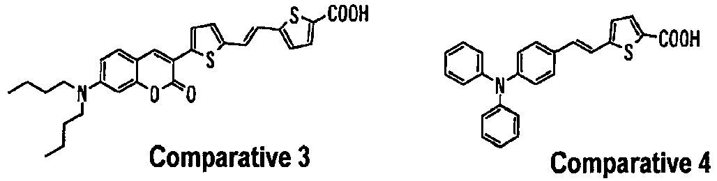
- The results of the resistance to removal in Table 3 (especially, comparisons of Example 1 and Comparative Example 1, Example 11 and Comparative Example 2, Example 4 and Comparative Example 3, Example 13 and Comparative Example 4, and Example 17 and Comparative Example 5) show that the compound of the invention represented by formula (1) has high adsorption durability. This shows that photoelectric conversion devices produced using the compound of the invention can stably and continuously maintain its photoelectric conversion efficiency.

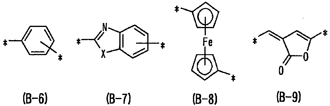

Claims (8)
- A novel compound represented by formula (1):
 A represents an optionally substituted aromatic hydrocarbon ring group or an optionally substituted aromatic heterocyclic group,B represents a group comprising a chain of one to four pieces of one or more groups selected from groups represented by formulae (B-1) to (B-13) below,R1, R2, and R3 each represent an optionally substituted hydrocarbon group or an optionally substituted hydrocarbonoxy group,at least one of R1, R2, and R3 represents an optionally substituted hydrocarbonoxy group,R4 and R5 each represent an optionally substituted hydrocarbon group,R4 and R5 may be linked together to form a ring, and R4 and R5 may be each independently linked with A to form a ring,

 X represents S, O, or NR, wherein R represents an optionally substituted hydrocarbon group, andany hydrogen atom may be replaced by a fluorine atom, a chlorine atom, a bromine atom, an iodine atom, a cyano group, a nitro group, a hydroxyl group, a thiol group, an -NR7R8 group, or an optionally substituted aliphatic hydrocarbon group, wherein R7 and R8 each represent an optionally substituted hydrocarbon group.
 - The novel compound according to claim 1, which satisfies at least one of the following conditions (i) to (iii):(i) the group represented by B has at least one piece of group represented by any one of formulae (B-1) to (B-9) and (B-11) to (B-13);(ii) R4 and R5 each represent an optionally substituted hydrocarbon group of 1 to 12 carbon atoms; and(iii) at least one of R4 and R5 is linked with A to form a ring.
- The novel compound according to claim 1 or 2, wherein R1, R2, and R3 in formula (1) each represent a linear or branched aliphatic hydrocarbonoxy group.
- The novel compound according to any one of claims 1 to 3, wherein partial structure (2) shown below in formula (1) is any one of partial structures (2-1) to (2-4) shown below.
 wherein A, R4, and R5 have the same meanings as in formula (1).
 wherein R4 and R5 have the same meanings as in formula (1).
 - The novel compound according to claim 4, wherein the partial structure (2) is the partial structure (2-1) or (2-2).
- The novel compound according to any one of claims 1 to 3, wherein partial structure (3) shown below in formula (1) is partial structure (3-1) or (3-2) shown below.
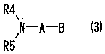 wherein A, B, R4, and R5 have the same meanings as in formula (1).
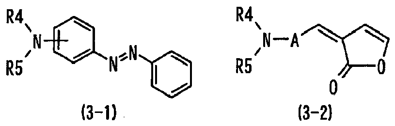 wherein A, R4, and R5 have the same meanings as in formula (1).
 - A support material comprising a support and the novel compound according to any one of claims 1 to 6 supported on the support.
- A photoelectric conversion device comprising an electrode having the support material according to claim 7.
Applications Claiming Priority (2)
| Application Number | Priority Date | Filing Date | Title |
|---|---|---|---|
| JP2011083421 | 2011-04-05 | ||
| PCT/JP2012/055755 WO2012137568A1 (en) | 2011-04-05 | 2012-03-07 | Novel compound and photoelectric conversion element |
Publications (2)
| Publication Number | Publication Date |
|---|---|
| EP2695886A1 true EP2695886A1 (en) | 2014-02-12 |
| EP2695886A4 EP2695886A4 (en) | 2014-12-03 |
Family
ID=46968972
Family Applications (1)
| Application Number | Title | Priority Date | Filing Date |
|---|---|---|---|
| EP12767952.0A Withdrawn EP2695886A4 (en) | 2011-04-05 | 2012-03-07 | NEW COMPOUND AND PHOTOELECTRIC CONVERSION ELEMENT |
Country Status (7)
| Country | Link |
|---|---|
| US (2) | US9324889B2 (en) |
| EP (1) | EP2695886A4 (en) |
| JP (1) | JP5914462B2 (en) |
| KR (1) | KR101874496B1 (en) |
| CN (1) | CN103415527B (en) |
| TW (1) | TW201243000A (en) |
| WO (1) | WO2012137568A1 (en) |
Families Citing this family (3)
| Publication number | Priority date | Publication date | Assignee | Title |
|---|---|---|---|---|
| CN103889990A (en) * | 2011-10-24 | 2014-06-25 | 株式会社艾迪科 | Dibenzo[b]furan compound, photoelectric conversion material and photoelectric conversion element |
| CN104051655A (en) * | 2013-03-11 | 2014-09-17 | 海洋王照明科技股份有限公司 | Inverted organic light emission diode device and manufacturing method thereof |
| KR102397160B1 (en) * | 2014-09-12 | 2022-05-11 | 스미또모 가가꾸 가부시끼가이샤 | Compound, and colored curable resin composition including said compound |
Family Cites Families (22)
| Publication number | Priority date | Publication date | Assignee | Title |
|---|---|---|---|---|
| JP2853902B2 (en) | 1993-02-03 | 1999-02-03 | 帝人株式会社 | Topical skin blood flow enhancer containing prostacyclin as active ingredient |
| DE69534293T2 (en) | 1994-12-21 | 2006-05-18 | Centre National De La Recherche Scientifique (C.N.R.S.) | Liquid, hydrophobic salts, their preparation and their use in electrochemistry |
| WO2002001667A1 (en) * | 2000-06-29 | 2002-01-03 | Nippon Kayaku Kabushiki Kaisha | Dye-sensitized photoelectric transducer |
| JP4095289B2 (en) | 2001-11-30 | 2008-06-04 | Tdk株式会社 | Dye-sensitized solar cell |
| JP4019139B2 (en) | 2002-05-13 | 2007-12-12 | 独立行政法人産業技術総合研究所 | Photoelectric conversion element using electrolyte solution containing 2-n-propylpyridine and dye-sensitized solar cell using the same |
| JP2005093313A (en) | 2003-09-19 | 2005-04-07 | Toyo Ink Mfg Co Ltd | An electrolyte composition for a dye-sensitized photoelectric conversion element, and a photoelectric conversion element using the same. |
| WO2006008951A1 (en) * | 2004-07-21 | 2006-01-26 | Sharp Kabushiki Kaisha | π-ELECTRON CONJUGATED ORGANOSILANE COMPOUND AND METHOD FOR SYNTHESIZING SAME |
| JP5086807B2 (en) * | 2005-05-13 | 2012-11-28 | Agcセイミケミカル株式会社 | Novel amino group-containing heterocyclic derivative and sensitizing dye for photoelectric conversion containing the heterocyclic derivative |
| JP4644818B2 (en) | 2006-09-05 | 2011-03-09 | 国立大学法人群馬大学 | Dye for dye-sensitized solar cell, photoelectric conversion element using the dye, and dye-sensitized solar cell |
| JP5280853B2 (en) * | 2006-11-07 | 2013-09-04 | Agcセイミケミカル株式会社 | Novel amino group-containing aromatic compound and sensitizing dye for photoelectric conversion containing the aromatic compound |
| JP2009269987A (en) * | 2008-05-07 | 2009-11-19 | Konica Minolta Business Technologies Inc | Novel compound, photoelectric transducer and solar cell |
| KR101115255B1 (en) * | 2008-07-11 | 2012-02-15 | 주식회사 엘지화학 | Novel anthracene derivatives and organic electronic devices using the same |
| JP2010027749A (en) | 2008-07-17 | 2010-02-04 | Mitsubishi Paper Mills Ltd | Material for photoelectric conversion element |
| KR20100066158A (en) * | 2008-12-09 | 2010-06-17 | 주식회사 동진쎄미켐 | Novel organic dye incorporating a trialkoxysilyl and preparation thereof |
| WO2010079051A1 (en) * | 2009-01-07 | 2010-07-15 | Basf Se | Silyl and heteroatom substituted compounds selected from carbazoles, dibenzofurans, dibenzothiophenes and dibenzo phospholes and the application thereof in organic electronics |
| WO2010125953A1 (en) | 2009-04-30 | 2010-11-04 | 横浜ゴム株式会社 | Electrolyte for photoelectric conversion element, photoelectric conversion element using the electrolyte, and dye-sensitized solar cell |
| KR20100130059A (en) * | 2009-06-02 | 2010-12-10 | 다우어드밴스드디스플레이머티리얼 유한회사 | Novel organic light emitting compound and organic light emitting device comprising the same |
| JP5401193B2 (en) | 2009-07-23 | 2014-01-29 | Tdk株式会社 | Dye for photoelectric conversion element and photoelectric conversion element |
| EP2781555A4 (en) * | 2011-11-18 | 2015-10-07 | Adeka Corp | NEW COMPOUND AND SUPPORT SUPPORTING THIS NEW COMPOUND |
| JP5874140B2 (en) * | 2011-12-28 | 2016-03-02 | 株式会社Adeka | Dye-sensitized solar cell |
| US20140178869A1 (en) | 2012-04-05 | 2014-06-26 | Advanced Cell Diagnostics, Inc. | Detection of immunoglobulin light chain restriction by rna in situ hybridization |
| JP6240172B2 (en) * | 2012-05-23 | 2017-11-29 | シーカ テクノロジー アクチェンゲゼルシャフト | Silane group-containing polymer |
-
2012
- 2012-03-07 KR KR1020137023833A patent/KR101874496B1/en not_active Expired - Fee Related
- 2012-03-07 JP JP2013508797A patent/JP5914462B2/en active Active
- 2012-03-07 EP EP12767952.0A patent/EP2695886A4/en not_active Withdrawn
- 2012-03-07 US US14/003,452 patent/US9324889B2/en not_active Expired - Fee Related
- 2012-03-07 WO PCT/JP2012/055755 patent/WO2012137568A1/en not_active Ceased
- 2012-03-07 CN CN201280012383.3A patent/CN103415527B/en not_active Expired - Fee Related
- 2012-03-15 TW TW101108936A patent/TW201243000A/en not_active IP Right Cessation
-
2016
- 2016-03-25 US US15/081,023 patent/US9812263B2/en not_active Expired - Fee Related
Also Published As
| Publication number | Publication date |
|---|---|
| JPWO2012137568A1 (en) | 2014-07-28 |
| US9324889B2 (en) | 2016-04-26 |
| TW201243000A (en) | 2012-11-01 |
| EP2695886A4 (en) | 2014-12-03 |
| WO2012137568A1 (en) | 2012-10-11 |
| JP5914462B2 (en) | 2016-05-11 |
| CN103415527B (en) | 2016-06-29 |
| US20130341572A1 (en) | 2013-12-26 |
| US20160211085A1 (en) | 2016-07-21 |
| TWI560246B (en) | 2016-12-01 |
| KR20140056159A (en) | 2014-05-09 |
| KR101874496B1 (en) | 2018-07-04 |
| US9812263B2 (en) | 2017-11-07 |
| CN103415527A (en) | 2013-11-27 |
Similar Documents
| Publication | Publication Date | Title |
|---|---|---|
| US9530571B2 (en) | Compound and support material supporting this novel compound | |
| CN104769045B (en) | Support body and photoelectric conversion element | |
| EP2800199B1 (en) | Dye-sensitized solar cell | |
| US9812263B2 (en) | Compound and photoelectric conversion device | |
| US9496095B2 (en) | Compound and carrier system having the compound | |
| WO2016108269A1 (en) | Compound, carrier, and photoelectric conversion element |
Legal Events
| Date | Code | Title | Description |
|---|---|---|---|
| PUAI | Public reference made under article 153(3) epc to a published international application that has entered the european phase |
Free format text: ORIGINAL CODE: 0009012 |
|
| 17P | Request for examination filed |
Effective date: 20130904 |
|
| AK | Designated contracting states |
Kind code of ref document: A1 Designated state(s): AL AT BE BG CH CY CZ DE DK EE ES FI FR GB GR HR HU IE IS IT LI LT LU LV MC MK MT NL NO PL PT RO RS SE SI SK SM TR |
|
| DAX | Request for extension of the european patent (deleted) | ||
| A4 | Supplementary search report drawn up and despatched |
Effective date: 20141104 |
|
| RIC1 | Information provided on ipc code assigned before grant |
Ipc: C07F 17/02 20060101ALN20141029BHEP Ipc: H01G 9/20 20060101ALI20141029BHEP Ipc: C07F 7/18 20060101AFI20141029BHEP |
|
| STAA | Information on the status of an ep patent application or granted ep patent |
Free format text: STATUS: EXAMINATION IS IN PROGRESS |
|
| 17Q | First examination report despatched |
Effective date: 20171117 |
|
| STAA | Information on the status of an ep patent application or granted ep patent |
Free format text: STATUS: THE APPLICATION HAS BEEN WITHDRAWN |
|
| 18W | Application withdrawn |
Effective date: 20181029 |