EP2690938A1 - Method for forming copper wiring, method for manufacturing wiring substrate, and wiring substrate - Google Patents
Method for forming copper wiring, method for manufacturing wiring substrate, and wiring substrate Download PDFInfo
- Publication number
- EP2690938A1 EP2690938A1 EP12761154.9A EP12761154A EP2690938A1 EP 2690938 A1 EP2690938 A1 EP 2690938A1 EP 12761154 A EP12761154 A EP 12761154A EP 2690938 A1 EP2690938 A1 EP 2690938A1
- Authority
- EP
- European Patent Office
- Prior art keywords
- suspension
- wiring
- copper
- copper particles
- wiring pattern
- Prior art date
- Legal status (The legal status is an assumption and is not a legal conclusion. Google has not performed a legal analysis and makes no representation as to the accuracy of the status listed.)
- Withdrawn
Links
Images


Classifications
-
- H—ELECTRICITY
- H05—ELECTRIC TECHNIQUES NOT OTHERWISE PROVIDED FOR
- H05K—PRINTED CIRCUITS; CASINGS OR CONSTRUCTIONAL DETAILS OF ELECTRIC APPARATUS; MANUFACTURE OF ASSEMBLAGES OF ELECTRICAL COMPONENTS
- H05K3/00—Apparatus or processes for manufacturing printed circuits
- H05K3/22—Secondary treatment of printed circuits
- H05K3/227—Drying of printed circuits
-
- H—ELECTRICITY
- H05—ELECTRIC TECHNIQUES NOT OTHERWISE PROVIDED FOR
- H05K—PRINTED CIRCUITS; CASINGS OR CONSTRUCTIONAL DETAILS OF ELECTRIC APPARATUS; MANUFACTURE OF ASSEMBLAGES OF ELECTRICAL COMPONENTS
- H05K3/00—Apparatus or processes for manufacturing printed circuits
- H05K3/10—Apparatus or processes for manufacturing printed circuits in which conductive material is applied to the insulating support in such a manner as to form the desired conductive pattern
- H05K3/12—Apparatus or processes for manufacturing printed circuits in which conductive material is applied to the insulating support in such a manner as to form the desired conductive pattern using thick film techniques, e.g. printing techniques to apply the conductive material or similar techniques for applying conductive paste or ink patterns
- H05K3/1283—After-treatment of the printed patterns, e.g. sintering or curing methods
-
- H—ELECTRICITY
- H05—ELECTRIC TECHNIQUES NOT OTHERWISE PROVIDED FOR
- H05K—PRINTED CIRCUITS; CASINGS OR CONSTRUCTIONAL DETAILS OF ELECTRIC APPARATUS; MANUFACTURE OF ASSEMBLAGES OF ELECTRICAL COMPONENTS
- H05K1/00—Printed circuits
- H05K1/02—Details
- H05K1/09—Use of materials for the conductive, e.g. metallic pattern
-
- H—ELECTRICITY
- H05—ELECTRIC TECHNIQUES NOT OTHERWISE PROVIDED FOR
- H05K—PRINTED CIRCUITS; CASINGS OR CONSTRUCTIONAL DETAILS OF ELECTRIC APPARATUS; MANUFACTURE OF ASSEMBLAGES OF ELECTRICAL COMPONENTS
- H05K3/00—Apparatus or processes for manufacturing printed circuits
- H05K3/22—Secondary treatment of printed circuits
- H05K3/24—Reinforcing of the conductive pattern
- H05K3/245—Reinforcing conductive patterns made by printing techniques or by other techniques for applying conductive pastes, inks or powders; Reinforcing other conductive patterns by such techniques
-
- H—ELECTRICITY
- H10—SEMICONDUCTOR DEVICES; ELECTRIC SOLID-STATE DEVICES NOT OTHERWISE PROVIDED FOR
- H10W—GENERIC PACKAGES, INTERCONNECTIONS, CONNECTORS OR OTHER CONSTRUCTIONAL DETAILS OF DEVICES COVERED BY CLASS H10
- H10W70/00—Package substrates; Interposers; Redistribution layers [RDL]
- H10W70/01—Manufacture or treatment
- H10W70/05—Manufacture or treatment of insulating or insulated package substrates, or of interposers, or of redistribution layers
- H10W70/098—Applying pastes or inks, e.g. screen printing
-
- H—ELECTRICITY
- H05—ELECTRIC TECHNIQUES NOT OTHERWISE PROVIDED FOR
- H05K—PRINTED CIRCUITS; CASINGS OR CONSTRUCTIONAL DETAILS OF ELECTRIC APPARATUS; MANUFACTURE OF ASSEMBLAGES OF ELECTRICAL COMPONENTS
- H05K1/00—Printed circuits
- H05K1/02—Details
- H05K1/09—Use of materials for the conductive, e.g. metallic pattern
- H05K1/092—Dispersed materials, e.g. conductive pastes or inks
- H05K1/097—Inks comprising nanoparticles and specially adapted for being sintered at low temperature
-
- H—ELECTRICITY
- H05—ELECTRIC TECHNIQUES NOT OTHERWISE PROVIDED FOR
- H05K—PRINTED CIRCUITS; CASINGS OR CONSTRUCTIONAL DETAILS OF ELECTRIC APPARATUS; MANUFACTURE OF ASSEMBLAGES OF ELECTRICAL COMPONENTS
- H05K2201/00—Indexing scheme relating to printed circuits covered by H05K1/00
- H05K2201/02—Fillers; Particles; Fibers; Reinforcement materials
- H05K2201/0203—Fillers and particles
- H05K2201/0263—Details about a collection of particles
- H05K2201/0266—Size distribution
-
- H—ELECTRICITY
- H05—ELECTRIC TECHNIQUES NOT OTHERWISE PROVIDED FOR
- H05K—PRINTED CIRCUITS; CASINGS OR CONSTRUCTIONAL DETAILS OF ELECTRIC APPARATUS; MANUFACTURE OF ASSEMBLAGES OF ELECTRICAL COMPONENTS
- H05K2203/00—Indexing scheme relating to apparatus or processes for manufacturing printed circuits covered by H05K3/00
- H05K2203/02—Details related to mechanical or acoustic processing, e.g. drilling, punching, cutting, using ultrasound
- H05K2203/0278—Flat pressure, e.g. for connecting terminals with anisotropic conductive adhesive
-
- H—ELECTRICITY
- H05—ELECTRIC TECHNIQUES NOT OTHERWISE PROVIDED FOR
- H05K—PRINTED CIRCUITS; CASINGS OR CONSTRUCTIONAL DETAILS OF ELECTRIC APPARATUS; MANUFACTURE OF ASSEMBLAGES OF ELECTRICAL COMPONENTS
- H05K2203/00—Indexing scheme relating to apparatus or processes for manufacturing printed circuits covered by H05K3/00
- H05K2203/14—Related to the order of processing steps
- H05K2203/1476—Same or similar kind of process performed in phases, e.g. coarse patterning followed by fine patterning
-
- H—ELECTRICITY
- H05—ELECTRIC TECHNIQUES NOT OTHERWISE PROVIDED FOR
- H05K—PRINTED CIRCUITS; CASINGS OR CONSTRUCTIONAL DETAILS OF ELECTRIC APPARATUS; MANUFACTURE OF ASSEMBLAGES OF ELECTRICAL COMPONENTS
- H05K3/00—Apparatus or processes for manufacturing printed circuits
- H05K3/10—Apparatus or processes for manufacturing printed circuits in which conductive material is applied to the insulating support in such a manner as to form the desired conductive pattern
- H05K3/12—Apparatus or processes for manufacturing printed circuits in which conductive material is applied to the insulating support in such a manner as to form the desired conductive pattern using thick film techniques, e.g. printing techniques to apply the conductive material or similar techniques for applying conductive paste or ink patterns
- H05K3/1241—Apparatus or processes for manufacturing printed circuits in which conductive material is applied to the insulating support in such a manner as to form the desired conductive pattern using thick film techniques, e.g. printing techniques to apply the conductive material or similar techniques for applying conductive paste or ink patterns by ink-jet printing or drawing by dispensing
- H05K3/125—Apparatus or processes for manufacturing printed circuits in which conductive material is applied to the insulating support in such a manner as to form the desired conductive pattern using thick film techniques, e.g. printing techniques to apply the conductive material or similar techniques for applying conductive paste or ink patterns by ink-jet printing or drawing by dispensing by ink-jet printing
-
- H—ELECTRICITY
- H10—SEMICONDUCTOR DEVICES; ELECTRIC SOLID-STATE DEVICES NOT OTHERWISE PROVIDED FOR
- H10W—GENERIC PACKAGES, INTERCONNECTIONS, CONNECTORS OR OTHER CONSTRUCTIONAL DETAILS OF DEVICES COVERED BY CLASS H10
- H10W20/00—Interconnections in chips, wafers or substrates
- H10W20/40—Interconnections external to wafers or substrates, e.g. back-end-of-line [BEOL] metallisations or vias connecting to gate electrodes
- H10W20/41—Interconnections external to wafers or substrates, e.g. back-end-of-line [BEOL] metallisations or vias connecting to gate electrodes characterised by their conductive parts
- H10W20/44—Conductive materials thereof
- H10W20/4473—Conductive organic materials, e.g. conductive adhesives or conductive inks
Definitions
- the present invention relates to a method of forming copper wiring, a method of manufacturing a wiring board, and a wiring board, and more particularly to a method of forming copper wiring, a method of manufacturing a wiring board, and a wiring board, in which copper wiring is formed with use of copper particles having different particle diameters.
- wiring boards which include insulating substrates and wiring patterns made of metal films formed on the surfaces of the insulating substrates, have widely been used for electronic components and semiconductor elements.
- the wiring pattern is formed by using a suspension with relatively large copper particles (e.g., having particle diameters of not smaller than 100 nm) dispersed therein, conductivity of the metal film declines due to deterioration over a period of time because there are large voids between the copper particles forming the metal film.
- relatively large copper particles e.g., having particle diameters of not smaller than 100 nm
- Patent Literature 1 describes a method of forming copper wiring by applying on a substrate a paste with copper particles having different particle diameters dispersed therein and calcining the paste.
- Patent Literature 2 describes a method of forming wiring by ejecting and depositing on a substrate two kinds of liquids which are respectively prepared by dispersing conductive fine particles in suspending media that are different from each other.
- Patent Literature 3 describes a method of forming wiring with a plurality of metallic thin films having different crystal grain sizes.
- the particles having the different particle diameters are mixed into one paste and are applied on the substrate, while in the method described in Patent Literature 2, the two kinds of liquids are used which are different in the properties of their suspending media but are identical in the properties of their conductive fine particles; and therefore, neither of the cases can sufficiently fill voids between the particles.
- the second metallic thin film having the crystal grain size smaller than the crystal grain size of the first metallic thin film is formed; however, no study has been made for filling the voids between the particles.
- the present invention has been contrived in view of these circumstances, an object thereof being to provide a method of forming copper wiring, a method of manufacturing a wiring board, and a wiring board, which are capable of improving conductivity and suppressing deterioration over a period of time by reducing voids between copper particles.
- a method of forming copper wiring includes: a wiring pattern formation step of depositing a first suspension onto a substrate to form a wiring pattern of the first suspension on the substrate, the first suspension including dispersed first copper particles having an average particle diameter that is not smaller than 100 nm; after the wiring pattern formation step, a drying step of drying the first copper particles in the wiring pattern at a temperature lower than 150°C; after the drying step, a second suspension deposition step of depositing a second suspension onto the wiring pattern, the second suspension including dispersed second copper particles having an average particle diameter that is smaller than the average particle diameter of the first copper particles; after the second suspension deposition step, a compaction step of reducing voids between the first and second copper particles in the wiring pattern; after the compaction step, a heat application step of applying heat to the first and second copper particles in the wiring pattern; and after the heat application step, a reducing treatment step of subjecting the first and second copper particles in the wiring pattern to a
- the second copper particles into voids between the first copper particles in the wiring pattern, by forming the wiring pattern with the first copper particles having the average particle diameter that is not smaller than 100 nm and thereafter depositing the second copper particles having the average particle diameter that is smaller than the average particle diameter of the first copper particles onto the wiring pattern.
- it is possible to improve temporal stability of the copper wiring because the voids between the copper particles forming the wiring pattern can be reduced.
- the compaction step includes a pressure application step of applying pressure to the first and second copper particles in the wiring pattern.
- the wiring pattern formation step includes a first suspension ejection step of ejecting droplets of the first suspension by means of an inkjet method to deposit the droplets of the first suspension onto the substrate; and the second suspension deposition step includes a second suspension ejection step of ejecting droplets of the second suspension by means of the inkjet method to deposit the droplets of the second suspension onto the wiring pattern.
- the inkjet method in the wiring pattern formation step and in the second suspension deposition step, it is possible to easily perform the steps. Moreover, it is possible to selectively deposit the first and second suspensions only to a portion on the substrate which is necessary for the formation of the wiring pattern, and it is possible to thereby suppress use amounts of the first and second suspensions and to thus lower a manufacturing cost of the copper wiring.
- a size of the droplets of the first suspension in the first suspension ejection step is larger than a size of the droplets of the second suspension in the second suspension ejection step.
- the first suspension ejection step and the second suspension ejection step are carried out respectively by means of inkjet heads different from each other.
- the average particle diameter of the second copper particles is not larger than 1/10 of the average particle diameter of the first copper particles.
- a viscosity of the second suspension is lower than a viscosity of the first suspension.
- a method of manufacturing a wiring board according to one aspect of the present invention includes the above-described method of forming copper wiring.
- the method of manufacturing the wiring board is adequate since it is possible to form the copper wiring with improved conductivity and temporal stability.
- a wiring board according to one aspect of the present invention includes the copper wiring formed by the above-described method of forming copper wiring.
- the wiring board can include the copper wiring with improved conductivity and temporal stability.
- copper particles having a relatively small particle diameter are inserted into voids between copper particles having a relatively large particle diameter, then the voids are further reduced by a compaction treatment, and thereafter the copper particles are made to oxidize and bond to each other by applying heat; therefore, it is possible to increase mutual contact areas between the copper particles and to thereby improve conductivity and suppress deterioration over a period of time of copper wiring.
- a first suspension 12 in which a plurality of first copper particles 14 (first copper powder) are dispersed is deposited onto a substrate 10 to form a wiring pattern of the first suspension 12 on the substrate 10 (see Fig. 1A ).
- a width of the wiring pattern is preferably not smaller than 50 ⁇ m and not larger than 100 ⁇ m, without particular limitations.
- substrates of various materials can be used without particular limitations.
- the first suspension 12 includes a suspending medium (continuous phase) and the plurality of first copper particles 14 (the first copper powder) dispersed within the suspending medium.
- the first suspension 12 can include a dispersing agent that is capable of holding the first copper particles 14 in the dispersed state in the suspending medium.
- the first suspension 12 can further include any additive agent that is evaporated or broken at a temperature not higher than a heating temperature in a heat application step, which is described later. In Fig. 1A , only the first copper particles 14 are particularly depicted among the contents of the first suspension 12.
- the first copper powder is constituted of the first copper particles 14 having a number-average particle diameter measured by scanning electron microscopy (SEM) (hereinafter referred to simply as the "particle diameter") that is not smaller than 100 nm and not larger than 300 nm.
- SEM scanning electron microscopy
- the copper particles do not completely oxidize easily in the air at the normal temperature.
- the copper particles in a case where the copper particles have the particle diameter that is smaller than 100 nm, the copper particles completely oxidize easily in the air at the normal temperature.
- the suspending medium it is possible to use any of various liquids (e.g., cyclohexanone, or the like) without particular limitations, provided that the first copper particles 14 can be dispersed therein.
- various liquids e.g., cyclohexanone, or the like
- the dispersing agent it is possible to use any of various materials without particular limitations, provided that the material is capable of holding the first copper particles 14 in the dispersed state in the suspending medium.
- the dispersing agent is made of the material preferably providing the first copper particles 14 with sufficient dispersion stability, and preferably not involving in the conductivity of completed copper wiring.
- the first suspension 12 is prepared in a non-oxidizing atmosphere.
- the first copper particles 14 do not easily oxidize in the air at the normal temperature because the first copper powder constituted of the first copper particles 14 having the particle diameter that is not smaller than 100 nm is used in the present embodiment, the preparation of the first suspension 12 in the non-oxidizing atmosphere is useful for preventing the first copper powder from oxidizing.
- the first suspension 12 has the viscosity that is not lower than 1 cP and not higher than 20 cP and the surface tension that is not lower than 25 mN/m and not higher than 40 mN/m.
- the first suspension 12 by mixing the first copper particles of 50 wt% or above and cyclohexanone of 50 wt% or less, for example.
- the method of depositing the first suspension 12 onto the substrate 10 it is possible to use any of various coating methods such as a spin coating method and a dip coating method, or any of various printing methods such as an inkjet printing method and a screen printing method, without particular limitations.
- a desired wiring pattern can directly be drawn on the substrate 10 with the first suspension 12.
- the inkjet printing method it is possible to selectively deposit the first suspension 12 along a wiring pattern, and it is possible to thereby suppress a use amount of the first suspension 12 and to thus lower a manufacturing cost of copper wiring.
- the suspending medium is removed from the first suspension 12 that has been deposited on the substrate 10 in the pattern formation step, so that the first copper powder is dried (see Fig. 1B ). Thereby, it is possible to facilitate insertion of the second suspension 16 into the voids between the first copper particles 14 in the subsequent second suspension deposition step.
- the temperature at which the first copper powder is dried in the first drying step is lower than 150°C. It is more preferable that the first copper powder is not heated in the first drying step. By limiting the temperature in the first drying step as described above, it is possible to prevent the first copper powder from oxidizing.
- the first drying step it is possible to accelerate the drying of the first copper powder by blowing air and/or lowering the atmospheric pressure.
- the second suspension 16 in which the plurality of second copper particles 18 (second copper powder) are dispersed, is deposited onto the wiring pattern formed of the first copper powder that has been dried in the first drying step (see Fig. 1C ).
- the second suspension 16 includes a suspending medium (continuous phase) and the plurality of second copper particles 18 (the second copper powder) dispersed within the suspending medium.
- the second suspension 16 can include a dispersing agent that is capable of holding the second copper particles 18 in the dispersed state in the suspending medium.
- the second suspension 16 can further include any additive agent that is evaporated or broken at a temperature not higher than the heating temperature in the heat application step, which is described later. In Fig. 1C , only the second copper particles 18 are particularly depicted among the contents of the second suspension 16.
- the second copper particles 18 constituting the second copper powder have a particle diameter smaller than the particle diameter of the first copper particles 14. Hence, it is possible to insert the second copper particles 18 into the voids between the first copper particles 14 and to thereby reduce the voids.
- the particle diameter of the second copper particles 18 is preferably not larger than 30 nm, and is more preferably not larger than 1/10 of the particle diameter of the first copper particles 14. Hence, the second copper particles 18 can easily enter into the voids between the first copper particles 14. On the other hand, in a case where the particle diameter of the second copper particles 18 is small, the second copper particles 18 easily oxidize in the second suspension deposition step. Therefore, it is preferable that the second copper particles 18 have the particle diameter that prevents easy oxidation at the normal temperature, and have the particle diameter that is not smaller than 10 nm, for example.
- the suspending medium As the suspending medium, the dispersing agent and other contents included in the second suspension 16, it is possible to use the materials similar to the first dispersion liquid 12. It is preferable that the second suspension 16 is prepared in a non-oxidizing atmosphere.
- the second suspension 16 by mixing the second copper particles of 25 wt% or above and cyclohexanone of 75 wt% or less, for example.
- the viscosity of the second suspension 16 is not lower than 1 cP and not higher than 20 cP, and is lower than the viscosity of the first suspension 12. Hence, the second suspension 16 can easily enter into the voids between the first copper particles 14. It is preferable that the surface tension of the second suspension 16 is not lower than 25 mN/m and not higher than 40 mN/m.
- the inkjet printing method is used to deposit the second suspension 16
- the first suspension 12 and the second suspension 16 are ejected from different inkjet heads, respectively.
- the first and second copper powders are respectively deposited with use of the first and second suspensions, it is possible to improve electivity of properties in the deposition by the inkjet printing method as compared with a case where copper powder constituted of copper particles different in particle diameters is deposited with use of the same suspension.
- the size of droplets of the second suspension 16 ejected by the inkjet is smaller than the size of droplets of the first suspension 12 ejected by the inkjet. Hence, the second suspension 16 can easily enter into the voids between the first copper particles 14.
- the second drying step is performed after elapse of a time that is long enough to complete entrance of the second copper particles 18 into the voids between the first copper particles 14.
- the suspending medium of the second suspension 16 is left to maintain flowability of the second suspension 16, which makes it possible to keep the state where the second copper particles 18 can easily enter into the voids between the first copper particles 14. It is also possible to reduce process time.
- the compaction step can be performed in the state where the voids are smaller than those in a case where the second copper particles 18 are not deposited. Therefore, it becomes possible to make the pressure applied for the compaction relatively low, and to thereby suppress an adverse effect on the substrate 10.
- Examples of the pressure application method in the compaction step include a calendering process. It is preferable that the pressure applied to the copper powder in the compaction step is not lower than 100 MPa and not higher than 300 MPa.
- the heating temperature in the heat application step it is preferable to determine the heating temperature in the heat application step according to the particle diameter of the first copper particles 14 constituting the first copper powder.
- the heating temperature in the heat application step is not lower than 150°C.
- conductivity can be imparted to the wiring pattern if the heating temperature in the heat application step is not lower than 200°C.
- the heat application step after the compaction step. After reducing the voids between the copper particles forming the wiring pattern, it is possible to further increase mutual contact areas between the copper particles by making the copper particles oxidize and bond to each other with the heat application. If the order of performing the compaction step and the heat application step is reversed (i.e., the compaction step is performed after the heat application step), the compaction step is performed on the copper powder in the state where the copper particles have already bonded to each other by heat in the heat application step, and this makes it difficult to reduce the voids between the copper particles to compact the copper powder.
- the compaction step and the heat application step are simultaneously performed on the copper powder, the copper particles bond to each other in the state where the copper powder is not sufficiently compacted, and it is then impossible to secure sufficient mutual contact areas between the copper particles. It is preferable, therefore, to perform the compaction step first and to thereafter perform the heat application step.
- the copper powder having oxidized in the heat application step is reduced so as to impart conductivity to the copper powder forming the wiring pattern (see Fig. 1F ).
- the first copper particles 14 and the second copper particles 18, which have bonded to each other, function as wiring.
- the reducing treatment it is possible to use any of various treatments without particular limitations.
- the width of the copper wiring formed in the present embodiment is, for example, not smaller than 50 ⁇ m and not larger than 100 ⁇ m, without particular limitations.
- the copper wiring formed in the present embodiment can be used as wiring for wiring boards.
- the wiring pattern in the wiring pattern formation step, is formed with use of the first copper particles having the large particle diameter, and in the subsequent second suspension deposition step, the second copper particles having the particle diameter smaller than the particle diameter of the first copper particles are deposited onto the wiring pattern to fill the voids between the first copper particles with the second copper particles, so that the copper wiring with small voids can be formed. Therefore, it is possible to improve conductivity as well as temporal stability in the completed copper wiring.
- Fig. 2A shows a first comparative example, where second copper particles 118 having a small particle diameter are deposited on a substrate 10 first, and thereafter first copper particles 114 having a large particle diameter are deposited.
- a layer of the first copper particles 114 is merely formed on a layer of the second copper particles 118, and it is not possible to obtain any effect of the second copper particles 118 filling voids between the first copper particles 114.
- Fig. 2B shows a second comparative example, where a suspension is prepared in which both first copper particles 214 having a large particle diameter and second copper particles 218 having a small particle diameter are dispersed, and the suspension is deposited on a substrate 10.
- some of the second copper particles 218 enter into voids between the first copper particles 214.
- some of the second copper particles 218 remain on the first copper particles 214, and are then wasted with producing no effect of filling the voids between the first copper particles 214.
Landscapes
- Engineering & Computer Science (AREA)
- Microelectronics & Electronic Packaging (AREA)
- Manufacturing & Machinery (AREA)
- Manufacturing Of Printed Wiring (AREA)
- Internal Circuitry In Semiconductor Integrated Circuit Devices (AREA)
- Manufacturing Of Electric Cables (AREA)
- Electrodes Of Semiconductors (AREA)
Abstract
Description
- The present invention relates to a method of forming copper wiring, a method of manufacturing a wiring board, and a wiring board, and more particularly to a method of forming copper wiring, a method of manufacturing a wiring board, and a wiring board, in which copper wiring is formed with use of copper particles having different particle diameters.
- Conventionally, wiring boards which include insulating substrates and wiring patterns made of metal films formed on the surfaces of the insulating substrates, have widely been used for electronic components and semiconductor elements.
- In a case where the wiring pattern is formed by using a suspension with relatively large copper particles (e.g., having particle diameters of not smaller than 100 nm) dispersed therein, conductivity of the metal film declines due to deterioration over a period of time because there are large voids between the copper particles forming the metal film.
- In a case where copper nanoparticles (e.g., having particle diameters of smaller than 100 nm) are used for improving denseness of the metal film, the copper nanoparticles completely oxidize easily in the air in the process of forming the wiring pattern, it is then impossible to make the particles bond together even with a reducing treatment performed thereafter, and the conductivity of the wiring pattern cannot be realized. Moreover, since costs of particles having small particle diameters are high, a manufacturing cost of wiring boards is increased.
- For example, Patent Literature 1 describes a method of forming copper wiring by applying on a substrate a paste with copper particles having different particle diameters dispersed therein and calcining the paste. Patent Literature 2 describes a method of forming wiring by ejecting and depositing on a substrate two kinds of liquids which are respectively prepared by dispersing conductive fine particles in suspending media that are different from each other. Patent Literature 3 describes a method of forming wiring with a plurality of metallic thin films having different crystal grain sizes.
-
- Patent Literature 1: Japanese Patent Application Publication No.
10-308120 - Patent Literature 2: Japanese Patent Application Publication No.
2003-311196 - Patent Literature 3: Japanese Patent Application Publication No.
05-013412 - In the method described in Patent Literature 1, the particles having the different particle diameters are mixed into one paste and are applied on the substrate, while in the method described in Patent Literature 2, the two kinds of liquids are used which are different in the properties of their suspending media but are identical in the properties of their conductive fine particles; and therefore, neither of the cases can sufficiently fill voids between the particles. In the method described in Patent Literature 3, over the first metallic thin film, the second metallic thin film having the crystal grain size smaller than the crystal grain size of the first metallic thin film is formed; however, no study has been made for filling the voids between the particles.
- The present invention has been contrived in view of these circumstances, an object thereof being to provide a method of forming copper wiring, a method of manufacturing a wiring board, and a wiring board, which are capable of improving conductivity and suppressing deterioration over a period of time by reducing voids between copper particles.
- In order to attain the aforementioned object, a method of forming copper wiring according to one aspect of the present invention includes: a wiring pattern formation step of depositing a first suspension onto a substrate to form a wiring pattern of the first suspension on the substrate, the first suspension including dispersed first copper particles having an average particle diameter that is not smaller than 100 nm; after the wiring pattern formation step, a drying step of drying the first copper particles in the wiring pattern at a temperature lower than 150°C; after the drying step, a second suspension deposition step of depositing a second suspension onto the wiring pattern, the second suspension including dispersed second copper particles having an average particle diameter that is smaller than the average particle diameter of the first copper particles; after the second suspension deposition step, a compaction step of reducing voids between the first and second copper particles in the wiring pattern; after the compaction step, a heat application step of applying heat to the first and second copper particles in the wiring pattern; and after the heat application step, a reducing treatment step of subjecting the first and second copper particles in the wiring pattern to a reducing treatment.
- According to this aspect, it is possible to insert the second copper particles into voids between the first copper particles in the wiring pattern, by forming the wiring pattern with the first copper particles having the average particle diameter that is not smaller than 100 nm and thereafter depositing the second copper particles having the average particle diameter that is smaller than the average particle diameter of the first copper particles onto the wiring pattern. Thus, it is possible to reduce the voids present between the copper particles at the time of forming the wiring pattern. Moreover, it is possible to increase mutual contact areas between the copper particles and to thereby improve the conductivity of the copper wiring, by reducing the voids between the copper particles with the compaction treatment, and thereafter making the copper particles oxidize and bond to each other with the heat application. Further, it is possible to improve temporal stability of the copper wiring because the voids between the copper particles forming the wiring pattern can be reduced.
- Preferably, the compaction step includes a pressure application step of applying pressure to the first and second copper particles in the wiring pattern.
- According to this aspect, it is possible to perform the compaction treatment to reduce the voids between the copper particles by applying pressure to the first and second copper particles in the wiring pattern.
- Preferably, the wiring pattern formation step includes a first suspension ejection step of ejecting droplets of the first suspension by means of an inkjet method to deposit the droplets of the first suspension onto the substrate; and the second suspension deposition step includes a second suspension ejection step of ejecting droplets of the second suspension by means of the inkjet method to deposit the droplets of the second suspension onto the wiring pattern.
- According to this aspect, by using the inkjet method in the wiring pattern formation step and in the second suspension deposition step, it is possible to easily perform the steps. Moreover, it is possible to selectively deposit the first and second suspensions only to a portion on the substrate which is necessary for the formation of the wiring pattern, and it is possible to thereby suppress use amounts of the first and second suspensions and to thus lower a manufacturing cost of the copper wiring.
- Preferably, a size of the droplets of the first suspension in the first suspension ejection step is larger than a size of the droplets of the second suspension in the second suspension ejection step.
- According to this aspect, it becomes easy to insert the second suspension into the voids between the first copper particles.
- Preferably, the first suspension ejection step and the second suspension ejection step are carried out respectively by means of inkjet heads different from each other.
- According to this aspect, it is possible to efficiently perform the ejections of the first and second suspensions.
- Preferably, the average particle diameter of the second copper particles is not larger than 1/10 of the average particle diameter of the first copper particles.
- According to this aspect, it becomes easy to insert the second copper particles into the voids between the first copper particles.
- Preferably, a viscosity of the second suspension is lower than a viscosity of the first suspension.
- According to this aspect, it becomes easy to insert the second suspension into the voids between the first copper particles.
- Moreover, in order to attain the aforementioned object, a method of manufacturing a wiring board according to one aspect of the present invention includes the above-described method of forming copper wiring.
- According to this aspect, the method of manufacturing the wiring board is adequate since it is possible to form the copper wiring with improved conductivity and temporal stability.
- Furthermore, in order to attain the aforementioned object, a wiring board according to one aspect of the present invention includes the copper wiring formed by the above-described method of forming copper wiring.
- According to this aspect, the wiring board can include the copper wiring with improved conductivity and temporal stability.
- According to the present invention, copper particles having a relatively small particle diameter are inserted into voids between copper particles having a relatively large particle diameter, then the voids are further reduced by a compaction treatment, and thereafter the copper particles are made to oxidize and bond to each other by applying heat; therefore, it is possible to increase mutual contact areas between the copper particles and to thereby improve conductivity and suppress deterioration over a period of time of copper wiring.
-
- [
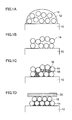
Fig. 1A ] A view for explaining a method of forming copper wiring according to an embodiment of the present invention. - [
Fig. 1B ] A view for explaining the method of forming copper wiring according to the embodiment of the present invention. - [
Fig. 1C ] A view for explaining the method of forming copper wiring according to the embodiment of the present invention. - [
Fig. 1D ] A view for explaining the method of forming copper wiring according to the embodiment of the present invention. - [
Fig. 1E ] A view for explaining the method of forming copper wiring according to the embodiment of the present invention. - [
Fig. 1F ] A view for explaining the method of forming copper wiring according to the embodiment of the present invention. - [
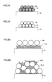
Fig. 2A ] A view for explaining a method of forming copper wiring according to a comparative example. - [
Fig. 2B ] A view for explaining a method of forming copper wiring according to a comparative example. - Hereinafter, preferred embodiments of the present invention are described with reference to the accompanying drawings.
- In a method of forming copper wiring according to an embodiment of the present invention, firstly, a
first suspension 12 in which a plurality of first copper particles 14 (first copper powder) are dispersed is deposited onto asubstrate 10 to form a wiring pattern of thefirst suspension 12 on the substrate 10 (seeFig. 1A ). A width of the wiring pattern is preferably not smaller than 50 µm and not larger than 100 µm, without particular limitations. - <Substrate>
- As the
substrate 10, substrates of various materials can be used without particular limitations. - The
first suspension 12 includes a suspending medium (continuous phase) and the plurality of first copper particles 14 (the first copper powder) dispersed within the suspending medium. Thefirst suspension 12 can include a dispersing agent that is capable of holding thefirst copper particles 14 in the dispersed state in the suspending medium. Thefirst suspension 12 can further include any additive agent that is evaporated or broken at a temperature not higher than a heating temperature in a heat application step, which is described later. InFig. 1A , only thefirst copper particles 14 are particularly depicted among the contents of thefirst suspension 12. - It is preferable that the first copper powder is constituted of the
first copper particles 14 having a number-average particle diameter measured by scanning electron microscopy (SEM) (hereinafter referred to simply as the "particle diameter") that is not smaller than 100 nm and not larger than 300 nm. In the case where the copper particles have the particle diameter that is not smaller than 100 nm, the copper particles do not completely oxidize easily in the air at the normal temperature. On the other hand, in a case where the copper particles have the particle diameter that is smaller than 100 nm, the copper particles completely oxidize easily in the air at the normal temperature. - As the suspending medium, it is possible to use any of various liquids (e.g., cyclohexanone, or the like) without particular limitations, provided that the
first copper particles 14 can be dispersed therein. - As the dispersing agent, it is possible to use any of various materials without particular limitations, provided that the material is capable of holding the
first copper particles 14 in the dispersed state in the suspending medium. The dispersing agent is made of the material preferably providing thefirst copper particles 14 with sufficient dispersion stability, and preferably not involving in the conductivity of completed copper wiring. - It is preferable that the
first suspension 12 is prepared in a non-oxidizing atmosphere. Although thefirst copper particles 14 do not easily oxidize in the air at the normal temperature because the first copper powder constituted of thefirst copper particles 14 having the particle diameter that is not smaller than 100 nm is used in the present embodiment, the preparation of thefirst suspension 12 in the non-oxidizing atmosphere is useful for preventing the first copper powder from oxidizing. - It is preferable that the
first suspension 12 has the viscosity that is not lower than 1 cP and not higher than 20 cP and the surface tension that is not lower than 25 mN/m and not higher than 40 mN/m. By thus adjusting the property of thefirst suspension 12, it is possible to facilitate insertion ofsecond copper particles 18 into voids between thefirst copper particles 14 when depositing asecond suspension 16, which is described later. - It is possible to prepare the
first suspension 12 by mixing the first copper particles of 50 wt% or above and cyclohexanone of 50 wt% or less, for example. - As the method of depositing the
first suspension 12 onto thesubstrate 10, it is possible to use any of various coating methods such as a spin coating method and a dip coating method, or any of various printing methods such as an inkjet printing method and a screen printing method, without particular limitations. In a case where the inkjet printing method is used among these methods, a desired wiring pattern can directly be drawn on thesubstrate 10 with thefirst suspension 12. Moreover, in the case where the inkjet printing method is used, it is possible to selectively deposit thefirst suspension 12 along a wiring pattern, and it is possible to thereby suppress a use amount of thefirst suspension 12 and to thus lower a manufacturing cost of copper wiring. - Next, the suspending medium is removed from the
first suspension 12 that has been deposited on thesubstrate 10 in the pattern formation step, so that the first copper powder is dried (seeFig. 1B ). Thereby, it is possible to facilitate insertion of thesecond suspension 16 into the voids between thefirst copper particles 14 in the subsequent second suspension deposition step. - It is preferable that the temperature at which the first copper powder is dried in the first drying step is lower than 150°C. It is more preferable that the first copper powder is not heated in the first drying step. By limiting the temperature in the first drying step as described above, it is possible to prevent the first copper powder from oxidizing.
- In the first drying step, it is possible to accelerate the drying of the first copper powder by blowing air and/or lowering the atmospheric pressure.
- Next, the
second suspension 16, in which the plurality of second copper particles 18 (second copper powder) are dispersed, is deposited onto the wiring pattern formed of the first copper powder that has been dried in the first drying step (seeFig. 1C ). - The
second suspension 16 includes a suspending medium (continuous phase) and the plurality of second copper particles 18 (the second copper powder) dispersed within the suspending medium. Thesecond suspension 16 can include a dispersing agent that is capable of holding thesecond copper particles 18 in the dispersed state in the suspending medium. Thesecond suspension 16 can further include any additive agent that is evaporated or broken at a temperature not higher than the heating temperature in the heat application step, which is described later. InFig. 1C , only thesecond copper particles 18 are particularly depicted among the contents of thesecond suspension 16. - The
second copper particles 18 constituting the second copper powder have a particle diameter smaller than the particle diameter of thefirst copper particles 14. Hence, it is possible to insert thesecond copper particles 18 into the voids between thefirst copper particles 14 and to thereby reduce the voids. - The particle diameter of the
second copper particles 18 is preferably not larger than 30 nm, and is more preferably not larger than 1/10 of the particle diameter of thefirst copper particles 14. Hence, thesecond copper particles 18 can easily enter into the voids between thefirst copper particles 14. On the other hand, in a case where the particle diameter of thesecond copper particles 18 is small, thesecond copper particles 18 easily oxidize in the second suspension deposition step. Therefore, it is preferable that thesecond copper particles 18 have the particle diameter that prevents easy oxidation at the normal temperature, and have the particle diameter that is not smaller than 10 nm, for example. - As the suspending medium, the dispersing agent and other contents included in the
second suspension 16, it is possible to use the materials similar to thefirst dispersion liquid 12. It is preferable that thesecond suspension 16 is prepared in a non-oxidizing atmosphere. - It is possible to prepare the
second suspension 16 by mixing the second copper particles of 25 wt% or above and cyclohexanone of 75 wt% or less, for example. - It is preferable that the viscosity of the
second suspension 16 is not lower than 1 cP and not higher than 20 cP, and is lower than the viscosity of thefirst suspension 12. Hence, thesecond suspension 16 can easily enter into the voids between thefirst copper particles 14. It is preferable that the surface tension of thesecond suspension 16 is not lower than 25 mN/m and not higher than 40 mN/m. - As the method of depositing the
second suspension 16 onto the wiring pattern, it is possible to use the method similar to the method of depositing thefirst suspension 12, without particular limitations. - In a case where the inkjet printing method is used to deposit the
second suspension 16, it is possible to selectively deposit thesecond suspension 16 along the wiring pattern, and it is possible to thereby suppress a use amount of thesecond suspension 16 and to thus lower the manufacturing cost of the copper wiring. In this case, it is preferable that the size of droplets of thesecond suspension 16 ejected by the inkjet is smaller than the width of the wiring pattern. - In the case where the inkjet printing method is used to deposit the
first suspension 12 and thesecond suspension 16, it is preferable that thefirst suspension 12 and thesecond suspension 16 are ejected from different inkjet heads, respectively. In the present embodiment, since the first and second copper powders are respectively deposited with use of the first and second suspensions, it is possible to improve electivity of properties in the deposition by the inkjet printing method as compared with a case where copper powder constituted of copper particles different in particle diameters is deposited with use of the same suspension. It is preferable that the size of droplets of thesecond suspension 16 ejected by the inkjet is smaller than the size of droplets of thefirst suspension 12 ejected by the inkjet. Hence, thesecond suspension 16 can easily enter into the voids between thefirst copper particles 14. - It is possible to perform, where necessary, a second drying step in which the suspending medium is removed from the
second suspension 16 that has been deposited on the wiring pattern, so that the copper powder is dried. In this case, it is preferable that the second drying step is performed after elapse of a time that is long enough to complete entrance of thesecond copper particles 18 into the voids between thefirst copper particles 14. - It is also possible not to perform the second drying step. In this case, the suspending medium of the
second suspension 16 is left to maintain flowability of thesecond suspension 16, which makes it possible to keep the state where thesecond copper particles 18 can easily enter into the voids between thefirst copper particles 14. It is also possible to reduce process time. - Next, the voids between the
first copper particles 14 and thesecond copper particles 18 are reduced, so that the copper powder forming the wiring pattern is compacted (seeFig. 1D ). - For example, it is possible to compress and thereby compact the copper powder by applying pressure with a
pressing device 20 as shown inFig. 1D . In the present embodiment, since thesecond copper particles 18 have been inserted in the voids between thefirst copper particles 14 in the second suspension deposition step, the compaction step can be performed in the state where the voids are smaller than those in a case where thesecond copper particles 18 are not deposited. Therefore, it becomes possible to make the pressure applied for the compaction relatively low, and to thereby suppress an adverse effect on thesubstrate 10. - By performing the compaction step, it becomes possible to suppress a deposition amount of the
second copper particles 18, and to thereby lower the manufacturing cost of the copper wiring. - Examples of the pressure application method in the compaction step include a calendering process. It is preferable that the pressure applied to the copper powder in the compaction step is not lower than 100 MPa and not higher than 300 MPa.
- Next, heat is applied in the air to the copper powder that has been compacted in the compaction step, so as to make the
first copper particles 14 and thesecond copper particles 18 bond to each other concurrently with oxidizing (seeFig. 1E ). - It is preferable to determine the heating temperature in the heat application step according to the particle diameter of the
first copper particles 14 constituting the first copper powder. In order to impart conductivity to the wiring pattern, it is preferable to heat, in the heat application step, the copper powder at a higher temperature as the particle diameter of the copper particles constituting the copper powder becomes larger. For example, in a case where thefirst copper particles 14 constituting the first copper powder have the particle diameter that is not smaller than 100 nm and not larger than 200 nm, conductivity can be imparted to the wiring pattern if the heating temperature in the heat application step is not lower than 150°C. For example, in a case where thefirst copper particles 14 constituting the first copper powder have the particle diameter that is larger than 200 nm, conductivity can be imparted to the wiring pattern if the heating temperature in the heat application step is not lower than 200°C. - In the present embodiment, it is preferable to perform the heat application step after the compaction step. After reducing the voids between the copper particles forming the wiring pattern, it is possible to further increase mutual contact areas between the copper particles by making the copper particles oxidize and bond to each other with the heat application. If the order of performing the compaction step and the heat application step is reversed (i.e., the compaction step is performed after the heat application step), the compaction step is performed on the copper powder in the state where the copper particles have already bonded to each other by heat in the heat application step, and this makes it difficult to reduce the voids between the copper particles to compact the copper powder. If the compaction step and the heat application step are simultaneously performed on the copper powder, the copper particles bond to each other in the state where the copper powder is not sufficiently compacted, and it is then impossible to secure sufficient mutual contact areas between the copper particles. It is preferable, therefore, to perform the compaction step first and to thereafter perform the heat application step.
- Next, the copper powder having oxidized in the heat application step is reduced so as to impart conductivity to the copper powder forming the wiring pattern (see
Fig. 1F ). Thereby, it is possible to make thefirst copper particles 14 and thesecond copper particles 18, which have bonded to each other, function as wiring. - As the reducing treatment, it is possible to use any of various treatments without particular limitations. For example, it is possible to reduce the oxidized copper powder by heating at a temperature of not lower than 350°C and not higher than 400°C in an argon atmosphere containing hydrogen of not less than 3 vol% and not more than 10 vol%.
- The width of the copper wiring formed in the present embodiment is, for example, not smaller than 50 µm and not larger than 100 µm, without particular limitations. The copper wiring formed in the present embodiment can be used as wiring for wiring boards.
- According to the present embodiment, in the wiring pattern formation step, the wiring pattern is formed with use of the first copper particles having the large particle diameter, and in the subsequent second suspension deposition step, the second copper particles having the particle diameter smaller than the particle diameter of the first copper particles are deposited onto the wiring pattern to fill the voids between the first copper particles with the second copper particles, so that the copper wiring with small voids can be formed. Therefore, it is possible to improve conductivity as well as temporal stability in the completed copper wiring.
-
Fig. 2A shows a first comparative example, wheresecond copper particles 118 having a small particle diameter are deposited on asubstrate 10 first, and thereafterfirst copper particles 114 having a large particle diameter are deposited. In this case, a layer of thefirst copper particles 114 is merely formed on a layer of thesecond copper particles 118, and it is not possible to obtain any effect of thesecond copper particles 118 filling voids between thefirst copper particles 114. -
Fig. 2B shows a second comparative example, where a suspension is prepared in which bothfirst copper particles 214 having a large particle diameter andsecond copper particles 218 having a small particle diameter are dispersed, and the suspension is deposited on asubstrate 10. In this case, some of thesecond copper particles 218 enter into voids between thefirst copper particles 214. However, some of thesecond copper particles 218 remain on thefirst copper particles 214, and are then wasted with producing no effect of filling the voids between thefirst copper particles 214. - 10: substrate; 12: first suspension; 14: first copper particles; 16: second suspension; 18: second copper particles; 20: pressing device
Claims (9)
- A method of forming copper wiring, the method comprising:a wiring pattern formation step of depositing a first suspension onto a substrate to form a wiring pattern of the first suspension on the substrate, the first suspension including dispersed first copper particles having an average particle diameter that is not smaller than 100 nm;after the wiring pattern formation step, a drying step of drying the first copper particles in the wiring pattern at a temperature lower than 150°C;after the drying step, a second suspension deposition step of depositing a second suspension onto the wiring pattern, the second suspension including dispersed second copper particles having an average particle diameter that is smaller than the average particle diameter of the first copper particles;after the second suspension deposition step, a compaction step of reducing voids between the first and second copper particles in the wiring pattern;after the compaction step, a heat application step of applying heat to the first and second copper particles in the wiring pattern; andafter the heat application step, a reducing treatment step of subjecting the first and second copper particles in the wiring pattern to a reducing treatment.
- The method of forming copper wiring as defined in claim 1, wherein the compaction step includes a pressure application step of applying pressure to the first and second copper particles in the wiring pattern.
- The method of forming copper wiring as defined in claim 1 or 2, wherein:the wiring pattern formation step includes a first suspension ejection step of ejecting droplets of the first suspension by means of an inkjet method to deposit the droplets of the first suspension onto the substrate; andthe second suspension deposition step includes a second suspension ejection step of ejecting droplets of the second suspension by means of the inkjet method to deposit the droplets of the second suspension onto the wiring pattern.
- The method of forming copper wiring as defined in claim 3, wherein a size of the droplets of the first suspension in the first suspension ejection step is larger than a size of the droplets of the second suspension in the second suspension ejection step.
- The method of forming copper wiring as defined in claim 3 or 4, wherein the first suspension ejection step and the second suspension ejection step are carried out respectively by means of inkjet heads different from each other.
- The method of forming copper wiring as defined in any of claims 1 to 5, wherein the average particle diameter of the second copper particles is not larger than 1/10 of the average particle diameter of the first copper particles.
- The method of forming copper wiring as defined in any of claims 1 to 6, wherein a viscosity of the second suspension is lower than a viscosity of the first suspension.
- A method of manufacturing a wiring board, comprising the method of forming copper wiring as defined in any of claims 1 to 7.
- A wiring board, comprising the copper wiring formed by the method of forming copper wiring as defined in any of claims 1 to 7.
Applications Claiming Priority (2)
| Application Number | Priority Date | Filing Date | Title |
|---|---|---|---|
| JP2011065885A JP5544324B2 (en) | 2011-03-24 | 2011-03-24 | Copper wiring forming method and wiring board manufacturing method |
| PCT/JP2012/056525 WO2012128140A1 (en) | 2011-03-24 | 2012-03-14 | Method for forming copper wiring, method for manufacturing wiring substrate, and wiring substrate |
Publications (2)
| Publication Number | Publication Date |
|---|---|
| EP2690938A1 true EP2690938A1 (en) | 2014-01-29 |
| EP2690938A4 EP2690938A4 (en) | 2014-08-13 |
Family
ID=46879292
Family Applications (1)
| Application Number | Title | Priority Date | Filing Date |
|---|---|---|---|
| EP12761154.9A Withdrawn EP2690938A4 (en) | 2011-03-24 | 2012-03-14 | METHOD FOR FORMING COPPER WIRING, METHOD FOR MANUFACTURING WIRING SUBSTRATE, AND WIRING SUBSTRATE |
Country Status (6)
| Country | Link |
|---|---|
| US (1) | US20140020938A1 (en) |
| EP (1) | EP2690938A4 (en) |
| JP (1) | JP5544324B2 (en) |
| CN (1) | CN103460817A (en) |
| TW (1) | TW201244569A (en) |
| WO (1) | WO2012128140A1 (en) |
Families Citing this family (2)
| Publication number | Priority date | Publication date | Assignee | Title |
|---|---|---|---|---|
| JP6133149B2 (en) * | 2013-06-28 | 2017-05-24 | 古河電気工業株式会社 | Conductive paste and manufacturing method thereof |
| JP2016009731A (en) * | 2014-06-24 | 2016-01-18 | コニカミノルタ株式会社 | Method and device for forming conductive pattern |
Family Cites Families (13)
| Publication number | Priority date | Publication date | Assignee | Title |
|---|---|---|---|---|
| JPH0513412A (en) | 1991-07-02 | 1993-01-22 | Nippon Steel Corp | Wiring for semiconductor integrated circuits |
| JPH06215617A (en) * | 1993-01-14 | 1994-08-05 | Asahi Chem Ind Co Ltd | Conductive paste for baking |
| JPH10178247A (en) * | 1996-12-18 | 1998-06-30 | Kyocera Corp | Wiring board and method of manufacturing the same |
| JP3599950B2 (en) * | 1997-04-16 | 2004-12-08 | 株式会社アルバック | Method of firing metal paste |
| JP3690552B2 (en) | 1997-05-02 | 2005-08-31 | 株式会社アルバック | Metal paste firing method |
| JPH11312859A (en) * | 1998-04-28 | 1999-11-09 | Murata Mfg Co Ltd | Formation of circuit pattern and multilayer wiring board formed the method |
| JP2003311196A (en) | 2002-04-19 | 2003-11-05 | Seiko Epson Corp | Film pattern forming method, film pattern forming apparatus, conductive film wiring, electro-optical device, electronic equipment, non-contact card medium, piezoelectric element, and ink jet recording head |
| CN100488339C (en) * | 2003-05-16 | 2009-05-13 | 播磨化成株式会社 | Method for forming fine-shaped electrical conductors based on sintered products of fine copper particles |
| EP1626614B1 (en) * | 2003-05-16 | 2013-08-28 | Harima Chemicals, Inc. | Method for forming fine copper particle sintered product type of electric conductor having fine shape, method for forming fine copper wiring and thin copper film |
| KR100819876B1 (en) * | 2006-09-19 | 2008-04-07 | 삼성전기주식회사 | Alloy Wiring Board and Manufacturing Method Thereof |
| JP4858057B2 (en) * | 2006-09-29 | 2012-01-18 | 大日本印刷株式会社 | Method for manufacturing conductive substrate |
| EP2204824A4 (en) * | 2007-10-22 | 2011-03-30 | Hitachi Chemical Co Ltd | METHOD FOR FORMING A COPPER WIRING STRUCTURE AND COPPER OXIDE PARTICLE DISPERSION FOR USE THEREOF |
| JP5467855B2 (en) * | 2009-03-09 | 2014-04-09 | 富士フイルム株式会社 | Line pattern forming method |
-
2011
- 2011-03-24 JP JP2011065885A patent/JP5544324B2/en not_active Expired - Fee Related
-
2012
- 2012-03-14 WO PCT/JP2012/056525 patent/WO2012128140A1/en not_active Ceased
- 2012-03-14 CN CN2012800144030A patent/CN103460817A/en active Pending
- 2012-03-14 EP EP12761154.9A patent/EP2690938A4/en not_active Withdrawn
- 2012-03-22 TW TW101109784A patent/TW201244569A/en unknown
-
2013
- 2013-09-20 US US14/033,412 patent/US20140020938A1/en not_active Abandoned
Also Published As
| Publication number | Publication date |
|---|---|
| CN103460817A (en) | 2013-12-18 |
| JP2012204467A (en) | 2012-10-22 |
| WO2012128140A1 (en) | 2012-09-27 |
| US20140020938A1 (en) | 2014-01-23 |
| TW201244569A (en) | 2012-11-01 |
| EP2690938A4 (en) | 2014-08-13 |
| JP5544324B2 (en) | 2014-07-09 |
Similar Documents
| Publication | Publication Date | Title |
|---|---|---|
| JP6211245B2 (en) | Conductive material and method for producing the same | |
| US10040216B2 (en) | Powder particle layerwise three-dimensional printing process | |
| JP6536581B2 (en) | Fine metal particle dispersion | |
| CN101128550A (en) | Water-Based Dispersions of Metal Nanoparticles | |
| JP2013021366A (en) | Substrate for printed wiring board, printed wiring board, and method for manufacturing substrate for printed wiring board | |
| JP2005507452A (en) | Inkjet ink containing metal nanoparticles | |
| WO2009017648A1 (en) | Nanoparticle suspensions for use in the three-dimensional printing process | |
| CN101156219B (en) | Ink composition and metallic material | |
| JP2007277709A (en) | Method for manufacturing nickel nanoparticle | |
| KR20150141203A (en) | Ink composition comprising nano-particles and binder, and method of three-dimensional articles using the ink composition | |
| EP2690938A1 (en) | Method for forming copper wiring, method for manufacturing wiring substrate, and wiring substrate | |
| EP2690937A1 (en) | Method for forming copper wiring, method for manufacturing wiring substrate, and wiring substrate | |
| Zhao et al. | The role of hydrogen in oxygen-assisted chemical vapor deposition growth of millimeter-sized graphene single crystals | |
| CN101759141A (en) | Method of manufacturing complex oxide nano particles and complex oxide nano particles manufactured by the same | |
| Jiang et al. | Controlled convective self-assembly of silver nanoparticles in volatile organic solvent and its application in electronics | |
| JP5495044B2 (en) | Dense metal copper film manufacturing method and liquid composition used therefor, dense metal copper film obtained therefrom, conductor wiring, heat conduction path, joined body | |
| JP2009016201A (en) | Silver paste | |
| WO2018221181A1 (en) | Electroconductive ink and method of manufacturing electroconductive substrate | |
| JP2010095789A (en) | Metal particle dispersion liquid, coating film, metal film, conductive paste, and method for producing metal film | |
| KR101680138B1 (en) | Preparation Methods of Metallic Films or Patterns Using Low Temperature Sintering of Carbon-Coated Copper Nanoparticle | |
| JP5018542B2 (en) | Plate-like nickel powder, plate-like nickel powder organic slurry, production method thereof, and conductive paste using them | |
| KR20150068508A (en) | Method of fabricating metal-carbon composite particle | |
| Tetsi et al. | Ba0. 6Sr0. 4TiO3 thin films deposited by spray coating for high capacitance density capacitors | |
| Bronchy et al. | Low-temperature silver sintering by colloidal approach | |
| JP5489358B2 (en) | Copper wiring formation method, wiring board manufacturing method, and wiring board |
Legal Events
| Date | Code | Title | Description |
|---|---|---|---|
| PUAI | Public reference made under article 153(3) epc to a published international application that has entered the european phase |
Free format text: ORIGINAL CODE: 0009012 |
|
| 17P | Request for examination filed |
Effective date: 20130919 |
|
| AK | Designated contracting states |
Kind code of ref document: A1 Designated state(s): AL AT BE BG CH CY CZ DE DK EE ES FI FR GB GR HR HU IE IS IT LI LT LU LV MC MK MT NL NO PL PT RO RS SE SI SK SM TR |
|
| DAX | Request for extension of the european patent (deleted) | ||
| A4 | Supplementary search report drawn up and despatched |
Effective date: 20140714 |
|
| RIC1 | Information provided on ipc code assigned before grant |
Ipc: H05K 3/24 20060101ALI20140708BHEP Ipc: H01L 23/532 20060101ALN20140708BHEP Ipc: H05K 1/09 20060101ALN20140708BHEP Ipc: H05K 3/12 20060101AFI20140708BHEP Ipc: H01L 21/48 20060101ALI20140708BHEP |
|
| STAA | Information on the status of an ep patent application or granted ep patent |
Free format text: STATUS: THE APPLICATION IS DEEMED TO BE WITHDRAWN |
|
| 18D | Application deemed to be withdrawn |
Effective date: 20150211 |