EP2690668A1 - Method for producing photoelectric conversion element - Google Patents
Method for producing photoelectric conversion element Download PDFInfo
- Publication number
- EP2690668A1 EP2690668A1 EP12765778.1A EP12765778A EP2690668A1 EP 2690668 A1 EP2690668 A1 EP 2690668A1 EP 12765778 A EP12765778 A EP 12765778A EP 2690668 A1 EP2690668 A1 EP 2690668A1
- Authority
- EP
- European Patent Office
- Prior art keywords
- layer
- amorphous silicon
- type amorphous
- type
- silicon layer
- Prior art date
- Legal status (The legal status is an assumption and is not a legal conclusion. Google has not performed a legal analysis and makes no representation as to the accuracy of the status listed.)
- Withdrawn
Links
Images



Classifications
-
- H—ELECTRICITY
- H10—SEMICONDUCTOR DEVICES; ELECTRIC SOLID-STATE DEVICES NOT OTHERWISE PROVIDED FOR
- H10F—INORGANIC SEMICONDUCTOR DEVICES SENSITIVE TO INFRARED RADIATION, LIGHT, ELECTROMAGNETIC RADIATION OF SHORTER WAVELENGTH OR CORPUSCULAR RADIATION
- H10F10/00—Individual photovoltaic cells, e.g. solar cells
- H10F10/10—Individual photovoltaic cells, e.g. solar cells having potential barriers
- H10F10/14—Photovoltaic cells having only PN homojunction potential barriers
- H10F10/146—Back-junction photovoltaic cells, e.g. having interdigitated base-emitter regions on the back side
-
- H—ELECTRICITY
- H10—SEMICONDUCTOR DEVICES; ELECTRIC SOLID-STATE DEVICES NOT OTHERWISE PROVIDED FOR
- H10F—INORGANIC SEMICONDUCTOR DEVICES SENSITIVE TO INFRARED RADIATION, LIGHT, ELECTROMAGNETIC RADIATION OF SHORTER WAVELENGTH OR CORPUSCULAR RADIATION
- H10F10/00—Individual photovoltaic cells, e.g. solar cells
- H10F10/10—Individual photovoltaic cells, e.g. solar cells having potential barriers
- H10F10/16—Photovoltaic cells having only PN heterojunction potential barriers
- H10F10/164—Photovoltaic cells having only PN heterojunction potential barriers comprising heterojunctions with Group IV materials, e.g. ITO/Si or GaAs/SiGe photovoltaic cells
- H10F10/165—Photovoltaic cells having only PN heterojunction potential barriers comprising heterojunctions with Group IV materials, e.g. ITO/Si or GaAs/SiGe photovoltaic cells the heterojunctions being Group IV-IV heterojunctions, e.g. Si/Ge, SiGe/Si or Si/SiC photovoltaic cells
- H10F10/166—Photovoltaic cells having only PN heterojunction potential barriers comprising heterojunctions with Group IV materials, e.g. ITO/Si or GaAs/SiGe photovoltaic cells the heterojunctions being Group IV-IV heterojunctions, e.g. Si/Ge, SiGe/Si or Si/SiC photovoltaic cells the Group IV-IV heterojunctions being heterojunctions of crystalline and amorphous materials, e.g. silicon heterojunction [SHJ] photovoltaic cells
-
- H—ELECTRICITY
- H10—SEMICONDUCTOR DEVICES; ELECTRIC SOLID-STATE DEVICES NOT OTHERWISE PROVIDED FOR
- H10F—INORGANIC SEMICONDUCTOR DEVICES SENSITIVE TO INFRARED RADIATION, LIGHT, ELECTROMAGNETIC RADIATION OF SHORTER WAVELENGTH OR CORPUSCULAR RADIATION
- H10F71/00—Manufacture or treatment of devices covered by this subclass
- H10F71/10—Manufacture or treatment of devices covered by this subclass the devices comprising amorphous semiconductor material
- H10F71/103—Manufacture or treatment of devices covered by this subclass the devices comprising amorphous semiconductor material including only Group IV materials
-
- H—ELECTRICITY
- H10—SEMICONDUCTOR DEVICES; ELECTRIC SOLID-STATE DEVICES NOT OTHERWISE PROVIDED FOR
- H10F—INORGANIC SEMICONDUCTOR DEVICES SENSITIVE TO INFRARED RADIATION, LIGHT, ELECTROMAGNETIC RADIATION OF SHORTER WAVELENGTH OR CORPUSCULAR RADIATION
- H10F77/00—Constructional details of devices covered by this subclass
- H10F77/10—Semiconductor bodies
- H10F77/14—Shape of semiconductor bodies; Shapes, relative sizes or dispositions of semiconductor regions within semiconductor bodies
- H10F77/148—Shapes of potential barriers
-
- H—ELECTRICITY
- H10—SEMICONDUCTOR DEVICES; ELECTRIC SOLID-STATE DEVICES NOT OTHERWISE PROVIDED FOR
- H10F—INORGANIC SEMICONDUCTOR DEVICES SENSITIVE TO INFRARED RADIATION, LIGHT, ELECTROMAGNETIC RADIATION OF SHORTER WAVELENGTH OR CORPUSCULAR RADIATION
- H10F77/00—Constructional details of devices covered by this subclass
- H10F77/20—Electrodes
- H10F77/206—Electrodes for devices having potential barriers
- H10F77/211—Electrodes for devices having potential barriers for photovoltaic cells
- H10F77/219—Arrangements for electrodes of back-contact photovoltaic cells
-
- Y—GENERAL TAGGING OF NEW TECHNOLOGICAL DEVELOPMENTS; GENERAL TAGGING OF CROSS-SECTIONAL TECHNOLOGIES SPANNING OVER SEVERAL SECTIONS OF THE IPC; TECHNICAL SUBJECTS COVERED BY FORMER USPC CROSS-REFERENCE ART COLLECTIONS [XRACs] AND DIGESTS
- Y02—TECHNOLOGIES OR APPLICATIONS FOR MITIGATION OR ADAPTATION AGAINST CLIMATE CHANGE
- Y02E—REDUCTION OF GREENHOUSE GAS [GHG] EMISSIONS, RELATED TO ENERGY GENERATION, TRANSMISSION OR DISTRIBUTION
- Y02E10/00—Energy generation through renewable energy sources
- Y02E10/50—Photovoltaic [PV] energy
- Y02E10/547—Monocrystalline silicon PV cells
-
- Y—GENERAL TAGGING OF NEW TECHNOLOGICAL DEVELOPMENTS; GENERAL TAGGING OF CROSS-SECTIONAL TECHNOLOGIES SPANNING OVER SEVERAL SECTIONS OF THE IPC; TECHNICAL SUBJECTS COVERED BY FORMER USPC CROSS-REFERENCE ART COLLECTIONS [XRACs] AND DIGESTS
- Y02—TECHNOLOGIES OR APPLICATIONS FOR MITIGATION OR ADAPTATION AGAINST CLIMATE CHANGE
- Y02P—CLIMATE CHANGE MITIGATION TECHNOLOGIES IN THE PRODUCTION OR PROCESSING OF GOODS
- Y02P70/00—Climate change mitigation technologies in the production process for final industrial or consumer products
- Y02P70/50—Manufacturing or production processes characterised by the final manufactured product
Definitions
- the present invention relates to a method for producing a photoelectric conversion element.
- Patent Document 1 discloses a photoelectric conversion element comprising a semiconductor substrate composed of monocrystalline silicon having a light-receiving surface and a backside surface provided opposite to the light-receiving surface; a first semiconductor layer and a second semiconductor layer both composed of amorphous silicon which are formed along a predetermined direction on the backside surface, in which layers having different conductivity types are alternately arranged on the backside surface; an insulating layer formed to span from above the second semiconductor layer to above the first semiconductor layer; a transparent electrode layer covering the first semiconductor layer and the second semiconductor layer; and a collector electrode layer formed on the transparent electrode layer.
- Patent Document 1 JP 2009-200267 A
- a photoelectric conversion element for generating carriers in a semiconductor substrate very small projections and depressions (texture) are formed on the light-receiving surface of the semiconductor substrate to cause a scattering of incident light to lengthen the optical path length, so that power generation efficiency is increased.
- the texture formed on the light-receiving surface of the semiconductor substrate is formed before the first semiconductor layer and the second semiconductor layer (amorphous silicon layers) are formed.
- the structure having projections and depressions may become deformed through the process of forming an amorphous silicon layer or an insulating layer, which results in a problem in that the effect of scattering incident light cannot be sufficiently achieved.
- a method for producing a photoelectric conversion element comprising a first step of forming a first amorphous semiconductor layer on a light-receiving surface of a crystalline semiconductor substrate; a second step of forming a second amorphous semiconductor layer on a backside surface of the crystalline semiconductor substrate; and a third step of forming, after completion of the first step and the second step, a protective layer on the first amorphous semiconductor layer, and subsequently forming a protective layer on the second amorphous semiconductor layer.
- the power generation characteristics of a photoelectric conversion element can be improved.
- FIG. 1 is a cross-sectional view of a photoelectric conversion element 10.
- the photoelectric conversion element 10 includes an antireflection layer 12, an n-type amorphous silicon layer 14, an i-type amorphous silicon layer 16, an n-type monocrystalline silicon substrate 18, an i-n multilayer portion 21, an i-p multilayer portion 31, an insulating layer 24, an n-side electrode portion 25, and a p-side electrode portion 35.
- an arrow A represents the direction in which light such as sunlight is incident on the photoelectric conversion element 10.
- the term "light-receiving surface” refers to a surface on which light such as sunlight is mainly incident.
- the term “backside surface” refers to a surface opposite to the light-receiving surface.
- the n-type monocrystalline silicon substrate 18 is a power generation layer that generates carriers in response to light incident through the light-receiving surface. It should be noted that although the n-type monocrystalline silicon substrate 18 is used in the present embodiment, the present invention is not limited to this embodiment. A crystalline semiconductor substrate having an n-type or p-type conductivity may be used. Rather than a monocrystalline silicon substrate, for example, a polycrystalline silicon substrate, a gallium arsenide substrate (GaAs), an indium phosphide substrate (InP), or the like may be used.
- GaAs gallium arsenide substrate
- InP indium phosphide substrate
- the i-type amorphous silicon layer 16 and the n-type amorphous silicon layer 14 are passivation layers formed on the light-receiving surface of the n-type monocrystalline silicon substrate 18.
- the i-type amorphous silicon layer 16 and the n-type amorphous silicon layer 14 constitute an amorphous semiconductor layer formed on the light-receiving surface.
- the i-type amorphous silicon layer 16 is composed of an intrinsic amorphous semiconductor film.
- the n-type amorphous silicon layer 14 is composed of an amorphous semiconductor film containing a dopant having an n-type conductivity. For example, it is preferable that the concentration of the n-type dopant in the n-type amorphous silicon layer 14 is 1 ⁇ 10 21 /cm 3 or higher.
- the amorphous silicon layers include a microcrystalline semiconductor film.
- the microcrystalline semiconductor film is a film in which crystal grains are precipitated in an amorphous semiconductor.
- the average grain size of the crystal grains is estimated to be, but not limited to, not less than about 1 nm and not greater than about 80 nm.
- the antireflection layer 12 is formed on the n-type amorphous silicon layer 14, and reduces reflection of light incident through the light-receiving surface of the photoelectric conversion element 10. Further, the antireflection layer 12 also serves as a protective layer for protecting a surface of the n-type amorphous silicon layer 14. It is preferable that the antireflection layer 12 is formed of a transparent material, and the material and the film thickness are adjusted such that the antireflection layer 12 has an index of refraction at which reflection of light incident through the light-receiving surface of the photoelectric conversion element 10 is reduced in relation to the index of refraction of a layer covered by the antireflection layer 12.
- the antireflection layer 12 comprises, for example, aluminum oxide, aluminum nitride, silicon nitride, silicon oxide, or the like.
- the i-n multilayer portion 21 is formed on the backside surface of the n-type monocrystalline silicon substrate 18, and includes an i-type amorphous silicon layer 22 and an n-type amorphous silicon layer 23. It is preferable that the i-n multilayer portion 21 is disposed such that a greater amount of current can be collected from inside the plane of the photoelectric conversion element 10 in the n-side electrode portion 25 which will be described later. It is preferable that the i-n multilayer portion 21 has, for example, a comb shape in which a plurality of finger portions extend in parallel with each other.
- the i-type amorphous silicon layer 22 is a passivation layer formed on the backside surface of the n-type monocrystalline silicon substrate 18.
- the n-type amorphous silicon layer 23 is formed on the i-type amorphous silicon layer 22.
- the i-type amorphous silicon layer 22 and the n-type amorphous silicon layer 23 constitute a portion of an amorphous semiconductor layer formed on the backside surface.
- the i-type amorphous silicon layer 22 is composed of an intrinsic amorphous semiconductor film.
- the n-type amorphous silicon layer 23 is composed of an amorphous semiconductor film containing a dopant having an n-type conductivity. For example, it is preferable that the concentration of the n-type dopant in the n-type amorphous silicon layer 23 is 1 ⁇ 10 21 /cm 3 or higher.
- the insulating layer 24 is formed in order to electrically insulate the i-n multilayer portion 21 and the i-p multilayer portion 31 from each other. Further, the insulating layer 24 also serves as a protective layer formed on the n-type amorphous silicon layer 23. Although the insulating layer 24 may be any material having an electrically insulating property, it is preferable that the insulating layer 24 comprises, for example, aluminum nitride, silicon nitride, silicon oxide, or the like.
- the n-side electrode portion 25 is an electrode component provided to collect and draw out electricity generated in the photoelectric conversion element 10.
- the n-side electrode portion 25 includes a transparent conductive layer 26, a metal layer 27, a first electrode portion 28, and a second electrode portion 29.
- the transparent conductive layer 26 is formed on the n-type amorphous silicon layer 23.
- the transparent conductive layer 26 comprises at least one of metal oxides such as indium oxide (In 2 O 3 ), zinc oxide (ZnO), tin oxide (SnO 2 ), titanium oxide (TiO 2 ), and indium tin oxide (ITO). In this description, it is assumed that the transparent conductive layer 26 is formed using indium tin oxide (ITO).
- the metal layer 27 is formed on the transparent conductive layer 26.
- the metal layer 27 is a seed layer comprising, for example, a metal such as copper (Cu) or an alloy.
- seed layer refers to a layer from which plating growth starts.
- the first electrode portion 28 is an electrode formed on the metal layer 27 by plating.
- the first electrode portion 28 comprises, for example, copper (Cu).
- the second electrode portion 29 is an electrode formed on the first electrode portion 28 by plating.
- the second electrode portion 29 comprises, for example, tin (Sn).
- the i-p multilayer portion 31 is formed such that the i-p multilayer portion 31 and the i-n multilayer portion 21 are alternately arranged on the backside surface of the n-type monocrystalline silicon substrate 18.
- the i-p multilayer portion 31 includes an i-type amorphous silicon layer 32 and a p-type amorphous silicon layer 33. It is preferable that the i-p multilayer portion 31 is disposed such that a greater amount of current can be collected from inside the plane of the photoelectric conversion element 10 in the p-side electrode portion 35 which will be described later. It is preferable that the i-p multilayer portion 31 has, for example, a comb shape in which a plurality of finger portions extend parallel with each other.
- the i-type amorphous silicon layer 32 is a passivation layer formed on the backside surface of the n-type monocrystalline silicon substrate 18.
- the p-type amorphous silicon layer 33 is formed on the i-type amorphous silicon layer 32.
- the i-type amorphous silicon layer 32 and the p-type amorphous silicon layer 33 constitute a portion of an amorphous semiconductor layer formed on the backside surface.
- the i-type amorphous silicon layer 32 is composed of an intrinsic amorphous semiconductor film.
- the p-type amorphous silicon layer 33 is composed of an amorphous semiconductor film containing a dopant having a p-type conductivity. For example, it is preferable that the concentration of the p-type dopant in the p-type amorphous silicon layer 33 is 1 ⁇ 10 21 /cm 3 or higher.
- the p-side electrode portion 35 is an electrode component provided to collect and draw out electricity generated in the photoelectric conversion element 10.
- the p-side electrode portion 35 includes a transparent conductive layer 36, a metal layer 37, a first electrode portion 38, and a second electrode portion 39.
- the transparent conductive layer 36 is formed on the p-type amorphous silicon layer 33.
- the metal layer 37, the first electrode portion 38, and the second electrode portion 39 are formed on the transparent conductive layer 36.
- the materials and other features for the transparent conductive layer 36, the metal layer 37, the first electrode portion 38, and the second electrode portion 39 are the same as for the transparent conductive layer 26, the metal layer 27, the first electrode portion 28, and the second electrode portion 29, detailed description is not repeated here.
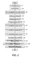
- FIG. 2 is a flowchart showing steps of the method for producing the photoelectric conversion element 10. It should be noted that the method for producing the photoelectric conversion element 10 is not limited to the method illustrated in the steps in FIG. 2 . In each of the steps, for example, a sputtering process, plasma CVD process, screen printing process, plating process, or the like may be used as desired.
- an n-type monocrystalline silicon substrate 18 is prepared, and the light-receiving surface and the backside surface of the n-type monocrystalline silicon substrate 18 are cleaned (S1).
- the n-type monocrystalline silicon substrate 18 may be cleaned using, for example, an HF aqueous solution or the like.
- a texture structure is formed on the light-receiving surface of the n-type monocrystalline silicon substrate 18 (S2).
- the texture structure is formed using, for example, an anisotropic etching solution such as a potassium hydroxide aqueous solution (KOH aqueous solution).
- KOH aqueous solution potassium hydroxide aqueous solution
- the i-type amorphous silicon layer 16 and the n-type amorphous silicon layer 14 are formed on the light-receiving surface of the n-type monocrystalline silicon substrate 18, and the i-type amorphous silicon layer 22a and the n-type amorphous silicon layer 23a are formed on the backside surface of the n-type monocrystalline silicon substrate 18 (S3).
- the i-type amorphous silicon layer 16, the n-type amorphous silicon layer 14, the i-type amorphous silicon layer 22a, and the n-type amorphous silicon layer 23a respectively can be formed by, for example, a plasma CVD process or the like.
- an antireflection layer 12 is formed on the n-type amorphous silicon layer 14 (S4).
- the antireflection layer 12 can be formed by, for example, a thin film formation process such as a sputtering process or plasma CVD process.
- an insulating layer 24a is formed on the n-type amorphous silicon layer 23a (S5).
- the insulating layer 24a can be formed by, for example, a thin film formation process such as a sputtering process or plasma CVD process.
- the insulating layer 24a is etched to partially remove the insulating layer 24a (S6). Specifically, a portion of the insulating layer 24a which is located above a region in which an i-p multilayer portion 31 is formed on the n-type monocrystalline silicon substrate 18 in a later step is removed to form an insulating layer 24b. In this step, the insulating layer 24a is etched using, for example, an acidic etchant such as an HF aqueous solution or the like.
- an acidic etchant such as an HF aqueous solution or the like.
- the i-type amorphous silicon layer 22a and the n-type amorphous silicon layer 23a are etched using the insulating layer 24b patterned in step S6 as a mask (S7). Specifically, a portion of the i-type amorphous silicon layer 22a and the n-type amorphous silicon layer 23a other than that covered by the insulating layer 24b is removed. As a result, a portion of the backside surface of the n-type monocrystalline silicon substrate 18 in which the insulating layer 24b is not located is exposed to form an i-type amorphous silicon layer 22 and an n-type amorphous silicon layer 23.
- the i-type amorphous silicon layer 22a and the n-type amorphous silicon layer 23a are etched using, for example, an alkaline etchant such as an aqueous solution containing sodium hydroxide (NaOH).
- an alkaline etchant such as an aqueous solution containing sodium hydroxide (NaOH).
- an i-type amorphous silicon layer 32a and a p-type amorphous silicon layer 33a are formed to cover the insulating layer 24b, the i-type amorphous silicon layer 22, the n-type amorphous silicon layer 23, and the exposed backside surface of the n-type monocrystalline silicon substrate 18 (S8).
- the i-type amorphous silicon layer 32a and the p-type amorphous silicon layer 33a can be formed by, for example, a plasma CVD process or the like.
- a portion of the i-type amorphous silicon layer 32a and the p-type amorphous silicon layer 33a located above the insulating layer 24b is partially etched (S9).
- an i-type amorphous silicon layer 32b and a p-type amorphous silicon layer 33b are formed.
- the i-type amorphous silicon layer 32a and the p-type amorphous silicon layer 33a are etched using, for example, an alkaline etchant such as an aqueous solution containing sodium hydroxide (NaOH).
- the insulating layer 24b is etched to further partially remove the insulating layer 24b (S10). Specifically, the exposed portion of the insulating layer 24b is removed by etching using the i-type amorphous silicon layer 32b and the p-type amorphous silicon layer 33b as a mask to form an insulating layer 24. In this step, the insulating layer 24b is etched using, for example, an acidic etchant such as an HF aqueous solution.
- an acidic etchant such as an HF aqueous solution.
- a transparent conductive layer 26a and a metal layer 27a are formed (S11).
- the transparent conductive layer 26a and the metal layer 27a are formed by a thin film formation process such as a plasma CVD process or sputtering process.
- a portion of the transparent conductive layer 26a and the metal layer 27a located above the insulating layer 24 is separated to form transparent conductive layers 26 and 36 and metal layers 27 and 37 (S12).
- the transparent conductive layer 26a and the metal layer 27a are separated by, for example, etching using a resist mask.
- a first electrode portion 28 and a second electrode portion 29 are sequentially formed on the metal layer 27, and a first electrode portion 38 and a second electrode portion 39 are sequentially formed on the metal layer 37 by electroplating (S13).
- S13 electroplating
- an interface between the n-type monocrystalline silicon substrate 18 and the i-type amorphous silicon layer 16 and an interface between the n-type monocrystalline silicon substrate 18 and the i-type amorphous silicon layers 22 and 32 be kept clean.
- the degree of contamination on a surface opposite to a surface on which deposition is performed during deposition of the antireflection layer 12 and the insulating layer 24 is greater than that during deposition of the i-type amorphous silicon layers 22 and 32.
- the i-type amorphous silicon layer 16 and the n-type amorphous silicon layer 14 on the light-receiving surface of the n-type monocrystalline silicon substrate 18, depositing the i-type amorphous silicon layer 22 and the n-type amorphous silicon layer 23 on the backside surface of the n-type monocrystalline silicon substrate 18, and, after that, depositing the antireflection layer 12 and the insulating layer 24, the antireflection layer 12 and the insulating layer 24 are deposited after both surfaces of the n-type monocrystalline silicon substrate 18 are covered by at least the i-type amorphous silicon layers 16 and 22.
- the i-type amorphous silicon layers 16, 22, and 32 can be made to suitably serve as a passivation layer, and the power generation characteristics of the photoelectric conversion element 10 can be improved.
- the antireflection layer 12 located on the light-receiving surface side is deposited before the insulating layer 24a located on the backside surface side is deposited.
- the antireflection layer 12 by depositing the antireflection layer 12, the n-type amorphous silicon layer 14 is covered, and a stray stream of a material gas is prevented from reaching the n-type amorphous silicon layer 14 during subsequent deposition of the insulating layer 24a.
- the n-type amorphous silicon layer 14 suitably provides the light confinement effect of the texture structure, the power generation characteristics of the photoelectric conversion element 10 can be improved.
- the antireflection layer 12 typically has a higher mechanical strength than that of the n-type amorphous silicon layer 14.
- the n-type amorphous silicon layer 14 is covered by the antireflection layer 12
- scratches made on the surface of the n-type amorphous silicon layer 14 during the manufacturing process of the photoelectric conversion element 10 can be reduced.
- the n-type amorphous silicon layer 14 suitably provides the light confinement effect of the texture structure, the power generation characteristics of the photoelectric conversion element 10 can be improved.
Landscapes
- Photovoltaic Devices (AREA)
- Life Sciences & Earth Sciences (AREA)
- Engineering & Computer Science (AREA)
- Sustainable Energy (AREA)
- Sustainable Development (AREA)
Abstract
Description
- The present invention relates to a method for producing a photoelectric conversion element.
- Various types of photoelectric conversion elements using monocrystalline silicon, polycrystalline silicon, or amorphous silicon have been developed. As an example, Patent Document 1 discloses a photoelectric conversion element comprising a semiconductor substrate composed of monocrystalline silicon having a light-receiving surface and a backside surface provided opposite to the light-receiving surface; a first semiconductor layer and a second semiconductor layer both composed of amorphous silicon which are formed along a predetermined direction on the backside surface, in which layers having different conductivity types are alternately arranged on the backside surface; an insulating layer formed to span from above the second semiconductor layer to above the first semiconductor layer; a transparent electrode layer covering the first semiconductor layer and the second semiconductor layer; and a collector electrode layer formed on the transparent electrode layer.
- Patent Document 1:
JP 2009-200267 A - In a photoelectric conversion element for generating carriers in a semiconductor substrate, very small projections and depressions (texture) are formed on the light-receiving surface of the semiconductor substrate to cause a scattering of incident light to lengthen the optical path length, so that power generation efficiency is increased. The texture formed on the light-receiving surface of the semiconductor substrate is formed before the first semiconductor layer and the second semiconductor layer (amorphous silicon layers) are formed. As such, the structure having projections and depressions may become deformed through the process of forming an amorphous silicon layer or an insulating layer, which results in a problem in that the effect of scattering incident light cannot be sufficiently achieved.
- According to one aspect of the present invention, there is provided a method for producing a photoelectric conversion element, the method comprising a first step of forming a first amorphous semiconductor layer on a light-receiving surface of a crystalline semiconductor substrate; a second step of forming a second amorphous semiconductor layer on a backside surface of the crystalline semiconductor substrate; and a third step of forming, after completion of the first step and the second step, a protective layer on the first amorphous semiconductor layer, and subsequently forming a protective layer on the second amorphous semiconductor layer.
- By employing the present invention, the power generation characteristics of a photoelectric conversion element can be improved.
-
-
FIG. 1 is a cross-sectional view of a photoelectric conversion element according to an embodiment of the present invention. -
FIG. 2 is a flowchart showing steps of a method for producing a photoelectric conversion element according to the embodiment of the present invention. -
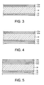
FIG. 3 is a cross-sectional view for illustrating the steps of the method for producing a photoelectric conversion element according to the embodiment of the present invention. -
FIG. 4 is a cross-sectional view for illustrating the steps of the method for producing a photoelectric conversion element according to the embodiment of the present invention. -
FIG. 5 is a cross-sectional view for illustrating the steps of the method for producing a photoelectric conversion element according to the embodiment of the present invention. -
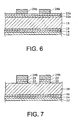
FIG. 6 is a cross-sectional view for illustrating the steps of the method for producing a photoelectric conversion element according to the embodiment of the present invention. -
FIG. 7 is a cross-sectional view for illustrating the steps of the method for producing a photoelectric conversion element according to the embodiment of the present invention. -
FIG. 8 is a cross-sectional view for illustrating the steps of the method for producing a photoelectric conversion element according to the embodiment of the present invention. -
FIG. 9 is a cross-sectional view for illustrating the steps of the method for producing a photoelectric conversion element according to the embodiment of the present invention. -
FIG. 10 is a cross-sectional view for illustrating the steps of the method for producing a photoelectric conversion element according to the embodiment of the present invention. -
FIG. 11 is a cross-sectional view for illustrating the steps of the method for producing a photoelectric conversion element according to the embodiment of the present invention. -
FIG. 12 is a cross-sectional view for illustrating the steps of the method for producing a photoelectric conversion element according to the embodiment of the present invention. -
FIG. 13 is a cross-sectional view for illustrating the steps of the method for producing a photoelectric conversion element according to the embodiment of the present invention. - An embodiment of the present invention will be described in detail below with reference to the drawings. In the following description, similar elements are denoted by the same reference numerals throughout all of the drawings, and the same description will not be repeated. Also, in the description herein, reference numerals used earlier will be used as necessary.
-
FIG. 1 is a cross-sectional view of aphotoelectric conversion element 10. Thephotoelectric conversion element 10 includes anantireflection layer 12, an n-typeamorphous silicon layer 14, an i-typeamorphous silicon layer 16, an n-typemonocrystalline silicon substrate 18, ani-n multilayer portion 21, ani-p multilayer portion 31, aninsulating layer 24, an n-side electrode portion 25, and a p-side electrode portion 35. InFIG. 1 , an arrow A represents the direction in which light such as sunlight is incident on thephotoelectric conversion element 10. It should be noted that the term "light-receiving surface" refers to a surface on which light such as sunlight is mainly incident. Further, the term "backside surface" refers to a surface opposite to the light-receiving surface. - The n-type
monocrystalline silicon substrate 18 is a power generation layer that generates carriers in response to light incident through the light-receiving surface. It should be noted that although the n-typemonocrystalline silicon substrate 18 is used in the present embodiment, the present invention is not limited to this embodiment. A crystalline semiconductor substrate having an n-type or p-type conductivity may be used. Rather than a monocrystalline silicon substrate, for example, a polycrystalline silicon substrate, a gallium arsenide substrate (GaAs), an indium phosphide substrate (InP), or the like may be used. - The i-type
amorphous silicon layer 16 and the n-typeamorphous silicon layer 14 are passivation layers formed on the light-receiving surface of the n-typemonocrystalline silicon substrate 18. The i-typeamorphous silicon layer 16 and the n-typeamorphous silicon layer 14 constitute an amorphous semiconductor layer formed on the light-receiving surface. The i-typeamorphous silicon layer 16 is composed of an intrinsic amorphous semiconductor film. The n-typeamorphous silicon layer 14 is composed of an amorphous semiconductor film containing a dopant having an n-type conductivity. For example, it is preferable that the concentration of the n-type dopant in the n-typeamorphous silicon layer 14 is 1×10²¹/cm3 or higher. - It should be noted that in the present embodiment, the amorphous silicon layers include a microcrystalline semiconductor film. The microcrystalline semiconductor film is a film in which crystal grains are precipitated in an amorphous semiconductor. The average grain size of the crystal grains is estimated to be, but not limited to, not less than about 1 nm and not greater than about 80 nm.
- The
antireflection layer 12 is formed on the n-typeamorphous silicon layer 14, and reduces reflection of light incident through the light-receiving surface of thephotoelectric conversion element 10. Further, theantireflection layer 12 also serves as a protective layer for protecting a surface of the n-typeamorphous silicon layer 14. It is preferable that theantireflection layer 12 is formed of a transparent material, and the material and the film thickness are adjusted such that theantireflection layer 12 has an index of refraction at which reflection of light incident through the light-receiving surface of thephotoelectric conversion element 10 is reduced in relation to the index of refraction of a layer covered by theantireflection layer 12. Theantireflection layer 12 comprises, for example, aluminum oxide, aluminum nitride, silicon nitride, silicon oxide, or the like. - The
i-n multilayer portion 21 is formed on the backside surface of the n-typemonocrystalline silicon substrate 18, and includes an i-typeamorphous silicon layer 22 and an n-typeamorphous silicon layer 23. It is preferable that the i-nmultilayer portion 21 is disposed such that a greater amount of current can be collected from inside the plane of thephotoelectric conversion element 10 in the n-side electrode portion 25 which will be described later. It is preferable that thei-n multilayer portion 21 has, for example, a comb shape in which a plurality of finger portions extend in parallel with each other. - The i-type
amorphous silicon layer 22 is a passivation layer formed on the backside surface of the n-typemonocrystalline silicon substrate 18. The n-typeamorphous silicon layer 23 is formed on the i-typeamorphous silicon layer 22. The i-typeamorphous silicon layer 22 and the n-typeamorphous silicon layer 23 constitute a portion of an amorphous semiconductor layer formed on the backside surface. The i-typeamorphous silicon layer 22 is composed of an intrinsic amorphous semiconductor film. The n-typeamorphous silicon layer 23 is composed of an amorphous semiconductor film containing a dopant having an n-type conductivity. For example, it is preferable that the concentration of the n-type dopant in the n-typeamorphous silicon layer 23 is 1×10²¹/cm3 or higher. - The
insulating layer 24 is formed in order to electrically insulate thei-n multilayer portion 21 and thei-p multilayer portion 31 from each other. Further, theinsulating layer 24 also serves as a protective layer formed on the n-typeamorphous silicon layer 23. Although the insulatinglayer 24 may be any material having an electrically insulating property, it is preferable that the insulatinglayer 24 comprises, for example, aluminum nitride, silicon nitride, silicon oxide, or the like. - The n-
side electrode portion 25 is an electrode component provided to collect and draw out electricity generated in thephotoelectric conversion element 10. The n-side electrode portion 25 includes a transparentconductive layer 26, ametal layer 27, afirst electrode portion 28, and asecond electrode portion 29. - The transparent
conductive layer 26 is formed on the n-typeamorphous silicon layer 23. The transparentconductive layer 26 comprises at least one of metal oxides such as indium oxide (In2O3), zinc oxide (ZnO), tin oxide (SnO2), titanium oxide (TiO2), and indium tin oxide (ITO). In this description, it is assumed that the transparentconductive layer 26 is formed using indium tin oxide (ITO). - The
metal layer 27 is formed on the transparentconductive layer 26. Themetal layer 27 is a seed layer comprising, for example, a metal such as copper (Cu) or an alloy. The term "seed layer" as used herein refers to a layer from which plating growth starts. - The
first electrode portion 28 is an electrode formed on themetal layer 27 by plating. Thefirst electrode portion 28 comprises, for example, copper (Cu). - The
second electrode portion 29 is an electrode formed on thefirst electrode portion 28 by plating. Thesecond electrode portion 29 comprises, for example, tin (Sn). - The
i-p multilayer portion 31 is formed such that thei-p multilayer portion 31 and thei-n multilayer portion 21 are alternately arranged on the backside surface of the n-typemonocrystalline silicon substrate 18. Thei-p multilayer portion 31 includes an i-typeamorphous silicon layer 32 and a p-typeamorphous silicon layer 33. It is preferable that thei-p multilayer portion 31 is disposed such that a greater amount of current can be collected from inside the plane of thephotoelectric conversion element 10 in the p-side electrode portion 35 which will be described later. It is preferable that thei-p multilayer portion 31 has, for example, a comb shape in which a plurality of finger portions extend parallel with each other. - The i-type
amorphous silicon layer 32 is a passivation layer formed on the backside surface of the n-typemonocrystalline silicon substrate 18. The p-typeamorphous silicon layer 33 is formed on the i-typeamorphous silicon layer 32. The i-typeamorphous silicon layer 32 and the p-typeamorphous silicon layer 33 constitute a portion of an amorphous semiconductor layer formed on the backside surface. The i-typeamorphous silicon layer 32 is composed of an intrinsic amorphous semiconductor film. The p-typeamorphous silicon layer 33 is composed of an amorphous semiconductor film containing a dopant having a p-type conductivity. For example, it is preferable that the concentration of the p-type dopant in the p-typeamorphous silicon layer 33 is 1×10²¹/cm3 or higher. - The p-
side electrode portion 35 is an electrode component provided to collect and draw out electricity generated in thephotoelectric conversion element 10. The p-side electrode portion 35 includes a transparentconductive layer 36, ametal layer 37, afirst electrode portion 38, and asecond electrode portion 39. - The transparent
conductive layer 36 is formed on the p-typeamorphous silicon layer 33. Themetal layer 37, thefirst electrode portion 38, and thesecond electrode portion 39 are formed on the transparentconductive layer 36. As the materials and other features for the transparentconductive layer 36, themetal layer 37, thefirst electrode portion 38, and thesecond electrode portion 39 are the same as for the transparentconductive layer 26, themetal layer 27, thefirst electrode portion 28, and thesecond electrode portion 29, detailed description is not repeated here. - Next, an example of a method for producing the
photoelectric conversion element 10 will be described below. -
FIG. 2 is a flowchart showing steps of the method for producing thephotoelectric conversion element 10. It should be noted that the method for producing thephotoelectric conversion element 10 is not limited to the method illustrated in the steps inFIG. 2 . In each of the steps, for example, a sputtering process, plasma CVD process, screen printing process, plating process, or the like may be used as desired. - First, an n-type
monocrystalline silicon substrate 18 is prepared, and the light-receiving surface and the backside surface of the n-typemonocrystalline silicon substrate 18 are cleaned (S1). In this step, the n-typemonocrystalline silicon substrate 18 may be cleaned using, for example, an HF aqueous solution or the like. - Next, a texture structure is formed on the light-receiving surface of the n-type monocrystalline silicon substrate 18 (S2). In this step, the texture structure is formed using, for example, an anisotropic etching solution such as a potassium hydroxide aqueous solution (KOH aqueous solution). As a result, a shape having pyramidal projections and depressions can be formed on the light-receiving surface of the n-type
monocrystalline silicon substrate 18. - Then, as shown in
FIG. 3 , the i-typeamorphous silicon layer 16 and the n-typeamorphous silicon layer 14 are formed on the light-receiving surface of the n-typemonocrystalline silicon substrate 18, and the i-typeamorphous silicon layer 22a and the n-typeamorphous silicon layer 23a are formed on the backside surface of the n-type monocrystalline silicon substrate 18 (S3). In this step, the i-typeamorphous silicon layer 16, the n-typeamorphous silicon layer 14, the i-typeamorphous silicon layer 22a, and the n-typeamorphous silicon layer 23a respectively can be formed by, for example, a plasma CVD process or the like. - Subsequently, as shown in
FIG. 4 , anantireflection layer 12 is formed on the n-type amorphous silicon layer 14 (S4). Theantireflection layer 12 can be formed by, for example, a thin film formation process such as a sputtering process or plasma CVD process. - After that, as shown in
FIG. 5 , an insulatinglayer 24a is formed on the n-typeamorphous silicon layer 23a (S5). The insulatinglayer 24a can be formed by, for example, a thin film formation process such as a sputtering process or plasma CVD process. - Next, as shown in
FIG. 6 , the insulatinglayer 24a is etched to partially remove the insulatinglayer 24a (S6). Specifically, a portion of the insulatinglayer 24a which is located above a region in which ani-p multilayer portion 31 is formed on the n-typemonocrystalline silicon substrate 18 in a later step is removed to form an insulatinglayer 24b. In this step, the insulatinglayer 24a is etched using, for example, an acidic etchant such as an HF aqueous solution or the like. - Then, as shown in
FIG. 7 , the i-typeamorphous silicon layer 22a and the n-typeamorphous silicon layer 23a are etched using the insulatinglayer 24b patterned in step S6 as a mask (S7). Specifically, a portion of the i-typeamorphous silicon layer 22a and the n-typeamorphous silicon layer 23a other than that covered by the insulatinglayer 24b is removed. As a result, a portion of the backside surface of the n-typemonocrystalline silicon substrate 18 in which the insulatinglayer 24b is not located is exposed to form an i-typeamorphous silicon layer 22 and an n-typeamorphous silicon layer 23. In this step, the i-typeamorphous silicon layer 22a and the n-typeamorphous silicon layer 23a are etched using, for example, an alkaline etchant such as an aqueous solution containing sodium hydroxide (NaOH). - Subsequently, as shown in
FIG. 8 , an i-typeamorphous silicon layer 32a and a p-typeamorphous silicon layer 33a are formed to cover the insulatinglayer 24b, the i-typeamorphous silicon layer 22, the n-typeamorphous silicon layer 23, and the exposed backside surface of the n-type monocrystalline silicon substrate 18 (S8). The i-typeamorphous silicon layer 32a and the p-typeamorphous silicon layer 33a can be formed by, for example, a plasma CVD process or the like. - After that, as shown in
FIG. 9 , a portion of the i-typeamorphous silicon layer 32a and the p-typeamorphous silicon layer 33a located above the insulatinglayer 24b is partially etched (S9). As a result, an i-typeamorphous silicon layer 32b and a p-typeamorphous silicon layer 33b are formed. In this step, the i-typeamorphous silicon layer 32a and the p-typeamorphous silicon layer 33a are etched using, for example, an alkaline etchant such as an aqueous solution containing sodium hydroxide (NaOH). - Next, as shown in
FIG. 10 , the insulatinglayer 24b is etched to further partially remove the insulatinglayer 24b (S10). Specifically, the exposed portion of the insulatinglayer 24b is removed by etching using the i-typeamorphous silicon layer 32b and the p-typeamorphous silicon layer 33b as a mask to form an insulatinglayer 24. In this step, the insulatinglayer 24b is etched using, for example, an acidic etchant such as an HF aqueous solution. - Then, as shown in
FIG. 11 , a transparentconductive layer 26a and ametal layer 27a are formed (S11). Specifically, the transparentconductive layer 26a and themetal layer 27a are formed by a thin film formation process such as a plasma CVD process or sputtering process. - Subsequently, as shown in
FIG. 12 , a portion of the transparentconductive layer 26a and themetal layer 27a located above the insulatinglayer 24 is separated to form transparentconductive layers metal layers 27 and 37 (S12). In this step, the transparentconductive layer 26a and themetal layer 27a are separated by, for example, etching using a resist mask. - After that, as shown in
FIG. 13 , afirst electrode portion 28 and asecond electrode portion 29 are sequentially formed on themetal layer 27, and afirst electrode portion 38 and asecond electrode portion 39 are sequentially formed on themetal layer 37 by electroplating (S13). As a result, an n-side electrode portion 25 and a p-side electrode portion 35 are formed. - Typically, in order to prevent recombination of carriers generated in the n-type
monocrystalline silicon substrate 18 of thephotoelectric conversion element 10, it is preferable that an interface between the n-typemonocrystalline silicon substrate 18 and the i-typeamorphous silicon layer 16, and an interface between the n-typemonocrystalline silicon substrate 18 and the i-type amorphous silicon layers 22 and 32, be kept clean. In this regard, due to, for example, the difference in degree of vacuum during deposition or a stray stream of a material gas, the degree of contamination on a surface opposite to a surface on which deposition is performed during deposition of theantireflection layer 12 and the insulatinglayer 24 is greater than that during deposition of the i-type amorphous silicon layers 22 and 32. In consideration of the above, according to the present embodiment, by depositing the i-typeamorphous silicon layer 16 and the n-typeamorphous silicon layer 14 on the light-receiving surface of the n-typemonocrystalline silicon substrate 18, depositing the i-typeamorphous silicon layer 22 and the n-typeamorphous silicon layer 23 on the backside surface of the n-typemonocrystalline silicon substrate 18, and, after that, depositing theantireflection layer 12 and the insulatinglayer 24, theantireflection layer 12 and the insulatinglayer 24 are deposited after both surfaces of the n-typemonocrystalline silicon substrate 18 are covered by at least the i-type amorphous silicon layers 16 and 22. As a result, contamination of the interfaces between the n-typemonocrystalline silicon substrate 18 and the i-type amorphous silicon layers 16, 22, and 32 during deposition of theantireflection layer 12 and the insulatinglayer 24 is prevented. As such, the i-type amorphous silicon layers 16, 22, and 32 can be made to suitably serve as a passivation layer, and the power generation characteristics of thephotoelectric conversion element 10 can be improved. - Further, in terms of the order in which the
antireflection layer 12 and the insulatinglayer 24 are deposited, theantireflection layer 12 located on the light-receiving surface side is deposited before the insulatinglayer 24a located on the backside surface side is deposited. In other words, by depositing theantireflection layer 12, the n-typeamorphous silicon layer 14 is covered, and a stray stream of a material gas is prevented from reaching the n-typeamorphous silicon layer 14 during subsequent deposition of the insulatinglayer 24a. As a result, presence of the above-described contaminant on the texture structure of the n-typeamorphous silicon layer 14 is prevented. As such, as the n-typeamorphous silicon layer 14 suitably provides the light confinement effect of the texture structure, the power generation characteristics of thephotoelectric conversion element 10 can be improved. - Still further, the
antireflection layer 12 typically has a higher mechanical strength than that of the n-typeamorphous silicon layer 14. As a result, as the n-typeamorphous silicon layer 14 is covered by theantireflection layer 12, scratches made on the surface of the n-typeamorphous silicon layer 14 during the manufacturing process of thephotoelectric conversion element 10 can be reduced. As such, as the n-typeamorphous silicon layer 14 suitably provides the light confinement effect of the texture structure, the power generation characteristics of thephotoelectric conversion element 10 can be improved. -
- 10 PHOTOELECTRIC CONVERSION ELEMENT
- 12, 24, 24a, 24b INSULATING LAYER
- 14, 23, 23a N-TYPE AMORPHOUS SILICON LAYER
- 16, 22, 22a, 32, 32a, 32b I-TYPE AMORPHOUS SILICON LAYER
- 18 N-TYPE MONOCRYSTALLINE SILICON SUBSTRATE
- 21 I-N MULTILAYER PORTION
- 25 N-SIDE ELECTRODE PORTION
- 26, 26a, 36 TRANSPARENT CONDUCTIVE LAYER
- 27, 27a, 37 METAL LAYER
- 28, 38 FIRST ELECTRODE PORTION
- 29, 39 SECOND ELECTRODE PORTION
- 31 I-P MULTILAYER PORTION
- 33, 33a, 33b P-TYPE AMORPHOUS SILICON LAYER
- 35 P-SIDE ELECTRODE PORTION
Claims (4)
- A method for producing a photoelectric conversion element, the method comprising:a first step of forming a first amorphous semiconductor layer on a light-receiving surface of a crystalline semiconductor substrate;a second step of forming a second amorphous semiconductor layer on a backside surface of the crystalline semiconductor substrate; anda third step of forming, after completion of the first step and the second step, a protective layer on the first amorphous semiconductor layer, and subsequently forming a protective layer on the second amorphous semiconductor layer.
- The method for producing a photoelectric conversion element according to claim 1, wherein
the crystalline semiconductor substrate is of n-type,
the first amorphous semiconductor layer comprises:a first i-type amorphous semiconductor layer formed on the light-receiving surface of the crystalline semiconductor substrate; anda first n-type amorphous semiconductor layer formed on the first i-type amorphous semiconductor layer, andthe second amorphous semiconductor layer comprises:a second i-type amorphous semiconductor layer formed on the backside surface of the crystalline semiconductor substrate; anda second n-type amorphous semiconductor layer formed on the second i-type amorphous semiconductor layer. - The method for producing a photoelectric conversion element according to claim 2, the photoelectric conversion element comprising:a first electrode portion formed in a first region located above the second n-type amorphous semiconductor layer; anda second electrode portion formed in a second region located above a second p-type amorphous semiconductor layer formed on the backside surface, the second region being different from the first region.
- The method for producing a photoelectric conversion element according to any one of claims 1 to 3, wherein
the protective layer comprises one of aluminum oxide, aluminum nitride, silicon nitride, and silicon oxide.
Applications Claiming Priority (2)
| Application Number | Priority Date | Filing Date | Title |
|---|---|---|---|
| JP2011068311 | 2011-03-25 | ||
| PCT/JP2012/056867 WO2012132961A1 (en) | 2011-03-25 | 2012-03-16 | Method for producing photoelectric conversion element |
Publications (2)
| Publication Number | Publication Date |
|---|---|
| EP2690668A1 true EP2690668A1 (en) | 2014-01-29 |
| EP2690668A4 EP2690668A4 (en) | 2014-09-03 |
Family
ID=46930694
Family Applications (1)
| Application Number | Title | Priority Date | Filing Date |
|---|---|---|---|
| EP12765778.1A Withdrawn EP2690668A4 (en) | 2011-03-25 | 2012-03-16 | METHOD FOR PRODUCING PHOTOELECTRIC CONVERSION ELEMENT |
Country Status (4)
| Country | Link |
|---|---|
| US (1) | US9070822B2 (en) |
| EP (1) | EP2690668A4 (en) |
| JP (1) | JP5820989B2 (en) |
| WO (1) | WO2012132961A1 (en) |
Families Citing this family (4)
| Publication number | Priority date | Publication date | Assignee | Title |
|---|---|---|---|---|
| EP2690666A4 (en) * | 2011-03-25 | 2014-09-03 | Sanyo Electric Co | METHOD FOR MANUFACTURING PHOTOELECTRIC CONVERSION ELEMENT |
| JP6104037B2 (en) * | 2013-05-02 | 2017-03-29 | 三菱電機株式会社 | Photovoltaic device, manufacturing method thereof, and photovoltaic module |
| JP2015053303A (en) * | 2013-09-05 | 2015-03-19 | シャープ株式会社 | Solar cell, solar cell module, and method for manufacturing solar cell. |
| JP6369680B2 (en) * | 2014-05-30 | 2018-08-08 | パナソニックIpマネジメント株式会社 | Solar cell |
Family Cites Families (11)
| Publication number | Priority date | Publication date | Assignee | Title |
|---|---|---|---|---|
| US4626878A (en) * | 1981-12-11 | 1986-12-02 | Sanyo Electric Co., Ltd. | Semiconductor optical logical device |
| JP2001189478A (en) * | 1999-12-28 | 2001-07-10 | Sanyo Electric Co Ltd | Semiconductor device and manufacturing method thereof |
| US7307940B2 (en) * | 2003-06-30 | 2007-12-11 | Semiconductor Energy Laboratory Co., Ltd. | Optical pick-up device |
| JP2005159171A (en) * | 2003-11-27 | 2005-06-16 | Kyocera Corp | Solar cell element and manufacturing method thereof |
| JP4716881B2 (en) * | 2006-01-24 | 2011-07-06 | 信越半導体株式会社 | Manufacturing method of solar cell |
| JP5230222B2 (en) | 2008-02-21 | 2013-07-10 | 三洋電機株式会社 | Solar cell |
| WO2010113750A1 (en) * | 2009-03-30 | 2010-10-07 | 三洋電機株式会社 | Solar cell |
| US7927910B2 (en) * | 2009-06-28 | 2011-04-19 | Sino-American Silicon Products Inc. | Manufacturing method of solar cell |
| JP2011035092A (en) * | 2009-07-31 | 2011-02-17 | Sanyo Electric Co Ltd | Back-junction type solar cell and solar cell module using the same |
| EP2293351B1 (en) * | 2009-09-07 | 2017-04-12 | Lg Electronics Inc. | Solar cell |
| FR2953999B1 (en) * | 2009-12-14 | 2012-01-20 | Total Sa | PHOTOVOLTAIC CELL HETEROJUNCTION WITH REAR CONTACT |
-
2012
- 2012-03-16 WO PCT/JP2012/056867 patent/WO2012132961A1/en not_active Ceased
- 2012-03-16 EP EP12765778.1A patent/EP2690668A4/en not_active Withdrawn
- 2012-03-16 JP JP2013507387A patent/JP5820989B2/en not_active Expired - Fee Related
-
2013
- 2013-09-25 US US14/036,847 patent/US9070822B2/en not_active Expired - Fee Related
Also Published As
| Publication number | Publication date |
|---|---|
| EP2690668A4 (en) | 2014-09-03 |
| JPWO2012132961A1 (en) | 2014-07-28 |
| JP5820989B2 (en) | 2015-11-24 |
| WO2012132961A1 (en) | 2012-10-04 |
| US9070822B2 (en) | 2015-06-30 |
| US20140024167A1 (en) | 2014-01-23 |
Similar Documents
| Publication | Publication Date | Title |
|---|---|---|
| US9257593B2 (en) | Method for producing photoelectric conversion element | |
| JP5879538B2 (en) | Photoelectric conversion device and manufacturing method thereof | |
| EP2219222B1 (en) | Solar cell and method for manufacturing the same | |
| JP5705968B2 (en) | Photoelectric conversion device and manufacturing method thereof | |
| KR101863294B1 (en) | Solar cell and method for fabricating the same | |
| CN110010720A (en) | The manufacturing method and solar energy monocell of solar energy monocell | |
| KR20120031630A (en) | Semiconductor device and manufacturing method thereof | |
| KR20130067208A (en) | Photovoltaic device and its manufacturing method | |
| TWI590478B (en) | Solar cell and solar cell manufacturing method | |
| CN111834475A (en) | Solar cells and solar modules | |
| CN102947947B (en) | Photoelectric conversion device | |
| US9070822B2 (en) | Method for producing photoelectric conversion element | |
| US20140024168A1 (en) | Method for producing photoelectric conversion device | |
| US11177407B2 (en) | Method for manufacturing solar cell, solar cell, and solar cell module | |
| US20140020741A1 (en) | Solar cell and method for producing solar cell | |
| WO2012132614A1 (en) | Photoelectric converter | |
| JP5351628B2 (en) | Crystalline silicon solar cell | |
| CN110098266A (en) | The manufacturing method of solar energy monocell and solar energy monocell | |
| JP2013098390A (en) | Photoelectric transducer, manufacturing method thereof, and photoelectric conversion module |
Legal Events
| Date | Code | Title | Description |
|---|---|---|---|
| PUAI | Public reference made under article 153(3) epc to a published international application that has entered the european phase |
Free format text: ORIGINAL CODE: 0009012 |
|
| 17P | Request for examination filed |
Effective date: 20130918 |
|
| AK | Designated contracting states |
Kind code of ref document: A1 Designated state(s): AL AT BE BG CH CY CZ DE DK EE ES FI FR GB GR HR HU IE IS IT LI LT LU LV MC MK MT NL NO PL PT RO RS SE SI SK SM TR |
|
| DAX | Request for extension of the european patent (deleted) | ||
| A4 | Supplementary search report drawn up and despatched |
Effective date: 20140806 |
|
| RIC1 | Information provided on ipc code assigned before grant |
Ipc: H01L 31/0224 20060101ALI20140731BHEP Ipc: H01L 31/0747 20120101ALI20140731BHEP Ipc: H01L 31/04 20140101AFI20140731BHEP Ipc: H01L 31/0352 20060101ALI20140731BHEP Ipc: H01L 31/20 20060101ALI20140731BHEP Ipc: H01L 31/068 20120101ALI20140731BHEP |
|
| RAP1 | Party data changed (applicant data changed or rights of an application transferred) |
Owner name: PANASONIC INTELLECTUAL PROPERTY MANAGEMENT CO., LT |
|
| STAA | Information on the status of an ep patent application or granted ep patent |
Free format text: STATUS: THE APPLICATION IS DEEMED TO BE WITHDRAWN |
|
| 18D | Application deemed to be withdrawn |
Effective date: 20161001 |