EP2689437B1 - Tabless roll capacitor and capacitor stack - Google Patents
Tabless roll capacitor and capacitor stack Download PDFInfo
- Publication number
- EP2689437B1 EP2689437B1 EP12761246.3A EP12761246A EP2689437B1 EP 2689437 B1 EP2689437 B1 EP 2689437B1 EP 12761246 A EP12761246 A EP 12761246A EP 2689437 B1 EP2689437 B1 EP 2689437B1
- Authority
- EP
- European Patent Office
- Prior art keywords
- capacitor
- capacitors
- roll
- stack
- strips
- Prior art date
- Legal status (The legal status is an assumption and is not a legal conclusion. Google has not performed a legal analysis and makes no representation as to the accuracy of the status listed.)
- Active
Links
Images




Classifications
-
- H—ELECTRICITY
- H01—ELECTRIC ELEMENTS
- H01G—CAPACITORS; CAPACITORS, RECTIFIERS, DETECTORS, SWITCHING DEVICES, LIGHT-SENSITIVE OR TEMPERATURE-SENSITIVE DEVICES OF THE ELECTROLYTIC TYPE
- H01G4/00—Fixed capacitors; Processes of their manufacture
- H01G4/002—Details
- H01G4/018—Dielectrics
- H01G4/06—Solid dielectrics
-
- H—ELECTRICITY
- H01—ELECTRIC ELEMENTS
- H01G—CAPACITORS; CAPACITORS, RECTIFIERS, DETECTORS, SWITCHING DEVICES, LIGHT-SENSITIVE OR TEMPERATURE-SENSITIVE DEVICES OF THE ELECTROLYTIC TYPE
- H01G4/00—Fixed capacitors; Processes of their manufacture
- H01G4/002—Details
-
- H—ELECTRICITY
- H01—ELECTRIC ELEMENTS
- H01G—CAPACITORS; CAPACITORS, RECTIFIERS, DETECTORS, SWITCHING DEVICES, LIGHT-SENSITIVE OR TEMPERATURE-SENSITIVE DEVICES OF THE ELECTROLYTIC TYPE
- H01G4/00—Fixed capacitors; Processes of their manufacture
- H01G4/002—Details
- H01G4/005—Electrodes
-
- H—ELECTRICITY
- H01—ELECTRIC ELEMENTS
- H01G—CAPACITORS; CAPACITORS, RECTIFIERS, DETECTORS, SWITCHING DEVICES, LIGHT-SENSITIVE OR TEMPERATURE-SENSITIVE DEVICES OF THE ELECTROLYTIC TYPE
- H01G4/00—Fixed capacitors; Processes of their manufacture
- H01G4/002—Details
- H01G4/005—Electrodes
- H01G4/01—Form of self-supporting electrodes
-
- H—ELECTRICITY
- H01—ELECTRIC ELEMENTS
- H01G—CAPACITORS; CAPACITORS, RECTIFIERS, DETECTORS, SWITCHING DEVICES, LIGHT-SENSITIVE OR TEMPERATURE-SENSITIVE DEVICES OF THE ELECTROLYTIC TYPE
- H01G4/00—Fixed capacitors; Processes of their manufacture
- H01G4/002—Details
- H01G4/228—Terminals
- H01G4/232—Terminals electrically connecting two or more layers of a stacked or rolled capacitor
-
- H—ELECTRICITY
- H01—ELECTRIC ELEMENTS
- H01G—CAPACITORS; CAPACITORS, RECTIFIERS, DETECTORS, SWITCHING DEVICES, LIGHT-SENSITIVE OR TEMPERATURE-SENSITIVE DEVICES OF THE ELECTROLYTIC TYPE
- H01G4/00—Fixed capacitors; Processes of their manufacture
- H01G4/30—Stacked capacitors
-
- H—ELECTRICITY
- H01—ELECTRIC ELEMENTS
- H01G—CAPACITORS; CAPACITORS, RECTIFIERS, DETECTORS, SWITCHING DEVICES, LIGHT-SENSITIVE OR TEMPERATURE-SENSITIVE DEVICES OF THE ELECTROLYTIC TYPE
- H01G4/00—Fixed capacitors; Processes of their manufacture
- H01G4/32—Wound capacitors
-
- H—ELECTRICITY
- H01—ELECTRIC ELEMENTS
- H01G—CAPACITORS; CAPACITORS, RECTIFIERS, DETECTORS, SWITCHING DEVICES, LIGHT-SENSITIVE OR TEMPERATURE-SENSITIVE DEVICES OF THE ELECTROLYTIC TYPE
- H01G4/00—Fixed capacitors; Processes of their manufacture
- H01G4/38—Multiple capacitors, i.e. structural combinations of fixed capacitors
Definitions
- the invention relates generally to roll capacitors and to capacitor stacks formed of a plurality of roll capacitors, and more particularly, to roll capacitors connected in parallel and/or series for capacitor voltage transformers, and to assembly thereof.
- Roll capacitors are formed by rolling two electrode strips separated by dielectric strips. This forms a more compact capacitor than a flat plate capacitor with equivalent capacitance.
- Capacitor chains can be made by stacking multiple roll capacitors, then interconnecting them with conductive tabs that extend beyond the ends of the capacitors between respective electrode strips in adjacent rolls. This is seen for example in Figure 4 of United States patent 3,508,128 and in Figure 2 of United States patent 4,623,953 .
- Capacitor chains are used, for example, in capacitor voltage transformers and other applications in the Medium to Ultra-High Voltage system applications, such as: instrument transformers (protection, supervisory control, data acquisition, metering and harmonics monitoring), power line carrier, system network compensation, voltage dividers and tuned filter applications, for example.
- FIG 1 shows a roll capacitor 20A with inner and outer electrode strips 21, 23 separated by inner and outer dielectric strips 22, 24.
- the designations “inner” and “outer” are best seen at the innermost lap 25 of the strips, since both electrodes 21, 23 and both dielectrics 22, 24 are finally “outer” on different parts of the roll outer surface.
- the electrodes 21, 23 are designated with charges + or - for convenience only to show relative charges in each embodiment. These designations are reversible.
- the electrodes 23, 21 have exposed end portions 23E, 21E on opposite sides 26, 28 of the roll 20A for electrical contact.
- the term "side” of a roll herein means a portion of the outer surface of the roll facing in a given direction, such as first and second sides 26, 28 in the figures.
Landscapes
- Engineering & Computer Science (AREA)
- Power Engineering (AREA)
- Manufacturing & Machinery (AREA)
- Microelectronics & Electronic Packaging (AREA)
- Fixed Capacitors And Capacitor Manufacturing Machines (AREA)
Description
- The invention relates generally to roll capacitors and to capacitor stacks formed of a plurality of roll capacitors, and more particularly, to roll capacitors connected in parallel and/or series for capacitor voltage transformers, and to assembly thereof.
- Roll capacitors are formed by rolling two electrode strips separated by dielectric strips. This forms a more compact capacitor than a flat plate capacitor with equivalent capacitance. Capacitor chains can be made by stacking multiple roll capacitors, then interconnecting them with conductive tabs that extend beyond the ends of the capacitors between respective electrode strips in adjacent rolls. This is seen for example in
Figure 4 of United States patent3,508,128 and inFigure 2 of United States patent4,623,953 . Capacitor chains are used, for example, in capacitor voltage transformers and other applications in the Medium to Ultra-High Voltage system applications, such as: instrument transformers (protection, supervisory control, data acquisition, metering and harmonics monitoring), power line carrier, system network compensation, voltage dividers and tuned filter applications, for example. -
FR2343321 FR2129241 US2531185 each describe roll capacitors according to the introductory portion of appendedclaim 1. - The invention is explained In the following description in view of the drawings that show:
-
FIG. 1 is a sectional end view of a roll capacitor in a first embodiment of the invention. -
FIG. 2 shows a stack of roll capacitors of the first embodiment. -
FIG. 3 shows an electrical diagram of the stack ofFIG 2 . -
FIG. 4 shows a stack of roll capacitors with shorter dielectric strips than inFIG 2 . -
FIG. 5 is a sectional end view of a roll capacitor of a second embodiment. -
FIG. 6 shows a stack of capacitors of the second embodiment. -
FIG. 7 shows an electrical diagram of the stack ofFIG 6 . -
FIG. 8 is a sectional end view of a roll capacitor of a third embodiment. -
FIG. 9 shows a stack of capacitors of the second and third embodiments. -
FIG. 10 shows an electrical diagram of the stack ofFIG 9 . -
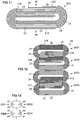
FIG. 11 is a sectional end view of a roll capacitor of a fourth embodiment. -
FIG. 12 shows a stack of capacitors of the fourth embodiment. -
FIG. 13 shows an electrical diagram of the stack ofFIG 12 . -
FIG. 14 shows a stack of capacitors of the third and fourth embodiments. -
FIG. 15 shows an electrical diagram of the stack ofFIG 14 . -
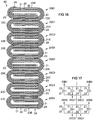
FIG. 16 shows a stack of capacitors of the second and third embodiments. -
FIG. 17 shows an electrical diagram of the stack ofFIG 16 . -
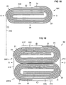
FIG. 18 is a sectional end view of a roll capacitor not according to the present invention. -
FIG. 19 shows a unit of two capacitors each as shown inFig. 18 . -
FIG. 20 is a perspective view of a capacitor of the first embodiment. -
FIG. 21 shows a bound stack of capacitors. - The present inventors have recognized that assembling and interconnecting the conductive tabs of roll capacitors to form capacitor chains is labour intensive, slow, expensive, and subject to human error. The tabs are subject to mechanical stress and cyclic thermal expansion that can fatigue and weaken the electrode strips and dielectric strips. The tabs extend beyond the footprint of the capacitors, thus requiring additional chamber width when enclosed within a porcelain insulator or other containment housing, such as is common for capacitor voltage transformer applications. An improved capacitor design useful for forming capacitor chains is disclosed herein.
-
FIG 1 shows aroll capacitor 20A with inner andouter electrode strips dielectric strips innermost lap 25 of the strips, since bothelectrodes dielectrics electrodes electrodes end portions opposite sides roll 20A for electrical contact. The term "side" of a roll herein means a portion of the outer surface of the roll facing in a given direction, such as first andsecond sides capacitors 20A inherently interconnect by direct stacking contact between the exposedends FIG 2 . No interconnection tabs are needed as are needed in the prior art. -
Capacitor embodiment 20A may be described as a roll of fouradjacent strips inner electrode 21, an inner dielectric 22, anouter electrode 23, and an outer dielectric 24. In general, the roll capacitors herein may be described as a roll of fouradjacent strips electrode strips outer ends side dielectric strip outer end dielectric strips electrode strips -
FIG 2 shows a stack of three electrically interconnected capacitors 20A1, 20A2, and 20A3.FIG 3 shows an electrical diagram of the stack ofFIG 2 . Capacitors 20A1, 20A2, and 20A3 are connected in series. Theinner electrode 21 of each roll contacts theouter electrode 23 of the next roll in the stack. A gap G betweenadjacent contacts stack 50 and others herein, but this gap is eliminated by compressing the stack vertically in a chamber as later described.FIG 4 shows astack 51 of two roll capacitors 20A1 and 20A2 withdielectric strips FIG 2 , eliminating the gap G that is seen isFIG 2 . -
FIG 5 shows aroll capacitor 20B with inner andouter electrode strips dielectric strips electrodes end portions opposite sides roll 20B for electrical contact. This provides inherent electrical interconnection of thecapacitors 20B when they are stacked. In addition, theouter electrode 23 is exposed on bothsides adjacent rolls 20B in one orientation, and a parallel connection in another orientation. -
FIG 6 shows astack 52 of four electrically interconnected roll capacitors 20B1, 20B2, 20B3 and 20B4. Each capacitor is inverted with respect to the previous capacitor in the stack. Thesecond sides 28 of capacitors 20B1 and 20B2 are in mutual contact, such thatelectrodes electrodes inner electrode 21 of capacitor 20B1 contacts theouter electrode 23 of capacitor 20B2, and theouter electrode 23 of 20B1 contacts theinner electrode 21 of 20B2, creating a parallel connection between them. Capacitor 20B3 is inverted with respect to 20B2 such that their respectivefirst sides 26 are in mutual contact. In this orientation, capacitors 20B2 and 20B3 are connected in series. Capacitor 20B4 is inverted with respect to 20B3 such that they are connected in parallel, as described above for the connection between 20B1 and 20B2. The circuit resulting from thestack 52 ofFIG 6 is illustrated inFIG 7 .Capacitor embodiment 20B allows connecting any two adjacent capacitors either in series or in parallel. If more than two capacitors in a row are to be connected in series or parallel, this can be done with other embodiments herein, either alone or in combination withembodiment 20B. -
FIG 8 shows aroll capacitor 20C with inner and outer electrode strips 21, 23, alternating with inner and outer dielectric strips 22, 24. Bothelectrodes end portions opposite sides roll 20B for electrical contact. Capacitors of thistype 20C may be stacked by placing thesecond side 28 of a first capacitor 20C1 against thefirst side 26 of a second capacitor 20C2, creating a parallel interconnection. -
FIG 9 shows astack 54 of four electrically interconnected roll capacitors 20B1, 20C1, 20C2 and 20B4. This stack has parallel connections between 20B1 and 20C1, between 20C1 and 20C2, and between 20C2 and 20B2 as shown inFIG 10 . Any number ofcapacitors 20C may be interconnected in parallel by stacking them as per 20C1 and 20C2. Each end of a stack of capacitors oftype 20C can be finished with acapacitor 20B as shown by 20B1 and 20B2. This arrangement provides a single respective + or - contact at each end of thestack 54 for circuit connections, which can alternately be used for a series connection to additional capacitors as later shown. Capacitor 20B2 is inverted with respect to capacitor 20B1 in thisstack arrangement 54. -
FIG 11 shows aroll capacitor 20D with inner and outer electrode strips 21, 23, alternating with inner and outer dielectric strips 22, 24. Bothelectrodes end portions first side 26 of theroll 20D for electrical contact. Theend portion 21E of one of theelectrodes 21 also is also exposed on thesecond side 28 of the roll. Capacitors of thistype 20D may be stacked in a parallel pair or a sequential pair.Capacitor 20D ofFIG 11 is similar tocapacitor 20B ofFIG 5 in that they both expose both electrodes on one side and only one electrode on the other side. However, they are different in that the one electrode exposed on the other side is theouter electrode 23 incapacitor 20B whereas it is theinner electrode 21 incapacitor 20D. -
FIG 12 shows astack 56 of four electrically interconnected roll capacitors 20D1, 20D2, 20D3 and 20D4. Each capacitor is inverted with respect to the previous capacitor in the stack. The first sides 26 of capacitors 20D1 and 20D2 are in mutual contact, such that bothelectrodes electrodes inner electrode 21 of capacitor 20D1 contacts theouter electrode 23 of capacitor 20D2, and theouter electrode 23 of 20D1 contacts theinner electrode 21 of 20D2, creating a parallel connection between them as shown inFIG 13 . Capacitor 20D3 is inverted with respect to 20D2 such that theirsecond sides 28 are in mutual contact. In this orientation, capacitors 20D2 and 20D3 are connected in series.Capacitor embodiment 20D allows connecting any two adjacent capacitors either in series or in parallel. If more than two capacitors in a row are to be connected in series or parallel, other embodiments herein, either alone or in combination withembodiment 20D may be used. -
FIG 14 shows astack 58 of four electrically interconnected roll capacitors 20D1, 20C1, 20C2 and 20D4. This stack has parallel connections between 20B1 and 20C1, and between 20C1 and 20C2, and between 20C2 and 20B2 as shown inFIG 15 . Any number of capacitors oftype 20C may be interconnected in parallel by stacking them per 20C1 and 20C2. Each end of a stack of capacitors oftype 20C can be finished with acapacitor 20D as shown by 20D1 and 20D2. This arrangement provides a single respective + or - stack end contact for circuit connections at each end of thestack 56. Either or both stack end contacts can alternately be used for a series connection to additional capacitors as later shown. Capacitor 20D2 is inverted with respect to capacitor 20D1 in thisstack arrangement 58. Gaps G are eliminated by compression of thestack 56 when installed in a chamber as later described. -
FIG 16 shows astack 60 of eight electrically interconnected capacitors 20B1, 20C1, 20C2, 20B2, 20B3, 20C3, 20C4, 20B4, producing the circuit diagram ofFIG 17 . This stack can be considered as two sequential stacks oftype 54 ofFIG 9 . Similarly, multiple stacks oftype 58 ofFIG 14 can be stacked, producing multiples of the circuit diagrams ofFIG 15 interconnected in sequence. -
FIG 18 shows a capacitor not according to thepresent invention 20E that can be combined with a secondsuch capacitor 20E as shown inFIG 19 to form a dual-roll unit capacitor 62. The dual-roll unit capacitor 62 has twice the capacitance of asingle roll capacitor 20E within the same chamber diameter D.FIG 19 shows two capacitors 20E1, 20E2 assembled into a dual-roll unit capacitor 62 by extending theexposed end 21E of theinner electrode 21 of each roll 20E1, 20E2 around the opposite side of the other roll to contact the exposedouter electrode 23E of the other roll. This forms a parallel interconnection of the two rolls 20E1, 20E2.Multiple unit capacitors 62 can be stacked withother unit capacitors 62, which inherently forms sequential interconnections between them in the stack. Theunit capacitor 62 inherently interconnects sequentially withother unit capacitors 62 and/or with other types ofcapacitors unit capacitor 62 and/or the other types ofcapacitors -
FIG 20 shows a perspective view of a capacitor of thefirst embodiment 20A. Theelectrodes edges 31 of thedielectric strips -
FIG 21 shows astack 64 ofcapacitors 20, held together by a binding strap 34 (not an electrical connection strap) for shipping to a facility for installation into a chamber of an insulator (not shown). Leads (not shown) may be provided on respective plates for placement on the two ends 36, 38 of thestack 64. Thestack 64 and leads may be inserted into the chamber of the insulator, where thestack 64 may be held in compression by a spring at an end of the stack (not shown) or by other means. Thecapacitors 20 of the stack inherently interconnect with each other by direct contact between the exposed ends of the electrodes shown inembodiments 20A-E. No additional connection straps are needed. - Different combinations of series-connected and parallel-connected roll capacitors provide different parameters of voltage, capacitance, resistance, and impedance that can be selected for each application. Thus, it is useful to provide different embodiments that inherently interconnect by direct stacking contact in series, parallel, and combinations of series and parallel without a need for connection tabs extending from an end of the rolls as in the prior art. The capacitors herein provide faster, less expensive, and more reliable fabrication and assembly than prior stacked capacitors.
- While various embodiments of the present invention have been shown and described herein, it will be obvious that such embodiments are provided by way of example only. Numerous variations, changes and substitutions may be made without departing from the invention as defined in the appended claims.
Claims (7)
- A roll capacitor (20B), comprising:four adjacent strips comprising first and second electrode strips (21, 23) alternating with first and second dielectric strips (22, 24), rolled into a cylinder and flattened to provide two diametrically opposite flattened side surfaces (26, 28);wherein each of the dielectric strips is shorter at a radially outer end thereof than an inwardly adjacent one of the electrode strips, effective to expose a radially outer end of each electrode strip (21E, 23E) on an outer side surface of the roll, characterized in that the radially outer end (23E) of at least one of the electrode strips (23) is exposed on both the first and second sides (26, 28) of the roll.
- A roll capacitor according to claim 1, wherein:the radially outer end (23E) of the first electrode strip (23) is exposed on both a first side (28) and an opposed second side (26) of the capacitor; andthe radially outer end (21E) of the second electrode strip (21) is exposed only on the first side (28) of the capacitor.
- A stack of first and second roll capacitors, each as recited in claim 2, wherein the respective first sides (28) of the first and second capacitors are placed together, forming a series interconnection of the first and second capacitors
- A stack of first and second roll capacitors, each as recited in claim 2, wherein the respective second sides (26) of the first and second capacitors are placed together, forming a parallel interconnection of the two capacitors.
- A roll capacitor according to claim 1, wherein:the radially outer end (23E) of the first electrode strip (23) is exposed on both a first side (28) and an opposed second side (26) of the capacitor; andthe radially outer end (21E) of the second electrode strip (21) is exposed on both the first side (28) and on the opposed second side (26) of the capacitor.
- A stack of first and second roll capacitors, each as recited in claim 5, wherein the second side (26) of the first capacitor is placed against the first side (28) of the second capacitor, forming a parallel interconnection of the two capacitors.
- A stack of capacitors comprising a stack of first and second roll capacitors (20C1, 20C2), according to claim 6, and further comprising third and fourth roll capacitors (20D1, 20D2), each of said third and fourth capacitors being a capacitor as recited in claim 2, placed with its first side (28) in contact with a respective one of: the first side (28) of the first capacitor and the second side (26) of the second capacitor,
wherein the capacitors in the stack are all interconnected in parallel by direct stacking contact between the exposed ends of the respective electrodes of each of the adjacent capacitors.
Priority Applications (1)
| Application Number | Priority Date | Filing Date | Title |
|---|---|---|---|
| HRP20191413 HRP20191413T1 (en) | 2011-03-22 | 2012-03-22 | CYLINDRICAL CAPACITOR WITHOUT INDICATOR AND CAPACITOR SET |
Applications Claiming Priority (3)
| Application Number | Priority Date | Filing Date | Title |
|---|---|---|---|
| US201161466265P | 2011-03-22 | 2011-03-22 | |
| US13/423,393 US8830655B2 (en) | 2011-03-22 | 2012-03-19 | Tabless roll capacitor and capacitor stack |
| PCT/IB2012/000583 WO2012127317A1 (en) | 2011-03-22 | 2012-03-22 | Tabless roll capacitor and capacitor stack |
Publications (3)
| Publication Number | Publication Date |
|---|---|
| EP2689437A1 EP2689437A1 (en) | 2014-01-29 |
| EP2689437A4 EP2689437A4 (en) | 2014-10-01 |
| EP2689437B1 true EP2689437B1 (en) | 2019-05-22 |
Family
ID=46877166
Family Applications (1)
| Application Number | Title | Priority Date | Filing Date |
|---|---|---|---|
| EP12761246.3A Active EP2689437B1 (en) | 2011-03-22 | 2012-03-22 | Tabless roll capacitor and capacitor stack |
Country Status (6)
| Country | Link |
|---|---|
| US (1) | US8830655B2 (en) |
| EP (1) | EP2689437B1 (en) |
| CN (1) | CN104025220B (en) |
| ES (1) | ES2743151T3 (en) |
| HR (1) | HRP20191413T1 (en) |
| WO (1) | WO2012127317A1 (en) |
Family Cites Families (21)
| Publication number | Priority date | Publication date | Assignee | Title |
|---|---|---|---|---|
| US2531185A (en) * | 1948-06-26 | 1950-11-21 | Gen Electric | Rolled type capacitor |
| US3398339A (en) | 1966-10-19 | 1968-08-20 | Sprague Electric Co | Electrical capacitors having insulated extended tabs |
| US3508128A (en) | 1968-07-11 | 1970-04-21 | Sprague Electric Co | Series-connected capacitor sections |
| US3522498A (en) | 1968-10-14 | 1970-08-04 | Gen Electric | Combination capacitor having a marginless metallized dielectric strip and a foil electrode |
| US3870926A (en) | 1970-12-18 | 1975-03-11 | English Electric Co Ltd | Capacitor voltage transformer system |
| FR2129241A5 (en) | 1971-03-19 | 1972-10-27 | Radiotechnique Compelec | |
| US3692928A (en) | 1971-05-24 | 1972-09-19 | Westinghouse Electric Corp | Electrical bushing having a capacitor chain formed by overlapping capacitor elements |
| US3870927A (en) | 1971-06-08 | 1975-03-11 | English Electric Co Ltd | Capacitor voltage transformer system |
| US3705336A (en) | 1971-06-17 | 1972-12-05 | Aerorox Corp | Electric capacitor unit |
| FR2343321A1 (en) | 1976-03-05 | 1977-09-30 | Radiotechnique Compelec | High voltage capacitor with very high resonate frequency - has four wound capacitive elements stacked to obtain contact between plates |
| US4163956A (en) | 1977-10-17 | 1979-08-07 | Sprague Electric Company | Wound multi-capacitor filter |
| JPS5698810A (en) | 1980-01-10 | 1981-08-08 | Kureha Chemical Ind Co Ltd | Electrode lead terminal for capacitor |
| US4320437A (en) * | 1980-06-23 | 1982-03-16 | General Electric Company | Capacitor with edge coated electrode |
| US4345298A (en) * | 1980-09-19 | 1982-08-17 | General Electric Company | Modified round roll capacitor and method of making |
| US4439812A (en) * | 1981-11-02 | 1984-03-27 | General Electric Company | Impregnated capacitor foil |
| US4480285A (en) | 1982-12-15 | 1984-10-30 | General Electric Company | Capacitor |
| US4623953A (en) | 1985-05-01 | 1986-11-18 | Westinghouse Electric Corp. | Dielectric fluid, capacitor, and transformer |
| US5012179A (en) | 1988-06-15 | 1991-04-30 | Murata Manufacturing Co., Ltd. | Flyback transformer with integrally formed resonance capacitor |
| DE10030605A1 (en) | 2000-06-21 | 2002-01-03 | Philips Corp Intellectual Pty | Electronic component |
| EP1801825A1 (en) | 2005-12-23 | 2007-06-27 | Abb Research Ltd. | A film, a capacitor, a voltage transformer and a method of using a capacitor |
| US7983019B2 (en) | 2005-12-23 | 2011-07-19 | Francois Gosselin | Capacitor based transformer |
-
2012
- 2012-03-19 US US13/423,393 patent/US8830655B2/en active Active
- 2012-03-22 HR HRP20191413 patent/HRP20191413T1/en unknown
- 2012-03-22 EP EP12761246.3A patent/EP2689437B1/en active Active
- 2012-03-22 WO PCT/IB2012/000583 patent/WO2012127317A1/en not_active Ceased
- 2012-03-22 CN CN201280024924.4A patent/CN104025220B/en active Active
- 2012-03-22 ES ES12761246T patent/ES2743151T3/en active Active
Non-Patent Citations (1)
| Title |
|---|
| None * |
Also Published As
| Publication number | Publication date |
|---|---|
| US20120243144A1 (en) | 2012-09-27 |
| US8830655B2 (en) | 2014-09-09 |
| WO2012127317A1 (en) | 2012-09-27 |
| HRP20191413T1 (en) | 2019-11-15 |
| CN104025220A (en) | 2014-09-03 |
| EP2689437A1 (en) | 2014-01-29 |
| ES2743151T3 (en) | 2020-02-18 |
| EP2689437A4 (en) | 2014-10-01 |
| CN104025220B (en) | 2017-09-08 |
Similar Documents
| Publication | Publication Date | Title |
|---|---|---|
| CA2569013A1 (en) | Combined battery and method for producing the same | |
| US10854924B2 (en) | Electrode assembly and method for manufacturing the same | |
| KR20180085781A (en) | Cross-woven electrode assembly | |
| WO2007053108A8 (en) | Capacitor element method for manufacturing a capacitor element and use of a power capacitor | |
| WO2016100399A1 (en) | Battery module system | |
| KR101668371B1 (en) | Secondary Battery | |
| US9627140B2 (en) | Capacitor component | |
| CN102647167A (en) | Layered band pass filter | |
| JP5267548B2 (en) | Multilayer capacitor | |
| US9419488B2 (en) | Armature winding of rotating electrical machine | |
| CA2870807A1 (en) | Secondary battery | |
| EP0583248B1 (en) | Power capacitor | |
| EP1976097A2 (en) | Rotary electric machine | |
| KR20060050757A (en) | Multilayer ceramic capacitors | |
| US8830655B2 (en) | Tabless roll capacitor and capacitor stack | |
| US3441816A (en) | Multisection power factor correction capacitor | |
| US9831483B2 (en) | Battery stack having interleaved anode and cathode | |
| US20220165507A1 (en) | Capacitor, particularly an intermediate circuit capacitor for a multiphase system | |
| EP2519959A2 (en) | Low inductance integral capacitor assembly | |
| CN116884766A (en) | A chip three-terminal capacitive filter and its preparation method | |
| JP2740390B2 (en) | Zinc oxide arrester | |
| US3163807A (en) | Wound series capacitor | |
| US2128857A (en) | Capacitor for polyphase circuits | |
| CN117678041A (en) | Capacitor components | |
| KR840006569A (en) | Assembly method of multi-cell battery |
Legal Events
| Date | Code | Title | Description |
|---|---|---|---|
| PUAI | Public reference made under article 153(3) epc to a published international application that has entered the european phase |
Free format text: ORIGINAL CODE: 0009012 |
|
| 17P | Request for examination filed |
Effective date: 20130906 |
|
| AK | Designated contracting states |
Kind code of ref document: A1 Designated state(s): AL AT BE BG CH CY CZ DE DK EE ES FI FR GB GR HR HU IE IS IT LI LT LU LV MC MK MT NL NO PL PT RO RS SE SI SK SM TR |
|
| DAX | Request for extension of the european patent (deleted) | ||
| A4 | Supplementary search report drawn up and despatched |
Effective date: 20140901 |
|
| RIC1 | Information provided on ipc code assigned before grant |
Ipc: H01G 4/30 20060101ALI20140826BHEP Ipc: H01G 4/32 20060101AFI20140826BHEP Ipc: H01G 4/232 20060101ALI20140826BHEP Ipc: H02M 3/07 20060101ALI20140826BHEP |
|
| RAP1 | Party data changed (applicant data changed or rights of an application transferred) |
Owner name: SIEMENS AKTIENGESELLSCHAFT |
|
| RAP1 | Party data changed (applicant data changed or rights of an application transferred) |
Owner name: SIEMENS AKTIENGESELLSCHAFT |
|
| RAP1 | Party data changed (applicant data changed or rights of an application transferred) |
Owner name: SIEMENS AKTIENGESELLSCHAFT |
|
| STAA | Information on the status of an ep patent application or granted ep patent |
Free format text: STATUS: EXAMINATION IS IN PROGRESS |
|
| 17Q | First examination report despatched |
Effective date: 20171215 |
|
| GRAP | Despatch of communication of intention to grant a patent |
Free format text: ORIGINAL CODE: EPIDOSNIGR1 |
|
| STAA | Information on the status of an ep patent application or granted ep patent |
Free format text: STATUS: GRANT OF PATENT IS INTENDED |
|
| INTG | Intention to grant announced |
Effective date: 20181220 |
|
| GRAS | Grant fee paid |
Free format text: ORIGINAL CODE: EPIDOSNIGR3 |
|
| GRAA | (expected) grant |
Free format text: ORIGINAL CODE: 0009210 |
|
| STAA | Information on the status of an ep patent application or granted ep patent |
Free format text: STATUS: THE PATENT HAS BEEN GRANTED |
|
| AK | Designated contracting states |
Kind code of ref document: B1 Designated state(s): AL AT BE BG CH CY CZ DE DK EE ES FI FR GB GR HR HU IE IS IT LI LT LU LV MC MK MT NL NO PL PT RO RS SE SI SK SM TR |
|
| REG | Reference to a national code |
Ref country code: GB Ref legal event code: FG4D |
|
| REG | Reference to a national code |
Ref country code: CH Ref legal event code: EP |
|
| REG | Reference to a national code |
Ref country code: IE Ref legal event code: FG4D |
|
| REG | Reference to a national code |
Ref country code: DE Ref legal event code: R096 Ref document number: 602012060380 Country of ref document: DE |
|
| REG | Reference to a national code |
Ref country code: AT Ref legal event code: REF Ref document number: 1137085 Country of ref document: AT Kind code of ref document: T Effective date: 20190615 |
|
| REG | Reference to a national code |
Ref country code: HR Ref legal event code: TUEP Ref document number: P20191413T Country of ref document: HR |
|
| REG | Reference to a national code |
Ref country code: SE Ref legal event code: TRGR |
|
| REG | Reference to a national code |
Ref country code: NL Ref legal event code: MP Effective date: 20190522 |
|
| REG | Reference to a national code |
Ref country code: LT Ref legal event code: MG4D |
|
| PG25 | Lapsed in a contracting state [announced via postgrant information from national office to epo] |
Ref country code: NL Free format text: LAPSE BECAUSE OF FAILURE TO SUBMIT A TRANSLATION OF THE DESCRIPTION OR TO PAY THE FEE WITHIN THE PRESCRIBED TIME-LIMIT Effective date: 20190522 Ref country code: AL Free format text: LAPSE BECAUSE OF FAILURE TO SUBMIT A TRANSLATION OF THE DESCRIPTION OR TO PAY THE FEE WITHIN THE PRESCRIBED TIME-LIMIT Effective date: 20190522 Ref country code: PT Free format text: LAPSE BECAUSE OF FAILURE TO SUBMIT A TRANSLATION OF THE DESCRIPTION OR TO PAY THE FEE WITHIN THE PRESCRIBED TIME-LIMIT Effective date: 20190922 Ref country code: NO Free format text: LAPSE BECAUSE OF FAILURE TO SUBMIT A TRANSLATION OF THE DESCRIPTION OR TO PAY THE FEE WITHIN THE PRESCRIBED TIME-LIMIT Effective date: 20190822 Ref country code: FI Free format text: LAPSE BECAUSE OF FAILURE TO SUBMIT A TRANSLATION OF THE DESCRIPTION OR TO PAY THE FEE WITHIN THE PRESCRIBED TIME-LIMIT Effective date: 20190522 Ref country code: LT Free format text: LAPSE BECAUSE OF FAILURE TO SUBMIT A TRANSLATION OF THE DESCRIPTION OR TO PAY THE FEE WITHIN THE PRESCRIBED TIME-LIMIT Effective date: 20190522 |
|
| REG | Reference to a national code |
Ref country code: HR Ref legal event code: T1PR Ref document number: P20191413 Country of ref document: HR |
|
| PG25 | Lapsed in a contracting state [announced via postgrant information from national office to epo] |
Ref country code: GR Free format text: LAPSE BECAUSE OF FAILURE TO SUBMIT A TRANSLATION OF THE DESCRIPTION OR TO PAY THE FEE WITHIN THE PRESCRIBED TIME-LIMIT Effective date: 20190823 Ref country code: LV Free format text: LAPSE BECAUSE OF FAILURE TO SUBMIT A TRANSLATION OF THE DESCRIPTION OR TO PAY THE FEE WITHIN THE PRESCRIBED TIME-LIMIT Effective date: 20190522 Ref country code: BG Free format text: LAPSE BECAUSE OF FAILURE TO SUBMIT A TRANSLATION OF THE DESCRIPTION OR TO PAY THE FEE WITHIN THE PRESCRIBED TIME-LIMIT Effective date: 20190822 Ref country code: RS Free format text: LAPSE BECAUSE OF FAILURE TO SUBMIT A TRANSLATION OF THE DESCRIPTION OR TO PAY THE FEE WITHIN THE PRESCRIBED TIME-LIMIT Effective date: 20190522 |
|
| PG25 | Lapsed in a contracting state [announced via postgrant information from national office to epo] |
Ref country code: DK Free format text: LAPSE BECAUSE OF FAILURE TO SUBMIT A TRANSLATION OF THE DESCRIPTION OR TO PAY THE FEE WITHIN THE PRESCRIBED TIME-LIMIT Effective date: 20190522 Ref country code: EE Free format text: LAPSE BECAUSE OF FAILURE TO SUBMIT A TRANSLATION OF THE DESCRIPTION OR TO PAY THE FEE WITHIN THE PRESCRIBED TIME-LIMIT Effective date: 20190522 Ref country code: RO Free format text: LAPSE BECAUSE OF FAILURE TO SUBMIT A TRANSLATION OF THE DESCRIPTION OR TO PAY THE FEE WITHIN THE PRESCRIBED TIME-LIMIT Effective date: 20190522 Ref country code: SK Free format text: LAPSE BECAUSE OF FAILURE TO SUBMIT A TRANSLATION OF THE DESCRIPTION OR TO PAY THE FEE WITHIN THE PRESCRIBED TIME-LIMIT Effective date: 20190522 Ref country code: CZ Free format text: LAPSE BECAUSE OF FAILURE TO SUBMIT A TRANSLATION OF THE DESCRIPTION OR TO PAY THE FEE WITHIN THE PRESCRIBED TIME-LIMIT Effective date: 20190522 |
|
| REG | Reference to a national code |
Ref country code: ES Ref legal event code: FG2A Ref document number: 2743151 Country of ref document: ES Kind code of ref document: T3 Effective date: 20200218 |
|
| REG | Reference to a national code |
Ref country code: DE Ref legal event code: R097 Ref document number: 602012060380 Country of ref document: DE |
|
| PG25 | Lapsed in a contracting state [announced via postgrant information from national office to epo] |
Ref country code: SM Free format text: LAPSE BECAUSE OF FAILURE TO SUBMIT A TRANSLATION OF THE DESCRIPTION OR TO PAY THE FEE WITHIN THE PRESCRIBED TIME-LIMIT Effective date: 20190522 |
|
| PLBE | No opposition filed within time limit |
Free format text: ORIGINAL CODE: 0009261 |
|
| STAA | Information on the status of an ep patent application or granted ep patent |
Free format text: STATUS: NO OPPOSITION FILED WITHIN TIME LIMIT |
|
| PG25 | Lapsed in a contracting state [announced via postgrant information from national office to epo] |
Ref country code: TR Free format text: LAPSE BECAUSE OF FAILURE TO SUBMIT A TRANSLATION OF THE DESCRIPTION OR TO PAY THE FEE WITHIN THE PRESCRIBED TIME-LIMIT Effective date: 20190522 |
|
| REG | Reference to a national code |
Ref country code: HR Ref legal event code: ODRP Ref document number: P20191413 Country of ref document: HR Payment date: 20200310 Year of fee payment: 9 |
|
| 26N | No opposition filed |
Effective date: 20200225 |
|
| PG25 | Lapsed in a contracting state [announced via postgrant information from national office to epo] |
Ref country code: PL Free format text: LAPSE BECAUSE OF FAILURE TO SUBMIT A TRANSLATION OF THE DESCRIPTION OR TO PAY THE FEE WITHIN THE PRESCRIBED TIME-LIMIT Effective date: 20190522 |
|
| PG25 | Lapsed in a contracting state [announced via postgrant information from national office to epo] |
Ref country code: SI Free format text: LAPSE BECAUSE OF FAILURE TO SUBMIT A TRANSLATION OF THE DESCRIPTION OR TO PAY THE FEE WITHIN THE PRESCRIBED TIME-LIMIT Effective date: 20190522 |
|
| PG25 | Lapsed in a contracting state [announced via postgrant information from national office to epo] |
Ref country code: MC Free format text: LAPSE BECAUSE OF FAILURE TO SUBMIT A TRANSLATION OF THE DESCRIPTION OR TO PAY THE FEE WITHIN THE PRESCRIBED TIME-LIMIT Effective date: 20190522 |
|
| REG | Reference to a national code |
Ref country code: CH Ref legal event code: PL |
|
| REG | Reference to a national code |
Ref country code: DE Ref legal event code: R081 Ref document number: 602012060380 Country of ref document: DE Owner name: HSP HOCHSPANNUNGSGERAETE GMBH, DE Free format text: FORMER OWNER: SIEMENS AKTIENGESELLSCHAFT, 80333 MUENCHEN, DE Ref country code: DE Ref legal event code: R081 Ref document number: 602012060380 Country of ref document: DE Owner name: SIEMENS ENERGY GLOBAL GMBH & CO. KG, DE Free format text: FORMER OWNER: SIEMENS AKTIENGESELLSCHAFT, 80333 MUENCHEN, DE |
|
| REG | Reference to a national code |
Ref country code: BE Ref legal event code: MM Effective date: 20200331 |
|
| PG25 | Lapsed in a contracting state [announced via postgrant information from national office to epo] |
Ref country code: LU Free format text: LAPSE BECAUSE OF NON-PAYMENT OF DUE FEES Effective date: 20200322 |
|
| PG25 | Lapsed in a contracting state [announced via postgrant information from national office to epo] |
Ref country code: LI Free format text: LAPSE BECAUSE OF NON-PAYMENT OF DUE FEES Effective date: 20200331 Ref country code: IE Free format text: LAPSE BECAUSE OF NON-PAYMENT OF DUE FEES Effective date: 20200322 Ref country code: CH Free format text: LAPSE BECAUSE OF NON-PAYMENT OF DUE FEES Effective date: 20200331 |
|
| PG25 | Lapsed in a contracting state [announced via postgrant information from national office to epo] |
Ref country code: BE Free format text: LAPSE BECAUSE OF NON-PAYMENT OF DUE FEES Effective date: 20200331 |
|
| GBPC | Gb: european patent ceased through non-payment of renewal fee |
Effective date: 20200322 |
|
| REG | Reference to a national code |
Ref country code: HR Ref legal event code: ODRP Ref document number: P20191413 Country of ref document: HR Payment date: 20210319 Year of fee payment: 10 |
|
| PG25 | Lapsed in a contracting state [announced via postgrant information from national office to epo] |
Ref country code: GB Free format text: LAPSE BECAUSE OF NON-PAYMENT OF DUE FEES Effective date: 20200322 |
|
| REG | Reference to a national code |
Ref country code: HR Ref legal event code: ODRP Ref document number: P20191413 Country of ref document: HR Payment date: 20220318 Year of fee payment: 11 |
|
| PG25 | Lapsed in a contracting state [announced via postgrant information from national office to epo] |
Ref country code: MT Free format text: LAPSE BECAUSE OF FAILURE TO SUBMIT A TRANSLATION OF THE DESCRIPTION OR TO PAY THE FEE WITHIN THE PRESCRIBED TIME-LIMIT Effective date: 20190522 Ref country code: CY Free format text: LAPSE BECAUSE OF FAILURE TO SUBMIT A TRANSLATION OF THE DESCRIPTION OR TO PAY THE FEE WITHIN THE PRESCRIBED TIME-LIMIT Effective date: 20190522 |
|
| PG25 | Lapsed in a contracting state [announced via postgrant information from national office to epo] |
Ref country code: MK Free format text: LAPSE BECAUSE OF FAILURE TO SUBMIT A TRANSLATION OF THE DESCRIPTION OR TO PAY THE FEE WITHIN THE PRESCRIBED TIME-LIMIT Effective date: 20190522 Ref country code: IS Free format text: LAPSE BECAUSE OF FAILURE TO SUBMIT A TRANSLATION OF THE DESCRIPTION OR TO PAY THE FEE WITHIN THE PRESCRIBED TIME-LIMIT Effective date: 20190922 |
|
| REG | Reference to a national code |
Ref country code: AT Ref legal event code: PC Ref document number: 1137085 Country of ref document: AT Kind code of ref document: T Owner name: SIEMENS ENERGY GLOBAL GMBH & CO. KG, DE Effective date: 20221018 |
|
| REG | Reference to a national code |
Ref country code: HR Ref legal event code: PPPP Ref document number: P20191413 Country of ref document: HR Owner name: SIEMENS ENERGY GLOBAL GMBH & CO. KG, DE |
|
| REG | Reference to a national code |
Ref country code: HR Ref legal event code: ODRP Ref document number: P20191413 Country of ref document: HR Payment date: 20230313 Year of fee payment: 12 |
|
| REG | Reference to a national code |
Ref country code: AT Ref legal event code: UEP Ref document number: 1137085 Country of ref document: AT Kind code of ref document: T Effective date: 20190522 |
|
| REG | Reference to a national code |
Ref country code: HR Ref legal event code: ODRP Ref document number: P20191413 Country of ref document: HR Payment date: 20240301 Year of fee payment: 13 |
|
| REG | Reference to a national code |
Ref country code: ES Ref legal event code: PC2A Owner name: SIEMENS ENERGY GLOBAL GMBH & CO. KG Effective date: 20240403 |
|
| REG | Reference to a national code |
Ref country code: HR Ref legal event code: PPPP Ref document number: P20191413 Country of ref document: HR Owner name: HSP HOCHSPANNUNGSGERAETE GMBH, DE |
|
| REG | Reference to a national code |
Ref country code: DE Ref legal event code: R081 Ref document number: 602012060380 Country of ref document: DE Owner name: HSP HOCHSPANNUNGSGERAETE GMBH, DE Free format text: FORMER OWNER: SIEMENS ENERGY GLOBAL GMBH & CO. KG, 81739 MUENCHEN, DE |
|
| REG | Reference to a national code |
Ref country code: AT Ref legal event code: PC Ref document number: 1137085 Country of ref document: AT Kind code of ref document: T Owner name: HSP HOCHSPANNUNGSGERAETE GMBH, DE Effective date: 20241016 |
|
| REG | Reference to a national code |
Ref country code: ES Ref legal event code: PC2A Owner name: HSP HOCHSPANNUNGSGERAETE GMBH Effective date: 20250206 |
|
| REG | Reference to a national code |
Ref country code: HR Ref legal event code: ODRP Ref document number: P20191413 Country of ref document: HR Payment date: 20250307 Year of fee payment: 14 |
|
| PGFP | Annual fee paid to national office [announced via postgrant information from national office to epo] |
Ref country code: ES Payment date: 20250401 Year of fee payment: 14 |
|
| PGFP | Annual fee paid to national office [announced via postgrant information from national office to epo] |
Ref country code: SE Payment date: 20260327 Year of fee payment: 15 |
|
| PGFP | Annual fee paid to national office [announced via postgrant information from national office to epo] |
Ref country code: DE Payment date: 20260327 Year of fee payment: 15 |
|
| PGFP | Annual fee paid to national office [announced via postgrant information from national office to epo] |
Ref country code: AT Payment date: 20260327 Year of fee payment: 15 Ref country code: HR Payment date: 20260319 Year of fee payment: 15 |
|
| PGFP | Annual fee paid to national office [announced via postgrant information from national office to epo] |
Ref country code: IT Payment date: 20260319 Year of fee payment: 15 |
|
| PGFP | Annual fee paid to national office [announced via postgrant information from national office to epo] |
Ref country code: FR Payment date: 20260325 Year of fee payment: 15 |
|
| REG | Reference to a national code |
Ref country code: HR Ref legal event code: ODRP Ref document number: P20191413 Country of ref document: HR Payment date: 20260319 Year of fee payment: 15 |