EP2688109A2 - Large surface area infrared sensitive photovoltaic device and a method for manufacturing the same - Google Patents
Large surface area infrared sensitive photovoltaic device and a method for manufacturing the same Download PDFInfo
- Publication number
- EP2688109A2 EP2688109A2 EP13171705.0A EP13171705A EP2688109A2 EP 2688109 A2 EP2688109 A2 EP 2688109A2 EP 13171705 A EP13171705 A EP 13171705A EP 2688109 A2 EP2688109 A2 EP 2688109A2
- Authority
- EP
- European Patent Office
- Prior art keywords
- quantum
- tin
- layer
- substrate
- thin
- Prior art date
- Legal status (The legal status is an assumption and is not a legal conclusion. Google has not performed a legal analysis and makes no representation as to the accuracy of the status listed.)
- Granted
Links
Images

Classifications
-
- H—ELECTRICITY
- H10—SEMICONDUCTOR DEVICES; ELECTRIC SOLID-STATE DEVICES NOT OTHERWISE PROVIDED FOR
- H10F—INORGANIC SEMICONDUCTOR DEVICES SENSITIVE TO INFRARED RADIATION, LIGHT, ELECTROMAGNETIC RADIATION OF SHORTER WAVELENGTH OR CORPUSCULAR RADIATION
- H10F30/00—Individual radiation-sensitive semiconductor devices in which radiation controls the flow of current through the devices, e.g. photodetectors
- H10F30/20—Individual radiation-sensitive semiconductor devices in which radiation controls the flow of current through the devices, e.g. photodetectors the devices having potential barriers, e.g. phototransistors
-
- H—ELECTRICITY
- H10—SEMICONDUCTOR DEVICES; ELECTRIC SOLID-STATE DEVICES NOT OTHERWISE PROVIDED FOR
- H10F—INORGANIC SEMICONDUCTOR DEVICES SENSITIVE TO INFRARED RADIATION, LIGHT, ELECTROMAGNETIC RADIATION OF SHORTER WAVELENGTH OR CORPUSCULAR RADIATION
- H10F77/00—Constructional details of devices covered by this subclass
- H10F77/10—Semiconductor bodies
- H10F77/14—Shape of semiconductor bodies; Shapes, relative sizes or dispositions of semiconductor regions within semiconductor bodies
- H10F77/143—Shape of semiconductor bodies; Shapes, relative sizes or dispositions of semiconductor regions within semiconductor bodies comprising quantum structures
-
- H—ELECTRICITY
- H10—SEMICONDUCTOR DEVICES; ELECTRIC SOLID-STATE DEVICES NOT OTHERWISE PROVIDED FOR
- H10F—INORGANIC SEMICONDUCTOR DEVICES SENSITIVE TO INFRARED RADIATION, LIGHT, ELECTROMAGNETIC RADIATION OF SHORTER WAVELENGTH OR CORPUSCULAR RADIATION
- H10F10/00—Individual photovoltaic cells, e.g. solar cells
- H10F10/10—Individual photovoltaic cells, e.g. solar cells having potential barriers
- H10F10/16—Photovoltaic cells having only PN heterojunction potential barriers
-
- H—ELECTRICITY
- H10—SEMICONDUCTOR DEVICES; ELECTRIC SOLID-STATE DEVICES NOT OTHERWISE PROVIDED FOR
- H10F—INORGANIC SEMICONDUCTOR DEVICES SENSITIVE TO INFRARED RADIATION, LIGHT, ELECTROMAGNETIC RADIATION OF SHORTER WAVELENGTH OR CORPUSCULAR RADIATION
- H10F77/00—Constructional details of devices covered by this subclass
- H10F77/10—Semiconductor bodies
- H10F77/12—Active materials
- H10F77/127—Active materials comprising only Group IV-VI or only Group II-IV-VI chalcogenide materials, e.g. PbSnTe
-
- H—ELECTRICITY
- H10—SEMICONDUCTOR DEVICES; ELECTRIC SOLID-STATE DEVICES NOT OTHERWISE PROVIDED FOR
- H10F—INORGANIC SEMICONDUCTOR DEVICES SENSITIVE TO INFRARED RADIATION, LIGHT, ELECTROMAGNETIC RADIATION OF SHORTER WAVELENGTH OR CORPUSCULAR RADIATION
- H10F77/00—Constructional details of devices covered by this subclass
- H10F77/10—Semiconductor bodies
- H10F77/14—Shape of semiconductor bodies; Shapes, relative sizes or dispositions of semiconductor regions within semiconductor bodies
- H10F77/143—Shape of semiconductor bodies; Shapes, relative sizes or dispositions of semiconductor regions within semiconductor bodies comprising quantum structures
- H10F77/1433—Quantum dots
-
- H—ELECTRICITY
- H10—SEMICONDUCTOR DEVICES; ELECTRIC SOLID-STATE DEVICES NOT OTHERWISE PROVIDED FOR
- H10F—INORGANIC SEMICONDUCTOR DEVICES SENSITIVE TO INFRARED RADIATION, LIGHT, ELECTROMAGNETIC RADIATION OF SHORTER WAVELENGTH OR CORPUSCULAR RADIATION
- H10F77/00—Constructional details of devices covered by this subclass
- H10F77/20—Electrodes
- H10F77/206—Electrodes for devices having potential barriers
- H10F77/211—Electrodes for devices having potential barriers for photovoltaic cells
-
- Y—GENERAL TAGGING OF NEW TECHNOLOGICAL DEVELOPMENTS; GENERAL TAGGING OF CROSS-SECTIONAL TECHNOLOGIES SPANNING OVER SEVERAL SECTIONS OF THE IPC; TECHNICAL SUBJECTS COVERED BY FORMER USPC CROSS-REFERENCE ART COLLECTIONS [XRACs] AND DIGESTS
- Y02—TECHNOLOGIES OR APPLICATIONS FOR MITIGATION OR ADAPTATION AGAINST CLIMATE CHANGE
- Y02E—REDUCTION OF GREENHOUSE GAS [GHG] EMISSIONS, RELATED TO ENERGY GENERATION, TRANSMISSION OR DISTRIBUTION
- Y02E10/00—Energy generation through renewable energy sources
- Y02E10/50—Photovoltaic [PV] energy
Definitions
- This application relates to photovoltaic devices and, more particularly, to photodiodes formed with quantum nanomaterials and, even more particularly, to photodiodes formed with quantum nanomaterials using solution processing techniques.
- Photodiodes convert the sun's energy into useful electrical energy (current or voltage) by way of the photovoltaic effect.
- Modem photodiodes are relatively lightweight and they operate at relatively high efficiencies. Therefore, photodiodes provide a reliable, lightweight and sustainable source of electrical energy suitable for a variety of applications, including terrestrial and space applications.
- Photodiodes are typically fabricated using vacuum deposition techniques to grow thin layers of semiconductor material on a substrate. The resulting photodiodes may then be electrically interconnected in large arrays to harvest the sun's energy and produce useful electrical energy.
- vacuum deposition techniques generally require a substrate having a relatively small surface area (less than 1 ft 2 ) for proper growth and, therefore, are not suitable for large surface area applications. Furthermore, vacuum deposition techniques are generally not suitable for curved surfaces and, therefore, are limited to relatively small, flat substrates. Still furthermore, vacuum deposition techniques are relatively expensive and, therefore, significantly contribute to the overall cost of photodiodes.
- a method for manufacturing a photodiode may include the steps of (1) providing a substrate, (2) solution depositing (e.g., spin coating) a quantum nanomaterial layer onto the substrate, the quantum nanomaterial layer including quantum nanomaterials having a ligand coating, and (3) applying a thin-film oxide layer over the quantum nanomaterial layer.
- the substrate includes a semiconductor material.
- the semiconductor material includes germanium.
- the germanium is doped p-type germanium.
- the method may further include the step of sulfur passivating said substrate prior to said solution depositing step.
- the substrate comprises at least one of a metal foil and a polymeric film.
- the plurality of quantum nanomaterials may comprise tin-telluride.
- the plurality of quantum nanomaterials comprise lead-tin-telluride.
- the plurality of quantum nanomaterials may be a plurality of quantum dots.
- Each quantum dot of said plurality of quantum dots may comprise, for example, at least one of tin-telluride and/or lead-tin-telluride.
- each of the plurality of quantum nanomaterials can be characterized in terms of its cross-sectional dimensions, of which it will be possible to identify a 'maximum cross-sectional dimension'.
- the plurality of quantum nanomaterials may have substantially the same maximum cross-sectional dimension, or those dimensions may differ amongst the plurality.
- the plurality of quantum nanomaterials have maximum cross-sectional dimensions of at least about 7.5 nanometers. More preferably, the plurality of quantum nanomaterials have maximum cross-sectional dimensions between about 15 nanometers and about 50 nanometers.
- the plurality of quantum nanomaterials comprises tin-telluride and the plurality of quantum nanomaterials have maximum cross-sectional dimensions between about 15 nanometers and about 50 nanometers.
- the plurality of quantum nanomaterials comprise lead-tin-telluride and the plurality of quantum nanomaterials have maximum cross-sectional dimensions of at least about 7.5 nanometers.
- the ligand coating comprises a metal chalcogenide complex, wherein said metal chalcogenide complex comprises at least one of tin and a transition metal.
- the ligand coating may comprises at least one of tin-sulfide, tin-selenide and tin-telluride.
- the ligand coating may comprise a metal halide ligand.
- the thin-film oxide layer may be applied by a solution deposition process.
- the thin-film oxide layer may comprise an amorphous oxide semiconductor.
- the method may further include the step of applying a first contact layer over said thin-film oxide layer.
- the method may further include the step of applying a second contact layer onto said substrate.
- a method including the steps of (1) providing a substrate, (2) solution depositing (e.g., spin coating) a quantum nanomaterial layer onto the substrate, the quantum nanomaterial layer including quantum nanomaterials having a ligand coating, and (3) solution depositing (e.g., spin coating) a thin-film oxide layer over the quantum nanomaterial layer.
- a method including the steps of (1) providing a substrate, (2) forming bottom contacts on the substrate, (3) solution depositing (e.g., spin coating) a quantum nanomaterial layer onto the substrate, the quantum nanomaterial layer including quantum nanomaterials (e.g., tin-telluride and/or lead-tin-telluride) having a ligand coating (e.g., a metal halide ligand and/or a metal chalcogenide complex), (4) applying a thin-film oxide layer over the quantum nanomaterial layer, and (5) forming top contacts on the thin-film oxide layer.
- solution depositing e.g., spin coating
- a quantum nanomaterial layer including quantum nanomaterials (e.g., tin-telluride and/or lead-tin-telluride) having a ligand coating (e.g., a metal halide ligand and/or a metal chalcogenide complex)
- a ligand coating e.g., a metal halide
- a photodiode including (1) a substrate, (2) a solution-cast quantum nanomaterial layer positioned on the substrate, the solution-cast quantum nanomaterial layer including tin-telluride quantum nanomaterials having a ligand coating, wherein the ligand coating includes a metal halide ligand and/or a metal chalcogenide complex, wherein the metal chalcogenide complex includes tin and/or a transition metal, and (3) a thin-film oxide layer over the solution-cast quantum nanomaterial layer.
- a photodiode including (1) a substrate, (2) a solution-cast quantum nanomaterial layer positioned on the substrate, the solution-cast quantum nanomaterial layer including lead-tin-telluride quantum nanomaterials having a ligand coating, wherein the ligand coating includes a metal halide ligand and/or a metal chalcogenide complex, wherein the metal chalcogenide complex includes tin and/or a transition metal, and (3) a thin-film oxide layer over the solution-cast quantum nanomaterial layer.
- photodiodes may be manufactured using solution deposition techniques, such as spin coating, stamping or printing.
- the disclosed solution deposition techniques may be used to manufacture photodiodes configured to operate within a particular wavelength range (e.g., long wave infrared) at a relatively lower cost than using traditional vapor deposition techniques.
- the disclosed solution deposition techniques may be used for large surface area (> 1 ft 2 ) applications, and may be used on flat, as well as curved, surfaces.
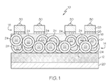
- one embodiment of the disclosed photodiode may include a substrate layer 12, a quantum nanomaterial layer 14 and a thin-film oxide layer 16.
- a first contact layer 18 may be applied over the thin-film oxide layer 16.
- a second contact layer 20 may be applied over the substrate layer 12.
- the substrate layer 12 may provide the surface upon which the quantum nanomaterial layer 14 may be deposited.
- various materials may be used to form the substrate layer 12 without departing from the scope of the present disclosure.
- the substrate layer 12 may be formed from a semiconductor material.
- the substrate layer 12 may be formed from germanium, such as germanium that starts as p-type germanium or germanium that has been doped p-type germanium.
- germanium such as germanium that starts as p-type germanium or germanium that has been doped p-type germanium.
- various semiconductor substrate materials may be used to form the substrate layer 12, and the semiconductor substrate materials may optionally be doped to achieve the desired electrical properties.
- the semiconductor substrate material e.g., germanium
- S-passivation sulfur passivation
- various sulfur passivation techniques may be used, one suitable example includes aqueous (NH 4 ) 2 S treatment, as described in greater detail in Thathachary A.V. et al., "Fermi Level Depinning at the Germanium Schottky Interface Through Sulfur Passivation," Appl. Phy. Lett. 96, 152108 (2010 ), the entire contents of which are incorporated herein by reference.
- sulfur passivation of the semiconductor substrate material may de-pin the Fermi level at the surface of the semiconductor substrate material to make repeatable ohmic contacts to the semiconductor substrate.
- the substrate layer 12 may be formed from a non-semiconductor material.
- a non-semiconductor material such conductive materials, non-conductive materials, flexible materials and rigid materials, are contemplated.
- the non-semiconductor materials may be coated with various materials, such as conductors and/or insulators, to achieve the desired electrical properties.
- the substrate layer 12 may include a conductive, flexible foil, such as a metal foil.
- the conductive, flexible foil may be coated with a thin layer (e.g., 25 nanometers or less) of insulator.
- the insulator may be applied using a solution process, such as solution-processed aluminophosphate or solution-processed hafnium oxysulfate.
- the insulator may be applied using a physical vapor deposition process.
- the insulator may allow carriers to tunnel through to the underlying conductive, flexible foil, but may preclude direct contact between the quantum nanomaterial layer 14 and the conductive, flexible foil, which may quench the desired properties of the quantum nanomaterials in the quantum nanomaterial layer 14.
- the substrate layer 12 may include a non-conductive polymeric film, such as polyetheretherketone.
- the non-conductive polymeric film may be coated with a thin, highly conductive layer.
- the thin, highly conductive layer may be a thin metal (e.g., silver) layer applied using a physical vapor deposition process.
- the thin, highly conductive layer may be coated with a thin layer (e.g., 25 nanometers or less) of insulator, such as by using a solution process or a physical vapor deposition process, as described above.
- the quantum nanomaterial layer 14 may include a plurality of quantum nanomaterials 22 applied onto a surface 13 of the substrate layer 12 as a thin film using a solution deposition technique.
- suitable solution deposition techniques include spin coating, stamping and printing.
- the quantum nanomaterials 22 may be quantum dots, quantum rods, nano-tetrapods or any other nanocrystalline semiconductor material.
- the quantum nanomaterials 22 may be tin-telluride (SnTe) quantum dots.
- the quantum nanomaterials 22 may be lead-tin-telluride (Pb (1-x) Sn x Te, where x is a number between 0.1 and 0.6) quantum dots.
- the quantum nanomaterials 22 may be tuned to absorb infrared radiation, such as infrared radiation within the bandwidth of mid-wavelength infrared (3-5 micrometers) and long-wavelength infrared (5-15 micrometers). Tuning the quantum nanomaterials 22 to absorb infrared radiation within the mid-wavelength and long-wavelength infrared spectrum may require specific material selection (e.g., forming the quantum nanomaterials 22 from tin-telluride or lead-tin-telluride) and growing the quantum nanomaterials 22 to a particular size, as described in greater detail in U.S. Patent App. No.
- the quantum nanomaterials 22 may be formed from tin-telluride (SnTe) and may have a maximum cross-sectional dimensions of between about 15 and about 50 nanometers.
- the quantum nanomaterials 22 may be formed from lead-tin-telluride (Pb x Sn (1-x) Te, where x is a number between 0.1 and 0.6) and may have a maximum cross-sectional dimensions of at least about 7.5 nanometers.
- the quantum nanomaterials 22 may include a ligand coating 24.
- the ligand coating 24 may include an inorganic ligand or a combination of inorganic ligands.
- organic ligands is also contemplated. Without being limited to any particular theory, it is believed that the ligand coating 24 may bind-up bonds on the surface of the quantum nanomaterials 22, and may allow closer spacing between adjacent quantum nanomaterials 22 within the quantum nanomaterial layer 14.
- the ligand coating 24 may include a metal chalcogenide complex ("MCC").
- MCC metal chalcogenide complex
- the metal chalcogenide complex may include a metal and a chalcogen, such as sulfur, selenium or tellurium, wherein the metal includes either tin and/or a transition metal.
- metal chalcogenide complexes suitable for use as the ligand coating 24 include tin-sulfide (SnS), tin-selenide (SnSe) and tin-telluride SnTe.
- the ligand coating 24 may include a metal halide ligand.
- the halide may be iodide, bromide and/or chloride.
- An example of a metal halide ligand suitable for use as the ligand coating 24 is titanium chloride (TiO 4 ).
- the ligand coating 24 may be applied to the quantum nanomaterials 22 using a ligand exchange process.
- the process of manufacturing quantum nanomaterials 22 may result in quantum nanomaterials 22 having a coating (e.g., oleic acid) already on the surface thereof.
- the ligand exchange process may substitute the original coating (e.g., oleic acid) for the desired ligand coating 24 (e.g., SnS, SnSe or SnTe).
- a dispersion of quantum nanomaterials 22 having a ligand coating 24 suitable for forming the quantum nanomaterial layer 14 may be prepared as follows. First, tin-telluride (SnTe) nanocrystals may be manufactured as described in U.S. Patent App. No. 13/022,705 . The manufacturing process may be controlled such that the resulting tin-telluride nanocrystals are tuned to the desired wavelength (e.g., long-wavelength infrared). The tin-telluride nanocrystals may have an oleic acid coating, and may be dispersed in hexane.
- SnTe tin-telluride
- a ligand exchange reaction may be performed to coat the tin-telluride nanocrystals with a tin-sulfide (SnS) metal chalcogenide complex.
- SnS tin-sulfide
- the SnS-coated tin-telluride nanocrystals may be dispersed in hydrazine.
- the dispersion of SnS-coated tin-telluride nanocrystals in hydrazine may be solution deposited onto the substrate layer 14, such as by spin coating, stamping or printing.
- the solution deposition process e.g., spin coating
- the solution deposition process may continue until the desired cross-sectional thickness of the quantum nanomaterial layer 14 is achieved.
- the resulting layered structure may be heat-treated (e.g., 60 minutes at 280 °C).
- the thin-film oxide layer 16 may be applied over the quantum nanomaterial layer 14, and may optionally infiltrate the quantum nanomaterial layer 14.
- the thin-film oxide layer 16 may be electrically conductive, and may be generally transparent to the electromagnetic radiation intended to be absorbed by the quantum nanomaterial layer 14.
- the thin-film oxide layer 16 may be formed from an amorphous oxide semiconductor. Those skilled in the art will appreciate that various amorphous oxide semiconductors may be used to form the thin-film oxide layer 16. Two specific examples of amorphous oxide semiconductors suitable for forming the thin-film oxide layer 16 are zinc-tin-oxide (ZTO) and indium-gallium-zinc-oxide (IGZO).
- ZTO zinc-tin-oxide
- IGZO indium-gallium-zinc-oxide
- the thin-film oxide layer 16 may be formed using a solution deposition process.
- the thin-film oxide layer 16 may be formed by synthesizing indium-gallium-zinc-oxide (IGZO) using a solution deposition process.
- IGZO indium-gallium-zinc-oxide
- a suitable IGZO solution was obtained from Inpria Corporation of Corvallis, Oregon.
- the resulting solution deposited thin-film oxide layer 16 may be heat treated for 60 minutes at 300 °C.
- the thin-film oxide layer 16 may be formed using a physical vapor deposition process.
- the thin-film oxide layer 16 may be formed from zinc-tin-oxide (ZTO) using vacuum deposition.
- the quantum nanomaterial layer 14 may be positioned between the substrate layer 12 and the thin-film oxide layer 16. Additional layers may be incorporated into the photodiode 10 without departing from the scope of the present disclosure.
- the first contact layer 18 may be applied over the thin-film oxide layer 16 and may be electrically coupled to the thin-film oxide layer 16.
- the first contact layer 18 may be formed from a conductive metal 28, such as gold, platinum, nickel, aluminum and/or tantalum.
- An optional tie layer 26, such as titanium, may be positioned between the conductive metal 28 of the first contact layer 18 and the thin-film oxide layer 16 to enhance bonding between the conductive metal 28 and the underlying thin-film oxide layer 16.
- the first contact layer 18 may be applied to the thin-film oxide layer 16 in various patterns (e.g., a grid pattern) using various techniques. As one example, the first contact layer 18 may be applied using a stamping process. As another example, the first contact layer 18 may be applied using a physical vapor deposition process (evaporation or sputtering), wherein lithography may be used to define the pattern of the first contact layer 18.
- a stamping process As another example, the first contact layer 18 may be applied using a physical vapor deposition process (evaporation or sputtering), wherein lithography may be used to define the pattern of the first contact layer 18.
- indium bumps 30 may be applied to (e.g., evaporated onto) the first contact layer 18.
- the second contact layer 20 may optionally be applied over the substrate layer 12 and may be electrically coupled to the substrate layer 12.
- the second contact layer 20 may be formed from a conductive metal, such as gold, platinum, nickel, aluminum and/or tantalum.
- one embodiment of the disclosed method for manufacturing a photodiode may begin at Block 102 with the step of providing a substrate.
- the substrate provide at Block 102 may be germanium.
- the substrate may be treated.
- the substrate may be doped.
- the germanium substrate may be doped with p-type dopants to achieve a charge carrier density of about 10 13 .
- the substrate may be subjected to sulfur passivation.
- the p-doped germanium substrate may be passivated in a (NH 4 ) 2 S solution for 30 minutes with a resistivity of 24.5 to 27.5 ohms/sq.
- the substrate may be: (1) cleaned in an HCL/HBr solution for five minutes; (2) rinsed with de-ionized water for 5 minutes and blown dry with N 2 ; (3) treated with a 40% aqueous ammonium sulfide solution at 50 °C for 5 minutes; then (4) rinsed with de-ionized water for 5 minutes and blown dry with N 2 .
- the bottom contacts may be applied to the substrate.
- the bottom contacts may be applied as follows: (1) lithography may be performed on the germanium substrate; (2) a metal, such as gold, platinum, nickel, aluminum and/or tantalum, may be applied (e.g., sputtered) over the lithography; and (3) the lithography may be lifted-off to define the bottom contacts.
- a metal such as gold, platinum, nickel, aluminum and/or tantalum
- the lithography may be lifted-off to define the bottom contacts.
- AMD may be performed, followed by a di-ionized water rinse for 5 minutes, followed by ozone treatment for 10 to 30 minutes.
- a quantum nanomaterial layer may be applied to the substrate using a solution deposition technique, such as spin coating, stamping or printing.
- a solution deposition technique such as spin coating, stamping or printing.
- the dispersion of SnS-coated tin-telluride nanocrystals in hydrazine may be applied to the germanium substrate by spin coating to achieve the desired thickness.
- the SnS-coated tin-telluride nanocrystal layer (on the germanium substrate) may be heat treated for 60 minutes at 280 °C, as shown at Block 110.
- a thin-film oxide layer may be applied over the quantum nanomaterial layer.
- an indium-gallium-zinc-oxide (IGZO) solution available from Inpria Corporation of Corvallis, Oregon, may be applied to the SnS-coated tin-telluride nanocrystal layer by spin coating to achieve the desired thickness (e.g., a single layer about 20 to 25 nanometers thick).
- the IGZO thin-film oxide layer (on the quantum nanomaterial layer, which is on the germanium substrate) may be heat treated for 60 minutes at 300 °C, as shown at Block 114.
- the thin-film oxide layer e.g., zinc-tin-oxide
- PVD physical vapor deposition
- PIC poly inorganic condensation
- an ozone treatment step may be performed following formation of the thin-film oxide layer (e.g., after Block 114).
- the top contacts may be applied to the thin-film oxide layer.
- the top contacts may be applied as follows: (1) photolithography may be performed on the thin-film oxide layer to define the top contacts; (2) a metal, such as gold with an optional titanium tie layer, may be applied (e.g., sputtered) over the photolithography; and (3) the photolithography may be lifted-off to define the top contacts.
- an indium bumps application step may be performed following formation of the top contacts (e.g., after Block 116).
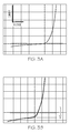
- Figs 3A and 3B show the current-voltage characteristics of a photodiode manufactured in accordance with the disclosed method 100 on a sulfur passivated, p-type doped germanium substrate having a solution cast SnS-coated SnTe nanocrystal layer and a solution cast IGZO thin-film oxide layer.
- Fig. 3A shows the current-voltage characteristics of the photodiode prior to being illuminated and
- Fig. 3B shows the current-voltage characteristics of the photodiode during illumination.
- the disclosed photodiodes may be manufacture using low-cost solution deposition processes.
- the solution deposition processes may facilitate scalable, large area (greater than 1 ft 2 ) fabrication of photodiodes on flat, as well as on curved, surfaces.
- careful selection of nanocrystal composition and size may facilitate tuning photodiodes to desired wavelength ranges (e.g., long-wavelength infrared).
Landscapes
- Light Receiving Elements (AREA)
- Photovoltaic Devices (AREA)
- Life Sciences & Earth Sciences (AREA)
- Engineering & Computer Science (AREA)
- Sustainable Development (AREA)
- Sustainable Energy (AREA)
Abstract
Description
- This application relates to photovoltaic devices and, more particularly, to photodiodes formed with quantum nanomaterials and, even more particularly, to photodiodes formed with quantum nanomaterials using solution processing techniques.
- Photodiodes convert the sun's energy into useful electrical energy (current or voltage) by way of the photovoltaic effect. Modem photodiodes are relatively lightweight and they operate at relatively high efficiencies. Therefore, photodiodes provide a reliable, lightweight and sustainable source of electrical energy suitable for a variety of applications, including terrestrial and space applications.
- Photodiodes are typically fabricated using vacuum deposition techniques to grow thin layers of semiconductor material on a substrate. The resulting photodiodes may then be electrically interconnected in large arrays to harvest the sun's energy and produce useful electrical energy.
- Unfortunately, vacuum deposition techniques generally require a substrate having a relatively small surface area (less than 1 ft2) for proper growth and, therefore, are not suitable for large surface area applications. Furthermore, vacuum deposition techniques are generally not suitable for curved surfaces and, therefore, are limited to relatively small, flat substrates. Still furthermore, vacuum deposition techniques are relatively expensive and, therefore, significantly contribute to the overall cost of photodiodes.
- Accordingly, those skilled in the art continue with research and development efforts in the field of lightweight, high efficiency photodiodes, including the fabrication of lightweight, high efficiency photodiodes.
- In one aspect, a method is provided for manufacturing a photodiode. The method may include the steps of (1) providing a substrate, (2) solution depositing (e.g., spin coating) a quantum nanomaterial layer onto the substrate, the quantum nanomaterial layer including quantum nanomaterials having a ligand coating, and (3) applying a thin-film oxide layer over the quantum nanomaterial layer.
- Optionally, the substrate includes a semiconductor material. In one embodiment, the semiconductor material includes germanium. Preferably the germanium is doped p-type germanium.
- Optionally, the method may further include the step of sulfur passivating said substrate prior to said solution depositing step.
- In some optional embodiments, the substrate comprises at least one of a metal foil and a polymeric film.
- Optionally, the plurality of quantum nanomaterials may comprise tin-telluride. Alternatively, the plurality of quantum nanomaterials comprise lead-tin-telluride.
- Optionally, the plurality of quantum nanomaterials may be a plurality of quantum dots. Each quantum dot of said plurality of quantum dots may comprise, for example, at least one of tin-telluride and/or lead-tin-telluride.
- It will be appreciated by a skilled person that each of the plurality of quantum nanomaterials can be characterized in terms of its cross-sectional dimensions, of which it will be possible to identify a 'maximum cross-sectional dimension'. The plurality of quantum nanomaterials may have substantially the same maximum cross-sectional dimension, or those dimensions may differ amongst the plurality. Preferably, the plurality of quantum nanomaterials have maximum cross-sectional dimensions of at least about 7.5 nanometers. More preferably, the plurality of quantum nanomaterials have maximum cross-sectional dimensions between about 15 nanometers and about 50 nanometers.
- In particular embodiment, the plurality of quantum nanomaterials comprises tin-telluride and the plurality of quantum nanomaterials have maximum cross-sectional dimensions between about 15 nanometers and about 50 nanometers.
- In another particular embodiment, the plurality of quantum nanomaterials comprise lead-tin-telluride and the plurality of quantum nanomaterials have maximum cross-sectional dimensions of at least about 7.5 nanometers.
- Optionally, the ligand coating comprises a metal chalcogenide complex, wherein said metal chalcogenide complex comprises at least one of tin and a transition metal. Optionally, the ligand coating may comprises at least one of tin-sulfide, tin-selenide and tin-telluride. Optionally, the ligand coating may comprise a metal halide ligand.
- In some embodiment, the thin-film oxide layer may be applied by a solution deposition process.
- Optionally, the thin-film oxide layer may comprise an amorphous oxide semiconductor.
- Optionally, the method may further include the step of applying a first contact layer over said thin-film oxide layer. Optionally, the method may further include the step of applying a second contact layer onto said substrate.
- In another aspect, a method is provided including the steps of (1) providing a substrate, (2) solution depositing (e.g., spin coating) a quantum nanomaterial layer onto the substrate, the quantum nanomaterial layer including quantum nanomaterials having a ligand coating, and (3) solution depositing (e.g., spin coating) a thin-film oxide layer over the quantum nanomaterial layer.
- In another aspect, a method is provided including the steps of (1) providing a substrate, (2) forming bottom contacts on the substrate, (3) solution depositing (e.g., spin coating) a quantum nanomaterial layer onto the substrate, the quantum nanomaterial layer including quantum nanomaterials (e.g., tin-telluride and/or lead-tin-telluride) having a ligand coating (e.g., a metal halide ligand and/or a metal chalcogenide complex), (4) applying a thin-film oxide layer over the quantum nanomaterial layer, and (5) forming top contacts on the thin-film oxide layer.
- In another aspect, a photodiode is provided including (1) a substrate, (2) a solution-cast quantum nanomaterial layer positioned on the substrate, the solution-cast quantum nanomaterial layer including tin-telluride quantum nanomaterials having a ligand coating, wherein the ligand coating includes a metal halide ligand and/or a metal chalcogenide complex, wherein the metal chalcogenide complex includes tin and/or a transition metal, and (3) a thin-film oxide layer over the solution-cast quantum nanomaterial layer.
- In yet another aspect, a photodiode is provided including (1) a substrate, (2) a solution-cast quantum nanomaterial layer positioned on the substrate, the solution-cast quantum nanomaterial layer including lead-tin-telluride quantum nanomaterials having a ligand coating, wherein the ligand coating includes a metal halide ligand and/or a metal chalcogenide complex, wherein the metal chalcogenide complex includes tin and/or a transition metal, and (3) a thin-film oxide layer over the solution-cast quantum nanomaterial layer.
- Other embodiments of the disclosed photodiodes and methods for making the same will become apparent from the following detailed description, the accompanying drawings and the appended claims.
-
-
Fig. 1 is a schematic side elevational view, in section, of one embodiment of the disclosed photodiode; -
Fig. 2 is a flow chart illustrating one embodiment of a disclosed method for making a photodiode; and -
Figs. 3A and 3B are graphical illustrations of the current-voltage characteristics of one example of the disclosed photodiode, shown prior to being illuminated (Fig. 3A ) and while being illuminated (Fig. 3B ). - It has now been discovered that photodiodes may be manufactured using solution deposition techniques, such as spin coating, stamping or printing. The disclosed solution deposition techniques may be used to manufacture photodiodes configured to operate within a particular wavelength range (e.g., long wave infrared) at a relatively lower cost than using traditional vapor deposition techniques. Furthermore, the disclosed solution deposition techniques may be used for large surface area (> 1 ft2) applications, and may be used on flat, as well as curved, surfaces.
- Referring to
Fig. 1 , one embodiment of the disclosed photodiode, generally designated 10, may include asubstrate layer 12, a quantumnanomaterial layer 14 and a thin-film oxide layer 16. Afirst contact layer 18 may be applied over the thin-film oxide layer 16. Optionally, asecond contact layer 20 may be applied over thesubstrate layer 12. - The
substrate layer 12 may provide the surface upon which thequantum nanomaterial layer 14 may be deposited. Those skilled in the art will appreciate that various materials (or combination of materials) may be used to form thesubstrate layer 12 without departing from the scope of the present disclosure. - In a first variation, the
substrate layer 12 may be formed from a semiconductor material. For example, thesubstrate layer 12 may be formed from germanium, such as germanium that starts as p-type germanium or germanium that has been doped p-type germanium. However, various semiconductor substrate materials may be used to form thesubstrate layer 12, and the semiconductor substrate materials may optionally be doped to achieve the desired electrical properties. - Optionally, the semiconductor substrate material (e.g., germanium) may be subjected to sulfur passivation (S-passivation). While various sulfur passivation techniques may be used, one suitable example includes aqueous (NH4)2S treatment, as described in greater detail in Thathachary A.V. et al., "Fermi Level Depinning at the Germanium Schottky Interface Through Sulfur Passivation," Appl. Phy. Lett. 96, 152108 (2010), the entire contents of which are incorporated herein by reference. Without being limited to any particular theory, it is believed that sulfur passivation of the semiconductor substrate material may de-pin the Fermi level at the surface of the semiconductor substrate material to make repeatable ohmic contacts to the semiconductor substrate.
- In a second variation, the
substrate layer 12 may be formed from a non-semiconductor material. Various non-semiconductor materials, such conductive materials, non-conductive materials, flexible materials and rigid materials, are contemplated. The non-semiconductor materials may be coated with various materials, such as conductors and/or insulators, to achieve the desired electrical properties. - In one expression of the second variation, the
substrate layer 12 may include a conductive, flexible foil, such as a metal foil. The conductive, flexible foil may be coated with a thin layer (e.g., 25 nanometers or less) of insulator. As one example, the insulator may be applied using a solution process, such as solution-processed aluminophosphate or solution-processed hafnium oxysulfate. As another example, the insulator may be applied using a physical vapor deposition process. Without being limited to any particular theory, it is believed that the insulator may allow carriers to tunnel through to the underlying conductive, flexible foil, but may preclude direct contact between thequantum nanomaterial layer 14 and the conductive, flexible foil, which may quench the desired properties of the quantum nanomaterials in thequantum nanomaterial layer 14. - In another expression of the second variation, the
substrate layer 12 may include a non-conductive polymeric film, such as polyetheretherketone. The non-conductive polymeric film may be coated with a thin, highly conductive layer. For example, the thin, highly conductive layer may be a thin metal (e.g., silver) layer applied using a physical vapor deposition process. Then, the thin, highly conductive layer may be coated with a thin layer (e.g., 25 nanometers or less) of insulator, such as by using a solution process or a physical vapor deposition process, as described above. - The
quantum nanomaterial layer 14 may include a plurality ofquantum nanomaterials 22 applied onto asurface 13 of thesubstrate layer 12 as a thin film using a solution deposition technique. Examples of suitable solution deposition techniques include spin coating, stamping and printing. - The quantum nanomaterials 22 may be quantum dots, quantum rods, nano-tetrapods or any other nanocrystalline semiconductor material. As one specific example, the
quantum nanomaterials 22 may be tin-telluride (SnTe) quantum dots. As another specific example, thequantum nanomaterials 22 may be lead-tin-telluride (Pb(1-x)SnxTe, where x is a number between 0.1 and 0.6) quantum dots. - The quantum nanomaterials 22 may be tuned to absorb infrared radiation, such as infrared radiation within the bandwidth of mid-wavelength infrared (3-5 micrometers) and long-wavelength infrared (5-15 micrometers). Tuning the quantum nanomaterials 22 to absorb infrared radiation within the mid-wavelength and long-wavelength infrared spectrum may require specific material selection (e.g., forming the
quantum nanomaterials 22 from tin-telluride or lead-tin-telluride) and growing thequantum nanomaterials 22 to a particular size, as described in greater detail inU.S. Patent App. No. 13/022,705 ("Nanomaterial Having Tunable Infrared Absorption Characteristics and Associated Method of Manufacture") filed on February 8, 2011, the entire contents of which are incorporated herein by reference. As one example, thequantum nanomaterials 22 may be formed from tin-telluride (SnTe) and may have a maximum cross-sectional dimensions of between about 15 and about 50 nanometers. As another example, thequantum nanomaterials 22 may be formed from lead-tin-telluride (PbxSn(1-x)Te, where x is a number between 0.1 and 0.6) and may have a maximum cross-sectional dimensions of at least about 7.5 nanometers. - The quantum nanomaterials 22 may include a
ligand coating 24. Theligand coating 24 may include an inorganic ligand or a combination of inorganic ligands. The use of organic ligands is also contemplated. Without being limited to any particular theory, it is believed that theligand coating 24 may bind-up bonds on the surface of thequantum nanomaterials 22, and may allow closer spacing between adjacentquantum nanomaterials 22 within thequantum nanomaterial layer 14. - In one formulation, the
ligand coating 24 may include a metal chalcogenide complex ("MCC"). The metal chalcogenide complex may include a metal and a chalcogen, such as sulfur, selenium or tellurium, wherein the metal includes either tin and/or a transition metal. Examples of metal chalcogenide complexes suitable for use as theligand coating 24 include tin-sulfide (SnS), tin-selenide (SnSe) and tin-telluride SnTe. - In another formulation, the
ligand coating 24 may include a metal halide ligand. For example, the halide may be iodide, bromide and/or chloride. An example of a metal halide ligand suitable for use as theligand coating 24 is titanium chloride (TiO4). - The
ligand coating 24 may be applied to thequantum nanomaterials 22 using a ligand exchange process. The process of manufacturingquantum nanomaterials 22 may result inquantum nanomaterials 22 having a coating (e.g., oleic acid) already on the surface thereof. The ligand exchange process may substitute the original coating (e.g., oleic acid) for the desired ligand coating 24 (e.g., SnS, SnSe or SnTe). - As one non-limiting example, a dispersion of
quantum nanomaterials 22 having aligand coating 24 suitable for forming thequantum nanomaterial layer 14 may be prepared as follows. First, tin-telluride (SnTe) nanocrystals may be manufactured as described inU.S. Patent App. No. 13/022,705 . The manufacturing process may be controlled such that the resulting tin-telluride nanocrystals are tuned to the desired wavelength (e.g., long-wavelength infrared). The tin-telluride nanocrystals may have an oleic acid coating, and may be dispersed in hexane. Second, a ligand exchange reaction may be performed to coat the tin-telluride nanocrystals with a tin-sulfide (SnS) metal chalcogenide complex. Finally, the SnS-coated tin-telluride nanocrystals may be dispersed in hydrazine. - To form the
quantum nanomaterial layer 14, the dispersion of SnS-coated tin-telluride nanocrystals in hydrazine may be solution deposited onto thesubstrate layer 14, such as by spin coating, stamping or printing. The solution deposition process (e.g., spin coating) may continue until the desired cross-sectional thickness of thequantum nanomaterial layer 14 is achieved. Then, after solution deposition, the resulting layered structure may be heat-treated (e.g., 60 minutes at 280 °C). - The thin-
film oxide layer 16 may be applied over thequantum nanomaterial layer 14, and may optionally infiltrate thequantum nanomaterial layer 14. The thin-film oxide layer 16 may be electrically conductive, and may be generally transparent to the electromagnetic radiation intended to be absorbed by thequantum nanomaterial layer 14. - The thin-
film oxide layer 16 may be formed from an amorphous oxide semiconductor. Those skilled in the art will appreciate that various amorphous oxide semiconductors may be used to form the thin-film oxide layer 16. Two specific examples of amorphous oxide semiconductors suitable for forming the thin-film oxide layer 16 are zinc-tin-oxide (ZTO) and indium-gallium-zinc-oxide (IGZO). - In one construction, the thin-
film oxide layer 16 may be formed using a solution deposition process. For example, the thin-film oxide layer 16 may be formed by synthesizing indium-gallium-zinc-oxide (IGZO) using a solution deposition process. A suitable IGZO solution was obtained from Inpria Corporation of Corvallis, Oregon. The resulting solution deposited thin-film oxide layer 16 may be heat treated for 60 minutes at 300 °C. - In another construction, the thin-
film oxide layer 16 may be formed using a physical vapor deposition process. For example, the thin-film oxide layer 16 may be formed from zinc-tin-oxide (ZTO) using vacuum deposition. - Thus, the
quantum nanomaterial layer 14 may be positioned between thesubstrate layer 12 and the thin-film oxide layer 16. Additional layers may be incorporated into thephotodiode 10 without departing from the scope of the present disclosure. - The
first contact layer 18 may be applied over the thin-film oxide layer 16 and may be electrically coupled to the thin-film oxide layer 16. Thefirst contact layer 18 may be formed from aconductive metal 28, such as gold, platinum, nickel, aluminum and/or tantalum. Anoptional tie layer 26, such as titanium, may be positioned between theconductive metal 28 of thefirst contact layer 18 and the thin-film oxide layer 16 to enhance bonding between theconductive metal 28 and the underlying thin-film oxide layer 16. - The
first contact layer 18 may be applied to the thin-film oxide layer 16 in various patterns (e.g., a grid pattern) using various techniques. As one example, thefirst contact layer 18 may be applied using a stamping process. As another example, thefirst contact layer 18 may be applied using a physical vapor deposition process (evaporation or sputtering), wherein lithography may be used to define the pattern of thefirst contact layer 18. - Optionally, indium bumps 30 may be applied to (e.g., evaporated onto) the
first contact layer 18. - The
second contact layer 20 may optionally be applied over thesubstrate layer 12 and may be electrically coupled to thesubstrate layer 12. Thesecond contact layer 20 may be formed from a conductive metal, such as gold, platinum, nickel, aluminum and/or tantalum. - Also disclosed is a method for manufacturing a photodiode. Referring to
Fig. 2 , one embodiment of the disclosed method for manufacturing a photodiode, generally designated 100, may begin atBlock 102 with the step of providing a substrate. For example, the substrate provide atBlock 102 may be germanium. - At
Block 104, the substrate may be treated. As one treatment, the substrate may be doped. For example, the germanium substrate may be doped with p-type dopants to achieve a charge carrier density of about 1013. As another treatment, the substrate may be subjected to sulfur passivation. For example, the p-doped germanium substrate may be passivated in a (NH4)2S solution for 30 minutes with a resistivity of 24.5 to 27.5 ohms/sq. After sulfur passivation, the substrate may be: (1) cleaned in an HCL/HBr solution for five minutes; (2) rinsed with de-ionized water for 5 minutes and blown dry with N2; (3) treated with a 40% aqueous ammonium sulfide solution at 50 °C for 5 minutes; then (4) rinsed with de-ionized water for 5 minutes and blown dry with N2. - At
Block 106, the bottom contacts may be applied to the substrate. For example, the bottom contacts may be applied as follows: (1) lithography may be performed on the germanium substrate; (2) a metal, such as gold, platinum, nickel, aluminum and/or tantalum, may be applied (e.g., sputtered) over the lithography; and (3) the lithography may be lifted-off to define the bottom contacts. Optionally, AMD may be performed, followed by a di-ionized water rinse for 5 minutes, followed by ozone treatment for 10 to 30 minutes. - At
Block 108, a quantum nanomaterial layer may be applied to the substrate using a solution deposition technique, such as spin coating, stamping or printing. For example, the dispersion of SnS-coated tin-telluride nanocrystals in hydrazine may be applied to the germanium substrate by spin coating to achieve the desired thickness. The SnS-coated tin-telluride nanocrystal layer (on the germanium substrate) may be heat treated for 60 minutes at 280 °C, as shown atBlock 110. - At
Block 112, a thin-film oxide layer may be applied over the quantum nanomaterial layer. For example, an indium-gallium-zinc-oxide (IGZO) solution available from Inpria Corporation of Corvallis, Oregon, may be applied to the SnS-coated tin-telluride nanocrystal layer by spin coating to achieve the desired thickness (e.g., a single layer about 20 to 25 nanometers thick). The IGZO thin-film oxide layer (on the quantum nanomaterial layer, which is on the germanium substrate) may be heat treated for 60 minutes at 300 °C, as shown atBlock 114. As another example, the thin-film oxide layer (e.g., zinc-tin-oxide) may be applied over the quantum nanomaterial layer using a traditional physical vapor deposition (PVD) process or poly inorganic condensation (PIC) process, which may not require an additional, post-deposition heat treatment step. - Optionally, an ozone treatment step may be performed following formation of the thin-film oxide layer (e.g., after Block 114).
- At
Block 116, the top contacts may be applied to the thin-film oxide layer. For example, the top contacts may be applied as follows: (1) photolithography may be performed on the thin-film oxide layer to define the top contacts; (2) a metal, such as gold with an optional titanium tie layer, may be applied (e.g., sputtered) over the photolithography; and (3) the photolithography may be lifted-off to define the top contacts. - Optionally, an indium bumps application step may be performed following formation of the top contacts (e.g., after Block 116).
-
Figs 3A and 3B show the current-voltage characteristics of a photodiode manufactured in accordance with the disclosedmethod 100 on a sulfur passivated, p-type doped germanium substrate having a solution cast SnS-coated SnTe nanocrystal layer and a solution cast IGZO thin-film oxide layer.Fig. 3A shows the current-voltage characteristics of the photodiode prior to being illuminated andFig. 3B shows the current-voltage characteristics of the photodiode during illumination. - Accordingly, the disclosed photodiodes may be manufacture using low-cost solution deposition processes. The solution deposition processes may facilitate scalable, large area (greater than 1 ft2) fabrication of photodiodes on flat, as well as on curved, surfaces. Furthermore, careful selection of nanocrystal composition and size may facilitate tuning photodiodes to desired wavelength ranges (e.g., long-wavelength infrared).
- Although various embodiments of the disclosed photodiode and method for making the same have been shown and described, modifications may occur to those skilled in the art upon reading the specification. The present application includes such modifications and is limited only by the scope of the claims.
Claims (15)
- A method for manufacturing a photodiode (10) comprising the steps of:providing a substrate;solution depositing a quantum nanomaterial layer (14) onto said substrate, said quantum nanomaterial layer (14) comprising a plurality of quantum nanomaterials (22), each quantum nanomaterial (22) of said plurality (22) comprising a ligand coating (24); andapplying a thin-film oxide layer (16) over said quantum nanomaterial layer (14).
- The method of Claim 1 wherein said substrate comprises a semiconductor material.
- The method of any of Claims 1 or 2 wherein said semiconductor material comprises germanium (12), such as doped p-type germanium.
- The method of any of Claims 1-3 further comprising the step of sulfur passivating said substrate prior to said solution depositing step.
- The method of any of Claims 1-4 wherein said substrate comprises at least one of a metal foil and a polymeric film.
- The method of any of Claims 1-5 wherein said plurality of quantum nanomaterials (14) is a plurality of quantum dots (22), and wherein each quantum dot (22) of said plurality of quantum dots (22)comprises at least one of tin-telluride and lead-tin-telluride.
- The method of any of Claims 1-6 wherein said plurality of quantum nanomaterials (14) comprise tin-telluride; wherein said plurality of quantum nanomaterials (14) have maximum cross-sectional dimensions between about 15 nanometers and about 50 nanometers.
- The method of any of Claims 1-6 wherein said plurality of quantum nanomaterials (14) comprise lead-tin-telluride; wherein said plurality of quantum nanomaterials (14) have maximum cross-sectional dimensions of at least about 7.5 nanometers.
- The method of any of Claims 1-8 wherein said ligand coating (24) comprises at least one of:i.) a metal chalcogenide complex, wherein said metal chalcogenide complex comprises at least one of tin and a transition metal; andii.) at least one of tin-sulfide, tin-selenide and tin-telluride.
- The method of any of Claims 1-8 wherein said ligand coating (24) comprises a metal halide ligand.
- The method of any of Claims 1-10 wherein said thin-film oxide layer (16) is applied by a solution deposition process.
- The method of any of Claims 1-11 wherein said thin-film oxide layer (16) comprises an amorphous oxide semiconductor.
- The method of any of Claims 1-12 further comprising the step of applying a first contact layer (18) over said thin-film oxide layer (16).
- The method of any of Claims 1-13 further comprising the step of applying a second contact layer (20) onto said substrate.
- A photodiode comprising:a substrate;a solution-cast quantum nanomaterial layer (14) positioned on said substrate, said solution-cast quantum nanomaterial layer (14) comprising tin-telluride and/or lead-tin-telluride quantum nanomaterials (22) comprising a ligand coating (24), wherein said ligand coating (24) comprises at least one of a metal halide ligand and a metal chalcogenide complex, wherein said metal chalcogenide complex comprises at least one of tin and a transition metal; anda thin-film oxide layer (16) over said solution-cast quantum nanomaterial layer (14).
Applications Claiming Priority (1)
| Application Number | Priority Date | Filing Date | Title |
|---|---|---|---|
| US13/549,905 US8962378B2 (en) | 2012-07-16 | 2012-07-16 | Photodiode and method for making the same |
Publications (3)
| Publication Number | Publication Date |
|---|---|
| EP2688109A2 true EP2688109A2 (en) | 2014-01-22 |
| EP2688109A3 EP2688109A3 (en) | 2018-01-10 |
| EP2688109B1 EP2688109B1 (en) | 2019-02-06 |
Family
ID=48578923
Family Applications (1)
| Application Number | Title | Priority Date | Filing Date |
|---|---|---|---|
| EP13171705.0A Active EP2688109B1 (en) | 2012-07-16 | 2013-06-12 | Photodiode and method for manufacturing the same |
Country Status (6)
| Country | Link |
|---|---|
| US (2) | US8962378B2 (en) |
| EP (1) | EP2688109B1 (en) |
| JP (1) | JP6289827B2 (en) |
| KR (1) | KR102130286B1 (en) |
| CN (1) | CN103545396B (en) |
| CA (2) | CA2815482C (en) |
Families Citing this family (8)
| Publication number | Priority date | Publication date | Assignee | Title |
|---|---|---|---|---|
| US20140079912A1 (en) * | 2012-09-17 | 2014-03-20 | The Boeing Company | Ir absorbing coatings comprisiing fluorinated nanoparticles |
| US20140315331A1 (en) * | 2013-03-13 | 2014-10-23 | Intermolecular, Inc. | Screening of Surface Passivation Processes for Germanium Channels |
| KR102672449B1 (en) * | 2016-09-19 | 2024-06-05 | 엘지디스플레이 주식회사 | Inorganic emitting particle, Inorganic emitting particle film, and LED package and Display device including the same |
| EP3399344B1 (en) | 2017-05-03 | 2021-06-30 | ams International AG | Semiconductor device for indirect detection of electromagnetic radiation and method of production |
| WO2019150987A1 (en) * | 2018-01-31 | 2019-08-08 | ソニー株式会社 | Photoelectric conversion element and imaging device |
| JPWO2021002106A1 (en) * | 2019-07-01 | 2021-01-07 | ||
| IL273118B (en) | 2020-03-05 | 2022-03-01 | Allen Richter | Self-adaptive electromagnetic energy attenuator |
| CN111976039B (en) * | 2020-08-20 | 2022-03-29 | 苏州安洁科技股份有限公司 | A kind of nano-wafer knife punching method without loss inductance |
Family Cites Families (28)
| Publication number | Priority date | Publication date | Assignee | Title |
|---|---|---|---|---|
| US3911469A (en) * | 1974-02-25 | 1975-10-07 | Texas Instruments Inc | Method of forming P-N junction in PbSnTe and photovoltaic infrared detector provided thereby |
| IL138471A0 (en) * | 2000-09-14 | 2001-10-31 | Yissum Res Dev Co | Novel semiconductor materials and their uses |
| US6696700B2 (en) * | 2001-03-09 | 2004-02-24 | National University Of Singapore | P-type transparent copper-aluminum-oxide semiconductor |
| JP2005502051A (en) * | 2001-08-28 | 2005-01-20 | アイエスピー インヴェストメンツ インコーポレイテッド | Stable radiochromic dosimetry film and manufacturing method thereof |
| CN100490205C (en) | 2003-07-10 | 2009-05-20 | 国际商业机器公司 | Method for depositing metal sulfur family film and method for preparing field effect transistor |
| US7306823B2 (en) * | 2004-09-18 | 2007-12-11 | Nanosolar, Inc. | Coated nanoparticles and quantum dots for solution-based fabrication of photovoltaic cells |
| US7742322B2 (en) * | 2005-01-07 | 2010-06-22 | Invisage Technologies, Inc. | Electronic and optoelectronic devices with quantum dot films |
| US7773404B2 (en) * | 2005-01-07 | 2010-08-10 | Invisage Technologies, Inc. | Quantum dot optical devices with enhanced gain and sensitivity and methods of making same |
| WO2006110919A2 (en) * | 2005-04-13 | 2006-10-19 | The Regents Of The University Of California | Carrier multiplication in quantum-confined semiconductor materials |
| CN101283454B (en) * | 2005-08-25 | 2011-02-23 | 爱德华·萨金特 | Quantum dot optics with enhanced gain and sensitivity |
| US7517718B2 (en) | 2006-01-12 | 2009-04-14 | International Business Machines Corporation | Method for fabricating an inorganic nanocomposite |
| US7494841B2 (en) | 2006-05-12 | 2009-02-24 | International Business Machines Corporation | Solution-based deposition process for metal chalcogenides |
| US7888700B2 (en) * | 2007-03-08 | 2011-02-15 | Eastman Kodak Company | Quantum dot light emitting device |
| EP2165354B1 (en) * | 2007-06-25 | 2018-05-30 | Massachusetts Institute of Technology | Photovoltaic device including semiconductor nanocrystals |
| DE102007043077A1 (en) | 2007-09-10 | 2009-03-12 | Robert Bosch Gmbh | Sensor arrangement and method for operating a sensor arrangement |
| US20110146766A1 (en) * | 2008-02-26 | 2011-06-23 | Solar Cells Based On Quantum Dot Or Colloidal Nanocrystal Films | Solar cells based on quantum dot or colloidal nanocrystal films |
| WO2009129353A1 (en) * | 2008-04-15 | 2009-10-22 | Purdue Research Foundation | Metallized silicon substrate for indium gallium nitride light-emitting diode |
| TWI513014B (en) * | 2008-05-19 | 2015-12-11 | Tatung Co | High performance optoelectronic components |
| JP2010067801A (en) * | 2008-09-11 | 2010-03-25 | Seiko Epson Corp | Photoelectric conversion device, electronic apparatus, method for manufacturing photoelectric conversion device, and method for manufacturing electronic apparatus |
| KR101659713B1 (en) * | 2008-12-12 | 2016-09-30 | 코닌클리케 필립스 엔.브이. | A luminescent photovoltaic generator and a waveguide for use in a photovoltaic generator |
| WO2010138636A2 (en) * | 2009-05-26 | 2010-12-02 | Purdue Research Foundation | Synthesis of multinary chalcogenide nanoparticles comprising cu, zn, sn, s, and se |
| JP2011176225A (en) * | 2010-02-25 | 2011-09-08 | Seiko Epson Corp | Optical conversion device and electronic equipment including the optical converter device |
| US9382474B2 (en) * | 2010-04-06 | 2016-07-05 | The Governing Council Of The University Of Toronto | Photovoltaic devices with depleted heterojunctions and shell-passivated nanoparticles |
| CN102237202B (en) * | 2010-04-22 | 2014-07-02 | 财团法人工业技术研究院 | Quantum dot thin film solar cells |
| JP2011249579A (en) * | 2010-05-27 | 2011-12-08 | Fujifilm Corp | Solar battery and method for manufacturing the same |
| US8871175B2 (en) | 2010-10-01 | 2014-10-28 | The Boeing Company | Nanomaterial having tunable infrared absorption characteristics and associated method of manufacture |
| US8685781B2 (en) * | 2011-07-20 | 2014-04-01 | Alliance For Sustainable Energy, Llc | Secondary treatment of films of colloidal quantum dots for optoelectronics and devices produced thereby |
| US20130042906A1 (en) * | 2011-08-19 | 2013-02-21 | Ming-Way LEE | Quantum-dot sensitized solar cell |
-
2012
- 2012-07-16 US US13/549,905 patent/US8962378B2/en active Active
-
2013
- 2013-04-16 KR KR1020130041740A patent/KR102130286B1/en active Active
- 2013-05-09 CA CA2815482A patent/CA2815482C/en active Active
- 2013-05-09 CA CA3128702A patent/CA3128702C/en active Active
- 2013-06-12 EP EP13171705.0A patent/EP2688109B1/en active Active
- 2013-07-11 JP JP2013145458A patent/JP6289827B2/en active Active
- 2013-07-15 CN CN201310301655.8A patent/CN103545396B/en active Active
-
2015
- 2015-01-13 US US14/595,358 patent/US9318631B2/en active Active
Non-Patent Citations (1)
| Title |
|---|
| THATHACHARY A.V. ET AL.: "Fermi Level Depinning at the Germanium Schottky Interface Through Sulfur Passivation", APPL. PHY. LETT., vol. 96, 2010, pages 152108, XP012130809, DOI: doi:10.1063/1.3387760 |
Also Published As
| Publication number | Publication date |
|---|---|
| US9318631B2 (en) | 2016-04-19 |
| CN103545396A (en) | 2014-01-29 |
| EP2688109A3 (en) | 2018-01-10 |
| KR20140010335A (en) | 2014-01-24 |
| CA3128702C (en) | 2023-12-19 |
| CA2815482A1 (en) | 2014-01-16 |
| KR102130286B1 (en) | 2020-07-09 |
| CA3128702A1 (en) | 2014-01-16 |
| CN103545396B (en) | 2017-04-26 |
| US20150122327A1 (en) | 2015-05-07 |
| CA2815482C (en) | 2021-09-28 |
| JP2014022734A (en) | 2014-02-03 |
| JP6289827B2 (en) | 2018-03-07 |
| US8962378B2 (en) | 2015-02-24 |
| EP2688109B1 (en) | 2019-02-06 |
| US20140014902A1 (en) | 2014-01-16 |
Similar Documents
| Publication | Publication Date | Title |
|---|---|---|
| US9318631B2 (en) | Photodiode and method for making the same | |
| Li et al. | High-performance transparent ultraviolet photodetectors based on InGaZnO superlattice nanowire arrays | |
| WO2020139131A1 (en) | Mxene-modified hybrid photoconverter | |
| US8158880B1 (en) | Thin-film photovoltaic structures including semiconductor grain and oxide layers | |
| US20130174900A1 (en) | Nanowire enhanced transparent conductive oxide for thin film photovoltaic devices | |
| US8993370B2 (en) | Reverse stack structures for thin-film photovoltaic cells | |
| US10714648B2 (en) | Solar cell with graphene-silicon quantum dot hybrid structure and method of manufacturing the same | |
| CN106229382A (en) | A kind of silicon-doped gallium nitride nano belt ultraviolet light detector and preparation method thereof | |
| TW200952194A (en) | Photovoltaic devices with enhanced efficiencies using high-aspect-ratio nanostructures | |
| Jarwal et al. | Efficiency improvement of TiO 2 nanorods electron transport layer based perovskite solar cells by solvothermal etching | |
| Zhang et al. | Inorganic solar cells based on electrospun ZnO nanofibrous networks and electrodeposited Cu2O | |
| KR101971398B1 (en) | Bifacial CdS/CdTe thin film solar cell and method for the same | |
| Wang et al. | Double open-circuit voltage of three-dimensional ZnO/CdTe solar cells by a balancing depletion layer | |
| US9496446B2 (en) | Photovoltaic devices and method of making | |
| Bayhan et al. | Eects of Post Deposition Treatments on Vacuum Evaporated CdTe Thin Films and CdS= CdTe Heterojunction Devices | |
| US20150136220A1 (en) | Method for production of a photovoltaic device in substrate configuration | |
| US20130284247A1 (en) | P-n junction semiconductor device with photovoltaic properties | |
| KR20110107934A (en) | Carbon Nanotubes / Nano Transparent Solar Cells and Manufacturing Method Thereof | |
| TWI600176B (en) | Compound solar cell and light absorbing layer manufacturing method | |
| TWI538272B (en) | Photovoltaic devices and methods for producing the same | |
| BIHI et al. | Low-Cost ZnO/Perovskite Solar Cells, Fabrication, Simulation, and Performance Optimization | |
| Jarkov et al. | Conductive polymer PEDOT: PSS back contact for CdTe solar cell | |
| US8507786B1 (en) | Manufacturing method for patterning CIGS/CIS solar cells | |
| KR101949865B1 (en) | Compound semiconductor thin film solar cell and manufacturing method therof | |
| Park et al. | Electrically conductive anti‐reflecting nanostructure for chalcogenide thin‐film solar cells |
Legal Events
| Date | Code | Title | Description |
|---|---|---|---|
| PUAI | Public reference made under article 153(3) epc to a published international application that has entered the european phase |
Free format text: ORIGINAL CODE: 0009012 |
|
| AK | Designated contracting states |
Kind code of ref document: A2 Designated state(s): AL AT BE BG CH CY CZ DE DK EE ES FI FR GB GR HR HU IE IS IT LI LT LU LV MC MK MT NL NO PL PT RO RS SE SI SK SM TR |
|
| AX | Request for extension of the european patent |
Extension state: BA ME |
|
| PUAL | Search report despatched |
Free format text: ORIGINAL CODE: 0009013 |
|
| AK | Designated contracting states |
Kind code of ref document: A3 Designated state(s): AL AT BE BG CH CY CZ DE DK EE ES FI FR GB GR HR HU IE IS IT LI LT LU LV MC MK MT NL NO PL PT RO RS SE SI SK SM TR |
|
| AX | Request for extension of the european patent |
Extension state: BA ME |
|
| RIC1 | Information provided on ipc code assigned before grant |
Ipc: H01L 31/032 20060101ALI20171204BHEP Ipc: H01L 31/0352 20060101AFI20171204BHEP Ipc: H01L 31/18 20060101ALI20171204BHEP Ipc: H01L 31/072 20120101ALI20171204BHEP |
|
| STAA | Information on the status of an ep patent application or granted ep patent |
Free format text: STATUS: REQUEST FOR EXAMINATION WAS MADE |
|
| 17P | Request for examination filed |
Effective date: 20180706 |
|
| RBV | Designated contracting states (corrected) |
Designated state(s): AL AT BE BG CH CY CZ DE DK EE ES FI FR GB GR HR HU IE IS IT LI LT LU LV MC MK MT NL NO PL PT RO RS SE SI SK SM TR |
|
| GRAP | Despatch of communication of intention to grant a patent |
Free format text: ORIGINAL CODE: EPIDOSNIGR1 |
|
| STAA | Information on the status of an ep patent application or granted ep patent |
Free format text: STATUS: GRANT OF PATENT IS INTENDED |
|
| INTG | Intention to grant announced |
Effective date: 20180827 |
|
| GRAS | Grant fee paid |
Free format text: ORIGINAL CODE: EPIDOSNIGR3 |
|
| GRAA | (expected) grant |
Free format text: ORIGINAL CODE: 0009210 |
|
| STAA | Information on the status of an ep patent application or granted ep patent |
Free format text: STATUS: THE PATENT HAS BEEN GRANTED |
|
| AK | Designated contracting states |
Kind code of ref document: B1 Designated state(s): AL AT BE BG CH CY CZ DE DK EE ES FI FR GB GR HR HU IE IS IT LI LT LU LV MC MK MT NL NO PL PT RO RS SE SI SK SM TR |
|
| REG | Reference to a national code |
Ref country code: GB Ref legal event code: FG4D |
|
| REG | Reference to a national code |
Ref country code: CH Ref legal event code: EP Ref country code: AT Ref legal event code: REF Ref document number: 1095428 Country of ref document: AT Kind code of ref document: T Effective date: 20190215 |
|
| REG | Reference to a national code |
Ref country code: IE Ref legal event code: FG4D |
|
| REG | Reference to a national code |
Ref country code: DE Ref legal event code: R096 Ref document number: 602013050434 Country of ref document: DE |
|
| REG | Reference to a national code |
Ref country code: NL Ref legal event code: MP Effective date: 20190206 |
|
| REG | Reference to a national code |
Ref country code: LT Ref legal event code: MG4D |
|
| PG25 | Lapsed in a contracting state [announced via postgrant information from national office to epo] |
Ref country code: NL Free format text: LAPSE BECAUSE OF FAILURE TO SUBMIT A TRANSLATION OF THE DESCRIPTION OR TO PAY THE FEE WITHIN THE PRESCRIBED TIME-LIMIT Effective date: 20190206 Ref country code: FI Free format text: LAPSE BECAUSE OF FAILURE TO SUBMIT A TRANSLATION OF THE DESCRIPTION OR TO PAY THE FEE WITHIN THE PRESCRIBED TIME-LIMIT Effective date: 20190206 Ref country code: LT Free format text: LAPSE BECAUSE OF FAILURE TO SUBMIT A TRANSLATION OF THE DESCRIPTION OR TO PAY THE FEE WITHIN THE PRESCRIBED TIME-LIMIT Effective date: 20190206 Ref country code: SE Free format text: LAPSE BECAUSE OF FAILURE TO SUBMIT A TRANSLATION OF THE DESCRIPTION OR TO PAY THE FEE WITHIN THE PRESCRIBED TIME-LIMIT Effective date: 20190206 Ref country code: PT Free format text: LAPSE BECAUSE OF FAILURE TO SUBMIT A TRANSLATION OF THE DESCRIPTION OR TO PAY THE FEE WITHIN THE PRESCRIBED TIME-LIMIT Effective date: 20190606 Ref country code: NO Free format text: LAPSE BECAUSE OF FAILURE TO SUBMIT A TRANSLATION OF THE DESCRIPTION OR TO PAY THE FEE WITHIN THE PRESCRIBED TIME-LIMIT Effective date: 20190506 |
|
| REG | Reference to a national code |
Ref country code: AT Ref legal event code: MK05 Ref document number: 1095428 Country of ref document: AT Kind code of ref document: T Effective date: 20190206 |
|
| PG25 | Lapsed in a contracting state [announced via postgrant information from national office to epo] |
Ref country code: GR Free format text: LAPSE BECAUSE OF FAILURE TO SUBMIT A TRANSLATION OF THE DESCRIPTION OR TO PAY THE FEE WITHIN THE PRESCRIBED TIME-LIMIT Effective date: 20190507 Ref country code: BG Free format text: LAPSE BECAUSE OF FAILURE TO SUBMIT A TRANSLATION OF THE DESCRIPTION OR TO PAY THE FEE WITHIN THE PRESCRIBED TIME-LIMIT Effective date: 20190506 Ref country code: HR Free format text: LAPSE BECAUSE OF FAILURE TO SUBMIT A TRANSLATION OF THE DESCRIPTION OR TO PAY THE FEE WITHIN THE PRESCRIBED TIME-LIMIT Effective date: 20190206 Ref country code: RS Free format text: LAPSE BECAUSE OF FAILURE TO SUBMIT A TRANSLATION OF THE DESCRIPTION OR TO PAY THE FEE WITHIN THE PRESCRIBED TIME-LIMIT Effective date: 20190206 Ref country code: LV Free format text: LAPSE BECAUSE OF FAILURE TO SUBMIT A TRANSLATION OF THE DESCRIPTION OR TO PAY THE FEE WITHIN THE PRESCRIBED TIME-LIMIT Effective date: 20190206 Ref country code: IS Free format text: LAPSE BECAUSE OF FAILURE TO SUBMIT A TRANSLATION OF THE DESCRIPTION OR TO PAY THE FEE WITHIN THE PRESCRIBED TIME-LIMIT Effective date: 20190606 |
|
| PG25 | Lapsed in a contracting state [announced via postgrant information from national office to epo] |
Ref country code: CZ Free format text: LAPSE BECAUSE OF FAILURE TO SUBMIT A TRANSLATION OF THE DESCRIPTION OR TO PAY THE FEE WITHIN THE PRESCRIBED TIME-LIMIT Effective date: 20190206 Ref country code: RO Free format text: LAPSE BECAUSE OF FAILURE TO SUBMIT A TRANSLATION OF THE DESCRIPTION OR TO PAY THE FEE WITHIN THE PRESCRIBED TIME-LIMIT Effective date: 20190206 Ref country code: SK Free format text: LAPSE BECAUSE OF FAILURE TO SUBMIT A TRANSLATION OF THE DESCRIPTION OR TO PAY THE FEE WITHIN THE PRESCRIBED TIME-LIMIT Effective date: 20190206 Ref country code: ES Free format text: LAPSE BECAUSE OF FAILURE TO SUBMIT A TRANSLATION OF THE DESCRIPTION OR TO PAY THE FEE WITHIN THE PRESCRIBED TIME-LIMIT Effective date: 20190206 Ref country code: AL Free format text: LAPSE BECAUSE OF FAILURE TO SUBMIT A TRANSLATION OF THE DESCRIPTION OR TO PAY THE FEE WITHIN THE PRESCRIBED TIME-LIMIT Effective date: 20190206 Ref country code: EE Free format text: LAPSE BECAUSE OF FAILURE TO SUBMIT A TRANSLATION OF THE DESCRIPTION OR TO PAY THE FEE WITHIN THE PRESCRIBED TIME-LIMIT Effective date: 20190206 Ref country code: DK Free format text: LAPSE BECAUSE OF FAILURE TO SUBMIT A TRANSLATION OF THE DESCRIPTION OR TO PAY THE FEE WITHIN THE PRESCRIBED TIME-LIMIT Effective date: 20190206 Ref country code: IT Free format text: LAPSE BECAUSE OF FAILURE TO SUBMIT A TRANSLATION OF THE DESCRIPTION OR TO PAY THE FEE WITHIN THE PRESCRIBED TIME-LIMIT Effective date: 20190206 |
|
| REG | Reference to a national code |
Ref country code: DE Ref legal event code: R097 Ref document number: 602013050434 Country of ref document: DE |
|
| PG25 | Lapsed in a contracting state [announced via postgrant information from national office to epo] |
Ref country code: SM Free format text: LAPSE BECAUSE OF FAILURE TO SUBMIT A TRANSLATION OF THE DESCRIPTION OR TO PAY THE FEE WITHIN THE PRESCRIBED TIME-LIMIT Effective date: 20190206 Ref country code: PL Free format text: LAPSE BECAUSE OF FAILURE TO SUBMIT A TRANSLATION OF THE DESCRIPTION OR TO PAY THE FEE WITHIN THE PRESCRIBED TIME-LIMIT Effective date: 20190206 |
|
| PLBE | No opposition filed within time limit |
Free format text: ORIGINAL CODE: 0009261 |
|
| STAA | Information on the status of an ep patent application or granted ep patent |
Free format text: STATUS: NO OPPOSITION FILED WITHIN TIME LIMIT |
|
| PG25 | Lapsed in a contracting state [announced via postgrant information from national office to epo] |
Ref country code: AT Free format text: LAPSE BECAUSE OF FAILURE TO SUBMIT A TRANSLATION OF THE DESCRIPTION OR TO PAY THE FEE WITHIN THE PRESCRIBED TIME-LIMIT Effective date: 20190206 |
|
| REG | Reference to a national code |
Ref country code: DE Ref legal event code: R082 Ref document number: 602013050434 Country of ref document: DE Representative=s name: MAIER, LL.M., MICHAEL C., DE Ref country code: DE Ref legal event code: R082 Ref document number: 602013050434 Country of ref document: DE Representative=s name: BOULT WADE TENNANT LLP, DE |
|
| 26N | No opposition filed |
Effective date: 20191107 |
|
| PG25 | Lapsed in a contracting state [announced via postgrant information from national office to epo] |
Ref country code: MC Free format text: LAPSE BECAUSE OF FAILURE TO SUBMIT A TRANSLATION OF THE DESCRIPTION OR TO PAY THE FEE WITHIN THE PRESCRIBED TIME-LIMIT Effective date: 20190206 |
|
| REG | Reference to a national code |
Ref country code: CH Ref legal event code: PL |
|
| REG | Reference to a national code |
Ref country code: DE Ref legal event code: R082 Ref document number: 602013050434 Country of ref document: DE Representative=s name: BOULT WADE TENNANT LLP, DE |
|
| PG25 | Lapsed in a contracting state [announced via postgrant information from national office to epo] |
Ref country code: SI Free format text: LAPSE BECAUSE OF FAILURE TO SUBMIT A TRANSLATION OF THE DESCRIPTION OR TO PAY THE FEE WITHIN THE PRESCRIBED TIME-LIMIT Effective date: 20190206 |
|
| REG | Reference to a national code |
Ref country code: BE Ref legal event code: MM Effective date: 20190630 |
|
| PG25 | Lapsed in a contracting state [announced via postgrant information from national office to epo] |
Ref country code: TR Free format text: LAPSE BECAUSE OF FAILURE TO SUBMIT A TRANSLATION OF THE DESCRIPTION OR TO PAY THE FEE WITHIN THE PRESCRIBED TIME-LIMIT Effective date: 20190206 |
|
| PG25 | Lapsed in a contracting state [announced via postgrant information from national office to epo] |
Ref country code: IE Free format text: LAPSE BECAUSE OF NON-PAYMENT OF DUE FEES Effective date: 20190612 |
|
| PG25 | Lapsed in a contracting state [announced via postgrant information from national office to epo] |
Ref country code: LI Free format text: LAPSE BECAUSE OF NON-PAYMENT OF DUE FEES Effective date: 20190630 Ref country code: CH Free format text: LAPSE BECAUSE OF NON-PAYMENT OF DUE FEES Effective date: 20190630 Ref country code: LU Free format text: LAPSE BECAUSE OF NON-PAYMENT OF DUE FEES Effective date: 20190612 Ref country code: BE Free format text: LAPSE BECAUSE OF NON-PAYMENT OF DUE FEES Effective date: 20190630 |
|
| PG25 | Lapsed in a contracting state [announced via postgrant information from national office to epo] |
Ref country code: CY Free format text: LAPSE BECAUSE OF FAILURE TO SUBMIT A TRANSLATION OF THE DESCRIPTION OR TO PAY THE FEE WITHIN THE PRESCRIBED TIME-LIMIT Effective date: 20190206 |
|
| PG25 | Lapsed in a contracting state [announced via postgrant information from national office to epo] |
Ref country code: MT Free format text: LAPSE BECAUSE OF FAILURE TO SUBMIT A TRANSLATION OF THE DESCRIPTION OR TO PAY THE FEE WITHIN THE PRESCRIBED TIME-LIMIT Effective date: 20190206 Ref country code: HU Free format text: LAPSE BECAUSE OF FAILURE TO SUBMIT A TRANSLATION OF THE DESCRIPTION OR TO PAY THE FEE WITHIN THE PRESCRIBED TIME-LIMIT; INVALID AB INITIO Effective date: 20130612 |
|
| PG25 | Lapsed in a contracting state [announced via postgrant information from national office to epo] |
Ref country code: MK Free format text: LAPSE BECAUSE OF FAILURE TO SUBMIT A TRANSLATION OF THE DESCRIPTION OR TO PAY THE FEE WITHIN THE PRESCRIBED TIME-LIMIT Effective date: 20190206 |
|
| P01 | Opt-out of the competence of the unified patent court (upc) registered |
Effective date: 20230516 |
|
| REG | Reference to a national code |
Ref country code: DE Ref legal event code: R079 Ref document number: 602013050434 Country of ref document: DE Free format text: PREVIOUS MAIN CLASS: H01L0031035200 Ipc: H10F0077140000 |
|
| PGFP | Annual fee paid to national office [announced via postgrant information from national office to epo] |
Ref country code: DE Payment date: 20250627 Year of fee payment: 13 |
|
| PGFP | Annual fee paid to national office [announced via postgrant information from national office to epo] |
Ref country code: GB Payment date: 20250627 Year of fee payment: 13 |
|
| PGFP | Annual fee paid to national office [announced via postgrant information from national office to epo] |
Ref country code: FR Payment date: 20250625 Year of fee payment: 13 |