EP2688091A1 - Method for producing a cavity by anisotropically removing material from a substrate - Google Patents
Method for producing a cavity by anisotropically removing material from a substrate Download PDFInfo
- Publication number
- EP2688091A1 EP2688091A1 EP12176910.3A EP12176910A EP2688091A1 EP 2688091 A1 EP2688091 A1 EP 2688091A1 EP 12176910 A EP12176910 A EP 12176910A EP 2688091 A1 EP2688091 A1 EP 2688091A1
- Authority
- EP
- European Patent Office
- Prior art keywords
- substrate
- layer
- metal
- cavity
- alloy
- Prior art date
- Legal status (The legal status is an assumption and is not a legal conclusion. Google has not performed a legal analysis and makes no representation as to the accuracy of the status listed.)
- Granted
Links
Images


Classifications
-
- H—ELECTRICITY
- H10—SEMICONDUCTOR DEVICES; ELECTRIC SOLID-STATE DEVICES NOT OTHERWISE PROVIDED FOR
- H10P—GENERIC PROCESSES OR APPARATUS FOR THE MANUFACTURE OR TREATMENT OF DEVICES COVERED BY CLASS H10
- H10P50/00—Etching of wafers, substrates or parts of devices
-
- B—PERFORMING OPERATIONS; TRANSPORTING
- B81—MICROSTRUCTURAL TECHNOLOGY
- B81C—PROCESSES OR APPARATUS SPECIALLY ADAPTED FOR THE MANUFACTURE OR TREATMENT OF MICROSTRUCTURAL DEVICES OR SYSTEMS
- B81C99/00—Subject matter not provided for in other groups of this subclass
- B81C99/0075—Manufacture of substrate-free structures
- B81C99/009—Manufacturing the stamps or the moulds
Definitions
- the present invention is related to the anisotropic formation of cavities in a substrate surface, such as pyramid-shaped molds or V-shaped and vertical trenches.
- Anisotropic Si etching is widely used in the area of micro- and nano-electromechanical systems (MEMS, NEMS) to produce a pre-defined shape into Si by selective Si removal using an anisotropic etchant.
- Typical anisotropic etchants are potassium hydroxide (KOH), sodium hydroxide (NaOH), and tetra-methyl ammonium hydroxide (TMAH) but also many others have been demonstrated such as ethylenediamine-pyrocatechol (EDP), hydrazine, cesium hydroxide (CsOH), ammonium hydroxide (NH 4 OH) and lithium hydroxide (LiOH).
- KOH potassium hydroxide
- NaOH sodium hydroxide
- TMAH tetra-methyl ammonium hydroxide
- EDP ethylenediamine-pyrocatechol
- CsOH cesium hydroxide
- NH 4 OH ammonium hydroxide
- LiOH lithium hydroxide
- the shape which is defined into Si is depending on the orientation of the used Si wafer and the orientation of the hardmask opening.
- the typical [100]-oriented wafer gives inverted pyramids when a square (oriented parallel to the [110] direction) or a circular mask opening is used. In case of a rectangular mask opening (oriented parallel to the [110] direction), a V-shaped trench is formed.
- the etched pits are often used directly for a device, e.g. a Si membrane used as part of a pressure sensor or a trench in Si is used as a liquid channel, or they can be used as molds where the etch pit is filled up with a material such as Si 3 N 4 , metal or diamond and the Si mold is finally removed by an etching step. In this way, pyramidal tips are created for use in scanning probe microscopy (SPM).
- SPM scanning probe microscopy
- KOH and NaOH are their non-compatibility with IC processing. Elaborate cleaning procedures are required. KOH is especially problematic as it is well know that Fe-nanoparticles from the KOH pellets do deposit onto the wafer and must be cleaned afterwards by diluted HC1.
- Another disadvantage of common anisotropic etching is that it is based on wet chemistry. The wafer has to be etched in a beaker or a wetbench. Due to the release of gaseous by-products such as H 2 during the etching, the wafer should be held under an angle to let the gas bubbles escape from the etched surface (otherwise these bubbles can passivate the surface which leads to hillocks and increased roughness).
- the hardmask material is also considerably attacked during etching (e.g. for KOH the etch rate ratio between Si and SiO 2 is about 400).
- the hardmask material is often SiO 2 for small depths and Si 3 N 4 for high depths.
- SiO 2 layers can be easily etched away afterwards by HF-based chemistry without affecting the etch pit, the low-pressure chemical vapor-deposited (LPCVD) Si 3 N 4 can only be removed by 140°C hot H 3 PO 4 etching or reactive ion etching (RIE), which affects the etch pit.
- the etch rate is relatively low, for example the etch rate of 30% KOH at 70°C is about 42 ⁇ m/h. It is to be noted also that commonly fresh etching solutions are used every time for obtaining smooth etched surfaces and hence chemical consumption is considerable and expensive.
- the step of producing a metal layer on at least one selected portion of the surface is done by:
- the method of the invention further comprises the steps of:
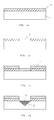
- Figure 1 illustrates the steps of one embodiment of the method of the invention for forming a cavity in the shape of an inverted pyramid.
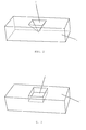
- Figure 2 shows a 3D view of a pyramidal cavity obtainable by the method of the invention.
- Figure 5 illustrates a variation of the embodiment of figure 4 , wherein the Al areas are produced in pre-formed cavities in the silicon substrate.
- the choice of the substrate material and the metal in the method is such that the dissolution rate of the substrate material into the metal depends on the crystal plane of the crystallographic structure of the substrate.
- the alloy forms in a volume that is shaped along predefined crystallographic planes, for example an inverted pyramid or V-shaped trench.
- the preferred combination of materials is silicon for the substrate and aluminium as the deposited metal. The rest of this description is based on that preferred combination Si/Al, but the description is valid also for any other suitable combination (a suitable combination being defined as a substrate material and metal such that the dissolution rate of the substrate material into the metal depends on the crystal plane of the crystallographic structure of the substrate).
- FIG. 1a illustrates a (100)Si substrate 1 provided with a hardmask 2, for example a silicon nitride or silicon oxide hardmask.
- the hardmask is locally opened by a lithography and etching step as known per se in the art ( figure 1b ), thereby forming an exposed area 3 of the Si-substrate.
- the hardmask opening has typically a square, rectangular, circular or oval shape for [100] and [110]-oriented Si wafers.
- the hardmask is removed by a suitable etch technique known as such in the art ( figure 1f ), resulting in the substrate 1 being provided with the cavity 7 (illustrated in 3D view in figure 2 ).
- the shape and size of the cavity 7 is directly related to the thickness and the shape (i.e. the shape of the hardmask opening) of the aluminium layer 4'.
- the thickness and shape of the metal layer 4' are selected specifically on the basis of a desired cavity shape and size (e.g. a V-shaped trench with given dimensions).
- the locally produced Al-layers 10 may be produced in pre-formed cavities in the substrate surface, as shown in figure 5a to 5c .
- the cavity 20 can be formed by a standard lithography and etching technique.
- the Al-layer 10 is produced also by standard lithography as in the embodiment of figure 4 .
- the same steps as described above are performed: annealing, cooling, etching to remove the alloy.
- the final cavity 30 that is formed has a pyramidal portion 31 and a portion 32 with vertical side walls.
- the pre-formed cavity 20 could be larger (as seen from above) than the pyramidal cavity 31 formed by the Al-Si alloy, thus resulting in a cavity with a larger portion with vertical side-walls and a smaller portion formed by the Al-Si alloy, for example in the middle of the larger cavity portion.
- the metal layer 4 or 10 may be an Al-based alloy, e.g. Al with boron.
Landscapes
- Engineering & Computer Science (AREA)
- Manufacturing & Machinery (AREA)
- Microelectronics & Electronic Packaging (AREA)
- Weting (AREA)
- ing And Chemical Polishing (AREA)
Abstract
Description
- The present invention is related to the anisotropic formation of cavities in a substrate surface, such as pyramid-shaped molds or V-shaped and vertical trenches.
- Anisotropic Si etching is widely used in the area of micro- and nano-electromechanical systems (MEMS, NEMS) to produce a pre-defined shape into Si by selective Si removal using an anisotropic etchant. Typical anisotropic etchants are potassium hydroxide (KOH), sodium hydroxide (NaOH), and tetra-methyl ammonium hydroxide (TMAH) but also many others have been demonstrated such as ethylenediamine-pyrocatechol (EDP), hydrazine, cesium hydroxide (CsOH), ammonium hydroxide (NH4OH) and lithium hydroxide (LiOH). The fundamental principle of anisotropic etching is that the etch rate is very different for different crystal planes. The shape which is defined into Si is depending on the orientation of the used Si wafer and the orientation of the hardmask opening. The typical [100]-oriented wafer gives inverted pyramids when a square (oriented parallel to the [110] direction) or a circular mask opening is used. In case of a rectangular mask opening (oriented parallel to the [110] direction), a V-shaped trench is formed.
- The etched pits are often used directly for a device, e.g. a Si membrane used as part of a pressure sensor or a trench in Si is used as a liquid channel, or they can be used as molds where the etch pit is filled up with a material such as Si3N4, metal or diamond and the Si mold is finally removed by an etching step. In this way, pyramidal tips are created for use in scanning probe microscopy (SPM).
- An important drawback of the most commonly used etchants KOH and NaOH is their non-compatibility with IC processing. Elaborate cleaning procedures are required. KOH is especially problematic as it is well know that Fe-nanoparticles from the KOH pellets do deposit onto the wafer and must be cleaned afterwards by diluted HC1. Another disadvantage of common anisotropic etching is that it is based on wet chemistry. The wafer has to be etched in a beaker or a wetbench. Due to the release of gaseous by-products such as H2 during the etching, the wafer should be held under an angle to let the gas bubbles escape from the etched surface (otherwise these bubbles can passivate the surface which leads to hillocks and increased roughness). Moreover, the hardmask material is also considerably attacked during etching (e.g. for KOH the etch rate ratio between Si and SiO2 is about 400). The hardmask material is often SiO2 for small depths and Si3N4 for high depths. Although SiO2 layers can be easily etched away afterwards by HF-based chemistry without affecting the etch pit, the low-pressure chemical vapor-deposited (LPCVD) Si3N4 can only be removed by 140°C hot H3PO4 etching or reactive ion etching (RIE), which affects the etch pit. Furthermore, the etch rate is relatively low, for example the etch rate of 30% KOH at 70°C is about 42 µm/h. It is to be noted also that commonly fresh etching solutions are used every time for obtaining smooth etched surfaces and hence chemical consumption is considerable and expensive.
- The invention is related to a method forming a cavity in a substrate as disclosed in the appended claims, that overcomes the problems cited above. The method of the invention comprises the steps of:
- Providing a substrate comprising at least a top layer consisting of a crystalline material,
- Determining a desired shape and size of a cavity which is to be produced in said substrate,
- Determining on the basis of said desired shape and size the thickness and shape of a layer of a metal, wherein the crystalline material's dissolution rate into said metal is not the same for each crystallographic plane of said material's crystallographic structure,
- Producing a layer of said metal, said layer having said determined thickness and shape, on and in contact with at least one selected portion of the surface of said top layer,
- Heating the substrate at a temperature suitable for causing the dissolution of said crystalline material into said metal,
- cooling the substrate, thereby forming a volume of an alloy of the metal and the crystalline material,
- Removing said volume of said alloy, thereby obtaining a cavity of said desired shape and size in said substrate.
- According to one embodiment, the step of producing a metal layer on at least one selected portion of the surface is done by:
- Producing a patterned mask layer on the surface of said top layer, thereby leaving one or more portions of said surface exposed,
- Depositing a metal layer on top of said mask layer, so that one or more portions of said metal layer are in direct contact with said one or more exposed surface portions.
- According to another embodiment, the step of producing a metal layer on at least one selected portion of the surface is done by locally depositing said metal layer on said at least one selected portion.
- According to an embodiment, said crystalline material is crystalline silicon, and said metal is aluminium or an aluminium-based alloy. An the latter case, , an interface layer may be formed during the cooling step, between said volume and the material of the substrate, said interface layer consisting of Al-doped silicon. Further in the case of the Si/Al embodiment, the step of removing the alloy volume may be done by wet etching, wherein said interface layer acts as an etch stop layer during said wet etching step.
- According to an embodiment, the method of the invention further comprises the steps of:
- Depositing a filling material at least in said cavity,
- Separating the filling material and the substrate, to thereby obtain a structure formed of said filling material and shaped by said cavity.
-
Figure 1 illustrates the steps of one embodiment of the method of the invention for forming a cavity in the shape of an inverted pyramid. -
Figure 2 shows a 3D view of a pyramidal cavity obtainable by the method of the invention. -
Figure 3 shows a 3D view of a rectangular-shaped cavity obtainable by the method of the invention. -
Figure 4 illustrates the method according to another embodiment, wherein separate areas of aluminium are produced on a silicon substrate. -
Figure 5 illustrates a variation of the embodiment offigure 4 , wherein the Al areas are produced in pre-formed cavities in the silicon substrate. - The invention is related to a method for producing cavities in a crystalline substrate or a substrate comprising a crystalline top layer, preferably a semiconductor substrate/top layer. The substrate can be a flat wafer or any other object with a surface that is suitable for performing on it the method steps of the invention. According to a preferred embodiment, a patterned hardmask is formed on the substrate, leaving one or more portions of the substrate exposed. Then a metal layer is deposited on top of the hardmask and on the exposed portions, and the substrate is heated so as to produce - in the exposed areas - an alloy of the substrate material and the added metal, through the dissolution of the substrate material into the metal. The choice of the substrate material and the metal in the method is such that the dissolution rate of the substrate material into the metal depends on the crystal plane of the crystallographic structure of the substrate. In this way, the alloy forms in a volume that is shaped along predefined crystallographic planes, for example an inverted pyramid or V-shaped trench. The preferred combination of materials is silicon for the substrate and aluminium as the deposited metal. The rest of this description is based on that preferred combination Si/Al, but the description is valid also for any other suitable combination (a suitable combination being defined as a substrate material and metal such that the dissolution rate of the substrate material into the metal depends on the crystal plane of the crystallographic structure of the substrate).
- The dissolution rate of silicon in aluminium is lowest in the Si(111) plane due to the higher packing density in that plane. In this way, a pyramidal cavity can be produced by starting from a (100)-oriented silicon wafer, as illustrated in
figure 1 .Figure 1a illustrates a (100)Si substrate 1 provided with ahardmask 2, for example a silicon nitride or silicon oxide hardmask. The hardmask is locally opened by a lithography and etching step as known per se in the art (figure 1b ), thereby forming an exposedarea 3 of the Si-substrate. The hardmask opening has typically a square, rectangular, circular or oval shape for [100] and [110]-oriented Si wafers. For Si wafers with other orientations, other preferred hardmask opening shapes may be used, e.g. triangular for [311]-oriented wafers. Then analuminium layer 4 is deposited, e.g. by sputtering or evaporation, onto the Si substrate and the hardmask, thereby forming an Al-layer 4' that is in direct contact with the exposed Si inside the hardmask opening 3 (figure 1c ). The thickness of the deposited Al-layer is preferably between 100nm and 10µm. Then the substrate is annealed, preferably to a temperature higher than or equal to 800°C. During this anneal step, silicon dissolves into the aluminium layer 4', and avolume 5 of Si-Al alloy is formed in a pyramidal shape, due to the lower dissolution rate of Si in the (111)plane (figure 1d ). - Then the substrate is cooled. During the cooling cycle, Si segregates out of the Si-Al alloy and epitaxially deposits onto the Si-to-Si/Al interface, thereby creating a highly Al-doped
Si region 6. In the next step, the Si-Al alloy can be removed by a wet etching step (figure 1e ), leaving apyramidal cavity 7. The etchant used can be an HCl containing etchant. Depending on the type of etchant used, the Al-dopedlayer 6 may act as an etch stop layer, thereby protecting the Si-substrate underneath during the wet etching step. Alternatively, the Al-doped layer is removed together with the Si-Al alloy in one etch step. The Al-doped layer could also be removed in a separate etch step. - Following this, the hardmask is removed by a suitable etch technique known as such in the art (
figure 1f ), resulting in thesubstrate 1 being provided with the cavity 7 (illustrated in 3D view infigure 2 ). The shape and size of thecavity 7 is directly related to the thickness and the shape (i.e. the shape of the hardmask opening) of the aluminium layer 4'. In the method of the invention, the thickness and shape of the metal layer 4' are selected specifically on the basis of a desired cavity shape and size (e.g. a V-shaped trench with given dimensions). - The substrate provided with the
cavity 7 may for example be used as a mold for the production of a probe tip.Figure 1g illustrates the step of filling the mold with asuitable material 8, e.g. metal, diamond, oxide or nitride. Then thesubstrate 1 may be removed, resulting in thetip structure 9, forming at least part of a MEMS/NEMS device structure (e.g. scanning probe tip, field emission tip). The Al-dopedregion 6 can either be etched away during Si mold removal or stay in place, thereby protecting the tip material from etch attack or acting as an electrically conductive layer. - The method of the invention may be used to form other shapes of cavities, by adapting the shape of the exposed
areas 3 and/or by starting from a substrate with a different crystallographic orientation. For example, instead of a pyramidal pit, a trench with vertical sidewalls may be formed starting from a (110)-oriented silicon wafer, as illustrated infigure 3 . The obtained geometry of the cavity can be directly used as part of a MEMS/NEMS device. For example, long knife-shaped grooves can be used as alignment features for optical fibers or for chip alignment. An orifice through the Si substrate may be created (by extra polishing or etching from both sides). It should be pointed out that the present invention targets also wafer crystal orientations other than the common (100)-orientation leading to pyramidal structures. Examples are (110) substrates (as illustrated infigure 3 ) and (311)-cut wafers. Other orientations might be used as well. - As stated, the thickness of the aluminium layer deposited on the exposed
Si area 3 is used to control the shape of the formed cavity. In the case offigure 1 , less aluminium may be deposited than would be required for forming an inverted pyramid with a sharp tip. The result is the formation of a truncated pyramid. By a separate patterning step, the aluminium layer 4' on the exposedarea 3 may be brought into a specific shape, which will have an additional influence on the final shape of the cavity. This is a capability that is not available in the classic anisotropic wet etching methods. - As an alternative to the embodiment of
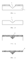
figure 1 , it is possible to produceseparate layers 10 of aluminium locally on the Si-substrate, instead of depositing a layer of aluminium over a patterned mask layer. This embodiment is illustrated infigures 4a to 4d . In this embodiment, a patternedhardmask 15 is preferably deposited on the substrate before producing theseparate layers 10 in the openings of the hardmask (Figures 4a and 4b ). Thelayer 10 can be produced by a standard lithography and etching step (deposition of Al-layer and resist layer, patterning the resist, etching Al so that Al remains only in desired areas, removing resist). On the substrate as shown infigure 4b , the same steps of annealing, cooling and etching for removal of the alloy are performed as described with respect tofigure 1 , resulting in the same type of cavity 7 (as shown infigures 4c and 4d ). In this embodiment, the hardmask 15 (although preferred in order to laterally contain the Si-Al during formation of the alloy) is not required during the formation of the cavity, which is equally a capability not available in the prior art methods, where the hardmask is necessary to protect the areas outside the zones where the cavities are to be formed. When several of such Al-layers 10 are produced separately in the manner shown infigure 4 , these layers could be deposited in different thicknesses, which provides an additional means of controlling the shape and size of the formed cavity. - In a variation of this embodiment, the locally produced Al-
layers 10 may be produced in pre-formed cavities in the substrate surface, as shown infigure 5a to 5c . Thecavity 20 can be formed by a standard lithography and etching technique. In this embodiment also, it is preferable to produce a patternedhardmask 21 on the top surface of thesubstrate 1 and on the vertical side walls of thepre-formed cavity 20, before producing the Al-layer 10 in the openings of the hardmask, i.e. at the bottom of thecavity 20. Then the Al-layer 10 is produced also by standard lithography as in the embodiment offigure 4 . Then the same steps as described above are performed: annealing, cooling, etching to remove the alloy. Thefinal cavity 30 that is formed has apyramidal portion 31 and aportion 32 with vertical side walls. Contrary to the example shown infigure 5 , thepre-formed cavity 20 could be larger (as seen from above) than thepyramidal cavity 31 formed by the Al-Si alloy, thus resulting in a cavity with a larger portion with vertical side-walls and a smaller portion formed by the Al-Si alloy, for example in the middle of the larger cavity portion. - In all of the embodiments described above, instead of pure aluminium, the
metal layer - While the invention has been illustrated and described in detail in the drawings and foregoing description, such illustration and description are to be considered illustrative or exemplary and not restrictive. Other variations to the disclosed embodiments can be understood and effected by those skilled in the art in practicing the claimed invention, from a study of the drawings, the disclosure and the appended claims. In the claims, the word "comprising" does not exclude other elements or steps, and the indefinite article "a" or "an" does not exclude a plurality. The mere fact that certain measures are recited in mutually different dependent claims does not indicate that a combination of these measures cannot be used to advantage. Any reference signs in the claims should not be construed as limiting the scope.
- The foregoing description details certain embodiments of the invention. It will be appreciated, however, that no matter how detailed the foregoing appears in text, the invention may be practiced in many ways, and is therefore not limited to the embodiments disclosed. It should be noted that the use of particular terminology when describing certain features or aspects of the invention should not be taken to imply that the terminology is being re-defined herein to be restricted to include any specific characteristics of the features or aspects of the invention with which that terminology is associated.
Claims (7)
- A method for forming a cavity in a substrate, said method comprising the steps of :- Providing a substrate (1) comprising at least a top layer consisting of a crystalline material,- Determining a desired shape and size of a cavity (7) which is to be produced in said substrate,- Determining on the basis of said desired shape and size the thickness and shape of a layer (4',10) of a metal, wherein the crystalline material's dissolution rate into said metal is not the same for each crystallographic plane of said material's crystallographic structure,- Producing a layer (4',10) of said metal, said layer having said determined thickness and shape, on and in contact with at least one selected portion (3) of the surface of said top layer,- Heating the substrate (1) at a temperature suitable for causing the dissolution of said crystalline material into said metal,- cooling the substrate, thereby forming a volume (5) of an alloy of the metal and the crystalline material,- Removing said volume of said alloy, thereby obtaining a cavity (7) of said desired shape and size in said substrate.
- The method according to claim 1, wherein the step of producing a metal layer on at least one selected portion of the surface is done by :- Producing a patterned mask layer (2) on the surface of said top layer, thereby leaving one or more portions (3) of said surface exposed,- Depositing a metal layer (4) on top of said mask layer, so that one or more portions (4') of said metal layer are in direct contact with said one or more exposed surface portions (3).
- The method according to claim 1, wherein the step of producing a metal layer on at least one selected portion (3) of the surface is done by locally depositing said metal layer (10) on said at least one selected portion.
- The method according to any one of the preceding claims, wherein said crystalline material is crystalline silicon, and wherein said metal is aluminium or an aluminium-based alloy.
- The method according to claim 4, wherein during the cooling step, an interface layer (6) is formed between said volume and the material of the substrate, said interface layer consisting of Al-doped silicon.
- The method according to claim 5, wherein the step of removing the alloy volume (5) is done by wet etching, and wherein said interface layer (6) acts as an etch stop layer during said wet etching step.
- The method according to any one of the preceding claims, further comprising the steps of :- Depositing a filling material (8) at least in said cavity (7),- Separating the filling material (8) and the substrate (1), to thereby obtain a structure (9) formed of said filling material and shaped by said cavity.
Priority Applications (1)
| Application Number | Priority Date | Filing Date | Title |
|---|---|---|---|
| EP12176910.3A EP2688091B1 (en) | 2012-07-18 | 2012-07-18 | Method for producing a cavity by anisotropically removing material from a substrate |
Applications Claiming Priority (1)
| Application Number | Priority Date | Filing Date | Title |
|---|---|---|---|
| EP12176910.3A EP2688091B1 (en) | 2012-07-18 | 2012-07-18 | Method for producing a cavity by anisotropically removing material from a substrate |
Publications (2)
| Publication Number | Publication Date |
|---|---|
| EP2688091A1 true EP2688091A1 (en) | 2014-01-22 |
| EP2688091B1 EP2688091B1 (en) | 2016-03-16 |
Family
ID=46754282
Family Applications (1)
| Application Number | Title | Priority Date | Filing Date |
|---|---|---|---|
| EP12176910.3A Not-in-force EP2688091B1 (en) | 2012-07-18 | 2012-07-18 | Method for producing a cavity by anisotropically removing material from a substrate |
Country Status (1)
| Country | Link |
|---|---|
| EP (1) | EP2688091B1 (en) |
Citations (4)
| Publication number | Priority date | Publication date | Assignee | Title |
|---|---|---|---|---|
| GB939841A (en) * | 1958-12-24 | 1963-10-16 | Pye Ltd | Method of producing junction regions in semiconductor materials |
| US5366925A (en) * | 1993-09-27 | 1994-11-22 | United Microelectronics Corporation | Local oxidation of silicon by using aluminum spiking technology |
| EP0763844A1 (en) * | 1995-09-14 | 1997-03-19 | Canon Kabushiki Kaisha | Method of manufacturing micro-tip and female mold substrate therefor, and method of manufacturing probe with micro-tip |
| WO2001032554A2 (en) * | 1999-11-02 | 2001-05-10 | Standard Mems, Inc. | Microscopic scale forming method by selective etching of a doped substrate |
-
2012
- 2012-07-18 EP EP12176910.3A patent/EP2688091B1/en not_active Not-in-force
Patent Citations (4)
| Publication number | Priority date | Publication date | Assignee | Title |
|---|---|---|---|---|
| GB939841A (en) * | 1958-12-24 | 1963-10-16 | Pye Ltd | Method of producing junction regions in semiconductor materials |
| US5366925A (en) * | 1993-09-27 | 1994-11-22 | United Microelectronics Corporation | Local oxidation of silicon by using aluminum spiking technology |
| EP0763844A1 (en) * | 1995-09-14 | 1997-03-19 | Canon Kabushiki Kaisha | Method of manufacturing micro-tip and female mold substrate therefor, and method of manufacturing probe with micro-tip |
| WO2001032554A2 (en) * | 1999-11-02 | 2001-05-10 | Standard Mems, Inc. | Microscopic scale forming method by selective etching of a doped substrate |
Non-Patent Citations (1)
| Title |
|---|
| JIN S ET AL: "Thinning and patterning of CVD diamond films by diffusional reaction", DIAMOND AND RELATED MATERIALS, ELSEVIER SCIENCE PUBLISHERS, AMSTERDAM, NL, vol. 2, no. 5-7, 13 April 1993 (1993-04-13), pages 1038 - 1042, XP025442652, ISSN: 0925-9635, [retrieved on 19930413], DOI: 10.1016/0925-9635(93)90270-C * |
Also Published As
| Publication number | Publication date |
|---|---|
| EP2688091B1 (en) | 2016-03-16 |
Similar Documents
| Publication | Publication Date | Title |
|---|---|---|
| US7335527B2 (en) | Method for microfabricating structures using silicon-on-insulator material | |
| JP4518453B2 (en) | Silicon processing method using etching process | |
| Kolari et al. | Deep plasma etching of glass for fluidic devices with different mask materials | |
| US7122395B2 (en) | Method of forming semiconductor devices through epitaxy | |
| US8466042B2 (en) | Method for manufacturing separated micromechanical components situated on a silicon substrate and components manufactured therefrom | |
| Pal et al. | Study of rounded concave and sharp edge convex corners undercutting in CMOS compatible anisotropic etchants | |
| US9576773B2 (en) | Method for etching deep, high-aspect ratio features into glass, fused silica, and quartz materials | |
| Kolari | Deep plasma etching of glass with a silicon shadow mask | |
| JP2010017843A (en) | Mems/nems structure including partial monocrystalline anchor and its manufacturing method | |
| US6916728B2 (en) | Method for forming a semiconductor structure through epitaxial growth | |
| CN102328899A (en) | Method for manufacturing cavities of different depths | |
| US8324073B2 (en) | Method for producing an electro-mechanical microsystem | |
| JP2005522689A5 (en) | ||
| Li et al. | Advances in high-aspect-ratio deep reactive ion etching of 4H-silicon carbide wafers | |
| Resnik et al. | Morphological study of {311} crystal planes anisotropically etched in (100) silicon: role of etchants and etching parameters | |
| US10651048B1 (en) | ScAIN etch mask for highly selective etching | |
| EP2688091B1 (en) | Method for producing a cavity by anisotropically removing material from a substrate | |
| CN100435272C (en) | Method for protecting etched structures in inductively coupled plasma etching | |
| EP1532637B1 (en) | Method of forming atomic force microscope tips | |
| JP4714889B2 (en) | Silicon prism and manufacturing method thereof | |
| JP7554208B2 (en) | Method and mold for providing a MEMS device including pyramidal protrusions | |
| US20090111271A1 (en) | Isotropic silicon etch using anisotropic etchants | |
| EP1576650A2 (en) | Method for microfabricating structures using silicon-on-insulator material | |
| EP1241703B1 (en) | Method for masking silicon during anisotropic wet etching | |
| CN109795977A (en) | Method for forming inclined plane in thin film |
Legal Events
| Date | Code | Title | Description |
|---|---|---|---|
| PUAI | Public reference made under article 153(3) epc to a published international application that has entered the european phase |
Free format text: ORIGINAL CODE: 0009012 |
|
| AK | Designated contracting states |
Kind code of ref document: A1 Designated state(s): AL AT BE BG CH CY CZ DE DK EE ES FI FR GB GR HR HU IE IS IT LI LT LU LV MC MK MT NL NO PL PT RO RS SE SI SK SM TR |
|
| AX | Request for extension of the european patent |
Extension state: BA ME |
|
| 17P | Request for examination filed |
Effective date: 20140717 |
|
| RBV | Designated contracting states (corrected) |
Designated state(s): AL AT BE BG CH CY CZ DE DK EE ES FI FR GB GR HR HU IE IS IT LI LT LU LV MC MK MT NL NO PL PT RO RS SE SI SK SM TR |
|
| RIC1 | Information provided on ipc code assigned before grant |
Ipc: H01L 21/306 20060101ALI20150717BHEP Ipc: B81C 1/00 20060101ALI20150717BHEP Ipc: H01L 21/302 20060101AFI20150717BHEP |
|
| GRAP | Despatch of communication of intention to grant a patent |
Free format text: ORIGINAL CODE: EPIDOSNIGR1 |
|
| INTG | Intention to grant announced |
Effective date: 20150909 |
|
| GRAS | Grant fee paid |
Free format text: ORIGINAL CODE: EPIDOSNIGR3 |
|
| GRAA | (expected) grant |
Free format text: ORIGINAL CODE: 0009210 |
|
| AK | Designated contracting states |
Kind code of ref document: B1 Designated state(s): AL AT BE BG CH CY CZ DE DK EE ES FI FR GB GR HR HU IE IS IT LI LT LU LV MC MK MT NL NO PL PT RO RS SE SI SK SM TR |
|
| REG | Reference to a national code |
Ref country code: GB Ref legal event code: FG4D |
|
| REG | Reference to a national code |
Ref country code: CH Ref legal event code: EP |
|
| REG | Reference to a national code |
Ref country code: IE Ref legal event code: FG4D |
|
| REG | Reference to a national code |
Ref country code: AT Ref legal event code: REF Ref document number: 781878 Country of ref document: AT Kind code of ref document: T Effective date: 20160415 |
|
| REG | Reference to a national code |
Ref country code: DE Ref legal event code: R096 Ref document number: 602012015593 Country of ref document: DE |
|
| REG | Reference to a national code |
Ref country code: FR Ref legal event code: PLFP Year of fee payment: 5 |
|
| REG | Reference to a national code |
Ref country code: NL Ref legal event code: MP Effective date: 20160316 |
|
| REG | Reference to a national code |
Ref country code: LT Ref legal event code: MG4D |
|
| PG25 | Lapsed in a contracting state [announced via postgrant information from national office to epo] |
Ref country code: FI Free format text: LAPSE BECAUSE OF FAILURE TO SUBMIT A TRANSLATION OF THE DESCRIPTION OR TO PAY THE FEE WITHIN THE PRESCRIBED TIME-LIMIT Effective date: 20160316 Ref country code: NO Free format text: LAPSE BECAUSE OF FAILURE TO SUBMIT A TRANSLATION OF THE DESCRIPTION OR TO PAY THE FEE WITHIN THE PRESCRIBED TIME-LIMIT Effective date: 20160616 Ref country code: HR Free format text: LAPSE BECAUSE OF FAILURE TO SUBMIT A TRANSLATION OF THE DESCRIPTION OR TO PAY THE FEE WITHIN THE PRESCRIBED TIME-LIMIT Effective date: 20160316 Ref country code: GR Free format text: LAPSE BECAUSE OF FAILURE TO SUBMIT A TRANSLATION OF THE DESCRIPTION OR TO PAY THE FEE WITHIN THE PRESCRIBED TIME-LIMIT Effective date: 20160617 |
|
| REG | Reference to a national code |
Ref country code: AT Ref legal event code: MK05 Ref document number: 781878 Country of ref document: AT Kind code of ref document: T Effective date: 20160316 |
|
| PG25 | Lapsed in a contracting state [announced via postgrant information from national office to epo] |
Ref country code: LV Free format text: LAPSE BECAUSE OF FAILURE TO SUBMIT A TRANSLATION OF THE DESCRIPTION OR TO PAY THE FEE WITHIN THE PRESCRIBED TIME-LIMIT Effective date: 20160316 Ref country code: SE Free format text: LAPSE BECAUSE OF FAILURE TO SUBMIT A TRANSLATION OF THE DESCRIPTION OR TO PAY THE FEE WITHIN THE PRESCRIBED TIME-LIMIT Effective date: 20160316 Ref country code: RS Free format text: LAPSE BECAUSE OF FAILURE TO SUBMIT A TRANSLATION OF THE DESCRIPTION OR TO PAY THE FEE WITHIN THE PRESCRIBED TIME-LIMIT Effective date: 20160316 Ref country code: LT Free format text: LAPSE BECAUSE OF FAILURE TO SUBMIT A TRANSLATION OF THE DESCRIPTION OR TO PAY THE FEE WITHIN THE PRESCRIBED TIME-LIMIT Effective date: 20160316 Ref country code: NL Free format text: LAPSE BECAUSE OF FAILURE TO SUBMIT A TRANSLATION OF THE DESCRIPTION OR TO PAY THE FEE WITHIN THE PRESCRIBED TIME-LIMIT Effective date: 20160316 |
|
| PG25 | Lapsed in a contracting state [announced via postgrant information from national office to epo] |
Ref country code: PL Free format text: LAPSE BECAUSE OF FAILURE TO SUBMIT A TRANSLATION OF THE DESCRIPTION OR TO PAY THE FEE WITHIN THE PRESCRIBED TIME-LIMIT Effective date: 20160316 Ref country code: EE Free format text: LAPSE BECAUSE OF FAILURE TO SUBMIT A TRANSLATION OF THE DESCRIPTION OR TO PAY THE FEE WITHIN THE PRESCRIBED TIME-LIMIT Effective date: 20160316 Ref country code: IS Free format text: LAPSE BECAUSE OF FAILURE TO SUBMIT A TRANSLATION OF THE DESCRIPTION OR TO PAY THE FEE WITHIN THE PRESCRIBED TIME-LIMIT Effective date: 20160716 |
|
| PG25 | Lapsed in a contracting state [announced via postgrant information from national office to epo] |
Ref country code: PT Free format text: LAPSE BECAUSE OF FAILURE TO SUBMIT A TRANSLATION OF THE DESCRIPTION OR TO PAY THE FEE WITHIN THE PRESCRIBED TIME-LIMIT Effective date: 20160718 Ref country code: CZ Free format text: LAPSE BECAUSE OF FAILURE TO SUBMIT A TRANSLATION OF THE DESCRIPTION OR TO PAY THE FEE WITHIN THE PRESCRIBED TIME-LIMIT Effective date: 20160316 Ref country code: SK Free format text: LAPSE BECAUSE OF FAILURE TO SUBMIT A TRANSLATION OF THE DESCRIPTION OR TO PAY THE FEE WITHIN THE PRESCRIBED TIME-LIMIT Effective date: 20160316 Ref country code: RO Free format text: LAPSE BECAUSE OF FAILURE TO SUBMIT A TRANSLATION OF THE DESCRIPTION OR TO PAY THE FEE WITHIN THE PRESCRIBED TIME-LIMIT Effective date: 20160316 Ref country code: AT Free format text: LAPSE BECAUSE OF FAILURE TO SUBMIT A TRANSLATION OF THE DESCRIPTION OR TO PAY THE FEE WITHIN THE PRESCRIBED TIME-LIMIT Effective date: 20160316 Ref country code: SM Free format text: LAPSE BECAUSE OF FAILURE TO SUBMIT A TRANSLATION OF THE DESCRIPTION OR TO PAY THE FEE WITHIN THE PRESCRIBED TIME-LIMIT Effective date: 20160316 Ref country code: ES Free format text: LAPSE BECAUSE OF FAILURE TO SUBMIT A TRANSLATION OF THE DESCRIPTION OR TO PAY THE FEE WITHIN THE PRESCRIBED TIME-LIMIT Effective date: 20160316 |
|
| REG | Reference to a national code |
Ref country code: DE Ref legal event code: R097 Ref document number: 602012015593 Country of ref document: DE |
|
| PG25 | Lapsed in a contracting state [announced via postgrant information from national office to epo] |
Ref country code: BE Free format text: LAPSE BECAUSE OF FAILURE TO SUBMIT A TRANSLATION OF THE DESCRIPTION OR TO PAY THE FEE WITHIN THE PRESCRIBED TIME-LIMIT Effective date: 20160316 Ref country code: IT Free format text: LAPSE BECAUSE OF FAILURE TO SUBMIT A TRANSLATION OF THE DESCRIPTION OR TO PAY THE FEE WITHIN THE PRESCRIBED TIME-LIMIT Effective date: 20160316 |
|
| PLBE | No opposition filed within time limit |
Free format text: ORIGINAL CODE: 0009261 |
|
| STAA | Information on the status of an ep patent application or granted ep patent |
Free format text: STATUS: NO OPPOSITION FILED WITHIN TIME LIMIT |
|
| PG25 | Lapsed in a contracting state [announced via postgrant information from national office to epo] |
Ref country code: DK Free format text: LAPSE BECAUSE OF FAILURE TO SUBMIT A TRANSLATION OF THE DESCRIPTION OR TO PAY THE FEE WITHIN THE PRESCRIBED TIME-LIMIT Effective date: 20160316 |
|
| 26N | No opposition filed |
Effective date: 20161219 |
|
| PG25 | Lapsed in a contracting state [announced via postgrant information from national office to epo] |
Ref country code: BG Free format text: LAPSE BECAUSE OF FAILURE TO SUBMIT A TRANSLATION OF THE DESCRIPTION OR TO PAY THE FEE WITHIN THE PRESCRIBED TIME-LIMIT Effective date: 20160616 |
|
| REG | Reference to a national code |
Ref country code: CH Ref legal event code: PL |
|
| GBPC | Gb: european patent ceased through non-payment of renewal fee |
Effective date: 20160718 |
|
| PG25 | Lapsed in a contracting state [announced via postgrant information from national office to epo] |
Ref country code: MC Free format text: LAPSE BECAUSE OF FAILURE TO SUBMIT A TRANSLATION OF THE DESCRIPTION OR TO PAY THE FEE WITHIN THE PRESCRIBED TIME-LIMIT Effective date: 20160316 |
|
| PG25 | Lapsed in a contracting state [announced via postgrant information from national office to epo] |
Ref country code: CH Free format text: LAPSE BECAUSE OF NON-PAYMENT OF DUE FEES Effective date: 20160731 Ref country code: LI Free format text: LAPSE BECAUSE OF NON-PAYMENT OF DUE FEES Effective date: 20160731 |
|
| REG | Reference to a national code |
Ref country code: IE Ref legal event code: MM4A |
|
| PG25 | Lapsed in a contracting state [announced via postgrant information from national office to epo] |
Ref country code: GB Free format text: LAPSE BECAUSE OF NON-PAYMENT OF DUE FEES Effective date: 20160718 Ref country code: SI Free format text: LAPSE BECAUSE OF FAILURE TO SUBMIT A TRANSLATION OF THE DESCRIPTION OR TO PAY THE FEE WITHIN THE PRESCRIBED TIME-LIMIT Effective date: 20160316 |
|
| REG | Reference to a national code |
Ref country code: FR Ref legal event code: PLFP Year of fee payment: 6 |
|
| PG25 | Lapsed in a contracting state [announced via postgrant information from national office to epo] |
Ref country code: IE Free format text: LAPSE BECAUSE OF NON-PAYMENT OF DUE FEES Effective date: 20160718 |
|
| PG25 | Lapsed in a contracting state [announced via postgrant information from national office to epo] |
Ref country code: LU Free format text: LAPSE BECAUSE OF NON-PAYMENT OF DUE FEES Effective date: 20160718 |
|
| PG25 | Lapsed in a contracting state [announced via postgrant information from national office to epo] |
Ref country code: HU Free format text: LAPSE BECAUSE OF FAILURE TO SUBMIT A TRANSLATION OF THE DESCRIPTION OR TO PAY THE FEE WITHIN THE PRESCRIBED TIME-LIMIT; INVALID AB INITIO Effective date: 20120718 Ref country code: CY Free format text: LAPSE BECAUSE OF FAILURE TO SUBMIT A TRANSLATION OF THE DESCRIPTION OR TO PAY THE FEE WITHIN THE PRESCRIBED TIME-LIMIT Effective date: 20160316 |
|
| REG | Reference to a national code |
Ref country code: FR Ref legal event code: PLFP Year of fee payment: 7 |
|
| PG25 | Lapsed in a contracting state [announced via postgrant information from national office to epo] |
Ref country code: MK Free format text: LAPSE BECAUSE OF FAILURE TO SUBMIT A TRANSLATION OF THE DESCRIPTION OR TO PAY THE FEE WITHIN THE PRESCRIBED TIME-LIMIT Effective date: 20160316 Ref country code: MT Free format text: LAPSE BECAUSE OF NON-PAYMENT OF DUE FEES Effective date: 20160731 Ref country code: TR Free format text: LAPSE BECAUSE OF FAILURE TO SUBMIT A TRANSLATION OF THE DESCRIPTION OR TO PAY THE FEE WITHIN THE PRESCRIBED TIME-LIMIT Effective date: 20160316 |
|
| PG25 | Lapsed in a contracting state [announced via postgrant information from national office to epo] |
Ref country code: AL Free format text: LAPSE BECAUSE OF FAILURE TO SUBMIT A TRANSLATION OF THE DESCRIPTION OR TO PAY THE FEE WITHIN THE PRESCRIBED TIME-LIMIT Effective date: 20160316 |
|
| PGFP | Annual fee paid to national office [announced via postgrant information from national office to epo] |
Ref country code: FR Payment date: 20200623 Year of fee payment: 9 |
|
| PGFP | Annual fee paid to national office [announced via postgrant information from national office to epo] |
Ref country code: DE Payment date: 20200622 Year of fee payment: 9 |
|
| REG | Reference to a national code |
Ref country code: DE Ref legal event code: R119 Ref document number: 602012015593 Country of ref document: DE |
|
| PG25 | Lapsed in a contracting state [announced via postgrant information from national office to epo] |
Ref country code: DE Free format text: LAPSE BECAUSE OF NON-PAYMENT OF DUE FEES Effective date: 20220201 |
|
| PG25 | Lapsed in a contracting state [announced via postgrant information from national office to epo] |
Ref country code: FR Free format text: LAPSE BECAUSE OF NON-PAYMENT OF DUE FEES Effective date: 20210731 |