EP2685574B1 - System zum Ausstrahlen eines optischen Signals - Google Patents
System zum Ausstrahlen eines optischen Signals Download PDFInfo
- Publication number
- EP2685574B1 EP2685574B1 EP13176152.0A EP13176152A EP2685574B1 EP 2685574 B1 EP2685574 B1 EP 2685574B1 EP 13176152 A EP13176152 A EP 13176152A EP 2685574 B1 EP2685574 B1 EP 2685574B1
- Authority
- EP
- European Patent Office
- Prior art keywords
- waveguide
- laser diode
- optical chip
- passive optical
- waveguides
- Prior art date
- Legal status (The legal status is an assumption and is not a legal conclusion. Google has not performed a legal analysis and makes no representation as to the accuracy of the status listed.)
- Active
Links
Images


Classifications
-
- H—ELECTRICITY
- H01—ELECTRIC ELEMENTS
- H01S—DEVICES USING THE PROCESS OF LIGHT AMPLIFICATION BY STIMULATED EMISSION OF RADIATION [LASER] TO AMPLIFY OR GENERATE LIGHT; DEVICES USING STIMULATED EMISSION OF ELECTROMAGNETIC RADIATION IN WAVE RANGES OTHER THAN OPTICAL
- H01S5/00—Semiconductor lasers
- H01S5/10—Construction or shape of the optical resonator, e.g. extended or external cavity, coupled cavities, bent-guide, varying width, thickness or composition of the active region
- H01S5/14—External cavity lasers
- H01S5/141—External cavity lasers using a wavelength selective device, e.g. a grating or etalon
-
- G—PHYSICS
- G02—OPTICS
- G02B—OPTICAL ELEMENTS, SYSTEMS OR APPARATUS
- G02B6/00—Light guides; Structural details of arrangements comprising light guides and other optical elements, e.g. couplings
- G02B6/24—Coupling light guides
- G02B6/26—Optical coupling means
- G02B6/262—Optical details of coupling light into, or out of, or between fibre ends, e.g. special fibre end shapes or associated optical elements
-
- H—ELECTRICITY
- H01—ELECTRIC ELEMENTS
- H01S—DEVICES USING THE PROCESS OF LIGHT AMPLIFICATION BY STIMULATED EMISSION OF RADIATION [LASER] TO AMPLIFY OR GENERATE LIGHT; DEVICES USING STIMULATED EMISSION OF ELECTROMAGNETIC RADIATION IN WAVE RANGES OTHER THAN OPTICAL
- H01S3/00—Lasers, i.e. devices using stimulated emission of electromagnetic radiation in the infrared, visible or ultraviolet wave range
- H01S3/05—Construction or shape of optical resonators; Accommodation of active medium therein; Shape of active medium
- H01S3/06—Construction or shape of active medium
- H01S3/063—Waveguide lasers, i.e. whereby the dimensions of the waveguide are of the order of the light wavelength
- H01S3/0632—Thin film lasers in which light propagates in the plane of the thin film
-
- H—ELECTRICITY
- H01—ELECTRIC ELEMENTS
- H01S—DEVICES USING THE PROCESS OF LIGHT AMPLIFICATION BY STIMULATED EMISSION OF RADIATION [LASER] TO AMPLIFY OR GENERATE LIGHT; DEVICES USING STIMULATED EMISSION OF ELECTROMAGNETIC RADIATION IN WAVE RANGES OTHER THAN OPTICAL
- H01S3/00—Lasers, i.e. devices using stimulated emission of electromagnetic radiation in the infrared, visible or ultraviolet wave range
- H01S3/02—Constructional details
- H01S3/025—Constructional details of solid state lasers, e.g. housings or mountings
-
- H—ELECTRICITY
- H01—ELECTRIC ELEMENTS
- H01S—DEVICES USING THE PROCESS OF LIGHT AMPLIFICATION BY STIMULATED EMISSION OF RADIATION [LASER] TO AMPLIFY OR GENERATE LIGHT; DEVICES USING STIMULATED EMISSION OF ELECTROMAGNETIC RADIATION IN WAVE RANGES OTHER THAN OPTICAL
- H01S3/00—Lasers, i.e. devices using stimulated emission of electromagnetic radiation in the infrared, visible or ultraviolet wave range
- H01S3/09—Processes or apparatus for excitation, e.g. pumping
- H01S3/091—Processes or apparatus for excitation, e.g. pumping using optical pumping
- H01S3/094—Processes or apparatus for excitation, e.g. pumping using optical pumping by coherent light
- H01S3/094084—Processes or apparatus for excitation, e.g. pumping using optical pumping by coherent light with pump light recycling, i.e. with reinjection of the unused pump light, e.g. by reflectors or circulators
-
- H—ELECTRICITY
- H01—ELECTRIC ELEMENTS
- H01S—DEVICES USING THE PROCESS OF LIGHT AMPLIFICATION BY STIMULATED EMISSION OF RADIATION [LASER] TO AMPLIFY OR GENERATE LIGHT; DEVICES USING STIMULATED EMISSION OF ELECTROMAGNETIC RADIATION IN WAVE RANGES OTHER THAN OPTICAL
- H01S3/00—Lasers, i.e. devices using stimulated emission of electromagnetic radiation in the infrared, visible or ultraviolet wave range
- H01S3/09—Processes or apparatus for excitation, e.g. pumping
- H01S3/091—Processes or apparatus for excitation, e.g. pumping using optical pumping
- H01S3/094—Processes or apparatus for excitation, e.g. pumping using optical pumping by coherent light
- H01S3/0941—Processes or apparatus for excitation, e.g. pumping using optical pumping by coherent light of a laser diode
- H01S3/09415—Processes or apparatus for excitation, e.g. pumping using optical pumping by coherent light of a laser diode the pumping beam being parallel to the lasing mode of the pumped medium, e.g. end-pumping
-
- H—ELECTRICITY
- H01—ELECTRIC ELEMENTS
- H01S—DEVICES USING THE PROCESS OF LIGHT AMPLIFICATION BY STIMULATED EMISSION OF RADIATION [LASER] TO AMPLIFY OR GENERATE LIGHT; DEVICES USING STIMULATED EMISSION OF ELECTROMAGNETIC RADIATION IN WAVE RANGES OTHER THAN OPTICAL
- H01S3/00—Lasers, i.e. devices using stimulated emission of electromagnetic radiation in the infrared, visible or ultraviolet wave range
- H01S3/23—Arrangements of two or more lasers not provided for in groups H01S3/02 - H01S3/22, e.g. tandem arrangements of separate active media
- H01S3/2308—Amplifier arrangements, e.g. MOPA
Definitions
- the present invention relates to an optical signal transmission system, including high gain optical amplifiers.
- optical signal transmission systems or optical injectors, whose emission is both stable, single-mode and single frequency, whose transmission power is limited to a few tens of milliwatts.
- This limitation is particularly strong around the wavelength of 1.55 microns, often used for eye safety.
- a first amplification stage or pre-amplifier makes it possible to reach the power range required for an output signal which is then amplified by a second amplification stage so as to achieve optical powers greater than one watt.
- These amplification stages require each to have a clean interface: a pump source, a cooler, a mixer, a separator and possibly a residual pump recycler.
- the high-gain amplification of a monomode signal is generally performed in guided optics according to two well-known embodiments, both of which use laser diodes as pumps, thus taking advantage of their compactness and reliability.
- the first known embodiment consists in using a fiber-optic monomode pump diode.
- This embodiment allows efficient amplification because its emission is adapted to the emission of the medium. amplifier.
- the pump power for a transmitter is limited around the optical watt, limiting the length of the amplifier material and therefore the total gain of the amplifier.
- several of its pump laser diodes must be used, which reduces the compactness and increases the cost, both on the purchase price of the pumps and on the power consumption necessary for the cooling of each. shoes.
- the second known embodiment uses one or more wide-band laser diodes and adapts the amplifying medium to the multimode emission of the pump laser diode.
- the weak interaction between the multimode pump and the monomode signal of such an embodiment implies a long length of optical fiber in order to obtain a large total gain.
- optical amplifiers require an input mixer and an output splitter between the pump and the signal. Most often produced by fusion-drawing between two optical fibers, these components reduce the compactness of the amplification modules.
- the pump on each side of the amplifying medium it is sometimes proposed to bring the pump on each side of the amplifying medium to obtain a homogeneous pumping, limiting any spurious effects due to too high power density in the active medium.
- the residual pump power output from either side of the amplifying medium can couple in each of the laser diodes. Their emission is disturbed, the power emitted and the wavelength can then vary substantially over time. These disturbances increase the additional noise of the amplifier. It may then be necessary to use an expensive fiber optic isolator at the output of each pump laser diode.
- the known embodiments for high gain amplification lack compactness. This limitation is due to the pumps available. In the case of single-mode laser diodes, several separate emitters must be used, and in the case of multimode laser diodes, a length of several meters of amplifying medium must be used. In addition, the addition of mixer, separator and integrated isolator on optical fiber contributes to the lack of compactness of the system.
- An object of the invention is to overcome the problem mentioned above, and in particular to provide a compact amplification system and a high gain.
- an optical signal transmission system comprising a passive optical chip provided on the upper surface with a first waveguide, and a broadband laser diode disposed on the edge. of the passive optical chip.
- the passive optical chip is provided, on the upper surface, with a reflective structure at the wavelength of the wide-band laser diode and an active or non-linear thin-film portion fed by said laser diode and covering a part of the first waveguide.
- the first waveguide being connected by its input end to the laser diode, passing through the reflecting structure, and comprising a transition between a wide input of the first waveguide disposed at the output of the laser diode and a narrow portion of the first waveguide passing through the reflective structure.
- the passive optical chip is provided on the upper surface with a second waveguide, with a first coupler formed by two first portions of the first waveguide not covered by the thin-layer portion and located on either side. the thin-film portion along the optical path, and a second coupler formed by two second portions, respectively of the first and second waveguides, not covered by the thin-layer portion.
- Such a system makes it possible to have both a high gain and a high compactness.
- the gain in compactness also leads to greater robustness compared to vibratory environments.
- the input and output ends of the first and second waveguides leading to an edge of the chip passive optics are arranged on the same edge of the passive optical chip.
- the input and output ends of the first and second waveguides leading to an edge of the optical chip are arranged at a distance from the laser diode.
- the input and output ends of the first and second waveguides are remote from the heat source represented by the laser diode, minimizing the thermal stresses at the coupling with the optical fibers for insertion of the signal and extraction. of the amplified signal and thereby increasing the reliability of the component.
- the passive optical chip is provided on the upper surface with a third waveguide, with a third coupler formed by two third portions, respectively second and third waveguides, not covered by the portion. in a thin layer, and a balanced detection module connected to the output ends of the second and third waveguides bordering the passive optical chip.
- the portion of the first waveguide, covered by the thin-layer portion, is wound.
- the bulk of the first waveguide is minimized and the complete component obtained can be made on substrates of small dimensions.
- the radius of curvature at any point of the wound portion of the first waveguide is greater than 1 mm.
- the transmission loss of the waveguide is minimized for a confinement of the guided wave allowing such radii of curvature of the waveguide.
- the transition is adiabatic.
- the laser diode comprises an exit facet having undergone anti-reflection treatment.
- said reflective structure comprises a Bragg grating, a photonic crystal, a waveguide interruption, an inclined facet, or any other structure allowing contra-propagative optical reflection.
- the light confined in the waveguide passing through the reflecting structure interacts with said reflecting structure, is reflected on itself and returns within said laser diode. Said laser diode is then locked on the mode or modes supported by said narrow waveguide passing through said reflecting structure.
- the emission wavelength of said laser diode is stabilized on the spectral reflection of said reflecting structure.
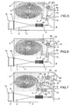
- the optical signal transmission system comprises a laser diode 1 provided with an input facet 1a and an output facet 1b mounted in contact on an input facet of a passive optical chip 2.
- the passive optical chip 2 comprises, on the upper surface, a first waveguide 3 comprising a spreader or adiabatic transition 4 connected at the input to the output facet 1b of the narrow-beam laser diode 1, passing through a reflecting structure 5 at the wavelength of the broadband laser diode 1.
- This portion of the first waveguide 3 forms a modal transformer which terminates with a monomode waveguide 6.
- the first waveguide 3 comprises a portion 7 covered with a thin-film portion 8, active or non-linear powered by the laser diode 1. Then, after passing through the thin-layer portion 8, the first waveguide 8 wave 3 continues and ends with an output end 9 opening on an edge of the passive optical chip 2.
- the passive optical chip 2 comprises, on the upper surface, a second waveguide 10 comprising an input end 11 opening on an edge of the passive optical chip 2 and an input end 12.
- the passive optical chip 2 is provided, on the upper surface, with a first coupler 13 formed by two first portions 14 and 15 of the first waveguide 3, which are not covered by the thin-film portion 8 and are located on both sides. other of the thin-film portion 8 along the optical path, and a second coupler 16 formed by two second portions 17 and 18, respectively of the first and second waveguides 3 and 10, not covered by the layered portion thin 8.
- the figure 1 illustrates the use of the first coupler 13 as pump / signal separator.
- the signal to be amplified enters the end 9 of the first waveguide 3 and, after amplification, leaves the end 11 of the second waveguide 10.
- the architecture represented on the figure 1 is made on the basis of a passive substrate 2 and an active substrate 8, both comprising glass, preferably.
- the architecture shown has three parts.
- the first part comprises the broadband laser diode 1, also called pump diode in the remainder of this document, and is coupled to the input of the modal transformer formed of the adiabatic transition 4 of the first waveguide 3 passing through the structure reflector 5 terminating in a monomode waveguide portion 6 at the pump and signal wavelengths on which the reflective structure 5 is integrated, for example a Bragg grating 5.
- the Bragg wavelength is chosen to be located in the gain band of the pump diode 1 and in the absorption band of the active substrate 8.
- the Bragg grating 5 creates a planar external activity at the pump diode 1 and imposes a monomode and selective feedback in wavelength within the pump diode 1.
- This first part also includes the first coupler 13, two branches of which are connected to the second part.
- the second part comprises a portion 7 of the first waveguide 3, in this case a loop 7, connecting the two output branches of the first coupler 13.
- the amplifying medium 8, or thin-film portion 8, active or non-linear fed by the laser diode 1, is formed on a part of the loop 7.
- the amplifying medium 8 is preferably a thin layer of an active glass carried by molecular adhesion on the passive substrate 2, allowing hybrid guidance within the portion in thin layer 8 where the portion 7 of the first waveguide 3 is present.
- the first coupler 13 is sized to provide, on a single way, a coupling of 3 dB at the wavelength of the pump diode 1 locked by the Bragg grating 5.
- the pump wavelength is symmetrically injected into the amplifier guide formed by the portion 7 of the first waveguide 3 in contact with the amplifying medium 8.
- the residual pump leaving on either side of the amplifier guide 7 and arriving on each of branches of the first coupler 13 couples entirely in the branch by which it arrived.
- the two pump waves separated by the first coupler have traveled the same optical path, also the phase difference between them is due to the phase shift induced by the first coupler 13.
- the two residual waves are in quadrature of phase arriving on the first coupler 13 and all power is transmitted to the branch through which the pump is brought.
- the Bragg grating 5 makes it possible to recycle, at its reflectivity, the pump in the amplifying medium 8.
- the first coupler 13 is also sized to provide a complete transfer of the signal, as illustrated in FIG. figure 1 , or, alternatively, as illustrated on the figure 2 , to offer no coupling from one branch to another for the wavelength of the signal to be amplified.
- the first coupler 13 makes it possible, in the case of figure 1 , to directly mix the pump and the signal, which makes it possible to avoid the presence of a component necessary for the amplification modules.
- the first coupler 13 makes it possible to separate the pump directly from the signal, which also makes it possible to avoid the presence of a component necessary for the amplification modules.
- the end 11 of the second waveguide 10 therefore comprises only the amplified signal and constitutes the output of the system.
- the third part concerns, in the case of figure 1 , the end 11 of the second waveguide, through which the amplified signal, and its separator, or second coupler 16, out of the pump.
- the design of the couplers is such that it is simpler to consider them as black boxes connecting two waveguides on one side to two waveguides on the other side (the terms Inputs / outputs have no real meaning, but serve to differentiate the sides Couplers are not oriented).
- Any wave arriving on a waveguide on one side of a coupler is divided into two waves on the two waveguides, on the other side, with a separation coefficient and a phase (between the output that is in front of the injection waveguide and the one that is opposite) which depends on the characteristics of the coupler, the polarization of the wave and its wavelength.
- These couplers can therefore be used as mixers, separators, or duplexer / wavelength separators as required.
- the wave is not confined in its insertion guide.
- the third part concerns the end 9 by which between the amplified signal, and its mixer, or second coupler 16, with the pump.
- the Figures 3, 4 , and 5 illustrate embodiments for increasing the length of the amplifying medium.
- the embodiment shown on the figure 3 allows to have the two signals to be injected (pump and amplified signal) as well as the output signal (amplified signal) located on the same border of the passive optical chip 2.
- the facets needing to be polished during the manufacture of the system are therefore minimized.
- the embodiment shown on the figure 4 wherein the output of the amplification module system is located on another edge of the passive optical chip 2 than that comprising the pump diode laser diode 1, facilitates the connection of a fiber for extracting the amplified signal.
- the guide in the portion covered by the gain medium, the guide must be at the surface so that the wave can interact with the gain medium 8 while in the rest of the plate 3 the guides must be buried (to limit the diffusion losses on the surface of the plate).
- the transition between the surface guide and the buried guide requires a special method of realization and it is easier to have both transition on the same axis.
- FIGS. 6 and 7 illustrate two embodiments particularly useful for remote sensing laser or LiDAR for acronym for the expression in English language “light detection and ranging”.
- a partial transfer of the input 9 of the signal to the amplifying medium 8 by the second coupler 16 is used.
- a local oscillator channel 20 is then created using the second coupler 16 already present.
- a third waveguide 21 with extremities 22 and 23 is added, a third coupler 24 formed by two third portions 25 and 26 respectively of the second waveguide 10 and the third waveguide 21, and a balanced detector 26 to perform a balanced self-heterodyne detection.
- the ends 12 and 23 of the second and third waveguides 10 and 21 arrive on two photodiodes of the balanced detector 26.
- the approaches and the spacings of the branches of the three couplers 13, 16 and 24 are identical, facilitating their dimensioning.
- the wound part 7 uses a technology allowing a radius of curvature for the waveguides up to 1 mm.
- the radius of curvature may vary depending on the confinement of the guided modes given by the technology employed. The larger the confinement, the smaller the radius of curvature.
- the passive glass may be a silicate glass
- the active glass may be a phosphate glass doped with rare earths.
- the length of the Bragg grating is typically about one centimeter, which brings the minimum extension of the chip 2 in the direction of the spreader 4 to 3 cm.
- a radius of curvature of 4 mm avoids any radiation loss in the curvatures.
- the 2 cm of the amplifying medium and this separation of 500 microns make it possible to obtain a length of amplifier guides 7 of 74 cm.
- the other axis of the ellipse is then 2.8 cm.
- This large length of 74 cm is useful in the case where the active medium has little absorption at the pump wavelength, as is the case for Erbium doped glasses.
- the phosphate glass is then codoped Erbium / Ytterbium in order to increase the absorption cross section at the pump wavelength.
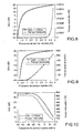
- the calculation of the gain available when the system is carried out by ion exchange on an Erbium / Ytterbium doped phosphate glass can be carried out as follows.
- the simulations are conducted for an injection of the pump on one side of the system.
- the Figures 8 and 9 present the simulation results of the gain obtained as a function of the pump power injected into the active medium 8 for an input signal power of 10 mW.
- the figure 7 relates to the length of the amplifier guide 7 of 50 cm, and the figure 8 relates to the length of amplifier guide 7 of 25 cm.
- an amplifier guide length 7 of 50 cm is too large. Indeed a medium as long implies a pump power of more than 4.5 W to begin to saturate the amplifier over the entire length of the amplifier guide 7.
- a length of 25 cm is better suited.
- a pump power of 4W gives a signal power output of 1 W for an input power of 10mW.
- the figure 10 describes the evolution of the gain as a function of the input signal power injected at the end 9 of the waveguide for a length of the amplifier guide 7 of 25 cm and a pump of 2 W. This calculation shows in particular that an input power of 1 mW reaches 270 mW at the output of the amplifier system and an input power of 1 ⁇ W gives 2.5 mW output.
- This system can be used in areas for which high gain amplification is required and space constraints do not allow the use of conventional solutions. It can also be applied when it is desired to avoid the presence of optical fibers, which are not robust to mechanical vibrations and which can sometimes complicate maintenance.
- embedded systems where congestion is an extremely important parameter, may include the invention, and particularly remote-sensing laser or LiDAR.
- the methods used to implement the invention may use technologies etched or diffused according to the constraints. Yes it is desired to be naturally compatible with the optical fibers, a low index jump technology is preferred. If natural compatibility with the pump laser diode is desired, a high index jump technology is preferred.
- the technology of ion exchange on glass will be used, to satisfy both constraints.
Claims (9)
- System zum Senden eines optischen Signals, das Folgendes umfasst: einen passiven optischen Chip (2), auf seiner Oberseite versehen mit einem ersten Wellenleiter (3) und eine an der Peripherie des passiven optischen Chips (2) angeordnete Breitbandlaserdiode (1), wobei der passive optische Chip (2) auf seiner Oberseite mit einer auf der Wellenlänge der Breitbandlaserdiode (1) reflektierenden Struktur (5) und mit einem aktiven oder nichtlinearen Dünnschichtabschnitt (8) versehen ist, der von der Laserdiode (1) gespeist wird und einen Teil (7) des ersten Wellenleiters (3) bedeckt, wobei der erste Wellenleiter (3) mit der Laserdiode (1) an deren Eingangsende verbunden ist, die reflektierende Struktur (5) durchquert und einen Übergang (4) zwischen einem breiten Eingang des ersten Wellenleiters am Ausgang der Laserdiode (1) und einem schmalen Abschnitt des ersten Wellenleiters (3) umfasst, der die reflektierende Struktur (5) durchquert, wobei der passive optische Chip (2) auf seiner Oberseite versehen ist mit einem zweiten Wellenleiter (10), einem ersten Koppler (13), der von zwei ersten Abschnitten (14, 15) des ersten Wellenleiters (3) gebildet wird, die nicht von dem Dünnschichtabschnitt (8) bedeckt werden und sich auf beiden Seiten des Dünnschichtabschnitts (8) entlang dem optischen Pfad befinden, und einem zweiten Koppler (16), der von zwei nicht von dem Dünnschichtabschnitt (8) bedeckten zweiten Abschnitten (17, 18) jeweils des ersten und zweiten Wellenleiters (3, 10) gebildet wird.
- System nach Anspruch 1, wobei die Ein- und Ausgangsenden des ersten und zweiten Wellenleiters (3, 10), die an einem Rand des passiven optischen Chips (2) münden, am selben Rand des passiven optischen Chips (2) angeordnet sind.
- System nach Anspruch 1 oder 2, wobei die Ein- und Ausgangsenden des ersten und zweiten Wellenleiters (3, 10), die an einem Rand des optischen Chips (2) münden, in einem Abstand von der Laserdiode (1) angeordnet sind.
- System nach einem der vorherigen Ansprüche, wobei der passive optische Chip (2) auf einer Oberseite versehen ist mit einem dritten Wellenleiter (21), einem dritten Koppler (24), der von zwei dritten Abschnitten (25, 26) jeweils des zweiten und dritten Wellenleiters (10, 24) gebildet wird, die nicht von dem dünnschichtigen Abschnitt (8) bedeckt werden, und einem ausgeglichenen Detektionsmodul (26), das mit den Ausgangsenden des zweiten und dritten Wellenleiters (10, 24) an der Peripherie des passiven optischen Chips (2) verbunden ist.
- System nach einem der vorherigen Ansprüche, wobei der von dem dünnschichtigen Abschnitt (8) bedeckte Teil (7) des ersten Wellenleiters (3) gewickelt ist.
- System nach Anspruch 5, bei dem der Krümmungsradius des gewickelten Teils (7) des ersten Wellenleiters (3) größer als 1 mm ist.
- System nach einem der vorherigen Ansprüche, wobei der Übergang (4) adiabatisch ist.
- System nach einem der vorherigen Ansprüche, wobei die Laserdiode (1) eine Ausgangsfacette (1b) umfasst, die antireflektiv behandelt wurde.
- System nach einem der vorherigen Ansprüche, wobei die reflektierende Struktur (5) ein Bragg-Gitter, ein photonisches Kristall, eine Wellenleiterunterbrechung, eine geneigte Facette oder jedwede andere Struktur aufweist, die eine gegen-propagative optische Reflexion zulässt.
Applications Claiming Priority (1)
| Application Number | Priority Date | Filing Date | Title |
|---|---|---|---|
| FR1201997A FR2993415B1 (fr) | 2012-07-13 | 2012-07-13 | Systeme d'emission de signal d'optique |
Publications (2)
| Publication Number | Publication Date |
|---|---|
| EP2685574A1 EP2685574A1 (de) | 2014-01-15 |
| EP2685574B1 true EP2685574B1 (de) | 2015-03-04 |
Family
ID=47553118
Family Applications (1)
| Application Number | Title | Priority Date | Filing Date |
|---|---|---|---|
| EP13176152.0A Active EP2685574B1 (de) | 2012-07-13 | 2013-07-11 | System zum Ausstrahlen eines optischen Signals |
Country Status (4)
| Country | Link |
|---|---|
| US (1) | US9268094B2 (de) |
| EP (1) | EP2685574B1 (de) |
| CA (1) | CA2820829A1 (de) |
| FR (1) | FR2993415B1 (de) |
Families Citing this family (2)
| Publication number | Priority date | Publication date | Assignee | Title |
|---|---|---|---|---|
| WO2016093187A1 (ja) * | 2014-12-10 | 2016-06-16 | 日本碍子株式会社 | 外部共振器型発光装置 |
| US9923634B2 (en) * | 2015-09-23 | 2018-03-20 | Fujitsu Limited | Harmonic generation and phase sensitive amplification using a bragg reflection waveguide |
Family Cites Families (12)
| Publication number | Priority date | Publication date | Assignee | Title |
|---|---|---|---|---|
| US5446749A (en) * | 1994-02-04 | 1995-08-29 | Spectra-Physics Lasers Inc. | Diode pumped, multi axial mode, intracavity doubled laser |
| DE19603704B4 (de) * | 1995-02-15 | 2009-04-09 | Carl Zeiss | Optisch gepumpter Laser mit polarisationsabhängiger Absorption |
| US6052397A (en) * | 1997-12-05 | 2000-04-18 | Sdl, Inc. | Laser diode device having a substantially circular light output beam and a method of forming a tapered section in a semiconductor device to provide for a reproducible mode profile of the output beam |
| WO2002065600A2 (en) * | 2001-02-14 | 2002-08-22 | Gemfire Corporation | Multi-channel laser pump source and packaging method therefor |
| US6944192B2 (en) * | 2001-03-14 | 2005-09-13 | Corning Incorporated | Planar laser |
| US6920159B2 (en) * | 2002-11-29 | 2005-07-19 | Optitune Plc | Tunable optical source |
| WO2004088801A2 (en) * | 2003-03-25 | 2004-10-14 | Lnl Technologies, Inc | External gain element with mode converter and high index contrast waveguide |
| WO2006016410A1 (ja) * | 2004-08-12 | 2006-02-16 | Mitsubishi Denki Kabushiki Kaisha | 基本波光源及び波長変換器 |
| US7532784B2 (en) * | 2006-07-31 | 2009-05-12 | Onechip Photonics Inc. | Integrated vertical wavelength (de)multiplexer |
| JP2010091863A (ja) * | 2008-10-09 | 2010-04-22 | Oki Electric Ind Co Ltd | 送受信モジュール |
| FR2973594B1 (fr) * | 2011-03-31 | 2013-03-29 | Thales Sa | Systeme d'emission de signal optique |
| GB2493585B (en) * | 2011-08-11 | 2013-08-14 | Ibm | Scanning probe microscopy cantilever comprising an electromagnetic sensor |
-
2012
- 2012-07-13 FR FR1201997A patent/FR2993415B1/fr not_active Expired - Fee Related
-
2013
- 2013-07-10 US US13/938,982 patent/US9268094B2/en active Active
- 2013-07-11 CA CA2820829A patent/CA2820829A1/en not_active Abandoned
- 2013-07-11 EP EP13176152.0A patent/EP2685574B1/de active Active
Also Published As
| Publication number | Publication date |
|---|---|
| FR2993415A1 (fr) | 2014-01-17 |
| US9268094B2 (en) | 2016-02-23 |
| US20140119695A1 (en) | 2014-05-01 |
| EP2685574A1 (de) | 2014-01-15 |
| FR2993415B1 (fr) | 2014-08-22 |
| CA2820829A1 (en) | 2014-01-13 |
Similar Documents
| Publication | Publication Date | Title |
|---|---|---|
| US7266258B2 (en) | Two-photon absorption generated carrier lifetime reduction in semiconductor waveguide for semiconductor based raman laser and amplifier | |
| EP0561672B1 (de) | Integrierter optischer Verstärker und Laser mit einem solchen Verstärker | |
| EP0500882B1 (de) | Laser mit gekoppelten optischen wellenleitern | |
| EP3338330B1 (de) | Terahertzlaser, terahertzquelle und verwendung solch eines terahertzlasers | |
| FR2706633A1 (fr) | Dispositif optique comportant une fibre optique amorce et procédé pour sa fabrication. | |
| EP2685574B1 (de) | System zum Ausstrahlen eines optischen Signals | |
| EP2260549B1 (de) | Hochleistungslaserfasersystem | |
| EP2818921B1 (de) | Vorrichtung zur nicht-linearen Signalumwandlung durch Vermischen von vier Wellen | |
| EP2692032B1 (de) | System zur übertragung von optischen signalen | |
| Jones et al. | Hybrid silicon integration | |
| FR2657731A1 (fr) | Amplificateur optique integre. | |
| FR2739195A1 (fr) | Coupleur optique a bande etroite utilisant l'excitation des modes de galerie d'un element resonateur dielectrique de forme de revolution | |
| US20110249689A1 (en) | Devices, systems, and methods providing micro-ring and/or micro-racetrack resonator | |
| WO2009138309A1 (fr) | Dispositif laser monomode de puissance et systeme d'amplication comportant le dispositif laser | |
| EP1030412B1 (de) | Optischer Verstärker | |
| EP3235149A1 (de) | Optoelektronisches bauelement zur erzeugung und aussendung eines hochfrequenzsignals | |
| EP4298460A1 (de) | Optoelektronischer emitter mit phasengesteuerter gruppenantenne mit aufgeweiteter laserquelle | |
| FR2890496A1 (fr) | Procede de production d'un faisceau laser de puissance et dispositif de mise en oeuvre | |
| FR2739732A1 (fr) | Dispositif d'amplification optique | |
| Pipatsart et al. | A proposal of all-wavelength optical amplifiers | |
| WO2005015698A1 (fr) | Source laser de puissance a grande finesse spectrale | |
| Provino et al. | Broadband and flat parametric gain with a single pump in a multi-section nonlinear fiber arrangement | |
| FR2826458A1 (fr) | Element de couplage actif permettant de coupler un signal lumineux a un composant optique a guide d'onde et structure optique utilisant un tel element | |
| WO2003040765A2 (fr) | Dispositif de pompe optique a plusieurs voies de sortie et utilisation du dispositif de pompe dans un dispositif d'amplification | |
| FR2670023A1 (fr) | Dispositif pour combiner ou separer des ondes electromagnetiques de polarisations perpendiculaires entre elles, dispositif amplificateur et dispositif de detection coherente. |
Legal Events
| Date | Code | Title | Description |
|---|---|---|---|
| PUAI | Public reference made under article 153(3) epc to a published international application that has entered the european phase |
Free format text: ORIGINAL CODE: 0009012 |
|
| AK | Designated contracting states |
Kind code of ref document: A1 Designated state(s): AL AT BE BG CH CY CZ DE DK EE ES FI FR GB GR HR HU IE IS IT LI LT LU LV MC MK MT NL NO PL PT RO RS SE SI SK SM TR |
|
| AX | Request for extension of the european patent |
Extension state: BA ME |
|
| RAP3 | Party data changed (applicant data changed or rights of an application transferred) |
Owner name: CENTRE NATIONAL DE LA RECHERCHE SCIENTIFIQUE Owner name: THALES |
|
| 17P | Request for examination filed |
Effective date: 20140414 |
|
| RBV | Designated contracting states (corrected) |
Designated state(s): AL AT BE BG CH CY CZ DE DK EE ES FI FR GB GR HR HU IE IS IT LI LT LU LV MC MK MT NL NO PL PT RO RS SE SI SK SM TR |
|
| GRAP | Despatch of communication of intention to grant a patent |
Free format text: ORIGINAL CODE: EPIDOSNIGR1 |
|
| INTG | Intention to grant announced |
Effective date: 20140930 |
|
| GRAS | Grant fee paid |
Free format text: ORIGINAL CODE: EPIDOSNIGR3 |
|
| GRAA | (expected) grant |
Free format text: ORIGINAL CODE: 0009210 |
|
| AK | Designated contracting states |
Kind code of ref document: B1 Designated state(s): AL AT BE BG CH CY CZ DE DK EE ES FI FR GB GR HR HU IE IS IT LI LT LU LV MC MK MT NL NO PL PT RO RS SE SI SK SM TR |
|
| REG | Reference to a national code |
Ref country code: GB Ref legal event code: FG4D Free format text: NOT ENGLISH |
|
| REG | Reference to a national code |
Ref country code: CH Ref legal event code: EP |
|
| REG | Reference to a national code |
Ref country code: IE Ref legal event code: FG4D Free format text: LANGUAGE OF EP DOCUMENT: FRENCH |
|
| REG | Reference to a national code |
Ref country code: AT Ref legal event code: REF Ref document number: 714586 Country of ref document: AT Kind code of ref document: T Effective date: 20150415 |
|
| REG | Reference to a national code |
Ref country code: DE Ref legal event code: R096 Ref document number: 602013001078 Country of ref document: DE Effective date: 20150416 |
|
| RAP2 | Party data changed (patent owner data changed or rights of a patent transferred) |
Owner name: THALES |
|
| REG | Reference to a national code |
Ref country code: FR Ref legal event code: PLFP Year of fee payment: 3 |
|
| REG | Reference to a national code |
Ref country code: AT Ref legal event code: MK05 Ref document number: 714586 Country of ref document: AT Kind code of ref document: T Effective date: 20150304 Ref country code: NL Ref legal event code: VDEP Effective date: 20150304 |
|
| PG25 | Lapsed in a contracting state [announced via postgrant information from national office to epo] |
Ref country code: FI Free format text: LAPSE BECAUSE OF FAILURE TO SUBMIT A TRANSLATION OF THE DESCRIPTION OR TO PAY THE FEE WITHIN THE PRESCRIBED TIME-LIMIT Effective date: 20150304 Ref country code: NO Free format text: LAPSE BECAUSE OF FAILURE TO SUBMIT A TRANSLATION OF THE DESCRIPTION OR TO PAY THE FEE WITHIN THE PRESCRIBED TIME-LIMIT Effective date: 20150604 Ref country code: ES Free format text: LAPSE BECAUSE OF FAILURE TO SUBMIT A TRANSLATION OF THE DESCRIPTION OR TO PAY THE FEE WITHIN THE PRESCRIBED TIME-LIMIT Effective date: 20150304 Ref country code: HR Free format text: LAPSE BECAUSE OF FAILURE TO SUBMIT A TRANSLATION OF THE DESCRIPTION OR TO PAY THE FEE WITHIN THE PRESCRIBED TIME-LIMIT Effective date: 20150304 Ref country code: LT Free format text: LAPSE BECAUSE OF FAILURE TO SUBMIT A TRANSLATION OF THE DESCRIPTION OR TO PAY THE FEE WITHIN THE PRESCRIBED TIME-LIMIT Effective date: 20150304 Ref country code: SE Free format text: LAPSE BECAUSE OF FAILURE TO SUBMIT A TRANSLATION OF THE DESCRIPTION OR TO PAY THE FEE WITHIN THE PRESCRIBED TIME-LIMIT Effective date: 20150304 |
|
| REG | Reference to a national code |
Ref country code: LT Ref legal event code: MG4D |
|
| PG25 | Lapsed in a contracting state [announced via postgrant information from national office to epo] |
Ref country code: RS Free format text: LAPSE BECAUSE OF FAILURE TO SUBMIT A TRANSLATION OF THE DESCRIPTION OR TO PAY THE FEE WITHIN THE PRESCRIBED TIME-LIMIT Effective date: 20150304 Ref country code: GR Free format text: LAPSE BECAUSE OF FAILURE TO SUBMIT A TRANSLATION OF THE DESCRIPTION OR TO PAY THE FEE WITHIN THE PRESCRIBED TIME-LIMIT Effective date: 20150605 Ref country code: AT Free format text: LAPSE BECAUSE OF FAILURE TO SUBMIT A TRANSLATION OF THE DESCRIPTION OR TO PAY THE FEE WITHIN THE PRESCRIBED TIME-LIMIT Effective date: 20150304 Ref country code: LV Free format text: LAPSE BECAUSE OF FAILURE TO SUBMIT A TRANSLATION OF THE DESCRIPTION OR TO PAY THE FEE WITHIN THE PRESCRIBED TIME-LIMIT Effective date: 20150304 |
|
| PG25 | Lapsed in a contracting state [announced via postgrant information from national office to epo] |
Ref country code: NL Free format text: LAPSE BECAUSE OF FAILURE TO SUBMIT A TRANSLATION OF THE DESCRIPTION OR TO PAY THE FEE WITHIN THE PRESCRIBED TIME-LIMIT Effective date: 20150304 |
|
| PG25 | Lapsed in a contracting state [announced via postgrant information from national office to epo] |
Ref country code: RO Free format text: LAPSE BECAUSE OF FAILURE TO SUBMIT A TRANSLATION OF THE DESCRIPTION OR TO PAY THE FEE WITHIN THE PRESCRIBED TIME-LIMIT Effective date: 20150304 Ref country code: CZ Free format text: LAPSE BECAUSE OF FAILURE TO SUBMIT A TRANSLATION OF THE DESCRIPTION OR TO PAY THE FEE WITHIN THE PRESCRIBED TIME-LIMIT Effective date: 20150304 Ref country code: PT Free format text: LAPSE BECAUSE OF FAILURE TO SUBMIT A TRANSLATION OF THE DESCRIPTION OR TO PAY THE FEE WITHIN THE PRESCRIBED TIME-LIMIT Effective date: 20150706 Ref country code: SK Free format text: LAPSE BECAUSE OF FAILURE TO SUBMIT A TRANSLATION OF THE DESCRIPTION OR TO PAY THE FEE WITHIN THE PRESCRIBED TIME-LIMIT Effective date: 20150304 Ref country code: EE Free format text: LAPSE BECAUSE OF FAILURE TO SUBMIT A TRANSLATION OF THE DESCRIPTION OR TO PAY THE FEE WITHIN THE PRESCRIBED TIME-LIMIT Effective date: 20150304 |
|
| PG25 | Lapsed in a contracting state [announced via postgrant information from national office to epo] |
Ref country code: IS Free format text: LAPSE BECAUSE OF FAILURE TO SUBMIT A TRANSLATION OF THE DESCRIPTION OR TO PAY THE FEE WITHIN THE PRESCRIBED TIME-LIMIT Effective date: 20150704 Ref country code: PL Free format text: LAPSE BECAUSE OF FAILURE TO SUBMIT A TRANSLATION OF THE DESCRIPTION OR TO PAY THE FEE WITHIN THE PRESCRIBED TIME-LIMIT Effective date: 20150304 |
|
| REG | Reference to a national code |
Ref country code: DE Ref legal event code: R097 Ref document number: 602013001078 Country of ref document: DE |
|
| PG25 | Lapsed in a contracting state [announced via postgrant information from national office to epo] |
Ref country code: IT Free format text: LAPSE BECAUSE OF FAILURE TO SUBMIT A TRANSLATION OF THE DESCRIPTION OR TO PAY THE FEE WITHIN THE PRESCRIBED TIME-LIMIT Effective date: 20150304 |
|
| PLBE | No opposition filed within time limit |
Free format text: ORIGINAL CODE: 0009261 |
|
| STAA | Information on the status of an ep patent application or granted ep patent |
Free format text: STATUS: NO OPPOSITION FILED WITHIN TIME LIMIT |
|
| PG25 | Lapsed in a contracting state [announced via postgrant information from national office to epo] |
Ref country code: DK Free format text: LAPSE BECAUSE OF FAILURE TO SUBMIT A TRANSLATION OF THE DESCRIPTION OR TO PAY THE FEE WITHIN THE PRESCRIBED TIME-LIMIT Effective date: 20150304 |
|
| 26N | No opposition filed |
Effective date: 20151207 |
|
| PG25 | Lapsed in a contracting state [announced via postgrant information from national office to epo] |
Ref country code: MC Free format text: LAPSE BECAUSE OF FAILURE TO SUBMIT A TRANSLATION OF THE DESCRIPTION OR TO PAY THE FEE WITHIN THE PRESCRIBED TIME-LIMIT Effective date: 20150304 Ref country code: SI Free format text: LAPSE BECAUSE OF FAILURE TO SUBMIT A TRANSLATION OF THE DESCRIPTION OR TO PAY THE FEE WITHIN THE PRESCRIBED TIME-LIMIT Effective date: 20150304 |
|
| PG25 | Lapsed in a contracting state [announced via postgrant information from national office to epo] |
Ref country code: LU Free format text: LAPSE BECAUSE OF FAILURE TO SUBMIT A TRANSLATION OF THE DESCRIPTION OR TO PAY THE FEE WITHIN THE PRESCRIBED TIME-LIMIT Effective date: 20150711 |
|
| REG | Reference to a national code |
Ref country code: IE Ref legal event code: MM4A |
|
| REG | Reference to a national code |
Ref country code: FR Ref legal event code: PLFP Year of fee payment: 4 |
|
| PG25 | Lapsed in a contracting state [announced via postgrant information from national office to epo] |
Ref country code: IE Free format text: LAPSE BECAUSE OF NON-PAYMENT OF DUE FEES Effective date: 20150711 |
|
| REG | Reference to a national code |
Ref country code: CH Ref legal event code: PL |
|
| PG25 | Lapsed in a contracting state [announced via postgrant information from national office to epo] |
Ref country code: MT Free format text: LAPSE BECAUSE OF FAILURE TO SUBMIT A TRANSLATION OF THE DESCRIPTION OR TO PAY THE FEE WITHIN THE PRESCRIBED TIME-LIMIT Effective date: 20150304 |
|
| PG25 | Lapsed in a contracting state [announced via postgrant information from national office to epo] |
Ref country code: LI Free format text: LAPSE BECAUSE OF NON-PAYMENT OF DUE FEES Effective date: 20160731 Ref country code: CH Free format text: LAPSE BECAUSE OF NON-PAYMENT OF DUE FEES Effective date: 20160731 |
|
| PG25 | Lapsed in a contracting state [announced via postgrant information from national office to epo] |
Ref country code: BG Free format text: LAPSE BECAUSE OF FAILURE TO SUBMIT A TRANSLATION OF THE DESCRIPTION OR TO PAY THE FEE WITHIN THE PRESCRIBED TIME-LIMIT Effective date: 20150304 Ref country code: HU Free format text: LAPSE BECAUSE OF FAILURE TO SUBMIT A TRANSLATION OF THE DESCRIPTION OR TO PAY THE FEE WITHIN THE PRESCRIBED TIME-LIMIT; INVALID AB INITIO Effective date: 20130711 |
|
| REG | Reference to a national code |
Ref country code: FR Ref legal event code: PLFP Year of fee payment: 5 |
|
| PG25 | Lapsed in a contracting state [announced via postgrant information from national office to epo] |
Ref country code: CY Free format text: LAPSE BECAUSE OF FAILURE TO SUBMIT A TRANSLATION OF THE DESCRIPTION OR TO PAY THE FEE WITHIN THE PRESCRIBED TIME-LIMIT Effective date: 20150304 |
|
| PG25 | Lapsed in a contracting state [announced via postgrant information from national office to epo] |
Ref country code: BE Free format text: LAPSE BECAUSE OF NON-PAYMENT OF DUE FEES Effective date: 20150731 |
|
| PG25 | Lapsed in a contracting state [announced via postgrant information from national office to epo] |
Ref country code: SM Free format text: LAPSE BECAUSE OF FAILURE TO SUBMIT A TRANSLATION OF THE DESCRIPTION OR TO PAY THE FEE WITHIN THE PRESCRIBED TIME-LIMIT Effective date: 20150304 |
|
| REG | Reference to a national code |
Ref country code: FR Ref legal event code: PLFP Year of fee payment: 6 |
|
| PG25 | Lapsed in a contracting state [announced via postgrant information from national office to epo] |
Ref country code: MK Free format text: LAPSE BECAUSE OF FAILURE TO SUBMIT A TRANSLATION OF THE DESCRIPTION OR TO PAY THE FEE WITHIN THE PRESCRIBED TIME-LIMIT Effective date: 20150304 Ref country code: TR Free format text: LAPSE BECAUSE OF FAILURE TO SUBMIT A TRANSLATION OF THE DESCRIPTION OR TO PAY THE FEE WITHIN THE PRESCRIBED TIME-LIMIT Effective date: 20150304 |
|
| PG25 | Lapsed in a contracting state [announced via postgrant information from national office to epo] |
Ref country code: AL Free format text: LAPSE BECAUSE OF FAILURE TO SUBMIT A TRANSLATION OF THE DESCRIPTION OR TO PAY THE FEE WITHIN THE PRESCRIBED TIME-LIMIT Effective date: 20150304 |
|
| PGFP | Annual fee paid to national office [announced via postgrant information from national office to epo] |
Ref country code: GB Payment date: 20180628 Year of fee payment: 6 Ref country code: DE Payment date: 20180626 Year of fee payment: 6 |
|
| REG | Reference to a national code |
Ref country code: DE Ref legal event code: R119 Ref document number: 602013001078 Country of ref document: DE |
|
| GBPC | Gb: european patent ceased through non-payment of renewal fee |
Effective date: 20190711 |
|
| PG25 | Lapsed in a contracting state [announced via postgrant information from national office to epo] |
Ref country code: DE Free format text: LAPSE BECAUSE OF NON-PAYMENT OF DUE FEES Effective date: 20200201 Ref country code: GB Free format text: LAPSE BECAUSE OF NON-PAYMENT OF DUE FEES Effective date: 20190711 |
|
| P01 | Opt-out of the competence of the unified patent court (upc) registered |
Effective date: 20230427 |
|
| PGFP | Annual fee paid to national office [announced via postgrant information from national office to epo] |
Ref country code: FR Payment date: 20230622 Year of fee payment: 11 |