EP2681741B1 - System and method for bonded configuration pad continuity check - Google Patents
System and method for bonded configuration pad continuity check Download PDFInfo
- Publication number
- EP2681741B1 EP2681741B1 EP12712431.1A EP12712431A EP2681741B1 EP 2681741 B1 EP2681741 B1 EP 2681741B1 EP 12712431 A EP12712431 A EP 12712431A EP 2681741 B1 EP2681741 B1 EP 2681741B1
- Authority
- EP
- European Patent Office
- Prior art keywords
- pull
- boundary pad
- continuity
- transistor
- output
- Prior art date
- Legal status (The legal status is an assumption and is not a legal conclusion. Google has not performed a legal analysis and makes no representation as to the accuracy of the status listed.)
- Not-in-force
Links
- 238000000034 method Methods 0.000 title claims description 23
- 238000012360 testing method Methods 0.000 claims description 190
- 239000004020 conductor Substances 0.000 claims description 42
- 230000003139 buffering effect Effects 0.000 claims description 2
- 239000000758 substrate Substances 0.000 description 41
- 239000004065 semiconductor Substances 0.000 description 9
- 238000003860 storage Methods 0.000 description 4
- 238000007792 addition Methods 0.000 description 2
- 230000004075 alteration Effects 0.000 description 2
- 230000008901 benefit Effects 0.000 description 2
- 238000013500 data storage Methods 0.000 description 2
- 238000004519 manufacturing process Methods 0.000 description 2
- 239000000463 material Substances 0.000 description 2
- 230000003287 optical effect Effects 0.000 description 2
- 230000001681 protective effect Effects 0.000 description 2
- XUIMIQQOPSSXEZ-UHFFFAOYSA-N Silicon Chemical compound [Si] XUIMIQQOPSSXEZ-UHFFFAOYSA-N 0.000 description 1
- 230000008859 change Effects 0.000 description 1
- 238000004590 computer program Methods 0.000 description 1
- 238000010276 construction Methods 0.000 description 1
- 230000008878 coupling Effects 0.000 description 1
- 238000010168 coupling process Methods 0.000 description 1
- 238000005859 coupling reaction Methods 0.000 description 1
- 239000003989 dielectric material Substances 0.000 description 1
- 238000009792 diffusion process Methods 0.000 description 1
- 230000005055 memory storage Effects 0.000 description 1
- 238000001465 metallisation Methods 0.000 description 1
- 230000008569 process Effects 0.000 description 1
- 238000011112 process operation Methods 0.000 description 1
- 239000000523 sample Substances 0.000 description 1
- 230000008054 signal transmission Effects 0.000 description 1
- 229910052710 silicon Inorganic materials 0.000 description 1
- 239000010703 silicon Substances 0.000 description 1
- 230000009466 transformation Effects 0.000 description 1
Images



Classifications
-
- G—PHYSICS
- G11—INFORMATION STORAGE
- G11C—STATIC STORES
- G11C29/00—Checking stores for correct operation ; Subsequent repair; Testing stores during standby or offline operation
- G11C29/02—Detection or location of defective auxiliary circuits, e.g. defective refresh counters
-
- G—PHYSICS
- G11—INFORMATION STORAGE
- G11C—STATIC STORES
- G11C29/00—Checking stores for correct operation ; Subsequent repair; Testing stores during standby or offline operation
- G11C29/02—Detection or location of defective auxiliary circuits, e.g. defective refresh counters
- G11C29/022—Detection or location of defective auxiliary circuits, e.g. defective refresh counters in I/O circuitry
-
- G—PHYSICS
- G01—MEASURING; TESTING
- G01R—MEASURING ELECTRIC VARIABLES; MEASURING MAGNETIC VARIABLES
- G01R31/00—Arrangements for testing electric properties; Arrangements for locating electric faults; Arrangements for electrical testing characterised by what is being tested not provided for elsewhere
- G01R31/28—Testing of electronic circuits, e.g. by signal tracer
-
- G—PHYSICS
- G01—MEASURING; TESTING
- G01R—MEASURING ELECTRIC VARIABLES; MEASURING MAGNETIC VARIABLES
- G01R31/00—Arrangements for testing electric properties; Arrangements for locating electric faults; Arrangements for electrical testing characterised by what is being tested not provided for elsewhere
- G01R31/28—Testing of electronic circuits, e.g. by signal tracer
- G01R31/317—Testing of digital circuits
-
- G—PHYSICS
- G01—MEASURING; TESTING
- G01R—MEASURING ELECTRIC VARIABLES; MEASURING MAGNETIC VARIABLES
- G01R31/00—Arrangements for testing electric properties; Arrangements for locating electric faults; Arrangements for electrical testing characterised by what is being tested not provided for elsewhere
- G01R31/50—Testing of electric apparatus, lines, cables or components for short-circuits, continuity, leakage current or incorrect line connections
- G01R31/54—Testing for continuity
Definitions
- Non-volatile semiconductor memory devices such as flash memory cards and the like, have become an essential component for digital information storage in modem electronic devices.
- modem portable electronic devices benefit greatly from the high-capacity, versatility, ruggedness, and power utilization efficiency afforded by semiconductor memory devices.
- Such modem portable electronic devices may include, by way of example, digital cameras, digital music players, smart phones, video game consoles, portable computing devices, among others.
- Flash memory storage cards may be fabricated as a system-in-a-package (SIP) or as a multichip module (MCM), in which multiple semiconductor die are mounted and interconnected on a substrate.
- the substrate may include a rigid, dielectric base with a conductive layer etched on one or both sides.
- the die are electrically connected to the conductive layer(s) of the substrate.
- the conductive layer(s) of the substrate provide for electrical connection of the die to a host electronic device.
- the die/substrate assembly may be encased in a protective material, which also assists in holding the die and substrate together.
- Connection of the die to the substrate can include connection of electrically conductive pads on the die to wire bonds on the substrate.
- the connections between the pads of the die and the wire bonds of the substrate are often inaccessible for continuity testing once the die is placed on the substrate, and especially after the die and substrate are encased in the protective material.
- US 2009/0066362 A1 discloses a semiconductor integrated circuit having a test circuit for inspecting states of connections between a plurality of pads and respective external terminals by bonding wires.
- US 2009/0027059 A1 discloses a technique of detecting an open integrated circuit (IC) pin which includes selectably coupling a first open detect circuit, which includes a first inverter having a first threshold, to the IC pin.
- US 2008/0290341 A1 discloses a stacked semiconductor device which includes: an internal circuit; a through electrode provided to penetrate through a semiconductor substrate; a test wiring to which a predetermined potential different from a substrate potential is supplied at a time of a test; a first switch arranged between the through electrode and the internal circuit; a second switch arranged between the through electrode and the test wiring; and a control circuit that exclusively turns on the first and the second switches.
- a continuity test circuit for a boundary pad.
- the continuity test circuit comprises a pull-up transistor electrically connected between the boundary pad and a first power supply, a pull-down transistor electrically connected between the boundary pad and a first reference ground potential, a normal output conductor electrically connected to have a same electrical state as the boundary pad during normal operation, and a continuity test output conductor electrically connected to have a same electrical state as the boundary pad during continuity test operation.
- the continuity test circuit further comprises continuity testing control circuitry defined to control the pull-up transistor, the pull-down transistor, and the normal output conductor during continuity test operation such that an electrical state present on the continuity test output conductor indicates a status of electrical continuity between the boundary pad and either a second power supply or a second reference ground potential to which the boundary pad should be electrically connected.
- the continuity testing control circuitry includes a pull-up control multiplexer defined to control a gate of the pull-up transistor in accordance with an operation control signal.
- the continuity testing control circuitry includes a pull-down control multiplexer defined to control a gate of the pull-down transistor in accordance with the operation control signal.
- the continuity testing control circuitry includes an output control multiplexer defined to persist a normal operation output signal to the normal output conductor in accordance with the operation control signal.
- the output control multiplexer is defined to have a first input connected to receive the electrical state present at the boundary pad and a second input connected to receive an output override signal.
- An output of the output control multiplexer is electrically connected to the normal output conductor, such that when the operation control signal indicates normal operation mode the electrical state present at the boundary pad is transmitted by the output control multiplexer to the normal output conductor, and such that when the operation control signal indicates continuity test operation mode the output override signal is transmitted by the output control multiplexer to the normal output conductor.
- a method for testing electrical continuity between a boundary pad and a wire bond comprises determining whether the wire bond is electrically connected to either an energized power supply or a reference ground potential. If the wire bond is connected to the energized power supply, a pull-up transistor connected to the boundary pad is turned off, and a pull-down transistor connected to the boundary pad is turned on, and a signal present at the boundary pad is observed to determine whether the signal represents a high digital state or a low digital state. The high digital state indicates electrical continuity between the boundary pad and the wire bond, and the low digital state indicates an absence of electrical continuity between the boundary pad and the wire bond.
- the method further comprises electrically isolating the boundary pad from core circuitry to which the boundary pad is normally connected, and transmitting a signal expected from the boundary pad during normal operation to the core circuitry when the boundary pad is electrically isolated from the core circuitry.
- a continuity test circuit for a boundary pad includes a pull-up transistor electrically connected between the boundary pad and a first power supply.
- the continuity test circuit also includes a pull-down transistor electrically connected between the boundary pad and a first reference ground potential.
- the continuity test circuit also includes a normal output conductor electrically connected to have a same electrical state as the boundary pad during normal operation.
- the continuity test circuit also includes a continuity test output conductor electrically connected to have a same electrical state as the boundary pad during continuity test operation.
- the continuity test circuit includes continuity testing control circuitry defined to control the pull-up transistor, the pull-down transistor, and the normal output conductor during continuity test operation, such that an electrical state present on the continuity test output conductor indicates a status of electrical continuity between the boundary pad and either a second power supply or a second reference ground potential to which the boundary pad should be electrically connected.
- a memory system is disclosed to include a substrate and a die.
- the substrate includes a number of wire bonds.
- the die includes a number of boundary pads. The die is secured to the substrate such that the number of boundary pads are electrically and respectively connected to the number of wire bonds.
- the die also includes continuity test circuitry for each boundary pad. The continuity test circuitry for a given boundary pad is defined to enable firmware controlled testing of electrical continuity between the given boundary pad and its wire bond.
- a method for testing electrical continuity between a boundary pad and a wire bond includes an operation for determining whether the wire bond is electrically connected to either an energized power supply or a reference ground potential. If the wire bond is connected to the energized power supply, the method proceeds with a first set of operations.
- the first set of operation include turning off a pull-up transistor connected to the boundary pad, and turning on a pull-down transistor connected to the boundary pad.
- the first set of operations also include observing a signal present at the boundary pad to determine whether the signal represents a high digital state or a low digital state.
- the method proceeds with a second set of operations.
- the second set of operations include turning on the pull-up transistor connected to the boundary pad, and turning off the pull-down transistor connected to the boundary pad.
- the second set of operations also include observing the signal present at the boundary pad to determine whether the signal represents the high digital state or the low digital state. If the wire bond is connected to the reference ground potential, the low digital state indicates electrical continuity between the boundary pad and the wire bond, and the high digital state indicates an absence of electrical continuity between the boundary pad and the wire bond.
- Figures 1A and 1B show conventional boundary pad configurations that may occur on a die.
- the boundary pad 100 is electrically connected to a power supply 103 by way of a wire bond 123.
- the boundary pad 100 is also electrically connected to a buffer 101.
- the output of the buffer 101 is connected to a normal output conductor 107, along which an electrical signal (cout) may be transmitted from the boundary pad 100 to other circuitry on the die, such as core logic circuitry.
- the boundary pad 100 is also connected to the buffer 101, which is in turn connected to the normal output conductor 107.
- the boundary pad 100 is electrically connected to a reference ground potential 105 by way of a wire bond 123.
- Figure 1C shows a memory system 120 that includes a die 121 connected to a substrate 130.
- the die 121 includes a number of boundary pads 100, such as described with regard to Figures 1A and 1B .
- each boundary pad 100 is supposed to be electrically connected to a corresponding wire bond 123 present on the substrate 130.
- Each wire bond 123 is connected to either the power supply 103 or the reference ground potential 105.
- the boundary pads 100 are not physically accessible after the die 121 is connected to the substrate 130. In these embodiments, it is not possible to visually inspect the electrical continuity between the boundary pad 100 and its wire bond 123.
- FIG. 2A shows a continuity test circuit for a boundary pad 100, in accordance with one embodiment of the present invention.
- the continuity test circuit includes a pull-up transistor 201 that is electrically connected between the boundary pad 100 and a first power supply 203.
- the boundary pad 100 is electrically connected through the pull-up transistor 201 to the first power supply 203 when the pull-up transistor 201 is on.
- the boundary pad 100 is electrically isolated from the first power supply 203 by the pull-up transistor 201 when the pull-up transistor 201 is off.
- the continuity test circuit also includes a pull-down transistor 205 that is electrically connected between the boundary pad 100 and a first reference ground potential 207.
- the boundary pad 100 is electrically connected through the pull-down transistor 205 to the first reference ground potential 207 when the pull-down transistor 205 is on.
- the boundary pad 100 is electrically isolated from the first reference ground potential 207 by the pull-down transistor 205 when the pull-down transistor 205 is off. It should be understood that the pull-up transistor 210, the pull-down transistor 205, the first power supply 203, and the first reference ground potential 207 are defined within a die 200.
- the continuity test circuit also includes the normal output conductor 107 electrically connected to have a same electrical state as the boundary pad 100 during normal operation, as discussed in more detail below.
- the continuity test circuit further includes a continuity test output conductor 209 electrically connected to have a same electrical state as the boundary pad 100 during continuity test operation.
- the normal output conductor 107 and the continuity test output conductor 109 are both electrically connected to the boundary pad 100 through a buffer 101. More specifically, the buffer 100 has an input 101A electrically connected to the boundary pad 100, and an output 101B electrically connected to the continuity test output conductor 109. As discussed in more detail below, an electrical signal present at the output 101B of the buffer 101 is transmitted to the normal output conductor 107 under the direction of an output control multiplexer 215, during normal operation.
- the continuity test circuit also includes continuity testing control circuitry defined to control the pull-up transistor 201, the pull-down transistor 205, and the normal output conductor 107 during continuity test operation such that an electrical state present on the continuity test output conductor 209 indicates a status of electrical continuity between the boundary pad 100 and either a second power supply 103 or a second reference ground potential 105 to which the boundary pad 100 should be electrically connected.
- Figure 3A shows the case where the boundary pad 100 is electrically connected to the second reference ground potential 105.
- the boundary pad 100 is physically connected to a wire bond 123 to establish the electrical continuity between the boundary pad 100 and either the second power supply 103 or the second reference ground potential 105, as the case may be. Therefore, for the boundary pad 100 connected to the second power supply 103, electrical continuity between the boundary pad 100 and the second power supply 103 is indicative of whether or not the boundary pad 100 is physically connected to its wire bond 123. And, for the boundary pad 100 connected to the second reference ground potential 105, electrical continuity between the boundary pad 100 and the second reference ground potential 105 is indicative of whether or not the boundary pad 100 is physically connected to its wire bond 123.
- the wire bond 123, second power supply 103, and second reference ground potential 105 are defined within the substrate 130 to which the die 200 is connected.
- the first power supply 203 and the second power supply 103 are equivalent.
- the first power supply 203 and the second power supply 103 are different.
- the first reference ground potential 207 and the second reference ground potential 105 are equivalent.
- the first reference ground potential 207 and the second reference ground potential 105 are different.
- the continuity testing control circuitry includes a pull-up control multiplexer 211 defined to control a gate 201A of the pull-up transistor 201, in accordance with an operation control signal (bypass_en).
- the pull-up control multiplexer 211 is defined to include a select input 211D electrically connected to a continuity testing enable register 217 in which the operation control signal (bypass_en) is set.
- the operation control signal (bypass_en) is set within the continuity testing enable register 217 to indicate either a normal operation mode or a continuity test operation mode.
- the operation control signal (bypass_en) is set within the continuity testing enable register 217 through firmware 219.
- the pull-up control multiplexer 211 is also defined to have a first input 211A connected to receive a pull-up transistor normal control signal (pu_n_f).
- the pull-up control multiplexer 211 is defined to have a second input 211B connected to receive a pull-up transistor test control signal (pu_n_fw).
- the pull-up control multiplexer 211 further includes an output 211C electrically connected to the gate 201 A of the pull-up transistor 201.
- the pull-up transistor normal control signal (pu_n_f) is transmitted by the pull-up control multiplexer 211 to the gate 201A of the pull-up transistor 201.
- the pull-up transistor normal control signal (pu_n_f) is generated through the firmware 219, and may correspond to either a high digital state signal (1) or a low digital state signal (0), depending on the normal operation requirements associated with the boundary pad 100.
- the pull-up transistor test control signal (pu_n_fw) is transmitted by the pull-up control multiplexer 211 to the gate 201A of the pull-up transistor 201.
- the pull-up transistor test control signal (pu_n_fw) is generated through the firmware 219, and may correspond to either a high digital state signal (1) or a low digital state signal (0), depending on whether the boundary pad 100 is supposed to connect to the second power supply 103 or to the second reference ground potential 105.
- the firmware 219 operates to set the pull-up transistor test control signal (pu_n_fw) to the low digital state signal (0), such that the pull-up transistor 201 will be turned off when the operation control signal (bypass_en) causes the pull-up transistor test control signal (pu_n_fw) to be transmitted through the pull-up control multiplexer 211 to the gate 201A of the pull-up transistor 201.
- the firmware 219 operates to set the pull-up transistor test control signal (pu_n_fw) to the high digital state signal (1), such that the pull-up transistor 201 will be turned on when the operation control signal (bypass_en) causes the pull-up transistor test control signal (pu_n_fw) to be transmitted through the pull-up control multiplexer 211 to the gate 201A of the pull-up transistor 201.
- the continuity testing control circuitry also includes a pull-down control multiplexer 213 defined to control a gate 205A of the pull-down transistor 205, in accordance with the operation control signal (bypass_en).
- the pull-down control multiplexer 213 is defined to include a select input 213D electrically connected to the continuity testing enable register 217 in which the operation control signal (bypass_en) is set.
- the pull-down control multiplexer 213 is also defined to have a first input 213A connected to receive a pull-down transistor normal control signal (pd_n_f).
- the pull-down control multiplexer 213 is defined to have a second input 213B connected to receive a pull-down transistor test control signal (pd_n_fw).
- the pull-down control multiplexer 213 further includes an output 213C electrically connected to the gate 205A of the pull-down transistor 205.
- the pull-down transistor normal control signal (pd_n_f) is transmitted by the pull-down control multiplexer 213 to the gate 205A of the pull-down transistor 205.
- the pull-down transistor normal control signal (pd_n_f) is generated through the firmware 219, and may correspond to either a high digital state signal (1) or a low digital state signal (0), depending on the normal operation requirements associated with the boundary pad 100.
- the pull-down transistor test control signal (pd_n_fw) is transmitted by the pull-down control multiplexer 213 to the gate 205A of the pull-down transistor 205.
- the pull-down transistor test control signal (pd_n_fw) is generated through the firmware 219, and may correspond to either a high digital state signal (1) or a low digital state signal (0), depending on whether the boundary pad 100 is supposed to connect to the second power supply 103 or to the second reference ground potential 105.
- the firmware 219 operates to set the pull-down transistor test control signal (pd_n_fw) to the high digital state signal (1), such that the pull-down transistor 205 will be turned on when the operation control signal (bypass_en) causes the pull-down transistor test control signal (pd_n_fw) to be transmitted through the pull-down control multiplexer 213 to the gate 205A of the pull-down transistor 205.
- the firmware 219 operates to set the pull-down transistor test control signal (pd_n_fw) to the low digital state signal (0), such that the pull-down transistor 205 will be turned off when the operation control signal (bypass_en) causes the pull-down transistor test control signal (pd_n_fw) to be transmitted through the pull-down control multiplexer 213 to the gate 205A of the pull-down transistor 205.
- the continuity testing control circuitry also includes the output control multiplexer 215 defined to persist a normal operation output signal (cout) to the normal output conductor 107, in accordance with the operation control signal (bypass_en).
- the output control multiplexer 215 is defined to include a select input 215D electrically connected to the continuity testing enable register 217 in which the operation control signal (bypass_en) is set.
- the output control multiplexer 215 is also defined to have a first input 215A connected to receive the electrical state present at the boundary pad 100. More specifically, the first input 215A of the output control multiplexer 215 is electrically connected to the output 101B of the buffer 101.
- the first input 215A of the output control multiplexer 215 is connected to receive the electrical state present at the boundary pad 100.
- the output control multiplexer 215 is also defined to have a second input 215B connected to receive an output override signal (cout_override_fw).
- the output control multiplexer 215 also includes an output 215C that is electrically connected to the normal output conductor 107.
- the output control multiplexer 215 is defined such that when the operation control signal (bypass_en) indicates normal operation mode, the electrical state present at the first input 215A of the output control multiplexer 215 is transmitted by the output control multiplexer 215 to the normal output conductor 107. Therefore, when the operation control signal (bypass_en) indicates normal operation mode, the electrical state present at the boundary pad 100 is transmitted through the output control multiplexer 215 to the normal output conductor 107.
- the output override signal (cout_override_fw) is transmitted by the output control multiplexer 215 to the normal output conductor 107.
- the output override signal (cout_override_fw) is used to persist an expected normal operation output signal (cout) to the normal output conductor 107 during the continuity test operation mode. In this manner, any electrical state change at the boundary pad 100 during performance of the continuity testing will be hidden from other circuitry connected to receive the normal operation output signal (cout) from the boundary pad 100. Therefore, continuity testing on the boundary pad 100, as disclosed herein, can be performed without any potential disruption of the normal operation output signal (cout) expected by other circuitry, e.g., core circuitry, connected to the boundary pad 100.
- the output override signal (cout_override_fw) is generated through the firmware 219.
- the output override signal (cout_override_fw) is set to indicate a high digital state (1).
- the output override signal (cout_override_fw) is set to indicate a low digital state (0). Therefore, by way of the output override signal (cout_override_fw) and the output control multiplexer 215, a correct electrical signal is provided at the normal output conductor 107 during the continuity test operation mode.
- FIG. 2A shows the continuity test circuit for the boundary pad 100 on the die 200, in which the boundary pad 100 is supposed to be electrically connected to the second power supply 103 on the substrate 130, in accordance with one embodiment of the present invention.
- the continuity test circuit provides for testing of the electrical continuity between the boundary pad 100 on the die 200 and the wire bond 123 on the substrate 130.
- the operation control signal (bypass_en) is set to a high digital state (1) to enter the continuity test operation mode. It should be understood that in another embodiment with reversed inputs on each of the pull-up control multiplexer 211, pull-down control multiplexer 213, and output control multiplexer 215, the operation control signal (bypass_en) could be set to a low digital state (0) to enter the continuity test operation mode.
- the high digital state (1) of the operation control signal (bypass_en) triggers the continuity test operation mode.
- the electrical signal present at the continuity test output conductor 209 i.e., the continuity test output signal (cout_fw)
- the continuity test output signal (cout_fw) corresponds to a high digital state (1)
- electrical continuity does exist between the boundary pad 100 and the wire bond 123 to which the second power supply 103 is connected.
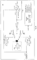
- Figure 2B shows the digital states present within the continuity test circuit of Figure 2A when the continuity test is performed and electrical continuity does exist between the boundary pad 100 and the wire bond 123 to which the second power supply 103 is connected, in accordance with one embodiment of the present invention.
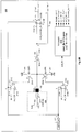
- FIG. 2C shows the digital states present within the continuity test circuit of Figure 2A when the continuity test is performed and electrical continuity does not exist between the boundary pad 100 and the wire bond 123 to which the second power supply 103 is connected, in accordance with one embodiment of the present invention.
- Figure 3A shows the continuity test circuitry of Figure 2A , with the boundary pad 100 on the die 200 electrically connected to the second reference ground potential 105 on the substrate 130, in accordance with one embodiment of the present invention.
- the following settings are implemented through operation of the firmware 219:
- the electrical signal present at the continuity test output conductor 209 i.e., the continuity test output signal (cout_fw)
- the continuity test output signal (cout_fw) corresponds to a low digital state (0)
- electrical continuity does exist between the boundary pad 100 and the wire bond 123 to which the second reference ground potential 105 is connected.
- Figure 3B shows the digital states present within the continuity test circuit of Figure 3A when the continuity test is performed and electrical continuity does exist between the boundary pad 100 and the wire bond 123 to which the second reference ground potential 105 is connected, in accordance with one embodiment of the present invention.
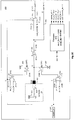
- FIG. 3C shows the digital states present within the continuity test circuit of Figure 3A when the continuity test is performed and electrical continuity does not exist between the boundary pad 100 and the wire bond 123 to which the second reference ground potential 105 is connected, in accordance with one embodiment of the present invention.
- Figure 4 shows a memory system 400 that includes the die 200 connected to the substrate 130, in which the die 200 includes continuity test circuitry 401 for each of its boundary pads 100, in accordance with one embodiment of the present invention.
- the substrate 130 includes the number of wire bonds 123. Some of the wire bonds 123 are electrically connected to the second power supply 103 on the substrate, and some of the wire bonds 123 are electrically connected to the second reference ground potential 105.
- the die 200 includes a number of boundary pads 100. The die 200 is secured to the substrate 130 such that the number of boundary pads 100 are electrically and respectively connected to the number of wire bonds 123.
- the die 200 includes continuity test circuitry 401 for each boundary pad 100.
- the continuity test circuitry 401 for a given boundary pad 100 is defined to enable firmware 219 controlled testing of electrical continuity between the given boundary pad 100 and its wire bond 123. It should be understood that when the die 200 is secured to the substrate 130, the number of boundary pads 100 are not physically accessible from outside the memory system 400.
- the continuity test circuitry 401 for each boundary pad 100 includes the pull-up transistor 201, the pull-up control multiplexer 211, the pull-down transistor 205, the pull-down control multiplexer 213, the output control multiplexer 215, the continuity test output conductor 209, the normal output conductor 107, the continuity testing enable register 217, the firmware 219, and their respective electrical connections as described with regard to each of Figures 2A and 3A . Therefore, the continuity test circuitry 401 is defined to test electrical continuity between a given boundary pad 100 and its wire bond 123 without disrupting an expected signal transmission from the given boundary pad 100 to a core 407 of the die 200.
- the signals used to operate the continuity test circuitry 401 are programmable through a central processing unit of a host device to which the memory system 400 is connected.
- each of the pull-up transistor test control signal (pu_n_fw), the pull-down transistor test control signal (pd_n_fw), the output override signal (cout_override_fw), and the operation control signal (bypass_en) can be programmed in a respective register through the host device to which the memory system 400 is connected.
- the host device can send a command to the firmware 219 to initiate the continuity testing, i.e., to set the operation control signal (bypass_en) in the continuity testing enable register 217 to the high digital state (1).
- the host can direct the firmware 219 to perform the continuity testing on each boundary pad 100, i.e., to poll each boundary pad 100, and check the continuity status of each boundary pad 100.
- Figure 5 shows a flowchart of a method for testing electrical continuity between a boundary pad 100 and a wire bond 123, in accordance with one embodiment of the present invention.
- the method includes an operation 501 for determining whether the wire bond 123 is electrically connected to either an energized power supply 103 or a reference ground potential 105. If the wire bond 123 is connected to the energized power supply 103, the method proceeds with an operation 503 for turning off a pull-up transistor 201 connected to the boundary pad 100. An operation 505 is also performed to turn on a pull-down transistor 205 connected to the boundary pad 100. It should be understood that operations 503 and 505 can be performed in a substantially simultaneous manner.
- an operation 507 is performed to observe a signal present at the boundary pad 100 to determine whether the signal represents a high digital state or a low digital state. Observation of the high digital state in operation 507 indicates electrical continuity between the boundary pad 100 and the wire bond 123. Observation of the low digital state in operation 507 indicates an absence of electrical continuity between the boundary pad 100 and the wire bond 123.
- the method proceeds with an operation 509 for turning on the pull-up transistor 201 connected to the boundary pad 100.
- An operation 511 is also performed to turn off the pull-down transistor 205 connected to the boundary pad 100. It should be understood that operations 509 and 511 can be performed in a substantially simultaneous manner.
- an operation 513 is performed to observe a signal present at the boundary pad 100 to determine whether the signal represents a high digital state or a low digital state. Observation of the low digital state in operation 513 indicates electrical continuity between the boundary pad 100 and the wire bond 123. Observation of the high digital state in operation 513 indicates an absence of electrical continuity between the boundary pad 100 and the wire bond 123.
- the method of Figure 5 also includes an operation for electrically isolating the boundary pad 100 from core circuitry 407 to which the boundary pad 100 is normally connected.
- a signal expected from the boundary pad 100 during normal operation is transmitted to the core circuitry 407 when the boundary pad 100 is electrically isolated from the core circuitry 407.
- the method of Figure 5 can include an operation for buffering the signal present at the boundary pad 100 prior to observing the signal present at the boundary pad 100 in operations 507 and 513 to determine whether the signal represents a high digital state or a low digital state.
- continuity test circuitry dies, substrates, memory systems, memory components, memory chips, memory controller, etc., as discussed herein, can include additional circuitry and components that are not described herein to avoid unnecessarily obscuring the present invention.
- continuity test circuitry disclosed herein is defined to be compatible and interface with the additional circuitry of the various dies, substrates, memory systems, memory components, memory chips, memory controller, etc.
- continuity test circuitry of the embodiments disclosed herein can be efficiently implemented in existing memory systems.
- the continuity test circuitry described herein can be embodied as computer readable code on a computer readable medium.
- the computer readable code can include a layout data file within which one or more layouts corresponding to the continuity test circuitry are stored.
- the computer readable medium mentioned herein is any data storage device that can store data which can thereafter be read by a computer system. Examples of the computer readable medium include hard drives, network attached storage (NAS), read-only memory, random-access memory, CD-ROMs, CD-Rs, CD-RWs, magnetic tapes, and other optical and non-optical data storage devices.
- NAS network attached storage
- the invention also relates to a device or an apparatus for performing these operations.
- the apparatus may be specially constructed for the required purpose, such as a special purpose computer.
- the computer can also perform other processing, program execution or routines that are not part of the special purpose, while still being capable of operating for the special purpose.
- the operations may be processed by a general purpose computer selectively activated or configured by one or more computer programs stored in the computer memory, cache, or obtained over a network. When data is obtained over a network the data maybe processed by other computers on the network, e.g., a cloud of computing resources.
- Examples described herein can be defined as a machine that transforms data from one state to another state.
- the data may represent an article, that can be represented as an electronic signal and electronically manipulate data.
- the transformed data can, in some cases, be visually depicted on a display, representing the physical object that results from the transformation of data.
- the transformed data can be saved to storage generally, or in particular formats that enable the construction or depiction of a physical and tangible object.
- the manipulation can be performed by a processor.
- the processor thus transforms the data from one thing to another.
- the methods can be processed by one or more machines or processors that can be connected over a network. Each machine can transform data from one state or thing to another, and can also process data, save data to storage, transmit data over a network, display the result, or communicate the result to another machine.
- the continuity test circuitry as disclosed herein can be manufactured as part of a semiconductor device or chip.
- semiconductor devices such as integrated circuits, memory cells, and the like
- a series of manufacturing operations are performed to define features on a semiconductor wafer.
- the wafer includes integrated circuit devices in the form of multi-level structures defined on a silicon substrate.
- transistor devices with diffusion regions are formed.
- interconnect metallization lines are patterned and electrically connected to the transistor devices to define a desired integrated circuit device.
- patterned conductive layers are insulated from other conductive layers by dielectric materials.
Landscapes
- Engineering & Computer Science (AREA)
- General Engineering & Computer Science (AREA)
- Physics & Mathematics (AREA)
- General Physics & Mathematics (AREA)
- Tests Of Electronic Circuits (AREA)
- Semiconductor Integrated Circuits (AREA)
- Testing Or Measuring Of Semiconductors Or The Like (AREA)
Description
- Non-volatile semiconductor memory devices, such as flash memory cards and the like, have become an essential component for digital information storage in modem electronic devices. In particular, modem portable electronic devices benefit greatly from the high-capacity, versatility, ruggedness, and power utilization efficiency afforded by semiconductor memory devices. Such modem portable electronic devices may include, by way of example, digital cameras, digital music players, smart phones, video game consoles, portable computing devices, among others.
- Flash memory storage cards may be fabricated as a system-in-a-package (SIP) or as a multichip module (MCM), in which multiple semiconductor die are mounted and interconnected on a substrate. The substrate may include a rigid, dielectric base with a conductive layer etched on one or both sides. The die are electrically connected to the conductive layer(s) of the substrate. In turn, the conductive layer(s) of the substrate provide for electrical connection of the die to a host electronic device. Following electrical connection of the die to the conductive layer(s) of the substrate, the die/substrate assembly may be encased in a protective material, which also assists in holding the die and substrate together.
- Connection of the die to the substrate can include connection of electrically conductive pads on the die to wire bonds on the substrate. The connections between the pads of the die and the wire bonds of the substrate are often inaccessible for continuity testing once the die is placed on the substrate, and especially after the die and substrate are encased in the protective material. For product testing purposes, it is desirable to have an ability to test the electrical continuity between each pad of the die and the corresponding wire bond of the substrate to which the pad should be electrically connected. It is within this context that the present invention arises.
-
US 2009/0066362 A1 discloses a semiconductor integrated circuit having a test circuit for inspecting states of connections between a plurality of pads and respective external terminals by bonding wires. -
US 2009/0027059 A1 discloses a technique of detecting an open integrated circuit (IC) pin which includes selectably coupling a first open detect circuit, which includes a first inverter having a first threshold, to the IC pin. -
US 2008/0290341 A1 discloses a stacked semiconductor device which includes: an internal circuit; a through electrode provided to penetrate through a semiconductor substrate; a test wiring to which a predetermined potential different from a substrate potential is supplied at a time of a test; a first switch arranged between the through electrode and the internal circuit; a second switch arranged between the through electrode and the test wiring; and a control circuit that exclusively turns on the first and the second switches. - According to a first aspect of the invention there is provided a continuity test circuit for a boundary pad. The continuity test circuit comprises a pull-up transistor electrically connected between the boundary pad and a first power supply, a pull-down transistor electrically connected between the boundary pad and a first reference ground potential, a normal output conductor electrically connected to have a same electrical state as the boundary pad during normal operation, and a continuity test output conductor electrically connected to have a same electrical state as the boundary pad during continuity test operation. The continuity test circuit further comprises continuity testing control circuitry defined to control the pull-up transistor, the pull-down transistor, and the normal output conductor during continuity test operation such that an electrical state present on the continuity test output conductor indicates a status of electrical continuity between the boundary pad and either a second power supply or a second reference ground potential to which the boundary pad should be electrically connected. The continuity testing control circuitry includes a pull-up control multiplexer defined to control a gate of the pull-up transistor in accordance with an operation control signal. The continuity testing control circuitry includes a pull-down control multiplexer defined to control a gate of the pull-down transistor in accordance with the operation control signal. The continuity testing control circuitry includes an output control multiplexer defined to persist a normal operation output signal to the normal output conductor in accordance with the operation control signal. The output control multiplexer is defined to have a first input connected to receive the electrical state present at the boundary pad and a second input connected to receive an output override signal. An output of the output control multiplexer is electrically connected to the normal output conductor, such that when the operation control signal indicates normal operation mode the electrical state present at the boundary pad is transmitted by the output control multiplexer to the normal output conductor, and such that when the operation control signal indicates continuity test operation mode the output override signal is transmitted by the output control multiplexer to the normal output conductor.
- According to a further aspect of the invention there is provided a method for testing electrical continuity between a boundary pad and a wire bond. The method comprises determining whether the wire bond is electrically connected to either an energized power supply or a reference ground potential. If the wire bond is connected to the energized power supply, a pull-up transistor connected to the boundary pad is turned off, and a pull-down transistor connected to the boundary pad is turned on, and a signal present at the boundary pad is observed to determine whether the signal represents a high digital state or a low digital state. The high digital state indicates electrical continuity between the boundary pad and the wire bond, and the low digital state indicates an absence of electrical continuity between the boundary pad and the wire bond. If the wire bond is connected to the reference ground potential, the pull-up transistor connected to the boundary pad is turned on, and the pull-down transistor connected to the boundary pad is turned off, and the signal present at the boundary pad is observed to determine whether the signal represents the high digital state or the low digital state. The low digital state indicates electrical continuity between the boundary pad and the wire bond, and the high digital state indicates an absence of electrical continuity between the boundary pad and the wire bond. The method further comprises electrically isolating the boundary pad from core circuitry to which the boundary pad is normally connected, and transmitting a signal expected from the boundary pad during normal operation to the core circuitry when the boundary pad is electrically isolated from the core circuitry.
- A continuity test circuit for a boundary pad is disclosed. The continuity test circuit includes a pull-up transistor electrically connected between the boundary pad and a first power supply. The continuity test circuit also includes a pull-down transistor electrically connected between the boundary pad and a first reference ground potential. The continuity test circuit also includes a normal output conductor electrically connected to have a same electrical state as the boundary pad during normal operation. The continuity test circuit also includes a continuity test output conductor electrically connected to have a same electrical state as the boundary pad during continuity test operation. Additionally, the continuity test circuit includes continuity testing control circuitry defined to control the pull-up transistor, the pull-down transistor, and the normal output conductor during continuity test operation, such that an electrical state present on the continuity test output conductor indicates a status of electrical continuity between the boundary pad and either a second power supply or a second reference ground potential to which the boundary pad should be electrically connected.
- A memory system is disclosed to include a substrate and a die. The substrate includes a number of wire bonds. The die includes a number of boundary pads. The die is secured to the substrate such that the number of boundary pads are electrically and respectively connected to the number of wire bonds. The die also includes continuity test circuitry for each boundary pad. The continuity test circuitry for a given boundary pad is defined to enable firmware controlled testing of electrical continuity between the given boundary pad and its wire bond.
- A method is disclosed for testing electrical continuity between a boundary pad and a wire bond. The method includes an operation for determining whether the wire bond is electrically connected to either an energized power supply or a reference ground potential. If the wire bond is connected to the energized power supply, the method proceeds with a first set of operations. The first set of operation include turning off a pull-up transistor connected to the boundary pad, and turning on a pull-down transistor connected to the boundary pad. The first set of operations also include observing a signal present at the boundary pad to determine whether the signal represents a high digital state or a low digital state. If the wire bond is connected to the energized power supply, the high digital state indicates electrical continuity between the boundary pad and the wire bond, and the low digital state indicates an absence of electrical continuity between the boundary pad and the wire bond. If the wire bond is connected to the reference ground potential, the method proceeds with a second set of operations. The second set of operations include turning on the pull-up transistor connected to the boundary pad, and turning off the pull-down transistor connected to the boundary pad. The second set of operations also include observing the signal present at the boundary pad to determine whether the signal represents the high digital state or the low digital state. If the wire bond is connected to the reference ground potential, the low digital state indicates electrical continuity between the boundary pad and the wire bond, and the high digital state indicates an absence of electrical continuity between the boundary pad and the wire bond.
- Other aspects and advantages of the invention will become more apparent from the following detailed description, taken in conjunction with the accompanying drawings, illustrating by way of example the present invention.
-
-
Figures 1A and 1B show conventional boundary pad configurations that may occur on a die; -
Figure 1C shows a memory system that includes a die connected to a substrate; -
Figure 2A shows a continuity test circuit for a boundary pad, in accordance with one embodiment of the present invention; -
Figure 2B shows the digital states present within the continuity test circuit ofFigure 2A when the continuity test is performed and electrical continuity does exist between the boundary pad and the wire bond to which the second power supply is connected, in accordance with one embodiment of the present invention; -
Figure 2C shows the digital states present within the continuity test circuit ofFigure 2A when the continuity test is performed and electrical continuity does not exist between the boundary pad and the wire bond to which the second power supply is connected, in accordance with one embodiment of the present invention; -
Figure 3A shows the continuity test circuitry ofFigure 2A , with the boundary pad on the die electrically connected to the second reference ground potential on the substrate, in accordance with one embodiment of the present invention; -
Figure 3B shows the digital states present within the continuity test circuit ofFigure 3A when the continuity test is performed and electrical continuity does exist between the boundary pad and the wire bond to which the second reference ground potential is connected, in accordance with one embodiment of the present invention; -
Figure 3C shows the digital states present within the continuity test circuit ofFigure 3A when the continuity test is performed and electrical continuity does not exist between the boundary pad and the wire bond to which the second reference ground potential is connected, in accordance with one embodiment of the present invention; -
Figure 4 shows a memory system that includes the die connected to the substrate, in which the die includes continuity test circuitry for each of its boundary pads, in accordance with one embodiment of the present invention; and -
Figure 5 shows a flowchart of a method for testing electrical continuity between a boundary pad and a wire bond, in accordance with one embodiment of the present invention. - In the following description, numerous specific details are set forth in order to provide a thorough understanding of the present invention. It will be apparent, however, to one skilled in the art that the present invention may be practiced without some or all of these specific details. In other instances, well known process operations have not been described in detail in order not to unnecessarily obscure the present invention.
-
Figures 1A and 1B show conventional boundary pad configurations that may occur on a die. InFigure 1A , theboundary pad 100 is electrically connected to apower supply 103 by way of awire bond 123. Theboundary pad 100 is also electrically connected to abuffer 101. The output of thebuffer 101 is connected to anormal output conductor 107, along which an electrical signal (cout) may be transmitted from theboundary pad 100 to other circuitry on the die, such as core logic circuitry. InFigure 1B , theboundary pad 100 is also connected to thebuffer 101, which is in turn connected to thenormal output conductor 107. However, inFigure 1B , theboundary pad 100 is electrically connected to areference ground potential 105 by way of awire bond 123. -
Figure 1C shows amemory system 120 that includes a die 121 connected to asubstrate 130. Thedie 121 includes a number ofboundary pads 100, such as described with regard toFigures 1A and 1B . When thedie 121 is connected to thesubstrate 130, eachboundary pad 100 is supposed to be electrically connected to acorresponding wire bond 123 present on thesubstrate 130. Eachwire bond 123 is connected to either thepower supply 103 or thereference ground potential 105. In some embodiments, theboundary pads 100 are not physically accessible after thedie 121 is connected to thesubstrate 130. In these embodiments, it is not possible to visually inspect the electrical continuity between theboundary pad 100 and itswire bond 123. Also, it is not physically possible to probe between the die 121 and thesubstrate 130 after thedie 121 is connected to thesubstrate 130. Therefore, theboundary pads 100 cannot be physically probed to confirm electrical continuity with theirwire bonds 123. Therefore, a solution is needed to provide for testing of electrical continuity between theboundary pad 100 and itswire bond 123, after thedie 121 is connected to thesubstrate 130. -
Figure 2A shows a continuity test circuit for aboundary pad 100, in accordance with one embodiment of the present invention. The continuity test circuit includes a pull-uptransistor 201 that is electrically connected between theboundary pad 100 and afirst power supply 203. Theboundary pad 100 is electrically connected through the pull-uptransistor 201 to thefirst power supply 203 when the pull-uptransistor 201 is on. Theboundary pad 100 is electrically isolated from thefirst power supply 203 by the pull-uptransistor 201 when the pull-uptransistor 201 is off. The continuity test circuit also includes a pull-down transistor 205 that is electrically connected between theboundary pad 100 and a firstreference ground potential 207. Theboundary pad 100 is electrically connected through the pull-down transistor 205 to the firstreference ground potential 207 when the pull-down transistor 205 is on. Theboundary pad 100 is electrically isolated from the firstreference ground potential 207 by the pull-down transistor 205 when the pull-down transistor 205 is off. It should be understood that the pull-up transistor 210, the pull-down transistor 205, thefirst power supply 203, and the firstreference ground potential 207 are defined within adie 200. - The continuity test circuit also includes the
normal output conductor 107 electrically connected to have a same electrical state as theboundary pad 100 during normal operation, as discussed in more detail below. The continuity test circuit further includes a continuitytest output conductor 209 electrically connected to have a same electrical state as theboundary pad 100 during continuity test operation. In one embodiment, thenormal output conductor 107 and the continuity test output conductor 109 are both electrically connected to theboundary pad 100 through abuffer 101. More specifically, thebuffer 100 has aninput 101A electrically connected to theboundary pad 100, and anoutput 101B electrically connected to the continuity test output conductor 109. As discussed in more detail below, an electrical signal present at theoutput 101B of thebuffer 101 is transmitted to thenormal output conductor 107 under the direction of anoutput control multiplexer 215, during normal operation. - The continuity test circuit also includes continuity testing control circuitry defined to control the pull-up
transistor 201, the pull-down transistor 205, and thenormal output conductor 107 during continuity test operation such that an electrical state present on the continuitytest output conductor 209 indicates a status of electrical continuity between theboundary pad 100 and either asecond power supply 103 or a secondreference ground potential 105 to which theboundary pad 100 should be electrically connected.Figure 3A shows the case where theboundary pad 100 is electrically connected to the secondreference ground potential 105. - It should be understood that the
boundary pad 100 is physically connected to awire bond 123 to establish the electrical continuity between theboundary pad 100 and either thesecond power supply 103 or the secondreference ground potential 105, as the case may be. Therefore, for theboundary pad 100 connected to thesecond power supply 103, electrical continuity between theboundary pad 100 and thesecond power supply 103 is indicative of whether or not theboundary pad 100 is physically connected to itswire bond 123. And, for theboundary pad 100 connected to the secondreference ground potential 105, electrical continuity between theboundary pad 100 and the secondreference ground potential 105 is indicative of whether or not theboundary pad 100 is physically connected to itswire bond 123. - It should be understood that the
wire bond 123,second power supply 103, and secondreference ground potential 105 are defined within thesubstrate 130 to which thedie 200 is connected. In one embodiment, thefirst power supply 203 and thesecond power supply 103 are equivalent. In another embodiment, thefirst power supply 203 and thesecond power supply 103 are different. In one embodiment, the firstreference ground potential 207 and the secondreference ground potential 105 are equivalent. In another embodiment, the firstreference ground potential 207 and the secondreference ground potential 105 are different. - The continuity testing control circuitry includes a pull-up
control multiplexer 211 defined to control agate 201A of the pull-uptransistor 201, in accordance with an operation control signal (bypass_en). The pull-upcontrol multiplexer 211 is defined to include aselect input 211D electrically connected to a continuity testing enableregister 217 in which the operation control signal (bypass_en) is set. The operation control signal (bypass_en) is set within the continuity testing enableregister 217 to indicate either a normal operation mode or a continuity test operation mode. In one embodiment, the operation control signal (bypass_en) is set within the continuity testing enableregister 217 throughfirmware 219. The pull-upcontrol multiplexer 211 is also defined to have afirst input 211A connected to receive a pull-up transistor normal control signal (pu_n_f). The pull-upcontrol multiplexer 211 is defined to have asecond input 211B connected to receive a pull-up transistor test control signal (pu_n_fw). The pull-upcontrol multiplexer 211 further includes anoutput 211C electrically connected to thegate 201 A of the pull-uptransistor 201. - When the operation control signal (bypass_en) indicates normal operation mode, the pull-up transistor normal control signal (pu_n_f) is transmitted by the pull-up
control multiplexer 211 to thegate 201A of the pull-uptransistor 201. The pull-up transistor normal control signal (pu_n_f) is generated through thefirmware 219, and may correspond to either a high digital state signal (1) or a low digital state signal (0), depending on the normal operation requirements associated with theboundary pad 100. - When the operation control signal (bypass_en) indicates continuity test operation mode, the pull-up transistor test control signal (pu_n_fw) is transmitted by the pull-up
control multiplexer 211 to thegate 201A of the pull-uptransistor 201. The pull-up transistor test control signal (pu_n_fw) is generated through thefirmware 219, and may correspond to either a high digital state signal (1) or a low digital state signal (0), depending on whether theboundary pad 100 is supposed to connect to thesecond power supply 103 or to the secondreference ground potential 105. - Specifically, when the
boundary pad 100 is supposed to connect to thesecond power supply 103, as shown inFigure 2A , thefirmware 219 operates to set the pull-up transistor test control signal (pu_n_fw) to the low digital state signal (0), such that the pull-uptransistor 201 will be turned off when the operation control signal (bypass_en) causes the pull-up transistor test control signal (pu_n_fw) to be transmitted through the pull-upcontrol multiplexer 211 to thegate 201A of the pull-uptransistor 201. Alternatively, when theboundary pad 100 is supposed to connect to the secondreference ground potential 105, as shown inFigure 3A , thefirmware 219 operates to set the pull-up transistor test control signal (pu_n_fw) to the high digital state signal (1), such that the pull-uptransistor 201 will be turned on when the operation control signal (bypass_en) causes the pull-up transistor test control signal (pu_n_fw) to be transmitted through the pull-upcontrol multiplexer 211 to thegate 201A of the pull-uptransistor 201. - The continuity testing control circuitry also includes a pull-
down control multiplexer 213 defined to control agate 205A of the pull-down transistor 205, in accordance with the operation control signal (bypass_en). The pull-down control multiplexer 213 is defined to include aselect input 213D electrically connected to the continuity testing enableregister 217 in which the operation control signal (bypass_en) is set. The pull-down control multiplexer 213 is also defined to have afirst input 213A connected to receive a pull-down transistor normal control signal (pd_n_f). The pull-down control multiplexer 213 is defined to have asecond input 213B connected to receive a pull-down transistor test control signal (pd_n_fw). The pull-down control multiplexer 213 further includes anoutput 213C electrically connected to thegate 205A of the pull-down transistor 205. - When the operation control signal (bypass_en) indicates normal operation mode, the pull-down transistor normal control signal (pd_n_f) is transmitted by the pull-
down control multiplexer 213 to thegate 205A of the pull-down transistor 205. The pull-down transistor normal control signal (pd_n_f) is generated through thefirmware 219, and may correspond to either a high digital state signal (1) or a low digital state signal (0), depending on the normal operation requirements associated with theboundary pad 100. - When the operation control signal (bypass_en) indicates continuity test operation mode, the pull-down transistor test control signal (pd_n_fw) is transmitted by the pull-
down control multiplexer 213 to thegate 205A of the pull-down transistor 205. The pull-down transistor test control signal (pd_n_fw) is generated through thefirmware 219, and may correspond to either a high digital state signal (1) or a low digital state signal (0), depending on whether theboundary pad 100 is supposed to connect to thesecond power supply 103 or to the secondreference ground potential 105. - Specifically, when the
boundary pad 100 is supposed to connect to thesecond power supply 103, as shown inFigure 2A , thefirmware 219 operates to set the pull-down transistor test control signal (pd_n_fw) to the high digital state signal (1), such that the pull-down transistor 205 will be turned on when the operation control signal (bypass_en) causes the pull-down transistor test control signal (pd_n_fw) to be transmitted through the pull-down control multiplexer 213 to thegate 205A of the pull-down transistor 205. Alternatively, when theboundary pad 100 is supposed to connect to the secondreference ground potential 105, as shown inFigure 3A , thefirmware 219 operates to set the pull-down transistor test control signal (pd_n_fw) to the low digital state signal (0), such that the pull-down transistor 205 will be turned off when the operation control signal (bypass_en) causes the pull-down transistor test control signal (pd_n_fw) to be transmitted through the pull-down control multiplexer 213 to thegate 205A of the pull-down transistor 205. - The continuity testing control circuitry also includes the
output control multiplexer 215 defined to persist a normal operation output signal (cout) to thenormal output conductor 107, in accordance with the operation control signal (bypass_en). Theoutput control multiplexer 215 is defined to include aselect input 215D electrically connected to the continuity testing enableregister 217 in which the operation control signal (bypass_en) is set. Theoutput control multiplexer 215 is also defined to have afirst input 215A connected to receive the electrical state present at theboundary pad 100. More specifically, thefirst input 215A of theoutput control multiplexer 215 is electrically connected to theoutput 101B of thebuffer 101. Because the output of thebuffer 101 is an amplified version of the signal present at theboundary pad 100, thefirst input 215A of theoutput control multiplexer 215 is connected to receive the electrical state present at theboundary pad 100. Theoutput control multiplexer 215 is also defined to have asecond input 215B connected to receive an output override signal (cout_override_fw). - The
output control multiplexer 215 also includes anoutput 215C that is electrically connected to thenormal output conductor 107. Theoutput control multiplexer 215 is defined such that when the operation control signal (bypass_en) indicates normal operation mode, the electrical state present at thefirst input 215A of theoutput control multiplexer 215 is transmitted by theoutput control multiplexer 215 to thenormal output conductor 107. Therefore, when the operation control signal (bypass_en) indicates normal operation mode, the electrical state present at theboundary pad 100 is transmitted through theoutput control multiplexer 215 to thenormal output conductor 107. - When the operation control signal (bypass_en) indicates continuity test operation mode, the output override signal (cout_override_fw) is transmitted by the
output control multiplexer 215 to thenormal output conductor 107. The output override signal (cout_override_fw) is used to persist an expected normal operation output signal (cout) to thenormal output conductor 107 during the continuity test operation mode. In this manner, any electrical state change at theboundary pad 100 during performance of the continuity testing will be hidden from other circuitry connected to receive the normal operation output signal (cout) from theboundary pad 100. Therefore, continuity testing on theboundary pad 100, as disclosed herein, can be performed without any potential disruption of the normal operation output signal (cout) expected by other circuitry, e.g., core circuitry, connected to theboundary pad 100. - The output override signal (cout_override_fw) is generated through the
firmware 219. When theboundary pad 100 is supposed to be connected to thesecond power supply 103, the output override signal (cout_override_fw) is set to indicate a high digital state (1). When theboundary pad 100 is supposed to be connected to the secondreference ground potential 105, the output override signal (cout_override_fw) is set to indicate a low digital state (0). Therefore, by way of the output override signal (cout_override_fw) and theoutput control multiplexer 215, a correct electrical signal is provided at thenormal output conductor 107 during the continuity test operation mode. -
Figure 2A shows the continuity test circuit for theboundary pad 100 on thedie 200, in which theboundary pad 100 is supposed to be electrically connected to thesecond power supply 103 on thesubstrate 130, in accordance with one embodiment of the present invention. The continuity test circuit provides for testing of the electrical continuity between theboundary pad 100 on thedie 200 and thewire bond 123 on thesubstrate 130. In one embodiment, the operation control signal (bypass_en) is set to a high digital state (1) to enter the continuity test operation mode. It should be understood that in another embodiment with reversed inputs on each of the pull-upcontrol multiplexer 211, pull-down control multiplexer 213, andoutput control multiplexer 215, the operation control signal (bypass_en) could be set to a low digital state (0) to enter the continuity test operation mode. For ease of discussion, operation of the continuity test circuit is described herein with regard to the arrangement shown inFigure 2A , in which the high digital state (1) of the operation control signal (bypass_en) triggers the continuity test operation mode. - As shown in
Figure 2A , for continuity testing between theboundary pad 100 and thesecond power supply 103, the following settings are implemented through operation of the firmware 219: - the operation control signal (bypass_en) is set to the high digital state (1),
- the pull-up transistor test control signal (pu_n_fw) is set to the low digital state signal (0), thereby turning off the pull-up
transistor 201, - the pull-down transistor test control signal (pd_n_fw) is set to the high digital state signal (1), thereby turning on the pull-
down transistor 207, - the output override signal (cout_override_fw) is set to the high digital state (1) that is expected to be present at the
boundary pad 100. - With the above settings implemented, the electrical signal present at the continuity
test output conductor 209, i.e., the continuity test output signal (cout_fw), is observed to determine whether or not electrical continuity is established between theboundary pad 100 and thesecond power supply 103. More specifically, for testing electrical continuity between theboundary pad 100 and thesecond power supply 103, if the continuity test output signal (cout_fw) corresponds to a high digital state (1), electrical continuity does exist between theboundary pad 100 and thewire bond 123 to which thesecond power supply 103 is connected.Figure 2B shows the digital states present within the continuity test circuit ofFigure 2A when the continuity test is performed and electrical continuity does exist between theboundary pad 100 and thewire bond 123 to which thesecond power supply 103 is connected, in accordance with one embodiment of the present invention. - Also, for testing electrical continuity between the
boundary pad 100 and thesecond power supply 103, if the continuity test output signal (cout_fw) corresponds to a low digital state (0), electrical continuity does not exist between theboundary pad 100 and thewire bond 123 to which thesecond power supply 103 is connected.Figure 2C shows the digital states present within the continuity test circuit ofFigure 2A when the continuity test is performed and electrical continuity does not exist between theboundary pad 100 and thewire bond 123 to which thesecond power supply 103 is connected, in accordance with one embodiment of the present invention. -
Figure 3A shows the continuity test circuitry ofFigure 2A , with theboundary pad 100 on thedie 200 electrically connected to the secondreference ground potential 105 on thesubstrate 130, in accordance with one embodiment of the present invention. As shown inFigure 3A , for continuity testing between theboundary pad 100 and the secondreference ground potential 105, the following settings are implemented through operation of the firmware 219: - the operation control signal (bypass_en) is set to the high digital state (1),
- the pull-up transistor test control signal (pu_n_fw) is set to the high digital state signal (1), thereby turning on the pull-up
transistor 201, - the pull-down transistor test control signal (pd_n_fw) is set to the low digital state signal (0), thereby turning off the pull-
down transistor 207, - the output override signal (cout_override_fw) is set to the low digital state (0) that is expected to be present at the
boundary pad 100. - With the above settings implemented, the electrical signal present at the continuity
test output conductor 209, i.e., the continuity test output signal (cout_fw), is observed to determine whether or not electrical continuity is established between theboundary pad 100 and the secondreference ground potential 105. More specifically, for testing electrical continuity between theboundary pad 100 and the secondreference ground potential 105, if the continuity test output signal (cout_fw) corresponds to a low digital state (0), electrical continuity does exist between theboundary pad 100 and thewire bond 123 to which the secondreference ground potential 105 is connected.Figure 3B shows the digital states present within the continuity test circuit ofFigure 3A when the continuity test is performed and electrical continuity does exist between theboundary pad 100 and thewire bond 123 to which the secondreference ground potential 105 is connected, in accordance with one embodiment of the present invention. - Also, for testing electrical continuity between the
boundary pad 100 and the secondreference ground potential 105, if the continuity test output signal (cout_fw) corresponds to a high digital state (1), electrical continuity does not exist between theboundary pad 100 and thewire bond 123 to which the secondreference ground potential 105 is connected.Figure 3C shows the digital states present within the continuity test circuit ofFigure 3A when the continuity test is performed and electrical continuity does not exist between theboundary pad 100 and thewire bond 123 to which the secondreference ground potential 105 is connected, in accordance with one embodiment of the present invention. -
Figure 4 shows amemory system 400 that includes the die 200 connected to thesubstrate 130, in which thedie 200 includescontinuity test circuitry 401 for each of itsboundary pads 100, in accordance with one embodiment of the present invention. Thesubstrate 130 includes the number ofwire bonds 123. Some of thewire bonds 123 are electrically connected to thesecond power supply 103 on the substrate, and some of thewire bonds 123 are electrically connected to the secondreference ground potential 105. Thedie 200 includes a number ofboundary pads 100. Thedie 200 is secured to thesubstrate 130 such that the number ofboundary pads 100 are electrically and respectively connected to the number ofwire bonds 123. Thedie 200 includescontinuity test circuitry 401 for eachboundary pad 100. Thecontinuity test circuitry 401 for a givenboundary pad 100 is defined to enablefirmware 219 controlled testing of electrical continuity between the givenboundary pad 100 and itswire bond 123. It should be understood that when thedie 200 is secured to thesubstrate 130, the number ofboundary pads 100 are not physically accessible from outside thememory system 400. - The
continuity test circuitry 401 for eachboundary pad 100 includes the pull-uptransistor 201, the pull-upcontrol multiplexer 211, the pull-down transistor 205, the pull-down control multiplexer 213, theoutput control multiplexer 215, the continuitytest output conductor 209, thenormal output conductor 107, the continuity testing enableregister 217, thefirmware 219, and their respective electrical connections as described with regard to each ofFigures 2A and3A . Therefore, thecontinuity test circuitry 401 is defined to test electrical continuity between a givenboundary pad 100 and itswire bond 123 without disrupting an expected signal transmission from the givenboundary pad 100 to acore 407 of thedie 200. - In one embodiment, the signals used to operate the
continuity test circuitry 401 are programmable through a central processing unit of a host device to which thememory system 400 is connected. Specifically, each of the pull-up transistor test control signal (pu_n_fw), the pull-down transistor test control signal (pd_n_fw), the output override signal (cout_override_fw), and the operation control signal (bypass_en) can be programmed in a respective register through the host device to which thememory system 400 is connected. In this embodiment, the host device can send a command to thefirmware 219 to initiate the continuity testing, i.e., to set the operation control signal (bypass_en) in the continuity testing enableregister 217 to the high digital state (1). Also in this embodiment, the host can direct thefirmware 219 to perform the continuity testing on eachboundary pad 100, i.e., to poll eachboundary pad 100, and check the continuity status of eachboundary pad 100. -
Figure 5 shows a flowchart of a method for testing electrical continuity between aboundary pad 100 and awire bond 123, in accordance with one embodiment of the present invention. The method includes anoperation 501 for determining whether thewire bond 123 is electrically connected to either an energizedpower supply 103 or areference ground potential 105. If thewire bond 123 is connected to the energizedpower supply 103, the method proceeds with anoperation 503 for turning off a pull-uptransistor 201 connected to theboundary pad 100. Anoperation 505 is also performed to turn on a pull-down transistor 205 connected to theboundary pad 100. It should be understood thatoperations operation 507 is performed to observe a signal present at theboundary pad 100 to determine whether the signal represents a high digital state or a low digital state. Observation of the high digital state inoperation 507 indicates electrical continuity between theboundary pad 100 and thewire bond 123. Observation of the low digital state inoperation 507 indicates an absence of electrical continuity between theboundary pad 100 and thewire bond 123. - With reference back to
operation 501, if thewire bond 123 is connected to thereference ground potential 105, the method proceeds with anoperation 509 for turning on the pull-uptransistor 201 connected to theboundary pad 100. Anoperation 511 is also performed to turn off the pull-down transistor 205 connected to theboundary pad 100. It should be understood thatoperations operation 513 is performed to observe a signal present at theboundary pad 100 to determine whether the signal represents a high digital state or a low digital state. Observation of the low digital state inoperation 513 indicates electrical continuity between theboundary pad 100 and thewire bond 123. Observation of the high digital state inoperation 513 indicates an absence of electrical continuity between theboundary pad 100 and thewire bond 123. - In the method of
Figure 5 , turning on the pull-uptransistor 201 connected to theboundary pad 100 causes theboundary pad 100 to be electrically connected with a continuitytesting power supply 203. Also, turning off the pull-uptransistor 201 connected to theboundary pad 100 causes theboundary pad 100 to be electrically isolated from the continuitytesting power supply 203. Additionally, in the method ofFigure 5 , turning on the pull-down transistor 205 connected to theboundary pad 100 causes theboundary pad 100 to be electrically connected with a continuity testingreference ground potential 207. Also, turning off the pull-down transistor 205 connected to theboundary pad 100 causes theboundary pad 100 to be electrically isolated from the continuity testingreference ground potential 207. - The method of
Figure 5 also includes an operation for electrically isolating theboundary pad 100 fromcore circuitry 407 to which theboundary pad 100 is normally connected. In one embodiment, a signal expected from theboundary pad 100 during normal operation is transmitted to thecore circuitry 407 when theboundary pad 100 is electrically isolated from thecore circuitry 407. Additionally, the method ofFigure 5 can include an operation for buffering the signal present at theboundary pad 100 prior to observing the signal present at theboundary pad 100 inoperations - It should be understood that the continuity test circuitry, dies, substrates, memory systems, memory components, memory chips, memory controller, etc., as discussed herein, can include additional circuitry and components that are not described herein to avoid unnecessarily obscuring the present invention. Also, it should be understood that the continuity test circuitry disclosed herein is defined to be compatible and interface with the additional circuitry of the various dies, substrates, memory systems, memory components, memory chips, memory controller, etc. Furthermore, it should be appreciated that the continuity test circuitry of the embodiments disclosed herein can be efficiently implemented in existing memory systems.
- The continuity test circuitry described herein can be embodied as computer readable code on a computer readable medium. For example, the computer readable code can include a layout data file within which one or more layouts corresponding to the continuity test circuitry are stored. The computer readable medium mentioned herein is any data storage device that can store data which can thereafter be read by a computer system. Examples of the computer readable medium include hard drives, network attached storage (NAS), read-only memory, random-access memory, CD-ROMs, CD-Rs, CD-RWs, magnetic tapes, and other optical and non-optical data storage devices.
- Any of the operations described herein that form part of the invention are useful machine operations. The invention also relates to a device or an apparatus for performing these operations. The apparatus may be specially constructed for the required purpose, such as a special purpose computer. When defined as a special purpose computer, the computer can also perform other processing, program execution or routines that are not part of the special purpose, while still being capable of operating for the special purpose. Alternatively, the operations may be processed by a general purpose computer selectively activated or configured by one or more computer programs stored in the computer memory, cache, or obtained over a network. When data is obtained over a network the data maybe processed by other computers on the network, e.g., a cloud of computing resources.
- Examples described herein can be defined as a machine that transforms data from one state to another state. The data may represent an article, that can be represented as an electronic signal and electronically manipulate data. The transformed data can, in some cases, be visually depicted on a display, representing the physical object that results from the transformation of data. The transformed data can be saved to storage generally, or in particular formats that enable the construction or depiction of a physical and tangible object. In some embodiments, the manipulation can be performed by a processor. In such an example, the processor thus transforms the data from one thing to another. Still further, the methods can be processed by one or more machines or processors that can be connected over a network. Each machine can transform data from one state or thing to another, and can also process data, save data to storage, transmit data over a network, display the result, or communicate the result to another machine.
- It should be further understood that the continuity test circuitry as disclosed herein can be manufactured as part of a semiconductor device or chip. In the fabrication of semiconductor devices such as integrated circuits, memory cells, and the like, a series of manufacturing operations are performed to define features on a semiconductor wafer. The wafer includes integrated circuit devices in the form of multi-level structures defined on a silicon substrate. At a substrate level, transistor devices with diffusion regions are formed. In subsequent levels, interconnect metallization lines are patterned and electrically connected to the transistor devices to define a desired integrated circuit device. Also, patterned conductive layers are insulated from other conductive layers by dielectric materials.
- While this invention has been described in terms of several embodiments, it will be appreciated that those skilled in the art upon reading the preceding specifications and studying the drawings will realize various alterations, additions, permutations and equivalents thereof. Therefore, it is intended that the present invention includes all such alterations, additions, permutations, and equivalents that fall within the true scope of the claims.
Claims (14)
- A continuity test circuit for a boundary pad (100), comprising:a pull-up transistor (201) electrically connected between the boundary pad (100) and a first power supply (203);a pull-down transistor (205) electrically connected between the boundary pad (100) and a first reference ground potential (207);a normal output conductor (107) adapted to transmit an electrical state to a core circuitry (407) and electrically connected to have a same electrical state as the boundary pad (100) during normal operation;a continuity test output conductor (209) electrically connected to have a same electrical state as the boundary pad (100) during continuity test operation; andcontinuity testing control circuitry (211, 213, 215, 219) defined to control the pull-up transistor (201), the pull-down transistor (205), and the normal output conductor (107) during continuity test operation such that an electrical state present on the continuity test output conductor (209) indicates a status of electrical continuity between the boundary pad (100) and either a second power supply (103) or a second reference ground potential (105) to which the boundary pad (100) should be electrically connected,wherein the continuity testing control circuitry includes a pull-up control multiplexer (211) defined to control a gate (201A) of the pull-up transistor (201) in accordance with an operation control signal,wherein the continuity testing control circuitry includes a pull-down control multiplexer (213) defined to control a gate (205A) of the pull-down transistor (205) in accordance with the operation control signal,wherein the continuity testing control circuitry includes an output control multiplexer (215) defined to persist a normal operation output signal to the normal output conductor (107) in accordance with the operation control signal,wherein the output control multiplexer (215) is defined to have a first input (215A) connected to receive the electrical state present at the boundary pad (100) and a second input (215B) connected to receive an output override signal, andwherein an output of the output control multiplexer (215) is electrically connected to the normal output conductor (107), such that when the operation control signal indicates normal operation mode the electrical state present at the boundary pad (100) is transmitted by the output control multiplexer (215) to the normal output conductor (107), and such that when the operation control signal indicates continuity test operation mode the output override signal is transmitted by the output control multiplexer (215) to the normal output conductor (107).
- A continuity test circuit for a boundary pad as recited in claim 1, wherein the boundary pad (100) is electrically connected through the pull-up transistor (201) to the first power supply (203) when the pull-up transistor (201) is on.
- A continuity test circuit for a boundary pad as recited in claim 1, wherein the boundary pad (100) is electrically connected through the pull-down transistor (205) to the first reference ground potential (207) when the pull-down transistor (205) is on.
- A continuity test circuit for a boundary pad as recited in claim 1, wherein the first power supply (203) and second power supply (103) is are equivalent, or
wherein the first power supply (203) and second power supply 103 are different. - A continuity test circuit for a boundary pad as recited in claim 1, wherein each of the pull-up (211), pull-down (213), and output control multiplexers (215) is defined to include a respective select input (211D, 213D, 215D) electrically connected to a continuity testing enable register (217), wherein the operation control signal is set within the continuity testing enable register (217) to indicate either a normal operation mode or a continuity test operation mode.
- A continuity test circuit for a boundary pad as recited in claim 5, wherein the pull-up control multiplexer (211) is defined to have a first input (211 A) connected to receive a pull-up transistor normal control signal and a second input (211B) connected to receive a pull-up transistor test control signal, wherein the pull-up control multiplexer (211) further includes an output (211C) electrically connected to the gate (201 A) of the pull-up transistor (201), such that when the operation control signal indicates normal operation mode the pull-up transistor normal control signal is transmitted by the pull-up control multiplexer (211) to the gate (201 A) of the pull-up transistor (201), and such that when the operation control signal indicates continuity test operation mode the pull-up transistor test control signal is transmitted by the pull-up control multiplexer (211) to the gate (201 A) of the pull-up transistor (201).
- A continuity test circuit for a boundary pad as recited in claim 6, wherein the pull-down control multiplexer (213) is defined to have a first input (213A) connected to receive a pull-down transistor normal control signal and a second input (213B) connected to receive a pull-down transistor test control signal, wherein the pull-down control multiplexer (213) further includes an output (213C) electrically connected to the gate (205A) of the pull-down transistor (205), such that when the operation control signal indicates normal operation mode the pull-down transistor normal control signal is transmitted by the pull-down control multiplexer (213) to the gate (205A) of the pull-down transistor (205), and such that when the operation control signal indicates continuity test operation mode the pull-down transistor test control signal is transmitted by the pull-down control multiplexer (213) to the gate (205A) of the pull-down transistor (205).
- A continuity test circuit for a boundary pad as recited in claim 7, wherein each of the pull-up transistor normal control signal and the pull-up transistor test control signal is generated through firmware (219),
wherein each of the pull-down transistor normal control signal and the pull-down transistor test control signal is generated through firmware (219), and
wherein the output override signal is generated through firmware (219). - A continuity test circuit for a boundary pad as recited in claim 1, wherein the output override signal is set to indicate a high digital state when the boundary pad (100) should be electrically connected to the second power supply (103), and wherein the output override signal is set to indicate a low digital state when the boundary pad (100) should be electrically connected to the second reference ground potential (105).
- A continuity test circuit for a boundary pad as recited in claim 1, further comprising:a buffer (101) having an input (101A) and an output (101B), wherein the first input (215A) of the output control multiplexer (215) is electrically connected to the output (101B) of the buffer (101), and wherein the input (101A) of the buffer (101) is electrically connected to the boundary pad (100).
- A continuity test circuit for a boundary pad as recited in claim 10, wherein the continuity test output conductor (209) is electrically connected to the output (101B) of the buffer (101).
- A method for testing electrical continuity between a boundary pad and a wire bond, comprising:determining whether the wire bond is electrically connected to either an energized power supply or a reference ground potential;
if the wire bond is connected to the energized power supply, turning off a pull-up transistor connected to the boundary pad, and turning on a pull-down transistor connected to the boundary pad, and observing a signal present at the boundary pad to determine whether the signal represents a high digital state or a low digital state, wherein the high digital state indicates electrical continuity between the boundary pad and the wire bond, and wherein the low digital state indicates an absence of electrical continuity between the boundary pad and the wire bond; and
if the wire bond is connected to the reference ground potential, turning on the pull-up transistor connected to the boundary pad, and turning off the pull-down transistor connected to the boundary pad, and observing the signal present at the boundary pad to determine whether the signal represents the high digital state or the low digital state, wherein the low digital state indicates electrical continuity between the boundary pad and the wire bond, and wherein the high digital state indicates an absence of electrical continuity between the boundary pad and the wire bond;electrically isolating the boundary pad from core circuitry to which the boundary pad is normally connected; andtransmitting a signal expected from the boundary pad during normal operation to the core circuitry when the boundary pad is electrically isolated from the core circuitry. - A method for testing electrical continuity between a boundary pad and a wire bond as recited in claim 12, wherein turning on the pull-up transistor connected to the boundary pad causes the boundary pad to be electrically connected with a continuity testing power supply, and wherein turning off the pull-up transistor connected to the boundary pad causes the boundary pad to be electrically isolated from the continuity testing power supply, and
wherein turning on the pull-down transistor connected to the boundary pad causes the boundary pad to be electrically connected with a continuity testing reference ground potential, and wherein turning off the pull-down transistor connected to the boundary pad causes the boundary pad to be electrically isolated from the continuity testing reference ground potential. - A method for testing electrical continuity between a boundary pad and a wire bond as recited in claim 12, further comprising:buffering the signal present at the boundary pad prior to observing the signal present at the boundary pad to determine whether the signal represents the high digital state or the low digital state.
Applications Claiming Priority (2)
| Application Number | Priority Date | Filing Date | Title |
|---|---|---|---|
| US13/039,110 US8614584B2 (en) | 2011-03-02 | 2011-03-02 | System and method for bonded configuration pad continuity check |
| PCT/US2012/026827 WO2012118770A1 (en) | 2011-03-02 | 2012-02-27 | System and method for bonded configuration pad continuity check |
Publications (2)
| Publication Number | Publication Date |
|---|---|
| EP2681741A1 EP2681741A1 (en) | 2014-01-08 |
| EP2681741B1 true EP2681741B1 (en) | 2016-04-13 |
Family
ID=45930978
Family Applications (1)
| Application Number | Title | Priority Date | Filing Date |
|---|---|---|---|
| EP12712431.1A Not-in-force EP2681741B1 (en) | 2011-03-02 | 2012-02-27 | System and method for bonded configuration pad continuity check |
Country Status (7)
| Country | Link |
|---|---|
| US (1) | US8614584B2 (en) |
| EP (1) | EP2681741B1 (en) |
| JP (1) | JP5775941B2 (en) |
| KR (1) | KR101903543B1 (en) |
| CN (1) | CN103493142B (en) |
| TW (1) | TWI500944B (en) |
| WO (1) | WO2012118770A1 (en) |
Families Citing this family (4)
| Publication number | Priority date | Publication date | Assignee | Title |
|---|---|---|---|---|
| WO2016170678A1 (en) * | 2015-04-24 | 2016-10-27 | 株式会社日立製作所 | Semiconductor device and multi-chip module |
| PT3710263T (en) | 2019-02-06 | 2023-01-16 | Hewlett Packard Development Co | Pulldown devices |
| EP3921661B1 (en) * | 2019-02-06 | 2024-04-03 | Hewlett-Packard Development Company, L.P. | Contact connectivity |
| EP3789779A1 (en) | 2019-09-09 | 2021-03-10 | The Swatch Group Research and Development Ltd | Method and system for testing an integrated circuit mounted on a mounting plate |
Family Cites Families (14)
| Publication number | Priority date | Publication date | Assignee | Title |
|---|---|---|---|---|
| JP3084858B2 (en) * | 1991-11-27 | 2000-09-04 | トヨタ自動車株式会社 | Signal abnormality detection device for in-vehicle network |
| JPH0757497A (en) * | 1993-08-17 | 1995-03-03 | Mitsubishi Electric Corp | Memory test equipment |
| JPH11109000A (en) * | 1997-10-07 | 1999-04-23 | Toshiba Corp | Equipment for connection test of semiconductor device |
| JPH11354594A (en) * | 1998-06-08 | 1999-12-24 | Mitsubishi Electric Corp | Semiconductor device |
| JP2000098004A (en) * | 1998-09-24 | 2000-04-07 | Casio Comput Co Ltd | Semiconductor integrated circuit device |
| JP2003085993A (en) * | 2001-09-07 | 2003-03-20 | Toshiba Corp | Nonvolatile semiconductor memory device and method for relieving defect thereof |
| JP2005123989A (en) * | 2003-10-17 | 2005-05-12 | Renesas Technology Corp | Semiconductor integrated circuit |
| CN101151545A (en) * | 2005-03-30 | 2008-03-26 | Nxp股份有限公司 | Test Ready RF ICs |
| US7279921B1 (en) * | 2005-06-08 | 2007-10-09 | National Semiconductor Corporation | Apparatus and method for testing power and ground pins on a semiconductor integrated circuit |
| JP2007071702A (en) * | 2005-09-07 | 2007-03-22 | Citizen Watch Co Ltd | Semiconductor integrated circuit |
| US7835158B2 (en) * | 2005-12-30 | 2010-11-16 | Micron Technology, Inc. | Connection verification technique |
| JP4345798B2 (en) * | 2006-10-12 | 2009-10-14 | エルピーダメモリ株式会社 | Multilayer semiconductor device and test method thereof |
| US7698610B2 (en) | 2007-07-25 | 2010-04-13 | Freescale Semiconductor, Inc. | Techniques for detecting open integrated circuit pins |
| JP4365433B2 (en) * | 2007-09-11 | 2009-11-18 | Okiセミコンダクタ株式会社 | Semiconductor integrated circuit |
-
2011
- 2011-03-02 US US13/039,110 patent/US8614584B2/en active Active
-
2012
- 2012-02-27 WO PCT/US2012/026827 patent/WO2012118770A1/en not_active Ceased
- 2012-02-27 KR KR1020137026019A patent/KR101903543B1/en not_active Expired - Fee Related
- 2012-02-27 EP EP12712431.1A patent/EP2681741B1/en not_active Not-in-force
- 2012-02-27 CN CN201280020619.8A patent/CN103493142B/en not_active Expired - Fee Related
- 2012-02-27 JP JP2013556784A patent/JP5775941B2/en not_active Expired - Fee Related
- 2012-03-02 TW TW101107062A patent/TWI500944B/en not_active IP Right Cessation
Also Published As
| Publication number | Publication date |
|---|---|
| TW201243361A (en) | 2012-11-01 |
| US8614584B2 (en) | 2013-12-24 |
| KR101903543B1 (en) | 2018-10-04 |
| WO2012118770A1 (en) | 2012-09-07 |
| TWI500944B (en) | 2015-09-21 |
| CN103493142A (en) | 2014-01-01 |
| WO2012118770A8 (en) | 2012-11-15 |
| JP2014513275A (en) | 2014-05-29 |
| US20120223721A1 (en) | 2012-09-06 |
| JP5775941B2 (en) | 2015-09-09 |
| CN103493142B (en) | 2016-08-24 |
| EP2681741A1 (en) | 2014-01-08 |
| KR20140008427A (en) | 2014-01-21 |
Similar Documents
| Publication | Publication Date | Title |
|---|---|---|
| KR102143490B1 (en) | Semiconductor apparatus having pad and bump | |
| TWI728002B (en) | Improving size and efficiency of dies | |
| US9589905B2 (en) | EMI shielding in semiconductor packages | |
| US8519735B2 (en) | Programming the behavior of individual chips or strata in a 3D stack of integrated circuits | |
| US9165860B2 (en) | Multi-chip semiconductor apparatus | |
| KR20100114421A (en) | Stacked package | |
| CN102820283A (en) | Semiconductor device | |
| EP2681741B1 (en) | System and method for bonded configuration pad continuity check | |
| KR20120019882A (en) | Semiconductor integrated circuit | |
| US11842985B2 (en) | Semiconductor devices having through-stack interconnects for facilitating connectivity testing | |
| CN110112116A (en) | Semiconductor package part and the method for forming semiconductor package part | |
| KR101094945B1 (en) | Semiconductor device and its test method | |
| US9335369B2 (en) | Semiconductor integrated circuit | |
| US10311923B2 (en) | Input circuit of three-dimensional semiconductor apparatus capable of enabling testing and direct access | |
| US9396765B2 (en) | Stacked semiconductor package | |
| US10002851B2 (en) | Semiconductor packages including chip enablement pads | |
| US20250089271A1 (en) | Memory die stack having a switch for selectively connecting a memory die to a substrate | |
| US9805824B2 (en) | Semiconductor devices and semiconductor systems | |
| US7898279B2 (en) | Circuit for multi-pads test | |
| KR20110134157A (en) | Semiconductor package | |
| US10083761B2 (en) | Semiconductor device including chips capable of comparing data | |
| KR20250125237A (en) | Integrated circuit and test system including the same | |
| KR20160041330A (en) | Semiconductor package |
Legal Events
| Date | Code | Title | Description |
|---|---|---|---|
| PUAI | Public reference made under article 153(3) epc to a published international application that has entered the european phase |
Free format text: ORIGINAL CODE: 0009012 |
|
| 17P | Request for examination filed |
Effective date: 20130925 |
|
| AK | Designated contracting states |
Kind code of ref document: A1 Designated state(s): AL AT BE BG CH CY CZ DE DK EE ES FI FR GB GR HR HU IE IS IT LI LT LU LV MC MK MT NL NO PL PT RO RS SE SI SK SM TR |
|
| DAX | Request for extension of the european patent (deleted) | ||
| 17Q | First examination report despatched |
Effective date: 20150116 |
|
| GRAP | Despatch of communication of intention to grant a patent |
Free format text: ORIGINAL CODE: EPIDOSNIGR1 |
|
| INTG | Intention to grant announced |
Effective date: 20151014 |
|
| GRAS | Grant fee paid |
Free format text: ORIGINAL CODE: EPIDOSNIGR3 |
|
| GRAA | (expected) grant |
Free format text: ORIGINAL CODE: 0009210 |
|
| AK | Designated contracting states |
Kind code of ref document: B1 Designated state(s): AL AT BE BG CH CY CZ DE DK EE ES FI FR GB GR HR HU IE IS IT LI LT LU LV MC MK MT NL NO PL PT RO RS SE SI SK SM TR |
|
| REG | Reference to a national code |
Ref country code: GB Ref legal event code: FG4D |
|
| REG | Reference to a national code |
Ref country code: AT Ref legal event code: REF Ref document number: 790900 Country of ref document: AT Kind code of ref document: T Effective date: 20160415 Ref country code: CH Ref legal event code: EP |
|
| REG | Reference to a national code |
Ref country code: IE Ref legal event code: FG4D |
|
| REG | Reference to a national code |
Ref country code: DE Ref legal event code: R096 Ref document number: 602012017019 Country of ref document: DE |
|
| REG | Reference to a national code |
Ref country code: LT Ref legal event code: MG4D |
|
| REG | Reference to a national code |
Ref country code: AT Ref legal event code: MK05 Ref document number: 790900 Country of ref document: AT Kind code of ref document: T Effective date: 20160413 |
|
| REG | Reference to a national code |
Ref country code: NL Ref legal event code: MP Effective date: 20160413 |
|
| REG | Reference to a national code |
Ref country code: DE Ref legal event code: R081 Ref document number: 602012017019 Country of ref document: DE Owner name: SANDISK TECHNOLOGIES LLC, PLANO, US Free format text: FORMER OWNER: SANDISK TECHNOLOGIES INC., PLANO, TEX., US |
|
| PG25 | Lapsed in a contracting state [announced via postgrant information from national office to epo] |
Ref country code: LT Free format text: LAPSE BECAUSE OF FAILURE TO SUBMIT A TRANSLATION OF THE DESCRIPTION OR TO PAY THE FEE WITHIN THE PRESCRIBED TIME-LIMIT Effective date: 20160413 Ref country code: PL Free format text: LAPSE BECAUSE OF FAILURE TO SUBMIT A TRANSLATION OF THE DESCRIPTION OR TO PAY THE FEE WITHIN THE PRESCRIBED TIME-LIMIT Effective date: 20160413 Ref country code: NO Free format text: LAPSE BECAUSE OF FAILURE TO SUBMIT A TRANSLATION OF THE DESCRIPTION OR TO PAY THE FEE WITHIN THE PRESCRIBED TIME-LIMIT Effective date: 20160713 Ref country code: FI Free format text: LAPSE BECAUSE OF FAILURE TO SUBMIT A TRANSLATION OF THE DESCRIPTION OR TO PAY THE FEE WITHIN THE PRESCRIBED TIME-LIMIT Effective date: 20160413 Ref country code: NL Free format text: LAPSE BECAUSE OF FAILURE TO SUBMIT A TRANSLATION OF THE DESCRIPTION OR TO PAY THE FEE WITHIN THE PRESCRIBED TIME-LIMIT Effective date: 20160413 |
|
| PG25 | Lapsed in a contracting state [announced via postgrant information from national office to epo] |
Ref country code: RS Free format text: LAPSE BECAUSE OF FAILURE TO SUBMIT A TRANSLATION OF THE DESCRIPTION OR TO PAY THE FEE WITHIN THE PRESCRIBED TIME-LIMIT Effective date: 20160413 Ref country code: PT Free format text: LAPSE BECAUSE OF FAILURE TO SUBMIT A TRANSLATION OF THE DESCRIPTION OR TO PAY THE FEE WITHIN THE PRESCRIBED TIME-LIMIT Effective date: 20160816 Ref country code: AT Free format text: LAPSE BECAUSE OF FAILURE TO SUBMIT A TRANSLATION OF THE DESCRIPTION OR TO PAY THE FEE WITHIN THE PRESCRIBED TIME-LIMIT Effective date: 20160413 Ref country code: HR Free format text: LAPSE BECAUSE OF FAILURE TO SUBMIT A TRANSLATION OF THE DESCRIPTION OR TO PAY THE FEE WITHIN THE PRESCRIBED TIME-LIMIT Effective date: 20160413 Ref country code: ES Free format text: LAPSE BECAUSE OF FAILURE TO SUBMIT A TRANSLATION OF THE DESCRIPTION OR TO PAY THE FEE WITHIN THE PRESCRIBED TIME-LIMIT Effective date: 20160413 Ref country code: LV Free format text: LAPSE BECAUSE OF FAILURE TO SUBMIT A TRANSLATION OF THE DESCRIPTION OR TO PAY THE FEE WITHIN THE PRESCRIBED TIME-LIMIT Effective date: 20160413 Ref country code: GR Free format text: LAPSE BECAUSE OF FAILURE TO SUBMIT A TRANSLATION OF THE DESCRIPTION OR TO PAY THE FEE WITHIN THE PRESCRIBED TIME-LIMIT Effective date: 20160714 Ref country code: SE Free format text: LAPSE BECAUSE OF FAILURE TO SUBMIT A TRANSLATION OF THE DESCRIPTION OR TO PAY THE FEE WITHIN THE PRESCRIBED TIME-LIMIT Effective date: 20160413 |
|
| PG25 | Lapsed in a contracting state [announced via postgrant information from national office to epo] |
Ref country code: IT Free format text: LAPSE BECAUSE OF FAILURE TO SUBMIT A TRANSLATION OF THE DESCRIPTION OR TO PAY THE FEE WITHIN THE PRESCRIBED TIME-LIMIT Effective date: 20160413 Ref country code: BE Free format text: LAPSE BECAUSE OF FAILURE TO SUBMIT A TRANSLATION OF THE DESCRIPTION OR TO PAY THE FEE WITHIN THE PRESCRIBED TIME-LIMIT Effective date: 20160413 |
|
| REG | Reference to a national code |
Ref country code: DE Ref legal event code: R097 Ref document number: 602012017019 Country of ref document: DE |
|
| PG25 | Lapsed in a contracting state [announced via postgrant information from national office to epo] |
Ref country code: DK Free format text: LAPSE BECAUSE OF FAILURE TO SUBMIT A TRANSLATION OF THE DESCRIPTION OR TO PAY THE FEE WITHIN THE PRESCRIBED TIME-LIMIT Effective date: 20160413 Ref country code: RO Free format text: LAPSE BECAUSE OF FAILURE TO SUBMIT A TRANSLATION OF THE DESCRIPTION OR TO PAY THE FEE WITHIN THE PRESCRIBED TIME-LIMIT Effective date: 20160413 Ref country code: SK Free format text: LAPSE BECAUSE OF FAILURE TO SUBMIT A TRANSLATION OF THE DESCRIPTION OR TO PAY THE FEE WITHIN THE PRESCRIBED TIME-LIMIT Effective date: 20160413 Ref country code: EE Free format text: LAPSE BECAUSE OF FAILURE TO SUBMIT A TRANSLATION OF THE DESCRIPTION OR TO PAY THE FEE WITHIN THE PRESCRIBED TIME-LIMIT Effective date: 20160413 Ref country code: CZ Free format text: LAPSE BECAUSE OF FAILURE TO SUBMIT A TRANSLATION OF THE DESCRIPTION OR TO PAY THE FEE WITHIN THE PRESCRIBED TIME-LIMIT Effective date: 20160413 |
|
| PLBE | No opposition filed within time limit |
Free format text: ORIGINAL CODE: 0009261 |
|
| STAA | Information on the status of an ep patent application or granted ep patent |
Free format text: STATUS: NO OPPOSITION FILED WITHIN TIME LIMIT |
|
| PG25 | Lapsed in a contracting state [announced via postgrant information from national office to epo] |
Ref country code: SM Free format text: LAPSE BECAUSE OF FAILURE TO SUBMIT A TRANSLATION OF THE DESCRIPTION OR TO PAY THE FEE WITHIN THE PRESCRIBED TIME-LIMIT Effective date: 20160413 |
|
| 26N | No opposition filed |
Effective date: 20170116 |
|
| PG25 | Lapsed in a contracting state [announced via postgrant information from national office to epo] |
Ref country code: SI Free format text: LAPSE BECAUSE OF FAILURE TO SUBMIT A TRANSLATION OF THE DESCRIPTION OR TO PAY THE FEE WITHIN THE PRESCRIBED TIME-LIMIT Effective date: 20160413 |
|
| PG25 | Lapsed in a contracting state [announced via postgrant information from national office to epo] |
Ref country code: MC Free format text: LAPSE BECAUSE OF FAILURE TO SUBMIT A TRANSLATION OF THE DESCRIPTION OR TO PAY THE FEE WITHIN THE PRESCRIBED TIME-LIMIT Effective date: 20160413 |
|
| REG | Reference to a national code |
Ref country code: CH Ref legal event code: PL |
|
| PG25 | Lapsed in a contracting state [announced via postgrant information from national office to epo] |
Ref country code: CH Free format text: LAPSE BECAUSE OF NON-PAYMENT OF DUE FEES Effective date: 20170228 Ref country code: LI Free format text: LAPSE BECAUSE OF NON-PAYMENT OF DUE FEES Effective date: 20170228 |
|
| REG | Reference to a national code |
Ref country code: IE Ref legal event code: MM4A |
|
| REG | Reference to a national code |
Ref country code: FR Ref legal event code: ST Effective date: 20171031 |
|
| PG25 | Lapsed in a contracting state [announced via postgrant information from national office to epo] |
Ref country code: LU Free format text: LAPSE BECAUSE OF NON-PAYMENT OF DUE FEES Effective date: 20170227 |
|
| PG25 | Lapsed in a contracting state [announced via postgrant information from national office to epo] |
Ref country code: FR Free format text: LAPSE BECAUSE OF NON-PAYMENT OF DUE FEES Effective date: 20170228 |
|
| PG25 | Lapsed in a contracting state [announced via postgrant information from national office to epo] |
Ref country code: IE Free format text: LAPSE BECAUSE OF NON-PAYMENT OF DUE FEES Effective date: 20170227 |
|
| PGFP | Annual fee paid to national office [announced via postgrant information from national office to epo] |
Ref country code: GB Payment date: 20180221 Year of fee payment: 7 |
|
| PG25 | Lapsed in a contracting state [announced via postgrant information from national office to epo] |
Ref country code: MT Free format text: LAPSE BECAUSE OF NON-PAYMENT OF DUE FEES Effective date: 20170227 |
|
| PG25 | Lapsed in a contracting state [announced via postgrant information from national office to epo] |
Ref country code: AL Free format text: LAPSE BECAUSE OF FAILURE TO SUBMIT A TRANSLATION OF THE DESCRIPTION OR TO PAY THE FEE WITHIN THE PRESCRIBED TIME-LIMIT Effective date: 20160413 |
|
| PGFP | Annual fee paid to national office [announced via postgrant information from national office to epo] |
Ref country code: DE Payment date: 20190212 Year of fee payment: 8 |
|
| PG25 | Lapsed in a contracting state [announced via postgrant information from national office to epo] |
Ref country code: HU Free format text: LAPSE BECAUSE OF FAILURE TO SUBMIT A TRANSLATION OF THE DESCRIPTION OR TO PAY THE FEE WITHIN THE PRESCRIBED TIME-LIMIT; INVALID AB INITIO Effective date: 20120227 |
|
| PG25 | Lapsed in a contracting state [announced via postgrant information from national office to epo] |
Ref country code: BG Free format text: LAPSE BECAUSE OF FAILURE TO SUBMIT A TRANSLATION OF THE DESCRIPTION OR TO PAY THE FEE WITHIN THE PRESCRIBED TIME-LIMIT Effective date: 20160413 |
|
| GBPC | Gb: european patent ceased through non-payment of renewal fee |
Effective date: 20190227 |
|
| PG25 | Lapsed in a contracting state [announced via postgrant information from national office to epo] |
Ref country code: CY Free format text: LAPSE BECAUSE OF NON-PAYMENT OF DUE FEES Effective date: 20160413 |
|
| PG25 | Lapsed in a contracting state [announced via postgrant information from national office to epo] |
Ref country code: MK Free format text: LAPSE BECAUSE OF FAILURE TO SUBMIT A TRANSLATION OF THE DESCRIPTION OR TO PAY THE FEE WITHIN THE PRESCRIBED TIME-LIMIT Effective date: 20160413 |
|
| PG25 | Lapsed in a contracting state [announced via postgrant information from national office to epo] |
Ref country code: GB Free format text: LAPSE BECAUSE OF NON-PAYMENT OF DUE FEES Effective date: 20190227 |
|
| PG25 | Lapsed in a contracting state [announced via postgrant information from national office to epo] |
Ref country code: TR Free format text: LAPSE BECAUSE OF FAILURE TO SUBMIT A TRANSLATION OF THE DESCRIPTION OR TO PAY THE FEE WITHIN THE PRESCRIBED TIME-LIMIT Effective date: 20160413 |
|
| PG25 | Lapsed in a contracting state [announced via postgrant information from national office to epo] |
Ref country code: IS Free format text: LAPSE BECAUSE OF FAILURE TO SUBMIT A TRANSLATION OF THE DESCRIPTION OR TO PAY THE FEE WITHIN THE PRESCRIBED TIME-LIMIT Effective date: 20160813 |
|
| REG | Reference to a national code |
Ref country code: DE Ref legal event code: R119 Ref document number: 602012017019 Country of ref document: DE |
|
| PG25 | Lapsed in a contracting state [announced via postgrant information from national office to epo] |
Ref country code: DE Free format text: LAPSE BECAUSE OF NON-PAYMENT OF DUE FEES Effective date: 20200901 |