EP2680426A1 - Solar power generation system - Google Patents
Solar power generation system Download PDFInfo
- Publication number
- EP2680426A1 EP2680426A1 EP11859348.2A EP11859348A EP2680426A1 EP 2680426 A1 EP2680426 A1 EP 2680426A1 EP 11859348 A EP11859348 A EP 11859348A EP 2680426 A1 EP2680426 A1 EP 2680426A1
- Authority
- EP
- European Patent Office
- Prior art keywords
- voltage
- inverter
- voltage drop
- direct current
- detected
- Prior art date
- Legal status (The legal status is an assumption and is not a legal conclusion. Google has not performed a legal analysis and makes no representation as to the accuracy of the status listed.)
- Granted
Links
Images


Classifications
-
- G—PHYSICS
- G05—CONTROLLING; REGULATING
- G05F—SYSTEMS FOR REGULATING ELECTRIC OR MAGNETIC VARIABLES
- G05F1/00—Automatic systems in which deviations of an electric quantity from one or more predetermined values are detected at the output of the system and fed back to a device within the system to restore the detected quantity to its predetermined value or values, i.e. retroactive systems
- G05F1/66—Regulating electric power
- G05F1/67—Regulating electric power to the maximum power available from a generator, e.g. from solar cell
-
- H—ELECTRICITY
- H02—GENERATION; CONVERSION OR DISTRIBUTION OF ELECTRIC POWER
- H02J—ELECTRIC POWER NETWORKS; CIRCUIT ARRANGEMENTS OR SYSTEMS FOR SUPPLYING OR DISTRIBUTING ELECTRIC POWER; SYSTEMS FOR STORING ELECTRIC ENERGY
- H02J3/00—Circuit arrangements for AC mains or AC distribution networks
- H02J3/38—Arrangements for feeding a single network from two or more generators or sources in parallel; Arrangements for feeding already energised networks from additional generators or sources in parallel
- H02J3/381—Dispersed generators
-
- H—ELECTRICITY
- H02—GENERATION; CONVERSION OR DISTRIBUTION OF ELECTRIC POWER
- H02M—APPARATUS FOR CONVERSION BETWEEN AC AND AC, BETWEEN AC AND DC, OR BETWEEN DC AND DC, AND FOR USE WITH MAINS OR SIMILAR POWER SUPPLY SYSTEMS; CONVERSION OF DC OR AC INPUT POWER INTO SURGE OUTPUT POWER; CONTROL OR REGULATION THEREOF
- H02M1/00—Details of apparatus for conversion
- H02M1/14—Arrangements for reducing ripples from DC input or output
-
- H—ELECTRICITY
- H02—GENERATION; CONVERSION OR DISTRIBUTION OF ELECTRIC POWER
- H02M—APPARATUS FOR CONVERSION BETWEEN AC AND AC, BETWEEN AC AND DC, OR BETWEEN DC AND DC, AND FOR USE WITH MAINS OR SIMILAR POWER SUPPLY SYSTEMS; CONVERSION OF DC OR AC INPUT POWER INTO SURGE OUTPUT POWER; CONTROL OR REGULATION THEREOF
- H02M7/00—Conversion of AC power input into DC power output; Conversion of DC power input into AC power output
- H02M7/42—Conversion of DC power input into AC power output without possibility of reversal
- H02M7/44—Conversion of DC power input into AC power output without possibility of reversal by static converters
- H02M7/48—Conversion of DC power input into AC power output without possibility of reversal by static converters using discharge tubes with control electrode or semiconductor devices with control electrode
- H02M7/53—Conversion of DC power input into AC power output without possibility of reversal by static converters using discharge tubes with control electrode or semiconductor devices with control electrode using devices of a triode or transistor type requiring continuous application of a control signal
- H02M7/537—Conversion of DC power input into AC power output without possibility of reversal by static converters using discharge tubes with control electrode or semiconductor devices with control electrode using devices of a triode or transistor type requiring continuous application of a control signal using semiconductor devices only, e.g. single switched pulse inverters
- H02M7/539—Conversion of DC power input into AC power output without possibility of reversal by static converters using discharge tubes with control electrode or semiconductor devices with control electrode using devices of a triode or transistor type requiring continuous application of a control signal using semiconductor devices only, e.g. single switched pulse inverters with automatic control of output wave form or frequency
-
- H—ELECTRICITY
- H02—GENERATION; CONVERSION OR DISTRIBUTION OF ELECTRIC POWER
- H02J—ELECTRIC POWER NETWORKS; CIRCUIT ARRANGEMENTS OR SYSTEMS FOR SUPPLYING OR DISTRIBUTING ELECTRIC POWER; SYSTEMS FOR STORING ELECTRIC ENERGY
- H02J2101/00—Supply or distribution of decentralised, dispersed or local electric power generation
- H02J2101/20—Dispersed power generation using renewable energy sources
- H02J2101/22—Solar energy
- H02J2101/24—Photovoltaics
-
- H—ELECTRICITY
- H02—GENERATION; CONVERSION OR DISTRIBUTION OF ELECTRIC POWER
- H02J—ELECTRIC POWER NETWORKS; CIRCUIT ARRANGEMENTS OR SYSTEMS FOR SUPPLYING OR DISTRIBUTING ELECTRIC POWER; SYSTEMS FOR STORING ELECTRIC ENERGY
- H02J2101/00—Supply or distribution of decentralised, dispersed or local electric power generation
- H02J2101/20—Dispersed power generation using renewable energy sources
- H02J2101/22—Solar energy
- H02J2101/24—Photovoltaics
- H02J2101/25—Photovoltaics involving maximum power point tracking control for photovoltaic sources
-
- H—ELECTRICITY
- H02—GENERATION; CONVERSION OR DISTRIBUTION OF ELECTRIC POWER
- H02M—APPARATUS FOR CONVERSION BETWEEN AC AND AC, BETWEEN AC AND DC, OR BETWEEN DC AND DC, AND FOR USE WITH MAINS OR SIMILAR POWER SUPPLY SYSTEMS; CONVERSION OF DC OR AC INPUT POWER INTO SURGE OUTPUT POWER; CONTROL OR REGULATION THEREOF
- H02M1/00—Details of apparatus for conversion
- H02M1/32—Means for protecting converters other than automatic disconnection
-
- H—ELECTRICITY
- H02—GENERATION; CONVERSION OR DISTRIBUTION OF ELECTRIC POWER
- H02M—APPARATUS FOR CONVERSION BETWEEN AC AND AC, BETWEEN AC AND DC, OR BETWEEN DC AND DC, AND FOR USE WITH MAINS OR SIMILAR POWER SUPPLY SYSTEMS; CONVERSION OF DC OR AC INPUT POWER INTO SURGE OUTPUT POWER; CONTROL OR REGULATION THEREOF
- H02M7/00—Conversion of AC power input into DC power output; Conversion of DC power input into AC power output
- H02M7/42—Conversion of DC power input into AC power output without possibility of reversal
- H02M7/44—Conversion of DC power input into AC power output without possibility of reversal by static converters
- H02M7/48—Conversion of DC power input into AC power output without possibility of reversal by static converters using discharge tubes with control electrode or semiconductor devices with control electrode
- H02M7/53—Conversion of DC power input into AC power output without possibility of reversal by static converters using discharge tubes with control electrode or semiconductor devices with control electrode using devices of a triode or transistor type requiring continuous application of a control signal
- H02M7/537—Conversion of DC power input into AC power output without possibility of reversal by static converters using discharge tubes with control electrode or semiconductor devices with control electrode using devices of a triode or transistor type requiring continuous application of a control signal using semiconductor devices only, e.g. single switched pulse inverters
- H02M7/539—Conversion of DC power input into AC power output without possibility of reversal by static converters using discharge tubes with control electrode or semiconductor devices with control electrode using devices of a triode or transistor type requiring continuous application of a control signal using semiconductor devices only, e.g. single switched pulse inverters with automatic control of output wave form or frequency
- H02M7/5395—Conversion of DC power input into AC power output without possibility of reversal by static converters using discharge tubes with control electrode or semiconductor devices with control electrode using devices of a triode or transistor type requiring continuous application of a control signal using semiconductor devices only, e.g. single switched pulse inverters with automatic control of output wave form or frequency by pulse-width modulation
-
- Y—GENERAL TAGGING OF NEW TECHNOLOGICAL DEVELOPMENTS; GENERAL TAGGING OF CROSS-SECTIONAL TECHNOLOGIES SPANNING OVER SEVERAL SECTIONS OF THE IPC; TECHNICAL SUBJECTS COVERED BY FORMER USPC CROSS-REFERENCE ART COLLECTIONS [XRACs] AND DIGESTS
- Y02—TECHNOLOGIES OR APPLICATIONS FOR MITIGATION OR ADAPTATION AGAINST CLIMATE CHANGE
- Y02E—REDUCTION OF GREENHOUSE GAS [GHG] EMISSIONS, RELATED TO ENERGY GENERATION, TRANSMISSION OR DISTRIBUTION
- Y02E10/00—Energy generation through renewable energy sources
- Y02E10/50—Photovoltaic [PV] energy
- Y02E10/56—Power conversion systems, e.g. maximum power point trackers
Definitions
- the invention relates to a solar power generation system which interconnects with an alternating current power system.
- an inverter is used in a solar power generation system to interconnect with an alternating current (AC) power system.
- the inverter converts a direct current (DC) power generated by a solar cell into an AC power which synchronizes with the AC power system, to supply the power to the AC power system.
- an overcurrent relay is disposed to protect the inverter.
- the overcurrent relay for use in this way performs the following false operation sometimes.
- a system voltage drops owing to a fault or the like of the AC power system an amplitude of a ripple of an alternating current output from the inverter increases.
- the instantaneous value due to the amplitude of the ripple of the current exceeds the setting value, so that the overcurrent relay operates sometimes.
- the overcurrent relay is to bring about a false operation.
- An object of the invention is to provide a solar power generation system which interconnects with an AC power system and which can prevent a false operation of an overcurrent relay disposed on the side of the AC power system.
- a solar power generation system that interconnects with an alternating current power system.
- the solar power generation system characterized by comprises a solar cell; an inverter that converts a direct current power generated by the solar cell into an alternating current power; system voltage measurement means for measuring a system voltage of the alternating current power system; voltage drop detection means for detecting a voltage drop of the alternating current power system, based on the system voltage measured by the system voltage measurement means; first direct current voltage control means for controlling a direct current voltage of the inverter to enhance a power generation efficiency of the solar cell, when the voltage drop is not detected by the voltage drop detection means; and second direct current voltage control means for controlling the direct current voltage of the inverter to suppress a current output from the inverter, when the voltage drop is detected by the voltage drop detection means.
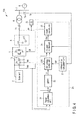
- FIG. 1 is a block diagram showing a constitution of a solar power generation system 10 to which a control apparatus 2 of an inverter 1 according to a first embodiment of the invention is applied. It is to be noted that the same parts as in the drawings are denoted with like reference signs to omit detailed description of the parts, and different parts will mainly be described. Also in the subsequent embodiments, repeated descriptions are similarly omitted.
- the solar power generation system 10 comprises the inverter 1, the control apparatus 2, a solar cell 3, a smoothing capacitor 4, an AC filter 5, an interconnection transformer 6, an AC current detector 71, an overcurrent relay 72, an AC voltage detector 73, and a DC voltage detector 74.
- the solar power generation system 10 is a dispersed generation system which interconnects with an AC power system including a system bus 7 and an AC power source 8.
- the solar cell 3 is a cell which generates power by sunlight energy.
- the solar cell 3 supplies the generated DC power to the inverter 1.
- the inverter 1 is an inverter subjected to pulse width modulation (PWM) control.
- the inverter 1 converts the DC power supplied from the DC power source 3 into the AC power which synchronizes with the AC power source 8.
- the inverter 1 supplies the AC power to the system bus 7 connected to the AC power source 8, via the interconnection transformer 6.
- a power conversion circuit (an inverter circuit) is constituted of a switching element.
- the switching element is driven by a gate signal Gt output from the control apparatus 2. In consequence, the inverter 1 performs the power conversion.
- the smoothing capacitor 4 is disposed on a DC side of the inverter 1.
- the smoothing capacitor 4 smoothes the DC power supplied from the solar cell 3 to the inverter 1.
- the AC filter 5 comprises a reactor 51 and a capacitor 52.
- the AC filter 5 removes a noise output from the inverter 1.
- the AC current detector 71 is a detector to measure an output current Iiv of the inverter 1.
- the AC current detector 71 outputs the detected output current Iiv as a detection signal to the control apparatus 2 and the overcurrent relay 72.
- the overcurrent relay 72 performs a protecting operation, when an instantaneous value of the output current Iiv measured by the AC current detector 71 is in excess of a beforehand setting value.
- the AC voltage detector 73 is a detector to measure a system voltage Vr of the system bus 7.
- the AC voltage detector 73 outputs the detected system voltage Vr as a detection signal to the control apparatus 2.
- the DC voltage detector 74 is a detector to measure a DC voltage Vdc which is to be applied to the DC side of the inverter 1.
- the DC voltage detector 74 outputs the detected DC voltage Vdc as a detection signal to the control apparatus 2.
- a DC current detector 75 is a detector to measure a direct current Idc which is to be input into the DC side of the inverter 1.
- the DC current detector 75 outputs a detected direct current Idc as a detection signal to the control apparatus 2.
- the control apparatus 2 comprises a power calculation unit 21, a maximum power point tracking (MPPT) 22, a DC voltage control unit 23, a current control unit 24, a PWM control unit 25, and a voltage drop detection unit 26.
- MPPT maximum power point tracking
- the power calculation unit 21 calculates a DC power Pdc on the basis of the DC voltage Vdc detected by the DC voltage detector 74 and the direct current Idc detected by the DC current detector 75.
- the power calculation unit 21 outputs the calculated DC power Pdc to the MPPT 22.
- the MPPT 22 outputs, to the DC voltage control unit 23, a voltage increase/decrease signal Vn indicating one of increase and decrease of the DC voltage, on the basis of the DC power Pdc calculated by the power calculation unit 21.
- FIG. 2 is a characteristic diagram showing characteristics of the power generation by the solar cell 3 according to the present embodiment.
- a curve Cvi is a curve indicating a voltage-current correlation in the power generation by the solar cell 3.
- a curve Cp is a curve indicating characteristics of the power in the power generation by the solar cell 3.
- the MPPT 22 performs control to search for a voltage (maximum power point voltage) Vmpp of a maximum power point Pmmp which is the maximum power in the curve Cp shown in FIG. 2 .
- the control is as follows.
- the DC voltage Vdc is controlled to a certain suitable voltage value.
- the MPPT 22 measures the DC power Pdc at this voltage.
- the MPPT 22 outputs the voltage increase/decrease signal Vn to raise (or lower) the DC voltage Vdc as much as a predetermined voltage for one stage.
- the DC voltage is slightly raised (or lowered) by the control of the DC voltage control unit 23.
- the MPPT 22 measures the raised (or lowered) DC power Pdc.
- the MPPT 22 compares the previously measured DC power Pdc with the DC power Pdc newly measured this time.
- the MPPT 22 When the DC power Pdc newly measured this time is larger, the MPPT 22 outputs the voltage increase/decrease signal Vn indicating the same direction as the previous direction. That is, when the previous voltage increase/decrease signal Vn is the signal to raise the voltage, the voltage increase/decrease signal Vn is output as the signal to raise the voltage also this time. When the previous voltage increase/decrease signal Vn is the signal to lower the voltage, the voltage increase/decrease signal Vn is output as the signal to lower the voltage also this time.
- the MPPT 22 When the DC power Pdc newly measured this time is smaller, the MPPT 22 outputs the voltage increase/decrease signal Vn which is different from the previous signal. That is, when the previous voltage increase/decrease signal Vn is the signal to raise the voltage, the voltage increase/decrease signal Vn is output as the signal to lower the voltage this time. When the previous voltage increase/decrease signal Vn is the signal to lower the voltage, the voltage increase/decrease signal Vn is output as the signal to raise the voltage this time.
- the MPPT 22 repeats the above procedure to perform the control so that the DC voltage Vdc is always in the vicinity of the maximum power point voltage Vmpp.
- the system voltage Vr detected by the AC voltage detector 73 is input.
- the voltage drop detection unit 26 outputs a detection signal Sd to the DC voltage control unit 23 on the basis of the system voltage Vr.
- the voltage drop detection unit 26 sets the detection signal Sd to "0", when the system voltage Vr is not less than a predetermined reference voltage (usual time).
- the voltage drop detection unit 26 sets the detection signal Sd to "1", when the system voltage Vr is below the predetermined reference voltage (at the drop of the system voltage Vr).
- the DC voltage control unit 23 there are input the DC voltage Vdc detected by the DC voltage detector 74, the voltage increase/decrease signal Vn output from the MPPT 22, the detection signal Sd output from the voltage drop detection unit 26, and a voltage command value Vivr calculated by the current control unit 24.
- the DC voltage control unit 23 performs the control of the DC voltage Vdc at the usual time by the MPPT 22, when the detection signal Sd is "0".
- the DC voltage control unit 23 performs the control of the DC voltage Vdc at the drop of the system voltage Vr, when the detection signal Sd is "1".
- the DC voltage control unit 23 calculates a DC voltage command value Vdcr to control the DC voltage Vdc.
- the DC voltage control unit 23 outputs the calculated DC voltage command value Vdcr to the current control unit 24.
- the current control unit 24 there are input the output current Iiv detected by the AC current detector 71, the DC power Pdc calculated by the power calculation unit 21, and the DC voltage command value Vdcr calculated by the DC voltage control unit 23.
- the current control unit 24 calculates a voltage command value Vivr to control an output voltage of the inverter 1, on the basis of the output current Iiv, the DC power Pdc, and the DC voltage command value Vdcr.
- the current control unit 24 outputs the calculated voltage command value Vivr to the PWM control unit 25.
- the PWM control unit 25 Into the PWM control unit 25, the voltage command value Vivr calculated by the current control unit 24 is input.
- the PWM control unit 25 generates the gate signal Gt so that the output voltage of the inverter 1 is controlled to the voltage command value Vivr.
- the gate signal Gt drives the switching element of the inverter 1. In consequence, the inverter 1 is subjected to PWM control.
- FIG. 3 is a block diagram showing a constitution of the DC voltage control unit 23 according to the present embodiment.
- the DC voltage control unit 23 comprises a usual time DC voltage control unit 231 and a voltage drop time DC voltage control unit 232.
- the detection signal Sd is "0”
- the DC voltage Vdc is controlled by the usual time DC voltage control unit 231.
- the detection signal Sd is "1”
- the DC voltage Vdc is controlled by the voltage drop time DC voltage control unit 232.
- the usual time DC voltage control unit 231 there are input the DC voltage Vdc detected by the DC voltage detector 74, the voltage increase/decrease signal Vn output from the MPPT 22, and the detection signal Sd output from the voltage drop detection unit 26.
- the usual time DC voltage control unit 231 stops the control. At this time, the usual time DC voltage control unit 231 retains the DC voltage command value Vdcr output just before the stop.
- the usual time DC voltage control unit 231 starts the control. At this time, the DC voltage command value Vdcr retained at the stop of the control is output.
- the usual time DC voltage control unit 231 controls the DC voltage Vdc in accordance with the above-mentioned control by the MPPT 22.
- the voltage drop time DC voltage control unit 232 there are input the DC voltage Vdc detected by the DC voltage detector 74, the detection signal Sd output from the voltage drop detection unit 26, and the voltage command value Vivr calculated by the current control unit 24. On receiving the detection signal Sd indicating "1", the voltage drop time DC voltage control unit 232 starts the control. On receiving the detection signal Sd indicating "0”, the voltage drop time DC voltage control unit 232 stops the control.
- the voltage drop time DC voltage control unit 232 calculates the DC voltage command value Vdcr to raise the DC voltage Vdc so that a ripple of the output current Iiv of the inverter 1 does not exceed the setting value of the overcurrent relay 72, on the basis of the voltage command value Vivr calculated by the current control unit 24. That is, the voltage drop time DC voltage control unit 232 continues to raise the DC voltage Vdc until the output current Iiv of the inverter 1 becomes a value which is not more than a predetermined value. As shown in FIG. 2 , when the DC voltage Vdc is raised in excess of the maximum power point voltage Vmpp, the direct current Idc decreases. After the output current Iiv of the inverter 1 becomes the value which is not more than the predetermined value, the voltage drop time DC voltage control unit 232 maintains the DC voltage Vdc during the drop of the system voltage Vr.
- the control to raise the DC voltage Vdc is performed.
- the direct current Idc to be input into the inverter 1 decreases. Therefore, the output current Iiv of the inverter 1 also decreases. In consequence, it is possible to prevent a false operation of the overcurrent relay 72 due to the ripple of the output current Iiv of the inverter 1.
- the control of the DC voltage Vdc by the MPPT 22 is performed, so that a power generation efficiency of the solar cell 3 can be maximized.
- FIG. 4 is a block diagram showing a constitution of a solar power generation system 10A to which a control apparatus 2A of an inverter 1 according to a second embodiment of the invention is applied.
- the solar power generation system 10A has a constitution where in the solar power generation system 10 according to the first embodiment shown in FIG. 1 , the control apparatus 2 is replaced with the control apparatus 2A.
- the other aspects are similar to those of the solar power generation system 10 according to the first embodiment.
- the control apparatus 2A has a constitution where in the control apparatus 2 according to the first embodiment, the DC voltage control unit 23 is replaced with a DC voltage control unit 23A and the voltage drop detection unit 26 is replaced with a voltage drop calculation unit 27.
- the other aspects are similar to those of the control apparatus 2 according to the first embodiment.
- a system voltage Vr detected by an AC voltage detector 73 is input into the voltage drop calculation unit 27 .
- the voltage drop calculation unit 27 calculates a voltage drop ⁇ V by subtracting the system voltage Vr from a rated voltage.
- the voltage drop calculation unit 27 outputs the calculated voltage drop ⁇ V to the DC voltage control unit 23A.
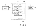
- FIG. 5 is a block diagram showing a constitution of the DC voltage control unit 23A according to the present embodiment.
- the DC voltage control unit 23A has a constitution where in the DC voltage control unit 23 according to the first embodiment shown in FIG. 3 , the voltage drop time DC voltage control unit 232 is replaced with a voltage drop time DC voltage control unit 232A.
- the other aspects are similar to those of the DC voltage control unit 23 according to the first embodiment.
- the time when the detection signal Sd is "0" according to the first embodiment corresponds to a time when the voltage drop ⁇ V is "0" (or a time when the voltage drop ⁇ V is not calculated)
- the time when the detection signal Sd is "1" according to the first embodiment corresponds to a time when the voltage drop ⁇ V is not "0".
- the voltage drop time DC voltage control unit 232A Into the voltage drop time DC voltage control unit 232A, there are input a DC voltage Vdc detected by a DC voltage detector 74 and the voltage drop ⁇ V calculated by the voltage drop calculation unit 27.
- the voltage drop time DC voltage control unit 232A starts control, when the voltage drop ⁇ V is not "0" (at the drop of the system voltage Vr).
- the voltage drop time DC voltage control unit 232A stops the control, when the voltage drop ⁇ V is "0" (usual time).
- the voltage drop time DC voltage control unit 232A calculates a DC voltage command value Vdcr on the basis of the voltage drop ⁇ V.
- the voltage drop time DC voltage control unit 232A performs the calculation so that the larger the voltage drop ⁇ V is, the larger the DC voltage command value Vdcr becomes. That is, the voltage drop time DC voltage control unit 232A noticeably raises the DC voltage Vdc, as the voltage drop ⁇ V increases. In consequence, the voltage drop time DC voltage control unit 232A decreases an output current Iiv of the inverter 1 in accordance with the voltage drop ⁇ V.
- a current ripple to be superimposed on the output current Iiv of the inverter 1 is generated in accordance with the following equation.
- di / dt ⁇ V / L in which the left side is a change ratio of the output current Iiv of the inverter 1.
- L is a reactor component between the inverter 1 and a system bus 7.
- ⁇ V is the voltage drop of the system voltage Vr.
- the DC voltage command value Vdcr is set so that the current ripple predicted in accordance with the above equation is suppressed.
- the control to raise the DC voltage Vdc is performed in accordance with the voltage drop ⁇ V of the system voltage Vr. Therefore, a function and an effect similar to those of the first embodiment can be obtained.
- the DC voltage Vdc of the inverter 1 is raised to suppress the output current Iiv of the inverter 1, but the control may be performed so that the DC voltage Vdc is lowered to suppress the output current Iiv.
- the control to suppress the output current Iiv can be performed. In consequence, a function and an effect similar to those of each embodiment can be obtained.
- an equation to obtain the DC voltage command value Vdcr at the drop of the system voltage Vr may not be based on the above equation (1).
- the equation to obtain the DC voltage command value Vdcr may be obtained by empirical rule or know-how.
- the interconnection transformer 6 interposed between the solar power generation system 10 and the AC power system may not be disposed.
- the voltage detected by the AC voltage detector 73 is an electricity at the same measuring position as that of the current detected by the AC current detector 71.
- a power conversion apparatus to be applied to a generation system which interconnects with an AC power system, so that a false operation of an overcurrent relay disposed on an AC output side can be prevented.
Landscapes
- Engineering & Computer Science (AREA)
- Power Engineering (AREA)
- Life Sciences & Earth Sciences (AREA)
- Sustainable Development (AREA)
- Sustainable Energy (AREA)
- Physics & Mathematics (AREA)
- Electromagnetism (AREA)
- General Physics & Mathematics (AREA)
- Radar, Positioning & Navigation (AREA)
- Automation & Control Theory (AREA)
- Inverter Devices (AREA)
- Control Of Electrical Variables (AREA)
Abstract
Description
- The invention relates to a solar power generation system which interconnects with an alternating current power system.
- In general, an inverter is used in a solar power generation system to interconnect with an alternating current (AC) power system. The inverter converts a direct current (DC) power generated by a solar cell into an AC power which synchronizes with the AC power system, to supply the power to the AC power system. Moreover, on an AC output side of the inverter, an overcurrent relay is disposed to protect the inverter.
- However, the overcurrent relay for use in this way performs the following false operation sometimes. When a system voltage drops owing to a fault or the like of the AC power system, an amplitude of a ripple of an alternating current output from the inverter increases. In consequence, even when an instantaneous value of a current of a fundamental component is not in excess of a setting value at which the overcurrent relay operates, the instantaneous value due to the amplitude of the ripple of the current exceeds the setting value, so that the overcurrent relay operates sometimes. In this case, the overcurrent relay is to bring about a false operation.
-
- Patent Literature 1:
U.S. Patent No. 6921985 - An object of the invention is to provide a solar power generation system which interconnects with an AC power system and which can prevent a false operation of an overcurrent relay disposed on the side of the AC power system.
- In accordance with an aspect of the invention, there is provided a solar power generation system that interconnects with an alternating current power system. The solar power generation system characterized by comprises a solar cell; an inverter that converts a direct current power generated by the solar cell into an alternating current power; system voltage measurement means for measuring a system voltage of the alternating current power system; voltage drop detection means for detecting a voltage drop of the alternating current power system, based on the system voltage measured by the system voltage measurement means; first direct current voltage control means for controlling a direct current voltage of the inverter to enhance a power generation efficiency of the solar cell, when the voltage drop is not detected by the voltage drop detection means; and second direct current voltage control means for controlling the direct current voltage of the inverter to suppress a current output from the inverter, when the voltage drop is detected by the voltage drop detection means.
-
-
FIG. 1 is a block diagram showing a constitution of a solar power generation system to which a control apparatus of an inverter according to a first embodiment of the invention is applied; -
FIG. 2 is a characteristic diagram showing characteristics of power generation by a solar cell according to the first embodiment; -
FIG. 3 is a block diagram showing a constitution of a DC voltage control unit according to the first embodiment; -
FIG. 4 is a block diagram showing a constitution of a solar power generation system to which a control apparatus of an inverter according to a second embodiment of the invention is applied; and -
FIG. 5 is a block diagram showing a constitution of a DC voltage control unit according to the second embodiment. - Mode for Carrying Out the Invention Hereinafter, embodiments of the invention will be described with reference to the drawings.
-
FIG. 1 is a block diagram showing a constitution of a solarpower generation system 10 to which acontrol apparatus 2 of aninverter 1 according to a first embodiment of the invention is applied. It is to be noted that the same parts as in the drawings are denoted with like reference signs to omit detailed description of the parts, and different parts will mainly be described. Also in the subsequent embodiments, repeated descriptions are similarly omitted. - The solar
power generation system 10 comprises theinverter 1, thecontrol apparatus 2, asolar cell 3, asmoothing capacitor 4, anAC filter 5, aninterconnection transformer 6, anAC current detector 71, anovercurrent relay 72, anAC voltage detector 73, and aDC voltage detector 74. The solarpower generation system 10 is a dispersed generation system which interconnects with an AC power system including a system bus 7 and anAC power source 8. - The
solar cell 3 is a cell which generates power by sunlight energy. Thesolar cell 3 supplies the generated DC power to theinverter 1. - The
inverter 1 is an inverter subjected to pulse width modulation (PWM) control. Theinverter 1 converts the DC power supplied from theDC power source 3 into the AC power which synchronizes with theAC power source 8. Theinverter 1 supplies the AC power to the system bus 7 connected to theAC power source 8, via theinterconnection transformer 6. In theinverter 1, a power conversion circuit (an inverter circuit) is constituted of a switching element. The switching element is driven by a gate signal Gt output from thecontrol apparatus 2. In consequence, theinverter 1 performs the power conversion. - The
smoothing capacitor 4 is disposed on a DC side of theinverter 1. Thesmoothing capacitor 4 smoothes the DC power supplied from thesolar cell 3 to theinverter 1. - The
AC filter 5 comprises areactor 51 and acapacitor 52. TheAC filter 5 removes a noise output from theinverter 1. - The AC
current detector 71 is a detector to measure an output current Iiv of theinverter 1. The ACcurrent detector 71 outputs the detected output current Iiv as a detection signal to thecontrol apparatus 2 and theovercurrent relay 72. - The
overcurrent relay 72 performs a protecting operation, when an instantaneous value of the output current Iiv measured by the ACcurrent detector 71 is in excess of a beforehand setting value. - The
AC voltage detector 73 is a detector to measure a system voltage Vr of the system bus 7. TheAC voltage detector 73 outputs the detected system voltage Vr as a detection signal to thecontrol apparatus 2. - The
DC voltage detector 74 is a detector to measure a DC voltage Vdc which is to be applied to the DC side of theinverter 1. TheDC voltage detector 74 outputs the detected DC voltage Vdc as a detection signal to thecontrol apparatus 2. - A
DC current detector 75 is a detector to measure a direct current Idc which is to be input into the DC side of theinverter 1. The DCcurrent detector 75 outputs a detected direct current Idc as a detection signal to thecontrol apparatus 2. - The
control apparatus 2 comprises apower calculation unit 21, a maximum power point tracking (MPPT) 22, a DCvoltage control unit 23, acurrent control unit 24, aPWM control unit 25, and a voltagedrop detection unit 26. - The
power calculation unit 21 calculates a DC power Pdc on the basis of the DC voltage Vdc detected by theDC voltage detector 74 and the direct current Idc detected by theDC current detector 75. Thepower calculation unit 21 outputs the calculated DC power Pdc to theMPPT 22. - The
MPPT 22 outputs, to the DCvoltage control unit 23, a voltage increase/decrease signal Vn indicating one of increase and decrease of the DC voltage, on the basis of the DC power Pdc calculated by thepower calculation unit 21. - Control of the DC voltage Vdc by the
MPPT 22 will be described with reference toFIG. 2. FIG. 2 is a characteristic diagram showing characteristics of the power generation by thesolar cell 3 according to the present embodiment. A curve Cvi is a curve indicating a voltage-current correlation in the power generation by thesolar cell 3. A curve Cp is a curve indicating characteristics of the power in the power generation by thesolar cell 3. - The
MPPT 22 performs control to search for a voltage (maximum power point voltage) Vmpp of a maximum power point Pmmp which is the maximum power in the curve Cp shown inFIG. 2 . Specifically, the control is as follows. - First, the DC voltage Vdc is controlled to a certain suitable voltage value. The
MPPT 22 measures the DC power Pdc at this voltage. - Next, the
MPPT 22 outputs the voltage increase/decrease signal Vn to raise (or lower) the DC voltage Vdc as much as a predetermined voltage for one stage. In consequence, the DC voltage is slightly raised (or lowered) by the control of the DCvoltage control unit 23. - The
MPPT 22 measures the raised (or lowered) DC power Pdc. TheMPPT 22 compares the previously measured DC power Pdc with the DC power Pdc newly measured this time. - When the DC power Pdc newly measured this time is larger, the
MPPT 22 outputs the voltage increase/decrease signal Vn indicating the same direction as the previous direction. That is, when the previous voltage increase/decrease signal Vn is the signal to raise the voltage, the voltage increase/decrease signal Vn is output as the signal to raise the voltage also this time. When the previous voltage increase/decrease signal Vn is the signal to lower the voltage, the voltage increase/decrease signal Vn is output as the signal to lower the voltage also this time. - When the DC power Pdc newly measured this time is smaller, the
MPPT 22 outputs the voltage increase/decrease signal Vn which is different from the previous signal. That is, when the previous voltage increase/decrease signal Vn is the signal to raise the voltage, the voltage increase/decrease signal Vn is output as the signal to lower the voltage this time. When the previous voltage increase/decrease signal Vn is the signal to lower the voltage, the voltage increase/decrease signal Vn is output as the signal to raise the voltage this time. - The
MPPT 22 repeats the above procedure to perform the control so that the DC voltage Vdc is always in the vicinity of the maximum power point voltage Vmpp. - Into the voltage
drop detection unit 26, the system voltage Vr detected by theAC voltage detector 73 is input. The voltagedrop detection unit 26 outputs a detection signal Sd to the DCvoltage control unit 23 on the basis of the system voltage Vr. The voltagedrop detection unit 26 sets the detection signal Sd to "0", when the system voltage Vr is not less than a predetermined reference voltage (usual time). The voltagedrop detection unit 26 sets the detection signal Sd to "1", when the system voltage Vr is below the predetermined reference voltage (at the drop of the system voltage Vr). - Into the DC
voltage control unit 23, there are input the DC voltage Vdc detected by theDC voltage detector 74, the voltage increase/decrease signal Vn output from theMPPT 22, the detection signal Sd output from the voltagedrop detection unit 26, and a voltage command value Vivr calculated by thecurrent control unit 24. The DCvoltage control unit 23 performs the control of the DC voltage Vdc at the usual time by theMPPT 22, when the detection signal Sd is "0". The DCvoltage control unit 23 performs the control of the DC voltage Vdc at the drop of the system voltage Vr, when the detection signal Sd is "1". The DCvoltage control unit 23 calculates a DC voltage command value Vdcr to control the DC voltage Vdc. The DCvoltage control unit 23 outputs the calculated DC voltage command value Vdcr to thecurrent control unit 24. - Into the
current control unit 24, there are input the output current Iiv detected by the ACcurrent detector 71, the DC power Pdc calculated by thepower calculation unit 21, and the DC voltage command value Vdcr calculated by the DCvoltage control unit 23. Thecurrent control unit 24 calculates a voltage command value Vivr to control an output voltage of theinverter 1, on the basis of the output current Iiv, the DC power Pdc, and the DC voltage command value Vdcr. Thecurrent control unit 24 outputs the calculated voltage command value Vivr to thePWM control unit 25. - Into the
PWM control unit 25, the voltage command value Vivr calculated by thecurrent control unit 24 is input. ThePWM control unit 25 generates the gate signal Gt so that the output voltage of theinverter 1 is controlled to the voltage command value Vivr. The gate signal Gt drives the switching element of theinverter 1. In consequence, theinverter 1 is subjected to PWM control. -
FIG. 3 is a block diagram showing a constitution of the DCvoltage control unit 23 according to the present embodiment. - The DC
voltage control unit 23 comprises a usual time DCvoltage control unit 231 and a voltage drop time DCvoltage control unit 232. When the detection signal Sd is "0", the DC voltage Vdc is controlled by the usual time DCvoltage control unit 231. When the detection signal Sd is "1", the DC voltage Vdc is controlled by the voltage drop time DCvoltage control unit 232. - Into the usual time DC
voltage control unit 231, there are input the DC voltage Vdc detected by theDC voltage detector 74, the voltage increase/decrease signal Vn output from theMPPT 22, and the detection signal Sd output from the voltagedrop detection unit 26. On receiving the detection signal Sd indicating "1", the usual time DCvoltage control unit 231 stops the control. At this time, the usual time DCvoltage control unit 231 retains the DC voltage command value Vdcr output just before the stop. On receiving the detection signal Sd indicating "0", the usual time DCvoltage control unit 231 starts the control. At this time, the DC voltage command value Vdcr retained at the stop of the control is output. Afterward, the usual time DCvoltage control unit 231 controls the DC voltage Vdc in accordance with the above-mentioned control by theMPPT 22. - Into the voltage drop time DC
voltage control unit 232, there are input the DC voltage Vdc detected by theDC voltage detector 74, the detection signal Sd output from the voltagedrop detection unit 26, and the voltage command value Vivr calculated by thecurrent control unit 24. On receiving the detection signal Sd indicating "1", the voltage drop time DCvoltage control unit 232 starts the control. On receiving the detection signal Sd indicating "0", the voltage drop time DCvoltage control unit 232 stops the control. - The voltage drop time DC
voltage control unit 232 calculates the DC voltage command value Vdcr to raise the DC voltage Vdc so that a ripple of the output current Iiv of theinverter 1 does not exceed the setting value of theovercurrent relay 72, on the basis of the voltage command value Vivr calculated by thecurrent control unit 24. That is, the voltage drop time DCvoltage control unit 232 continues to raise the DC voltage Vdc until the output current Iiv of theinverter 1 becomes a value which is not more than a predetermined value. As shown inFIG. 2 , when the DC voltage Vdc is raised in excess of the maximum power point voltage Vmpp, the direct current Idc decreases. After the output current Iiv of theinverter 1 becomes the value which is not more than the predetermined value, the voltage drop time DCvoltage control unit 232 maintains the DC voltage Vdc during the drop of the system voltage Vr. - According to the present embodiment, when the system voltage Vr of the interconnecting power system drops, the control to raise the DC voltage Vdc is performed. In consequence, the direct current Idc to be input into the
inverter 1 decreases. Therefore, the output current Iiv of theinverter 1 also decreases. In consequence, it is possible to prevent a false operation of theovercurrent relay 72 due to the ripple of the output current Iiv of theinverter 1. Moreover, at the usual time, the control of the DC voltage Vdc by theMPPT 22 is performed, so that a power generation efficiency of thesolar cell 3 can be maximized. -
FIG. 4 is a block diagram showing a constitution of a solarpower generation system 10A to which acontrol apparatus 2A of aninverter 1 according to a second embodiment of the invention is applied. - The solar
power generation system 10A has a constitution where in the solarpower generation system 10 according to the first embodiment shown inFIG. 1 , thecontrol apparatus 2 is replaced with thecontrol apparatus 2A. The other aspects are similar to those of the solarpower generation system 10 according to the first embodiment. - The
control apparatus 2A has a constitution where in thecontrol apparatus 2 according to the first embodiment, the DCvoltage control unit 23 is replaced with a DCvoltage control unit 23A and the voltagedrop detection unit 26 is replaced with a voltagedrop calculation unit 27. The other aspects are similar to those of thecontrol apparatus 2 according to the first embodiment. - Into the voltage
drop calculation unit 27, a system voltage Vr detected by anAC voltage detector 73 is input. When the system voltage Vr is below a predetermined reference voltage (at the drop of the system voltage Vr), the voltagedrop calculation unit 27 calculates a voltage drop ΔV by subtracting the system voltage Vr from a rated voltage. The voltagedrop calculation unit 27 outputs the calculated voltage drop ΔV to the DCvoltage control unit 23A. -
FIG. 5 is a block diagram showing a constitution of the DCvoltage control unit 23A according to the present embodiment. - The DC
voltage control unit 23A has a constitution where in the DCvoltage control unit 23 according to the first embodiment shown inFIG. 3 , the voltage drop time DCvoltage control unit 232 is replaced with a voltage drop time DCvoltage control unit 232A. The other aspects are similar to those of the DCvoltage control unit 23 according to the first embodiment. It is to be noted that in a usual time DCvoltage control unit 231 according to the present embodiment, the time when the detection signal Sd is "0" according to the first embodiment corresponds to a time when the voltage drop ΔV is "0" (or a time when the voltage drop ΔV is not calculated), and the time when the detection signal Sd is "1" according to the first embodiment corresponds to a time when the voltage drop ΔV is not "0". - Into the voltage drop time DC
voltage control unit 232A, there are input a DC voltage Vdc detected by aDC voltage detector 74 and the voltage drop ΔV calculated by the voltagedrop calculation unit 27. The voltage drop time DCvoltage control unit 232A starts control, when the voltage drop ΔV is not "0" (at the drop of the system voltage Vr). The voltage drop time DCvoltage control unit 232A stops the control, when the voltage drop ΔV is "0" (usual time). - At the drop of the system voltage Vr, the voltage drop time DC
voltage control unit 232A calculates a DC voltage command value Vdcr on the basis of the voltage drop ΔV. The voltage drop time DCvoltage control unit 232A performs the calculation so that the larger the voltage drop ΔV is, the larger the DC voltage command value Vdcr becomes. That is, the voltage drop time DCvoltage control unit 232A noticeably raises the DC voltage Vdc, as the voltage drop ΔV increases. In consequence, the voltage drop time DCvoltage control unit 232A decreases an output current Iiv of theinverter 1 in accordance with the voltage drop ΔV. - Next, a calculation method of the DC voltage command value Vdcr at the drop of the system voltage Vr will be described.
- A current ripple to be superimposed on the output current Iiv of the
inverter 1 is generated in accordance with the following equation.
in which the left side is a change ratio of the output current Iiv of theinverter 1. L is a reactor component between theinverter 1 and a system bus 7. ΔV is the voltage drop of the system voltage Vr. - The DC voltage command value Vdcr is set so that the current ripple predicted in accordance with the above equation is suppressed.
- According to the present embodiment, the control to raise the DC voltage Vdc is performed in accordance with the voltage drop ΔV of the system voltage Vr. Therefore, a function and an effect similar to those of the first embodiment can be obtained.
- It is to be noted that in the respective embodiments, the DC voltage Vdc of the
inverter 1 is raised to suppress the output current Iiv of theinverter 1, but the control may be performed so that the DC voltage Vdc is lowered to suppress the output current Iiv. When the DC voltage Vdc is controlled so that the maximum power point voltage Vmpp shown inFIG. 2 is excluded, the control to suppress the output current Iiv can be performed. In consequence, a function and an effect similar to those of each embodiment can be obtained. - Moreover, in the second embodiment, an equation to obtain the DC voltage command value Vdcr at the drop of the system voltage Vr may not be based on the above equation (1). For example, the equation to obtain the DC voltage command value Vdcr may be obtained by empirical rule or know-how.
- Furthermore, in the respective embodiments, the
interconnection transformer 6 interposed between the solarpower generation system 10 and the AC power system may not be disposed. In this case, the voltage detected by theAC voltage detector 73 is an electricity at the same measuring position as that of the current detected by the ACcurrent detector 71. - It is to be noted that the present invention is not restricted to the foregoing embodiments, and constituent elements can be modified and changed into shapes without departing from the scope of the invention at an embodying stage. Additionally, various inventions can be formed by appropriately combining a plurality of constituent elements disclosed in the foregoing embodiments. For example, several constituent elements may be eliminated from all constituent elements disclosed in the embodiments. Furthermore, constituent elements in the different embodiments may be appropriately combined.
- According to the invention, there can be provided a power conversion apparatus to be applied to a generation system which interconnects with an AC power system, so that a false operation of an overcurrent relay disposed on an AC output side can be prevented.
Claims (15)
- A solar power generation system that interconnects with an alternating current power system, the solar power generation system characterized by comprising:a solar cell;an inverter that converts a direct current power generated by the solar cell into an alternating current power;system voltage measurement means for measuring a system voltage of the alternating current power system;voltage drop detection means for detecting a voltage drop of the alternating current power system, based on the system voltage measured by the system voltage measurement means;first direct current voltage control means for controlling a direct current voltage of the inverter to enhance a power generation efficiency of the solar cell, when the voltage drop is not detected by the voltage drop detection means; andsecond direct current voltage control means for controlling the direct current voltage of the inverter to suppress a current output from the inverter, when the voltage drop is detected by the voltage drop detection means.
- The solar power generation system according to claim 1, characterized in that the second direct current voltage control means performs control to raise the direct current voltage of the inverter, when the voltage drop is detected by the voltage drop detection means.
- The solar power generation system according to claim 2, characterized in that the second direct current voltage control means changes a voltage to raise the direct current voltage of the inverter in accordance with the voltage drop, when the voltage drop is detected by the voltage drop detection means.
- The solar power generation system according to claim 1, characterized in that the second direct current voltage control means performs control to lower the direct current voltage of the inverter, when the voltage drop is detected by the voltage drop detection means.
- The solar power generation system according to claim 4, characterized in that the second direct current voltage control means changes a voltage to lower the direct current voltage of the inverter in accordance with the voltage drop, when the voltage drop is detected by the voltage drop detection means.
- A control apparatus for an inverter that controls the inverter to be applied to a solar power generation system interconnecting with an alternating current power system and including a solar cell, the control apparatus characterized by comprising:system voltage measurement means for measuring a system voltage of the alternating current power system;voltage drop detection means for detecting a voltage drop of the alternating current power system, based on the system voltage measured by the system voltage measurement means;first direct current voltage control means for controlling a direct current voltage of the inverter to enhance a power generation efficiency of the solar cell, when the voltage drop is not detected by the voltage drop detection means; andsecond direct current voltage control means for controlling the direct current voltage of the inverter to suppress a current output from the inverter, when the voltage drop is detected by the voltage drop detection means.
- The control apparatus for the inverter according to claim 6, characterized in that the second direct current voltage control means performs control to raise the direct current voltage of the inverter, when the voltage drop is detected by the voltage drop detection means.
- The control apparatus for the inverter according to claim 7, characterized in that the second direct current voltage control means changes a voltage to raise the direct current voltage of the inverter in accordance with the voltage drop, when the voltage drop is detected by the voltage drop detection means.
- The control apparatus for the inverter according to claim 6, characterized in that the second direct current voltage control means performs control to lower the direct current voltage of the inverter, when the voltage drop is detected by the voltage drop detection means.
- The control apparatus for the inverter according to claim 9, characterized in that the second direct current voltage control means changes a voltage to lower the direct current voltage of the inverter in accordance with the voltage drop, when the voltage drop is detected by the voltage drop detection means.
- A control method for an inverter that controls the inverter to be applied to a solar power generation system interconnecting with an alternating current power system and including a solar cell, the control method characterized by comprising:measuring a system voltage of the alternating current power system;detecting a voltage drop of the alternating current power system, based on the measured system voltage;controlling a direct current voltage of the inverter to enhance a power generation efficiency of the solar cell, when the voltage drop of the alternating current power system is not detected; andcontrolling the direct current voltage of the inverter to suppress a current output from the inverter, when the voltage drop of the alternating current power system is detected.
- The control method for the inverter according to claim 11, characterized in that when the voltage drop of the alternating current power system is detected, control is performed to raise the direct current voltage of the inverter.
- The control method for the inverter according to claim 12, characterized in that when the voltage drop of the alternating current power system is detected, a voltage to raise the direct current voltage of the inverter is changed in accordance with the voltage drop.
- The control method for the inverter according to claim 11, characterized in that when the voltage drop of the alternating current power system is detected, control to lower the direct current voltage of the inverter is performed.
- The control method for the inverter according to claim 14, characterized in that when the voltage drop of the alternating current power system is detected, a voltage to lower the direct current voltage of the inverter is changed in accordance with the voltage drop.
Applications Claiming Priority (1)
| Application Number | Priority Date | Filing Date | Title |
|---|---|---|---|
| PCT/JP2011/053958 WO2012114469A1 (en) | 2011-02-23 | 2011-02-23 | Solar power generation system |
Publications (3)
| Publication Number | Publication Date |
|---|---|
| EP2680426A1 true EP2680426A1 (en) | 2014-01-01 |
| EP2680426A4 EP2680426A4 (en) | 2017-11-22 |
| EP2680426B1 EP2680426B1 (en) | 2021-07-21 |
Family
ID=46720288
Family Applications (1)
| Application Number | Title | Priority Date | Filing Date |
|---|---|---|---|
| EP11859348.2A Active EP2680426B1 (en) | 2011-02-23 | 2011-02-23 | Solar power generation system |
Country Status (6)
| Country | Link |
|---|---|
| US (1) | US9300226B2 (en) |
| EP (1) | EP2680426B1 (en) |
| JP (1) | JP5659290B2 (en) |
| CN (1) | CN103392292B (en) |
| ES (1) | ES2893307T3 (en) |
| WO (1) | WO2012114469A1 (en) |
Cited By (2)
| Publication number | Priority date | Publication date | Assignee | Title |
|---|---|---|---|---|
| EP2922193A1 (en) * | 2014-03-20 | 2015-09-23 | Panasonic Intellectual Property Management Co., Ltd. | Power conversion apparatus and control method for power conversion apparatus |
| EP3176939A4 (en) * | 2014-07-30 | 2018-03-07 | Hitachi Industrial Equipment Systems Co., Ltd. | Power conversion control device and solar power generation system |
Families Citing this family (4)
| Publication number | Priority date | Publication date | Assignee | Title |
|---|---|---|---|---|
| EP3059653B1 (en) * | 2013-10-15 | 2020-11-25 | Toshiba Mitsubishi-Electric Industrial Systems Corporation | Power conversion device and method for controlling same |
| WO2015092918A1 (en) | 2013-12-20 | 2015-06-25 | 東芝三菱電機産業システム株式会社 | Inverter control device |
| JP6153144B1 (en) * | 2016-03-17 | 2017-06-28 | 三菱電機株式会社 | Control device and control method for DC / DC converter |
| WO2022074803A1 (en) * | 2020-10-08 | 2022-04-14 | 東芝三菱電機産業システム株式会社 | Power conversion device |
Family Cites Families (16)
| Publication number | Priority date | Publication date | Assignee | Title |
|---|---|---|---|---|
| JP2736102B2 (en) * | 1989-02-17 | 1998-04-02 | 株式会社東芝 | Control device of power converter for grid connection |
| JP2001136664A (en) * | 1999-11-05 | 2001-05-18 | Hitachi Ltd | Distributed power generation system |
| CN1334985A (en) * | 1999-11-29 | 2002-02-06 | 三菱电机株式会社 | Inverter controller |
| JP2002165357A (en) * | 2000-11-27 | 2002-06-07 | Canon Inc | Power conversion device, control method therefor, and power generation system |
| US6921985B2 (en) | 2003-01-24 | 2005-07-26 | General Electric Company | Low voltage ride through for wind turbine generators |
| JP3980515B2 (en) * | 2003-04-22 | 2007-09-26 | 三菱電機株式会社 | Voltage fluctuation compensation device |
| US7193872B2 (en) * | 2005-01-28 | 2007-03-20 | Kasemsan Siri | Solar array inverter with maximum power tracking |
| US8405367B2 (en) * | 2006-01-13 | 2013-03-26 | Enecsys Limited | Power conditioning units |
| JP2008059968A (en) * | 2006-09-01 | 2008-03-13 | Matsushita Electric Ind Co Ltd | Fuel cell system |
| JP2008228494A (en) * | 2007-03-14 | 2008-09-25 | Kansai Electric Power Co Inc:The | Inverter for coordinating system |
| JP4896044B2 (en) * | 2008-01-07 | 2012-03-14 | 三菱電機株式会社 | Power converter |
| CN101304221B (en) * | 2008-06-19 | 2011-09-28 | 江苏津恒能源科技有限公司 | Solar photovoltaic interconnected inverter |
| EP2443666A4 (en) * | 2009-06-15 | 2013-06-05 | Tenksolar Inc | SOLAR PANEL INDEPENDENT OF LIGHTING |
| US8228697B2 (en) * | 2009-07-20 | 2012-07-24 | General Electric Company | Systems, methods, and apparatus for operating a power converter |
| CN102082443B (en) * | 2009-11-27 | 2013-10-02 | 通用电气公司 | Direct current (DC)-alternating current (AC) converting system and method |
| CN101777775A (en) * | 2010-02-26 | 2010-07-14 | 东南大学 | High-frequency isolation single-phase photovoltaic grid-connected system and control method thereof |
-
2011
- 2011-02-23 WO PCT/JP2011/053958 patent/WO2012114469A1/en not_active Ceased
- 2011-02-23 CN CN201180068310.1A patent/CN103392292B/en active Active
- 2011-02-23 ES ES11859348T patent/ES2893307T3/en active Active
- 2011-02-23 EP EP11859348.2A patent/EP2680426B1/en active Active
- 2011-02-23 JP JP2013500765A patent/JP5659290B2/en active Active
-
2013
- 2013-08-22 US US13/973,641 patent/US9300226B2/en active Active
Non-Patent Citations (1)
| Title |
|---|
| See references of WO2012114469A1 * |
Cited By (3)
| Publication number | Priority date | Publication date | Assignee | Title |
|---|---|---|---|---|
| EP2922193A1 (en) * | 2014-03-20 | 2015-09-23 | Panasonic Intellectual Property Management Co., Ltd. | Power conversion apparatus and control method for power conversion apparatus |
| US9748866B2 (en) | 2014-03-20 | 2017-08-29 | Panasonic Intellectual Property Management Co., Ltd. | Power conversion apparatus and control method for power conversion apparatus when an instantaneous voltage drop has occurred in a power system |
| EP3176939A4 (en) * | 2014-07-30 | 2018-03-07 | Hitachi Industrial Equipment Systems Co., Ltd. | Power conversion control device and solar power generation system |
Also Published As
| Publication number | Publication date |
|---|---|
| WO2012114469A1 (en) | 2012-08-30 |
| EP2680426A4 (en) | 2017-11-22 |
| JP5659290B2 (en) | 2015-01-28 |
| US9300226B2 (en) | 2016-03-29 |
| ES2893307T3 (en) | 2022-02-08 |
| US20130336030A1 (en) | 2013-12-19 |
| CN103392292A (en) | 2013-11-13 |
| CN103392292B (en) | 2016-02-10 |
| EP2680426B1 (en) | 2021-07-21 |
| JPWO2012114469A1 (en) | 2014-07-07 |
Similar Documents
| Publication | Publication Date | Title |
|---|---|---|
| US8988906B2 (en) | Power conversion apparatus | |
| US9673733B2 (en) | Control apparatus for photovoltaic inverter | |
| US9337750B2 (en) | Power conversion apparatus | |
| US9300226B2 (en) | Solar power generation system | |
| WO2012014182A1 (en) | Method and device for maximizing the electrical power produced by a generator, particularly a generator based on a renewable power source | |
| JP6366083B2 (en) | Inverter control device | |
| KR20130049095A (en) | Photovoltaic power generating apparatus and controlling method of the same in grid-connected system | |
| EP3185407A1 (en) | Dc/ac converter with lvrt control | |
| EP3086457B1 (en) | Inverter control device | |
| Varjasi et al. | Sensorless control of a grid-connected pv converter | |
| JP5294908B2 (en) | Power converter |
Legal Events
| Date | Code | Title | Description |
|---|---|---|---|
| PUAI | Public reference made under article 153(3) epc to a published international application that has entered the european phase |
Free format text: ORIGINAL CODE: 0009012 |
|
| 17P | Request for examination filed |
Effective date: 20130821 |
|
| AK | Designated contracting states |
Kind code of ref document: A1 Designated state(s): AL AT BE BG CH CY CZ DE DK EE ES FI FR GB GR HR HU IE IS IT LI LT LU LV MC MK MT NL NO PL PT RO RS SE SI SK SM TR |
|
| DAX | Request for extension of the european patent (deleted) | ||
| RA4 | Supplementary search report drawn up and despatched (corrected) |
Effective date: 20171020 |
|
| RIC1 | Information provided on ipc code assigned before grant |
Ipc: H02M 1/14 20060101ALN20171016BHEP Ipc: H02M 1/32 20070101ALI20171016BHEP Ipc: G05F 1/67 20060101ALN20171016BHEP Ipc: H02J 3/38 20060101AFI20171016BHEP Ipc: H02M 7/5395 20060101ALI20171016BHEP Ipc: H02M 7/539 20060101ALI20171016BHEP |
|
| STAA | Information on the status of an ep patent application or granted ep patent |
Free format text: STATUS: EXAMINATION IS IN PROGRESS |
|
| 17Q | First examination report despatched |
Effective date: 20191115 |
|
| RIC1 | Information provided on ipc code assigned before grant |
Ipc: H02M 1/14 20060101ALN20200812BHEP Ipc: H02M 1/32 20070101ALI20200812BHEP Ipc: H02M 7/539 20060101ALI20200812BHEP Ipc: H02M 7/5395 20060101ALI20200812BHEP Ipc: G05F 1/67 20060101ALN20200812BHEP Ipc: H02J 3/38 20060101AFI20200812BHEP |
|
| GRAP | Despatch of communication of intention to grant a patent |
Free format text: ORIGINAL CODE: EPIDOSNIGR1 |
|
| STAA | Information on the status of an ep patent application or granted ep patent |
Free format text: STATUS: GRANT OF PATENT IS INTENDED |
|
| RIC1 | Information provided on ipc code assigned before grant |
Ipc: H02M 7/539 20060101ALI20200915BHEP Ipc: H02M 1/32 20070101ALI20200915BHEP Ipc: H02M 1/14 20060101ALN20200915BHEP Ipc: H02M 7/5395 20060101ALI20200915BHEP Ipc: H02J 3/38 20060101AFI20200915BHEP Ipc: G05F 1/67 20060101ALN20200915BHEP |
|
| INTG | Intention to grant announced |
Effective date: 20200930 |
|
| GRAJ | Information related to disapproval of communication of intention to grant by the applicant or resumption of examination proceedings by the epo deleted |
Free format text: ORIGINAL CODE: EPIDOSDIGR1 |
|
| STAA | Information on the status of an ep patent application or granted ep patent |
Free format text: STATUS: EXAMINATION IS IN PROGRESS |
|
| REG | Reference to a national code |
Ref country code: DE Ref legal event code: R079 Ref document number: 602011071428 Country of ref document: DE Free format text: PREVIOUS MAIN CLASS: H02M0007480000 Ipc: H02J0003380000 |
|
| GRAS | Grant fee paid |
Free format text: ORIGINAL CODE: EPIDOSNIGR3 |
|
| STAA | Information on the status of an ep patent application or granted ep patent |
Free format text: STATUS: GRANT OF PATENT IS INTENDED |
|
| GRAP | Despatch of communication of intention to grant a patent |
Free format text: ORIGINAL CODE: EPIDOSNIGR1 |
|
| INTC | Intention to grant announced (deleted) | ||
| RAP1 | Party data changed (applicant data changed or rights of an application transferred) |
Owner name: TOSHIBA MITSUBISHI-ELECTRIC INDUSTRIAL SYSTEMS CORPORATION |
|
| RIC1 | Information provided on ipc code assigned before grant |
Ipc: H02M 7/539 20060101ALI20210126BHEP Ipc: H02J 3/38 20060101AFI20210126BHEP Ipc: G05F 1/67 20060101ALN20210126BHEP Ipc: H02M 7/5395 20060101ALI20210126BHEP Ipc: H02M 1/14 20060101ALN20210126BHEP Ipc: H02M 1/32 20070101ALI20210126BHEP |
|
| INTG | Intention to grant announced |
Effective date: 20210212 |
|
| GRAA | (expected) grant |
Free format text: ORIGINAL CODE: 0009210 |
|
| STAA | Information on the status of an ep patent application or granted ep patent |
Free format text: STATUS: THE PATENT HAS BEEN GRANTED |
|
| AK | Designated contracting states |
Kind code of ref document: B1 Designated state(s): AL AT BE BG CH CY CZ DE DK EE ES FI FR GB GR HR HU IE IS IT LI LT LU LV MC MK MT NL NO PL PT RO RS SE SI SK SM TR |
|
| REG | Reference to a national code |
Ref country code: GB Ref legal event code: FG4D |
|
| REG | Reference to a national code |
Ref country code: CH Ref legal event code: EP |
|
| REG | Reference to a national code |
Ref country code: DE Ref legal event code: R096 Ref document number: 602011071428 Country of ref document: DE |
|
| REG | Reference to a national code |
Ref country code: AT Ref legal event code: REF Ref document number: 1413496 Country of ref document: AT Kind code of ref document: T Effective date: 20210815 |
|
| REG | Reference to a national code |
Ref country code: IE Ref legal event code: FG4D |
|
| REG | Reference to a national code |
Ref country code: LT Ref legal event code: MG9D |
|
| REG | Reference to a national code |
Ref country code: NL Ref legal event code: MP Effective date: 20210721 |
|
| REG | Reference to a national code |
Ref country code: AT Ref legal event code: MK05 Ref document number: 1413496 Country of ref document: AT Kind code of ref document: T Effective date: 20210721 |
|
| PG25 | Lapsed in a contracting state [announced via postgrant information from national office to epo] |
Ref country code: HR Free format text: LAPSE BECAUSE OF FAILURE TO SUBMIT A TRANSLATION OF THE DESCRIPTION OR TO PAY THE FEE WITHIN THE PRESCRIBED TIME-LIMIT Effective date: 20210721 Ref country code: SE Free format text: LAPSE BECAUSE OF FAILURE TO SUBMIT A TRANSLATION OF THE DESCRIPTION OR TO PAY THE FEE WITHIN THE PRESCRIBED TIME-LIMIT Effective date: 20210721 Ref country code: BG Free format text: LAPSE BECAUSE OF FAILURE TO SUBMIT A TRANSLATION OF THE DESCRIPTION OR TO PAY THE FEE WITHIN THE PRESCRIBED TIME-LIMIT Effective date: 20211021 Ref country code: AT Free format text: LAPSE BECAUSE OF FAILURE TO SUBMIT A TRANSLATION OF THE DESCRIPTION OR TO PAY THE FEE WITHIN THE PRESCRIBED TIME-LIMIT Effective date: 20210721 Ref country code: LT Free format text: LAPSE BECAUSE OF FAILURE TO SUBMIT A TRANSLATION OF THE DESCRIPTION OR TO PAY THE FEE WITHIN THE PRESCRIBED TIME-LIMIT Effective date: 20210721 Ref country code: RS Free format text: LAPSE BECAUSE OF FAILURE TO SUBMIT A TRANSLATION OF THE DESCRIPTION OR TO PAY THE FEE WITHIN THE PRESCRIBED TIME-LIMIT Effective date: 20210721 Ref country code: NO Free format text: LAPSE BECAUSE OF FAILURE TO SUBMIT A TRANSLATION OF THE DESCRIPTION OR TO PAY THE FEE WITHIN THE PRESCRIBED TIME-LIMIT Effective date: 20211021 Ref country code: NL Free format text: LAPSE BECAUSE OF FAILURE TO SUBMIT A TRANSLATION OF THE DESCRIPTION OR TO PAY THE FEE WITHIN THE PRESCRIBED TIME-LIMIT Effective date: 20210721 Ref country code: PT Free format text: LAPSE BECAUSE OF FAILURE TO SUBMIT A TRANSLATION OF THE DESCRIPTION OR TO PAY THE FEE WITHIN THE PRESCRIBED TIME-LIMIT Effective date: 20211122 Ref country code: FI Free format text: LAPSE BECAUSE OF FAILURE TO SUBMIT A TRANSLATION OF THE DESCRIPTION OR TO PAY THE FEE WITHIN THE PRESCRIBED TIME-LIMIT Effective date: 20210721 |
|
| REG | Reference to a national code |
Ref country code: ES Ref legal event code: FG2A Ref document number: 2893307 Country of ref document: ES Kind code of ref document: T3 Effective date: 20220208 |
|
| PG25 | Lapsed in a contracting state [announced via postgrant information from national office to epo] |
Ref country code: PL Free format text: LAPSE BECAUSE OF FAILURE TO SUBMIT A TRANSLATION OF THE DESCRIPTION OR TO PAY THE FEE WITHIN THE PRESCRIBED TIME-LIMIT Effective date: 20210721 Ref country code: LV Free format text: LAPSE BECAUSE OF FAILURE TO SUBMIT A TRANSLATION OF THE DESCRIPTION OR TO PAY THE FEE WITHIN THE PRESCRIBED TIME-LIMIT Effective date: 20210721 Ref country code: GR Free format text: LAPSE BECAUSE OF FAILURE TO SUBMIT A TRANSLATION OF THE DESCRIPTION OR TO PAY THE FEE WITHIN THE PRESCRIBED TIME-LIMIT Effective date: 20211022 |
|
| REG | Reference to a national code |
Ref country code: DE Ref legal event code: R097 Ref document number: 602011071428 Country of ref document: DE |
|
| PG25 | Lapsed in a contracting state [announced via postgrant information from national office to epo] |
Ref country code: DK Free format text: LAPSE BECAUSE OF FAILURE TO SUBMIT A TRANSLATION OF THE DESCRIPTION OR TO PAY THE FEE WITHIN THE PRESCRIBED TIME-LIMIT Effective date: 20210721 |
|
| PLBE | No opposition filed within time limit |
Free format text: ORIGINAL CODE: 0009261 |
|
| STAA | Information on the status of an ep patent application or granted ep patent |
Free format text: STATUS: NO OPPOSITION FILED WITHIN TIME LIMIT |
|
| PG25 | Lapsed in a contracting state [announced via postgrant information from national office to epo] |
Ref country code: SM Free format text: LAPSE BECAUSE OF FAILURE TO SUBMIT A TRANSLATION OF THE DESCRIPTION OR TO PAY THE FEE WITHIN THE PRESCRIBED TIME-LIMIT Effective date: 20210721 Ref country code: SK Free format text: LAPSE BECAUSE OF FAILURE TO SUBMIT A TRANSLATION OF THE DESCRIPTION OR TO PAY THE FEE WITHIN THE PRESCRIBED TIME-LIMIT Effective date: 20210721 Ref country code: RO Free format text: LAPSE BECAUSE OF FAILURE TO SUBMIT A TRANSLATION OF THE DESCRIPTION OR TO PAY THE FEE WITHIN THE PRESCRIBED TIME-LIMIT Effective date: 20210721 Ref country code: EE Free format text: LAPSE BECAUSE OF FAILURE TO SUBMIT A TRANSLATION OF THE DESCRIPTION OR TO PAY THE FEE WITHIN THE PRESCRIBED TIME-LIMIT Effective date: 20210721 Ref country code: CZ Free format text: LAPSE BECAUSE OF FAILURE TO SUBMIT A TRANSLATION OF THE DESCRIPTION OR TO PAY THE FEE WITHIN THE PRESCRIBED TIME-LIMIT Effective date: 20210721 Ref country code: AL Free format text: LAPSE BECAUSE OF FAILURE TO SUBMIT A TRANSLATION OF THE DESCRIPTION OR TO PAY THE FEE WITHIN THE PRESCRIBED TIME-LIMIT Effective date: 20210721 |
|
| 26N | No opposition filed |
Effective date: 20220422 |
|
| PG25 | Lapsed in a contracting state [announced via postgrant information from national office to epo] |
Ref country code: IT Free format text: LAPSE BECAUSE OF FAILURE TO SUBMIT A TRANSLATION OF THE DESCRIPTION OR TO PAY THE FEE WITHIN THE PRESCRIBED TIME-LIMIT Effective date: 20210721 |
|
| PG25 | Lapsed in a contracting state [announced via postgrant information from national office to epo] |
Ref country code: MC Free format text: LAPSE BECAUSE OF FAILURE TO SUBMIT A TRANSLATION OF THE DESCRIPTION OR TO PAY THE FEE WITHIN THE PRESCRIBED TIME-LIMIT Effective date: 20210721 |
|
| REG | Reference to a national code |
Ref country code: CH Ref legal event code: PL |
|
| PG25 | Lapsed in a contracting state [announced via postgrant information from national office to epo] |
Ref country code: LU Free format text: LAPSE BECAUSE OF NON-PAYMENT OF DUE FEES Effective date: 20220223 |
|
| PG25 | Lapsed in a contracting state [announced via postgrant information from national office to epo] |
Ref country code: FR Free format text: LAPSE BECAUSE OF NON-PAYMENT OF DUE FEES Effective date: 20220228 |
|
| PG25 | Lapsed in a contracting state [announced via postgrant information from national office to epo] |
Ref country code: LI Free format text: LAPSE BECAUSE OF NON-PAYMENT OF DUE FEES Effective date: 20220228 Ref country code: IE Free format text: LAPSE BECAUSE OF NON-PAYMENT OF DUE FEES Effective date: 20220223 Ref country code: CH Free format text: LAPSE BECAUSE OF NON-PAYMENT OF DUE FEES Effective date: 20220228 |
|
| PG25 | Lapsed in a contracting state [announced via postgrant information from national office to epo] |
Ref country code: HU Free format text: LAPSE BECAUSE OF FAILURE TO SUBMIT A TRANSLATION OF THE DESCRIPTION OR TO PAY THE FEE WITHIN THE PRESCRIBED TIME-LIMIT; INVALID AB INITIO Effective date: 20110223 |
|
| PG25 | Lapsed in a contracting state [announced via postgrant information from national office to epo] |
Ref country code: MK Free format text: LAPSE BECAUSE OF FAILURE TO SUBMIT A TRANSLATION OF THE DESCRIPTION OR TO PAY THE FEE WITHIN THE PRESCRIBED TIME-LIMIT Effective date: 20210721 Ref country code: CY Free format text: LAPSE BECAUSE OF FAILURE TO SUBMIT A TRANSLATION OF THE DESCRIPTION OR TO PAY THE FEE WITHIN THE PRESCRIBED TIME-LIMIT Effective date: 20210721 |
|
| PG25 | Lapsed in a contracting state [announced via postgrant information from national office to epo] |
Ref country code: MT Free format text: LAPSE BECAUSE OF FAILURE TO SUBMIT A TRANSLATION OF THE DESCRIPTION OR TO PAY THE FEE WITHIN THE PRESCRIBED TIME-LIMIT Effective date: 20210721 |
|
| PG25 | Lapsed in a contracting state [announced via postgrant information from national office to epo] |
Ref country code: TR Free format text: LAPSE BECAUSE OF FAILURE TO SUBMIT A TRANSLATION OF THE DESCRIPTION OR TO PAY THE FEE WITHIN THE PRESCRIBED TIME-LIMIT Effective date: 20210721 |
|
| PGFP | Annual fee paid to national office [announced via postgrant information from national office to epo] |
Ref country code: GB Payment date: 20260106 Year of fee payment: 16 |
|
| PGFP | Annual fee paid to national office [announced via postgrant information from national office to epo] |
Ref country code: ES Payment date: 20260304 Year of fee payment: 16 |
|
| PGFP | Annual fee paid to national office [announced via postgrant information from national office to epo] |
Ref country code: DE Payment date: 20260102 Year of fee payment: 16 |
|
| PGFP | Annual fee paid to national office [announced via postgrant information from national office to epo] |
Ref country code: BE Payment date: 20260105 Year of fee payment: 16 |