EP2680420A1 - Digital on-time signal generator for a low-power pulse-skipping mode of DC-to-DC converter - Google Patents
Digital on-time signal generator for a low-power pulse-skipping mode of DC-to-DC converter Download PDFInfo
- Publication number
- EP2680420A1 EP2680420A1 EP12305750.7A EP12305750A EP2680420A1 EP 2680420 A1 EP2680420 A1 EP 2680420A1 EP 12305750 A EP12305750 A EP 12305750A EP 2680420 A1 EP2680420 A1 EP 2680420A1
- Authority
- EP
- European Patent Office
- Prior art keywords
- voltage
- converter
- generating
- win
- internal clock
- Prior art date
- Legal status (The legal status is an assumption and is not a legal conclusion. Google has not performed a legal analysis and makes no representation as to the accuracy of the status listed.)
- Withdrawn
Links
- 238000000034 method Methods 0.000 claims abstract description 27
- 239000003990 capacitor Substances 0.000 claims description 44
- 230000001960 triggered effect Effects 0.000 claims description 5
- 230000004044 response Effects 0.000 claims description 2
- 230000007423 decrease Effects 0.000 description 7
- XUIMIQQOPSSXEZ-UHFFFAOYSA-N Silicon Chemical compound [Si] XUIMIQQOPSSXEZ-UHFFFAOYSA-N 0.000 description 4
- 230000010354 integration Effects 0.000 description 4
- 229910052710 silicon Inorganic materials 0.000 description 4
- 239000010703 silicon Substances 0.000 description 4
- 230000003247 decreasing effect Effects 0.000 description 3
- 238000005516 engineering process Methods 0.000 description 3
- 230000008569 process Effects 0.000 description 3
- 230000001360 synchronised effect Effects 0.000 description 3
- 238000006243 chemical reaction Methods 0.000 description 2
- 238000007599 discharging Methods 0.000 description 2
- 238000003491 array Methods 0.000 description 1
- 238000010586 diagram Methods 0.000 description 1
- 238000005265 energy consumption Methods 0.000 description 1
- 230000005669 field effect Effects 0.000 description 1
- 230000006870 function Effects 0.000 description 1
- 238000004519 manufacturing process Methods 0.000 description 1
- 238000005259 measurement Methods 0.000 description 1
- 230000007246 mechanism Effects 0.000 description 1
- 239000004065 semiconductor Substances 0.000 description 1
- 230000007704 transition Effects 0.000 description 1
Images




Classifications
-
- H—ELECTRICITY
- H02—GENERATION; CONVERSION OR DISTRIBUTION OF ELECTRIC POWER
- H02M—APPARATUS FOR CONVERSION BETWEEN AC AND AC, BETWEEN AC AND DC, OR BETWEEN DC AND DC, AND FOR USE WITH MAINS OR SIMILAR POWER SUPPLY SYSTEMS; CONVERSION OF DC OR AC INPUT POWER INTO SURGE OUTPUT POWER; CONTROL OR REGULATION THEREOF
- H02M3/00—Conversion of DC power input into DC power output
- H02M3/02—Conversion of DC power input into DC power output without intermediate conversion into AC
- H02M3/04—Conversion of DC power input into DC power output without intermediate conversion into AC by static converters
- H02M3/10—Conversion of DC power input into DC power output without intermediate conversion into AC by static converters using discharge tubes with control electrode or semiconductor devices with control electrode
- H02M3/145—Conversion of DC power input into DC power output without intermediate conversion into AC by static converters using discharge tubes with control electrode or semiconductor devices with control electrode using devices of a triode or transistor type requiring continuous application of a control signal
- H02M3/155—Conversion of DC power input into DC power output without intermediate conversion into AC by static converters using discharge tubes with control electrode or semiconductor devices with control electrode using devices of a triode or transistor type requiring continuous application of a control signal using semiconductor devices only
- H02M3/156—Conversion of DC power input into DC power output without intermediate conversion into AC by static converters using discharge tubes with control electrode or semiconductor devices with control electrode using devices of a triode or transistor type requiring continuous application of a control signal using semiconductor devices only with automatic control of output voltage or current, e.g. switching regulators
- H02M3/158—Conversion of DC power input into DC power output without intermediate conversion into AC by static converters using discharge tubes with control electrode or semiconductor devices with control electrode using devices of a triode or transistor type requiring continuous application of a control signal using semiconductor devices only with automatic control of output voltage or current, e.g. switching regulators including plural semiconductor devices as final control devices for a single load
- H02M3/1588—Conversion of DC power input into DC power output without intermediate conversion into AC by static converters using discharge tubes with control electrode or semiconductor devices with control electrode using devices of a triode or transistor type requiring continuous application of a control signal using semiconductor devices only with automatic control of output voltage or current, e.g. switching regulators including plural semiconductor devices as final control devices for a single load comprising at least one synchronous rectifier element
-
- H—ELECTRICITY
- H02—GENERATION; CONVERSION OR DISTRIBUTION OF ELECTRIC POWER
- H02M—APPARATUS FOR CONVERSION BETWEEN AC AND AC, BETWEEN AC AND DC, OR BETWEEN DC AND DC, AND FOR USE WITH MAINS OR SIMILAR POWER SUPPLY SYSTEMS; CONVERSION OF DC OR AC INPUT POWER INTO SURGE OUTPUT POWER; CONTROL OR REGULATION THEREOF
- H02M1/00—Details of apparatus for conversion
- H02M1/0003—Details of control, feedback or regulation circuits
- H02M1/0012—Control circuits using digital or numerical techniques
-
- H—ELECTRICITY
- H02—GENERATION; CONVERSION OR DISTRIBUTION OF ELECTRIC POWER
- H02M—APPARATUS FOR CONVERSION BETWEEN AC AND AC, BETWEEN AC AND DC, OR BETWEEN DC AND DC, AND FOR USE WITH MAINS OR SIMILAR POWER SUPPLY SYSTEMS; CONVERSION OF DC OR AC INPUT POWER INTO SURGE OUTPUT POWER; CONTROL OR REGULATION THEREOF
- H02M1/00—Details of apparatus for conversion
- H02M1/0003—Details of control, feedback or regulation circuits
- H02M1/0032—Control circuits allowing low power mode operation, e.g. in standby mode
- H02M1/0035—Control circuits allowing low power mode operation, e.g. in standby mode using burst mode control
-
- H—ELECTRICITY
- H02—GENERATION; CONVERSION OR DISTRIBUTION OF ELECTRIC POWER
- H02M—APPARATUS FOR CONVERSION BETWEEN AC AND AC, BETWEEN AC AND DC, OR BETWEEN DC AND DC, AND FOR USE WITH MAINS OR SIMILAR POWER SUPPLY SYSTEMS; CONVERSION OF DC OR AC INPUT POWER INTO SURGE OUTPUT POWER; CONTROL OR REGULATION THEREOF
- H02M1/00—Details of apparatus for conversion
- H02M1/0048—Circuits or arrangements for reducing losses
-
- Y—GENERAL TAGGING OF NEW TECHNOLOGICAL DEVELOPMENTS; GENERAL TAGGING OF CROSS-SECTIONAL TECHNOLOGIES SPANNING OVER SEVERAL SECTIONS OF THE IPC; TECHNICAL SUBJECTS COVERED BY FORMER USPC CROSS-REFERENCE ART COLLECTIONS [XRACs] AND DIGESTS
- Y02—TECHNOLOGIES OR APPLICATIONS FOR MITIGATION OR ADAPTATION AGAINST CLIMATE CHANGE
- Y02B—CLIMATE CHANGE MITIGATION TECHNOLOGIES RELATED TO BUILDINGS, e.g. HOUSING, HOUSE APPLIANCES OR RELATED END-USER APPLICATIONS
- Y02B70/00—Technologies for an efficient end-user side electric power management and consumption
- Y02B70/10—Technologies improving the efficiency by using switched-mode power supplies [SMPS], i.e. efficient power electronics conversion e.g. power factor correction or reduction of losses in power supplies or efficient standby modes
Definitions
- the invention relates to the field of step-down switched direct current- direct current (DC/DC) converters, especially switched DC/DC converters with an improved behavior in term of power consumption when operating in light load mode.
- DC/DC step-down switched direct current- direct current
- Switching DC/DC converters convert one DC voltage level on the input to another DC voltage level on output. The conversion is performed by storing input energy temporarily and then releasing that energy to the output at a different voltage.
- the switching DC/DC converter electrically couples a source of the input voltage to a terminal of a reactive element (e.g. an inductor): the reactive element stores magnetic energy from an input current from the input voltage source.
- the output load receives energy from the input voltage source.
- the reactive element is disconnected from the input voltage source, and the output load receives the magnetic energy that has been stored in the reactive element during the first phase.
- the switching DC/DC converter incorporates a switching regulator for acting on the duty cycle.
- Most of switching regulators are power switches such as FETs (Field Effect Transistor) that are able to switch efficiently at high frequency.
- FETs Field Effect Transistor
- the average value of voltage fed to a load at the output is controlled by turning the switch between supply and load on and off at a fast pace.
- the switch is controlled by a driving signal or pulse, for example by means of square signal.
- the switching DC-DC converters are typically provided with a feedback control circuit, adapted to sense any difference of the output voltage from a desired voltage reference (V REF ).
- a pulse skipping mode of a DC/DC (or DC-to-DC) converter is the mode, where the circuit is turned on with lower switching frequency compared to the normal PWM operation of the DC/DC converter: less pulses are generated and the power consumption is therefore considerably reduced.
- the pulses are generated in order to transfer a defined amount of energy into output capacitor, which, in remaining time (that is, when the converter is "skipping") is holding the output voltage.
- the pulse skipping mode can presents approximately up to 90% time of operations of the converter.
- a T ON generator may be used for dividing the main clock switching period T CLK (which is accurately defined and is in order of MHz) in the times, which ensures, that at the end of the T CLK switching period, the inductor current is very close (say equal) to zero.
- T ON The time of first phase of conduction
- this time division is based on an analog calibration scheme using a programmable voltage ramp generator.
- the ramp generator is based on the continuous-time integrator, whereas the programmability is done by the programmable current source.
- An object of embodiments of the present invention is to alleviate at least partly the above mentioned drawbacks. More particularly, embodiments of the invention aim at improving the power efficiency and reducing the fabrication cost of the fundamental block of the DC/DC converter operating in the pulse-skipping mode.
- the method comprises dividing a switching clock period (T CLK ) of the DC-to-DC converter into k constant time intervals.
- the method further comprises generating an internal clock signal having a frequency at least k -time higher than a frequency 1/T CLK of the switching clock.
- the method also comprises counting a number CNT of pulses of the internal clock signal during one clock period of the switching clock period.
- That the duration of the pulse signal T ON is based on the division of T CLK into k constant time intervals of switching clock period of the DC/DC converter and on a number accurately corresponding to the ratio of V REF /V BAT , allow an accurate driving of the switches of the DC/DC converter.
- Embodiments of the invention offer many advantages, including the following:
- the circuit comprises an oscillator generating an internal clock signal having a frequency at least k-time higher than a frequency 1/T CLK of the DC-to-DC converter, the switching clock having a period T CLK.
- the circuit further comprises a counter for counting a number CNT of pulses of the internal clock signal during one clock period of the switching clock period.
- the circuit further comprises a computing unit for computing a number T ON_WIN such that , T ON_WIN being the duration of the pulse signal (T ON ).
- the circuit further comprises a generator for generating the pulse signal (T ON ) from the computed number T ON_WIN .
- FIG. 1 it is shown the generation of one pulse in the pulse skipping mode of DC/DC (DC-to-DC) converter, where the output voltage of the DC/DC converter connected to the output filter is noted V LX , and the inductor current of the output filter of the DC/DC converter is noted I L .
- V LX the output voltage of the DC/DC converter connected to the output filter
- I L the inductor current of the output filter of the DC/DC converter
- FIG. 1 it is considered the case of a typical synchronous DC/DC converter wherein the inductor current always flows through either a first switch Q1 (also referred to as upper MOS) or a second switch Q 2 (also referred to as lower MOS), e.g. Q 1 and Q 2 may be MOSFETs.
- FIG. 2 An example of a typical synchronous DC/DC converter is illustrated on FIG. 2 .
- the output voltage V LX starts at the voltage reference V REF , if the previous switching cycle was skipped.
- V REF stands for the desired output voltage (reference voltage)
- L stands for the inductor value.
- the slopes values are in A/s (ampere per second).
- the main purpose of the T ON generator is to generate such T ON and T OFF intervals so that the inductor current at the end of the conduction cycle T CLK is very close to zero. Indeed, any deviation ( i . e . current at the end of the T CLK ) either higher or lower than zero implies a high drop of the power efficiency - which implies the decrease of the main factor of merit of the DC/DC converter. This is particularly important for the case where inductance current is inverted.
- FIG. 1 shows power losses due to the early or late switch commutation. This is represented by the dashed areas representing looses caused by an inaccurate T ON /T OFF generation.
- the T ON generator aims at dividing the main switching cycle in the pulse-skipping mode in a ratio of the reference voltage V REF to the power supply input voltage V BAT with very high accuracy.
- a method for generating a pulse signal driving power switches of a pulse-skipping modulated DC-to-DC converter provides the generation of a pulse signal T ON that allows improving power efficiency and integration on silicon surface of the DC/DC converter.
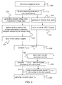
- FIG. 3 three main flows are depicted: 1) the calibration of V REF V BAT ratio and measuring of the internal oscillator frequency (steps 2220-232), 2) the computation of T ON window (step 240) and 3) the generation of the pulse signal T ON . (steps 250-280).
- a triggering signal is generated.
- the triggering signal may drive the generation of the pulse signal T ON (step 280); the signal 6000 on FIG. 6 .
- the triggering signal may further start a first calibration at steps 220, 222 and another calibration at steps 230, 232; the signal 6002 on FIG. 6 .
- the steps of generating the internal clock signal and counting the number CNT of pulses of the internal clock signal (230, 232), and generating the number m (220, 222) may be concomitantly triggered in response to the triggering signal 6002.
- the switching clock period (noted T CLK ) of the DC/DC (or DC-to-DC) converter is divided into k constant time intervals.
- the switching clock of the DC/DC converter is the main clock that provides the pulses controlling the one or more power switches of the DC/DC converter.
- This main switching clock comprises a period noted T CLK .
- the main switching clock may be a pulse width modulated (PWM) signal.
- Dividing T CLK into k constant time intervals does not involve that the main switching clock is modified: dividing T CLK means that a number k of time intervals is determined for each pulse of the main switching cycle. In this case the determination may be a computing operation.
- an internal clock generator may be used as the one 6100 depicted on FIG. 6 .
- the internal clock generator may be an asynchronous clock generator as a ring oscillator.
- the internal clock generator may be a low-consumption clock generator.
- the internal clock generator may be a ring oscillator, e.g. a CMOS ring oscillator.
- the frequency f CLK_INT of the internal clock generator is such that f C ⁇ L ⁇ K _ I ⁇ N ⁇ T > k ⁇ 1 T C ⁇ L ⁇ K .
- the oscillator generates an internal clock signal that allows a division of a switching clock period ( T CLK ) of the DC/DC converter into very small time intervals. In practice, these time intervals may be constant, that is, they have a same duration in time.
- step 230 may be continuously performed.
- step 232 which is activated during a calibration phase, the clock generator frequency is measured in order to measure the internal oscillator clock frequency.
- the oscillator generating the internal clock may be not accurate enough; for instance, when the internal clock generator is a ring oscillator.
- the measurement of the internal clock generator frequency may be performed with an asynchronous counter that counts a number CNT of pulses during one main switching cycle T CLK , which is accurately defined.
- the counter starts the counting at the beginning of the DC/DC main clock cycle T CLK , and stops at the end of this cycle. The number of pulses of the internal clock is thus counted for one main clock cycle T CLK .
- the counted number CNT may be stored into a binary register.
- the asynchronous counter that counts a number CNT of pulses can behave as the binary register. It is to be understood that that the number CNT is in this case a binary number that can vary from one calibration to another.
- an asynchronous counter 6200 that counts a number CNT of pulses is illustrated.
- the calibration counter may also be referred to as calibration counter 6200.
- This asynchronous counter may be comprised a cascade of flip flops ( e.g. D-type flip-flop,), as known in the art. It is to be understood that any circuit able to count the number CNT may be used. Because the counting of the number CNT is performed for a main clock cycle T CLK , a one clock windows filter 6210 may be placed at the entry of the counter 6200. In FIG.
- the internal clock signal oscillating at a approximately 100MHz is counted (or calibrated) during one clock period of the main clock oscillating for instance at 3.2MHz; the main switching period of the DC/DC is thus much longer at least k-times than the period of the internal clock generator, wherein k is an integer.
- V REF is a desired voltage reference at the output of the DC/DC converter and V BAT is the effective voltage at the input of the DC/DC converter.
- V BAT is a working input voltage of the DC-to-DC converter.
- V BAT may be the output voltage of a battery.
- V REF V BAT ratio is performed by block depicted in Fig. 4 , generating a number m that corresponds to the number of discrete equidistant voltage steps ⁇ V of a voltage ramp V CAP before the reference voltage V Ref is reached by the voltage ramp V CAP .
- the calibration may comprise a first step 220 of generating a voltage ramp V CAP of discrete equidistant voltage steps.
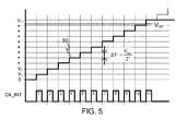
- V CAP is increasing with equidistant voltage steps ⁇ V.
- the passing from a first step (V m ) to a second step ( V m+1 ) may be performed for each pulse of the internal clock so that, for each edge of a pulse, the value of the voltage ramp V CAP increases of ⁇ V.
- a number m that counts the number of discrete equidistant voltage steps V m of the voltage ramp V CAP before the reference voltage V Ref is reached by the voltage ramp V CAP .
- Reaching the reference voltage V Ref means that that the voltage value of V CAP is at least equal to the voltage value of V Ref .
- a voltage ramp 50 is illustrated.
- the number m may be stored into a binary register, the number m being a binary number.
- the results of the calibration are stored in the binary registers, allowing the continuous generation (step 280) of the T ON during the calibration, as well as during the interval when the calibration is in not running.
- the calibration is typically started periodically, e.g. once per second.
- FIG. 4 an example of a calibration unit generating the number m is depicted.
- the number generated by the charge transfer digitizer corresponds accurately to the ratio V REF V BAT ⁇
- the charge transfer digitizer of the ratio V REF V BAT comprises a simple internal logic, described in the following.
- the charge transfer digitizer 4100 on FIG. 4 provides the voltage ramp V CAP , which is compared to reference voltage the reference voltage V REF 4010.
- the voltage ramp V CAP is created by the sequential transfer of electrical charges Q i between a set of capacitors C i , and one main capacitor C 0 .
- the electrical capacities values of C 0 and C i for storing electrical charges should respect the equidistant voltage steps ⁇ V for every m.
- the main capacitor C 0 is further connected on its second side to a third line 4020 providing the voltage ramp V CAP : the voltage of the main capacitor C 0 thus corresponds to the voltage ramp V CAP .
- Each capacitor C i of the set is connected on its second side to a respective switch toggled so that the capacitor C i is connected to a second line 4030 providing V Bat or connected to the third line 4020 providing the voltage ramp V CAP .
- the voltage ramp V CAP is the result of a charge-transfer calibration procedure.
- the discharging of the main capacitor C 0 is performed by a switch 4110 (for instance a transistor acting as switch) short-circuiting the main capacitor C 0 : the switch is closed (for instance the transistor is ON) when no calibration is performed and the switch is open (for instance the transistor is OFF) when the calibration starts.
- the open/close of the switch may be performed as a result of the triggering signal generated at step 200.
- a second step of the charge-transfer calibration procedure the sequential transfer of electrical charges Q i between the set of capacitors C i and one main capacitor C 0 is carried out.
- the voltage of the main capacitor C 0 is the voltage ramp V CAP , and is increased by ⁇ V for every single new pulse of the internal clock.
- V m V BAT 2 N
- each respective switch of a capacitor C i is toggled so that the capacitors C i is connected to the second line 4030 providing V BAT or connected to the third line V CAP .
- all the capacitors of the set may be initially connected to the second line providing the voltage V BAT so that all the capacitors C i are electrically charged V BAT voltage.
- one respective switch of a capacitor C i is toggled for connecting the capacitor in parallel to C 0 . Said otherwise, one respective switch of a capacitor C i is toggled for connecting the capacitor to the third line.
- the switches of the capacitors C i are controlled by a shift register having the internal clock signal as clock input.
- the shift register may be comprised of a cascade of flip flops circuits that share the internal clock, as known in the art.
- the calibration unit may comprise a comparator 4000 on which are connected a first line 4010 providing the reference voltage V REF and a third line 4020 providing the voltage ramp V CAP .
- a first input 4010 is provided on the inverting input (-) of the comparator, and that second input 4020 is provided on the non-inverting input (+) of the comparator.
- the comparator determines that the reference voltage V Ref is reached by the voltage ramp V CAP upon comparison of the voltages on the first and third line, that is, on the first and second inputs.
- the comparator 4000 When the voltage ramp V CAP reaches the reference voltage V REF , the comparator 4000 generates an event and stops the calibration.
- the calibration unit may comprise a counter 4300 for counting the number m.
- the counter that counts the number m starts the counting at the beginning of the calibration procedure and stops at the end of this procedure, that is, once the comparator 4000 stops the calibration. Said otherwise, the counter is started simultaneously with the shift register that controls the toggling of the switches of the capacitors C i of the set and is stopped when the reference voltage V REF is reached by the voltage ramp V CAP .
- the counter has the internal clock signal as clock input and may be an asynchronous or synchronous counter.
- an asynchronous counter 4300 that counts the number m of discrete equidistant voltage steps V m of the voltage ramp V CAP is illustrated.
- This asynchronous counter may be comprised a cascade of flip flops ( e.g. D-type flip-flop,) sharing the same internal clock as the shift register. It is to be understood that any circuit able to count the number m may be used.
- the counter for generating the number m acts also as a binary register for storing the generated number m after the calibration. It is to be understood that the generated number m is in this case a binary number.
- the calibration unit may further comprise a circuit 4400 for generating an output flag V REF_reached when the voltage ramp V CAP is determined as reaching the reference voltage V REF .
- the circuit 4400 may be a Q flip-flop memory cell, as depicted on FIG. 4 . When the output flag V REF_reached is generated, the asynchronous counter 4300 and shift register 4200 are stopped.
- the V REF V BAT value is obtained from the equation (5)
- T ON_WIN is the duration of the pulse signal T ON .
- the accuracy of the generated T ON is given by the division interval k, because the calibration procedure described previously can be done with very high accuracy.
- T ON_WIN is performed by a dedicated computing unit, as the one 6300 illustrated on FIG. 6 .
- the computation of T ON_WIN is performed on binaries values once after the calibration. Indeed, both the numbers m and CNT are stored into a respective binary registers (4300, 6200), and they are therefore binary numbers. It is to be understood that the integration of the invention with digital sub-micro-meter technologies is make easier compared with large-scale analog CMOS technologies.
- a pulse signal T ON driving power switches of a pulse-skipping modulated DC-to-DC converter is generated.
- the pulse signal (T ON ) generation is driven from the computed number T ON_WIN .
- the pulse signal (T ON ) is generated from the computed number T ON_WIN .
- a main counter starts counting and provides a number that is the result of the counting. This main counter is incremented by the generated internal clock signal, e.g. the 100MHz signal generated by block 6100 on FIG. 6 .
- the main counter is reset.
- the conduction cycle T CLK of the DC/DC converter is the time elapsed between two consecutive edges of the pulse when the converter is operating in normal conditions ( i.e. the converter is not running in the pulse-skipping mode).
- the main counter 6500 comprises an edge detector for detecting each edge of the pulse T CLK of the DC/DC converter.
- the edge detector is connected to the reset entry of the counter so that the counter is reset for each detected edge, which signifies the beginning of pulse T CLK .
- the counter is clocked by the internal clock 6100.
- the output of the main counter (that is, the number provided by the main counter) is compared the computed number T ON_WIN .
- the comparison consists in checking the equality between both numbers.
- an equality comparator 6600 having as inputs the computed number T ON_WIN and the number provided by the main counter 6500.
- the equality comparator triggers the stop of the first conduction cycle (upper MOS Q 1 in Fig. 2 ) and can stop the ring oscillator 6100 in order to save the power consumption (step 270).
- the equality comparator triggers the stop of the oscillator generating the internal clock signal (step 270) when the number T ON_WIN and the number provided by the main counter are equal. This advantageously decreases the energy consumption, e.g. the power of the battery connected as input of the DC/DC converter is saved.
- the pulse signal T ON driving power switches of the pulse-skipping modulated DC/DC converter is generated.
- the steps 270 and 280 are simultaneously triggered. Said otherwise, when the computed number T ON_WIN and the number provided by the main counter are equal, the comparator 6600 may reset an output latch 6700 and the generation of the signal T ON is stopped, as illustrated on FIG. 6 .
- the T ON generator system may be implemented on an integrated circuit, e.g. using transistors such as, but not limited to, CMOS transistors.
- the T ON generator is typically an electrical circuit.
- T ON generator system may be implemented with various electronic components suitable to perform the functions.
- the electronic components may be thus packaged discretely, as arrays or networks of like components, or integrated inside of packages such as semiconductor integrated circuits or thick film devices.
- the different values and numbers may be binary values and numbers on which binary mathematical operations can be performed.
- the numbers k, m, CNT may be binary numbers.
- the computed number T ON_WIN may be a binary number.
- the circuit driving the generation of the signal T ON of the present invention can be integrated on switched-mode DC/DC converter comprising power switches and adapted to be modulated by a pulse-skipping modulation.
- the circuit thus manages power switches.
- FIG. 7 it is a time-plot of the generation of the T ON interval.
- the process starts (step 200) at time to with the first request of the calibration: a signal calibrate 6002 goes to High. As a result of this signal, a ring oscillator starts generating the internal clock signal, which is counted (calibrated) during one clock cycle CLK_EXT_3.2MHz.
- a switching clock period T CLK of the DC/DC converter is divided small intervals.
- each conduction cycle T CLK of the DC/DC converter is divided into k time intervals - for instance 32.
- the number of pulses of the internal clock (CLK_INT_100MHZ) shown for one period TCLK is limited.
- the calibration of the ratio V REF V BAT is triggered (steps 220-224) in the same time to as for the starting of internal clock (step 230).
- the calibration unit generates a voltage ramp V CAP , until this ramp reach V REF .
- the number m of steps of the voltage ramp V CAP is now determined, as well as the number CNT of pulses of the internal clock for one main conduction cycle T CLK .
- the computation unit computes the number T ON _window (step 240).
- the pulse signal T ON is generated (step 280) at t 4 and every next beginning of the conduction cycle T CLK .
- the computed reference value T ON_WIN remains constant.
- the output of the generator for generating the pulse signal T ON is set to High.
- the main counter starts to be incremented from zero by the internal ring oscillator of around 100MHz.
- the comparator resets the output latch and sets the generator output to zero.
- the ring oscillator is stopped in order to save power (step 270), e.g. the power of the input battery and the upper MOS in Fig.2 open, whereas its bottom counterpart Q1 closes.
- the generated pulse signal T ON has a duration which is, in this example, shorter than the one half of the signal of the switching clock period T CLK , but it can be also longer.
- V REF V BAT ratio should be run at least once at the beginning of the operation. However, a periodical calibration of V REF V BAT ratio with simultaneous calibration of the ring oscillator frequency (which varies with V BAT and Temperature) is recommended. Indeed, the numbers m and CNT generated may vary with V BAT ( e.g. battery discharging) and the temperature which can be caused by changing of the converter operating conditions. In practice, as shown on FIG. 7 , the calibration signal goes to Low (autoreset) once a time duration of the calibration and computation has elapsed.
Landscapes
- Engineering & Computer Science (AREA)
- Power Engineering (AREA)
- Dc-Dc Converters (AREA)
Abstract
- dividing (210) a switching clock period (TCLK) of the DC-to-DC converter into k constant time intervals;
- generating (230) an internal clock signal having a frequency at least k-time higher than a frequency 1/TCLK of the switching clock;
- counting (232) a number CNT of pulses of the internal clock signal during one clock period of the switching clock period;
- generating an number m (220, 222) that counts a number of discrete equidistant voltage steps ΔV of a voltage ramp VCAP before a reference voltage VRef is reached by the voltage ramp VCAP , each voltage step ΔV being defined by the relation

Description
- The invention relates to the field of step-down switched direct current- direct current (DC/DC) converters, especially switched DC/DC converters with an improved behavior in term of power consumption when operating in light load mode.
- Switching DC/DC converters convert one DC voltage level on the input to another DC voltage level on output. The conversion is performed by storing input energy temporarily and then releasing that energy to the output at a different voltage. During a first phase, the switching DC/DC converter electrically couples a source of the input voltage to a terminal of a reactive element (e.g. an inductor): the reactive element stores magnetic energy from an input current from the input voltage source. In this first phase, the output load receives energy from the input voltage source. In a second phase, the reactive element is disconnected from the input voltage source, and the output load receives the magnetic energy that has been stored in the reactive element during the first phase.
- Acting on the ratio (referred to as duty cycle) between the first phase and second phase durations, it is possible to regulate the transfer of energy from the voltage source to the output load in a controlled way, and thus bring the voltage provided to the output load to the requested value. To this aim, the switching DC/DC converter incorporates a switching regulator for acting on the duty cycle. Most of switching regulators are power switches such as FETs (Field Effect Transistor) that are able to switch efficiently at high frequency. Thus, the average value of voltage fed to a load at the output is controlled by turning the switch between supply and load on and off at a fast pace. In practice, the switch is controlled by a driving signal or pulse, for example by means of square signal. By varying the duty cycle of such pulse in such a way to increase/decrease the duration of the main (first) phase with respect to the second phase, it is possible to increase/decrease the value of the output voltage obtainable by means of the conversion. Since the current request from the output load typically varies during operation, for keeping the output voltage value as stable as possible, the switching DC-DC converters are typically provided with a feedback control circuit, adapted to sense any difference of the output voltage from a desired voltage reference (VREF).
- A pulse skipping mode of a DC/DC (or DC-to-DC) converter is the mode, where the circuit is turned on with lower switching frequency compared to the normal PWM operation of the DC/DC converter: less pulses are generated and the power consumption is therefore considerably reduced. In the pulse skipping mode, the pulses are generated in order to transfer a defined amount of energy into output capacitor, which, in remaining time (that is, when the converter is "skipping") is holding the output voltage. Depending on the application, the pulse skipping mode can presents approximately up to 90% time of operations of the converter. To this aim, a TON generator may be used for dividing the main clock switching period TCLK (which is accurately defined and is in order of MHz) in the times, which ensures, that at the end of the TCLK switching period, the inductor current is very close (say equal) to zero. The time of first phase of conduction is labeled TON and the time of the second phase is labeled TOFF time. The main clock switching period TCLK is accurately fixed and divided such that TON + TOFF = TCLK.
- In practice, this time division is based on an analog calibration scheme using a programmable voltage ramp generator. The ramp generator is based on the continuous-time integrator, whereas the programmability is done by the programmable current source.
- The main drawback of this solution is that it requires continuous running calibration, which implies many active circuits turned-on, thus, having high current consumption. Therefore, the main factor of merit of the switched DC/DC converter, which is power efficiency, is decreased. In addition, in the case of the DC/DC converter having a battery voltage VBAT as input power source, this drawback decreases the battery-life.
- Therefore, existing solutions for accurate generation of the TON time are based on an analog solution having non-negligible power consumption. In addition these solutions do not take care of silicon surface usage, considering this in view of the recent sub-micrometer digital technologies: indeed, DC/DC converters are now available as integrated circuits needing minimal additional components. They are also available as a complete hybrid circuit component, ready for use within an electronic assembly.
- Within this context, there is still a need for a digital TON generator improving power efficiency and integration on silicon surface.
- An object of embodiments of the present invention is to alleviate at least partly the above mentioned drawbacks. More particularly, embodiments of the invention aim at improving the power efficiency and reducing the fabrication cost of the fundamental block of the DC/DC converter operating in the pulse-skipping mode.
- This is achieved with a method for generating a pulse signal (TON) driving power switches of a pulse-skipping modulated DC-to-DC converter. The method comprises dividing a switching clock period (TCLK) of the DC-to-DC converter into k constant time intervals. The method further comprises generating an internal clock signal having a frequency at least k-time higher than a
frequency 1/TCLK of the switching clock. The method also comprises counting a number CNT of pulses of the internal clock signal during one clock period of the switching clock period. The method additionally comprises generating an number m that counts a number of discrete equidistant voltage steps Vm of a voltage ramp VCAP before a reference voltage VREF is reached by the voltage ramp VCAP, each voltage step Vm being defined by the relation

- That the duration of the pulse signal TON is based on the division of TCLK into k constant time intervals of switching clock period of the DC/DC converter and on a number accurately corresponding to the ratio of VREF/VBAT, allow an accurate driving of the switches of the DC/DC converter.
- Embodiments of the invention offer many advantages, including the following:
- the integration on silicon surface is improved because it relies on generation of results relying mainly on digital operations;
- the power consumption is decreased because the invention does not require the use of analog components that have high power consumption;
- the power consumption is decreased because the results of the calibration may be reused for several cycles of the pulse signal TON generation;
- the accuracy of the timing is improved because the pulse signal TON is calibrated according to the state of the power source, reference voltage, temperature and process variations.
- This is also achieved with a circuit for generating a pulse signal (TON) driving power switches in a pulse-skipping modulated DC-to-DC converter. The circuit comprises an oscillator generating an internal clock signal having a frequency at least k-time higher than a
frequency 1/TCLK of the DC-to-DC converter, the switching clock having a period TCLK. The circuit further comprises a calibration unit generating a number m that counts a number of discrete equidistant voltage steps Vm of a voltage ramp VCAP before a reference voltage VREF is reached by the voltage ramp VCAP, each voltage step Vm being defined by the relation
- This is also achieved with the circuit according to the invention implemented on an integrated circuit.
- This is also achieved with a switched-mode DC-to-DC converter with power switches and adapted to be modulated by a pulse-skipping modulation managed by the circuit according to the invention.
- Embodiments of the invention will now be described, by way of non-limiting example, and in reference to the accompanying drawings, where:
-
FIG. 1 an example of a single pulse generation in a pulse-skipping mode of a DC/DC converter; -
FIG. 2 shows an example of a typical DC/DC converter power stage and output filter LC; -
FIG. 3 shows a flowchart of an example of the method; -
FIG. 4 shows a block schematic of an example of a calibration system of
-
FIG. 5 shows an example of discrete voltage ramp generated by a charge transfer mechanism provided by schematic fromFig. 4 ; -
FIG. 6 shows a block schematic diagram of an example of a TON generator system according to the invention; and -
FIG. 7 shows a time-plot of the most important waveforms of the TON generator. - Referring to
FIG. 1 , it is shown the generation of one pulse in the pulse skipping mode of DC/DC (DC-to-DC) converter, where the output voltage of the DC/DC converter connected to the output filter is noted VLX, and the inductor current of the output filter of the DC/DC converter is noted IL. InFIG. 1 , it is considered the case of a typical synchronous DC/DC converter wherein the inductor current always flows through either a first switch Q1 (also referred to as upper MOS) or a second switch Q2 (also referred to as lower MOS), e.g. Q1 and Q2 may be MOSFETs. An example of a typical synchronous DC/DC converter is illustrated onFIG. 2 . During the on-time, Q1 is ON and Q2 is OFF and inductor current increases. During the off-time, Q1 is OFF and Q2 is ON and inductor current decreases. At the on/off transition times, the inductor current has to quickly switch from one MOS to the other one. - In
FIG. 1 , the output voltage VLX starts at the voltage reference VREF, if the previous switching cycle was skipped. When the upper MOS is active (conducting phase) - this phase being also referred to as TON -, the inductor current starts to rise from zero with a positive slope of:
and the VLX voltage is clamped to the positive voltage level of the power source VBAT, e.g. a battery. In the second phase referred to as TOFF, the lower MOS is turned on and the inductor current decreases with negative slope of:
and the VLX voltage is clamped to the negative voltage level of the input power supply. In these equations (1) and (2), VREF stands for the desired output voltage (reference voltage) and L stands for the inductor value. The slopes values are in A/s (ampere per second). - The main purpose of the TON generator is to generate such TON and TOFF intervals so that the inductor current at the end of the conduction cycle TCLK is very close to zero. Indeed, any deviation (i.e. current at the end of the TCLK) either higher or lower than zero implies a high drop of the power efficiency - which implies the decrease of the main factor of merit of the DC/DC converter. This is particularly important for the case where inductance current is inverted.
FIG. 1 shows power losses due to the early or late switch commutation. This is represented by the dashed areas representing looses caused by an inaccurate TON/TOFF generation. - In order to determine the ideal TON and TOFF intervals, the equations (1) and (2) are equalized (3)

what gives:
- It result from the equation (4) that the TON generator aims at dividing the main switching cycle in the pulse-skipping mode in a ratio of the reference voltage VREF to the power supply input voltage VBAT with very high accuracy.
- With reference to the flowchart of
FIG. 3 , it is proposed a method for generating a pulse signal driving power switches of a pulse-skipping modulated DC-to-DC converter. Such a method provides the generation of a pulse signal TON that allows improving power efficiency and integration on silicon surface of the DC/DC converter. In particular, the method of the invention rely on dividing the DC/DC converter switching clock period T CLK into constant intervals, and by mathematical operation provide an appropriate division of the TCLK into TON and TOFF such as:
- By respecting equation(5), the required condition of zero inductor current at the end of conduction cycle is accurately reached, which generator improving power efficiency.
- In
FIG. 3 , three main flows are depicted: 1) the calibration of
- At
step 200, a triggering signal is generated. The triggering signal may drive the generation of the pulse signal TON (step 280); thesignal 6000 onFIG. 6 . The triggering signal may further start a first calibration atsteps steps signal 6002 onFIG. 6 . In practice, the steps of generating the internal clock signal and counting the number CNT of pulses of the internal clock signal (230, 232), and generating the number m (220, 222) may be concomitantly triggered in response to the triggeringsignal 6002. - Next, at
step 210, the switching clock period (noted TCLK) of the DC/DC (or DC-to-DC) converter is divided into k constant time intervals. The switching clock of the DC/DC converter is the main clock that provides the pulses controlling the one or more power switches of the DC/DC converter. This main switching clock comprises a period noted TCLK. In practice, the main switching clock may be a pulse width modulated (PWM) signal. - Dividing TCLK into k constant time intervals does not involve that the main switching clock is modified: dividing TCLK means that a number k of time intervals is determined for each pulse of the main switching cycle. In this case the determination may be a computing operation.
- The number k may be defined by the relation k = 2N, wherein N is a natural number (0 is excluded). For instance, k=32 for N=5.
- Then, at
step 230, an internal clock signal is generated. To this aim, an internal clock generator may be used as the one 6100 depicted onFIG. 6 . In practice, the internal clock generator may be an asynchronous clock generator as a ring oscillator. Preferably, the internal clock generator may be a low-consumption clock generator. The internal clock generator may be a ring oscillator, e.g. a CMOS ring oscillator. The frequency of the clock generator is at least k-time higher than the frequency

- It is to be understood that the
step 230 may be continuously performed. - Then, at
step 232, which is activated during a calibration phase, the clock generator frequency is measured in order to measure the internal oscillator clock frequency. Indeed, the oscillator generating the internal clock may be not accurate enough; for instance, when the internal clock generator is a ring oscillator. - The measurement of the internal clock generator frequency may be performed with an asynchronous counter that counts a number CNT of pulses during one main switching cycle TCLK, which is accurately defined. The counter starts the counting at the beginning of the DC/DC main clock cycle TCLK, and stops at the end of this cycle. The number of pulses of the internal clock is thus counted for one main clock cycle TCLK.
- The counted number CNT may be stored into a binary register. For instance, the asynchronous counter that counts a number CNT of pulses can behave as the binary register. It is to be understood that that the number CNT is in this case a binary number that can vary from one calibration to another.
- Referring to
FIG. 6 , anasynchronous counter 6200 that counts a number CNT of pulses is illustrated. The calibration counter may also be referred to ascalibration counter 6200. This asynchronous counter may be comprised a cascade of flip flops (e.g. D-type flip-flop,), as known in the art. It is to be understood that any circuit able to count the number CNT may be used. Because the counting of the number CNT is performed for a main clock cycle TCLK, a one clock windows filter 6210 may be placed at the entry of thecounter 6200. InFIG. 6 , the internal clock signal oscillating at a approximately 100MHz is counted (or calibrated) during one clock period of the main clock oscillating for instance at 3.2MHz; the main switching period of the DC/DC is thus much longer at least k-times than the period of the internal clock generator, wherein k is an integer. - Referring back at
FIG. 3 , atsteps 220 to 224, another calibration is performed allowing to determine the ratio

step 210, the main switching clock period of the DC/DC converter has been divided into k constant time intervals, wherein k is defined by the relation k = 2N with N that is an integer number. - The calibration of

Fig. 4 , generating a number m that corresponds to the number of discrete equidistant voltage steps ΔV of a voltage ramp VCAP before the reference voltage VRef is reached by the voltage ramp VCAP. - To this aim, the calibration may comprise a
first step 220 of generating a voltage ramp VCAP of discrete equidistant voltage steps. VCAP is increasing with equidistant voltage steps ΔV. The passing from a first step (Vm) to a second step ( Vm+1) may be performed for each pulse of the internal clock so that, for each edge of a pulse, the value of the voltage ramp VCAP increases of ΔV. In practice, each voltage step ΔV is defined by the relation
- Then, it is determined at step 222 a number m that counts the number of discrete equidistant voltage steps Vm of the voltage ramp VCAP before the reference voltage VRef is reached by the voltage ramp VCAP. Reaching the reference voltage VRef means that that the voltage value of VCAP is at least equal to the voltage value of VRef.
- Referring now to
FIG. 5 , avoltage ramp 50 is illustrated. For each pulse of the internal clock, the value of the voltage ramp VCAP increases of
Fig. 5 example until an eleventh pulse of the internal clock is triggered: for m = 11, the value of VCAP is such that VCAP = Vm=11 > VREF, that is voltage ramp has reached the reference voltage what is detected by thecomparator 4000 illustrated onFIG. 4 . The calibration is stops for m = 11. - Referring back to
FIG. 3 , atstep 224, the number m may be stored into a binary register, the number m being a binary number. By this way, it is possible the results of the calibration are stored in the binary registers, allowing the continuous generation (step 280) of the TON during the calibration, as well as during the interval when the calibration is in not running. Furthermore, while the calibration is not running, only small part of the circuit is running, which implies very low power consumption, e.g. in order of 10µA. The calibration is typically started periodically, e.g. once per second. - Referring now to
FIG. 4 , an example of a calibration unit generating the number m is depicted. The sequence of calibration is automatically driven by a charge transfer digitizer of the ratio


- The
charge transfer digitizer 4100 onFIG. 4 provides the voltage ramp VCAP, which is compared to reference voltage thereference voltage V REF 4010. The voltage ramp VCAP is created by the sequential transfer of electrical charges Qi between a set of capacitors Ci, and one main capacitor C0. The number of capacitor may be a simple design choice, forinstance 2N. In practice, the number of capacitor is equal to the number k, but the highest capacitors are not integrated as VREF is always lower than VBAT. For instance, thecharge transfer digitizer 4100 would have one main capacitor C0 and 31 capacitors Ci for k=32. The electrical capacities values of C0 and Ci for storing electrical charges should respect the equidistant voltage steps ΔV for every m. - All the capacitors are connected on grounded side. This amounts to say that all the capacitors are mounted in parallel and grounded on one side. The main capacitor C0 is further connected on its second side to a
third line 4020 providing the voltage ramp VCAP : the voltage of the main capacitor C0 thus corresponds to the voltage ramp VCAP. Each capacitor Ci of the set is connected on its second side to a respective switch toggled so that the capacitor Ci is connected to asecond line 4030 providing VBat or connected to thethird line 4020 providing the voltage ramp VCAP. - The voltage ramp VCAP is the result of a charge-transfer calibration procedure.
- In a first step of the charge-transfer calibration procedure, the main capacitor C0 is discharged, that is, the voltage VCAP = 0. In practice, the discharging of the main capacitor C0 is performed by a switch 4110 (for instance a transistor acting as switch) short-circuiting the main capacitor C0: the switch is closed (for instance the transistor is ON) when no calibration is performed and the switch is open (for instance the transistor is OFF) when the calibration starts. The open/close of the switch may be performed as a result of the triggering signal generated at
step 200. - In a second step of the charge-transfer calibration procedure, the sequential transfer of electrical charges Qi between the set of capacitors Ci and one main capacitor C0 is carried out. The voltage of the main capacitor C0, is the voltage ramp VCAP, and is increased by ΔV for every single new pulse of the internal clock. When considering the grounded main capacitor C0, with initial voltage VC0+= 0, and by applying a charge stored in a capacitor C1 charged to VBAT, the voltage step is of:

- When considering equidistant voltage steps Vm, the equation (6) may be generalized for any mth voltage as:

where k=2N is the clock period division constant. It results from the equation (7) the voltage step size is:
- This constant voltage steps can be obtained for the capacitor selected by following the rule:

where j is the j-th capacitor inFIG. 4 . If this equation is fulfilled, the voltage VCAP is increasing with discrete equidistant steps ΔV, as shown inFIG. 5 . - During the calibration, each respective switch of a capacitor Ci is toggled so that the capacitors Ci is connected to the
second line 4030 providing VBAT or connected to the third line VCAP. In practice, all the capacitors of the set may be initially connected to the second line providing the voltage VBAT so that all the capacitors Ci are electrically charged VBAT voltage. For each pulse of the internal clock, one respective switch of a capacitor Ci is toggled for connecting the capacitor in parallel to C0. Said otherwise, one respective switch of a capacitor Ci is toggled for connecting the capacitor to the third line. - The switches of the capacitors Ci are controlled by a shift register having the internal clock signal as clock input. The shift register may be comprised of a cascade of flip flops circuits that share the internal clock, as known in the art.
- The calibration unit may comprise a
comparator 4000 on which are connected afirst line 4010 providing the reference voltage VREF and athird line 4020 providing the voltage ramp VCAP. This amounts to say that afirst input 4010 is provided on the inverting input (-) of the comparator, and thatsecond input 4020 is provided on the non-inverting input (+) of the comparator. The comparator determines that the reference voltage VRef is reached by the voltage ramp VCAP upon comparison of the voltages on the first and third line, that is, on the first and second inputs. When the voltage ramp VCAP reaches the reference voltage VREF, thecomparator 4000 generates an event and stops the calibration. - The calibration unit may comprise a
counter 4300 for counting the number m. The counter that counts the number m starts the counting at the beginning of the calibration procedure and stops at the end of this procedure, that is, once thecomparator 4000 stops the calibration. Said otherwise, the counter is started simultaneously with the shift register that controls the toggling of the switches of the capacitors Ci of the set and is stopped when the reference voltage VREF is reached by the voltage ramp VCAP. The counter has the internal clock signal as clock input and may be an asynchronous or synchronous counter. - Still referring to
FIG. 4 , anasynchronous counter 4300 that counts the number m of discrete equidistant voltage steps Vm of the voltage ramp VCAP is illustrated. This asynchronous counter may be comprised a cascade of flip flops (e.g. D-type flip-flop,) sharing the same internal clock as the shift register. It is to be understood that any circuit able to count the number m may be used. - In practice, the counter for generating the number m acts also as a binary register for storing the generated number m after the calibration. It is to be understood that the generated number m is in this case a binary number.
- The calibration unit may further comprise a
circuit 4400 for generating an output flag VREF_reached when the voltage ramp VCAP is determined as reaching the reference voltage VREF. Thecircuit 4400 may be a Q flip-flop memory cell, as depicted onFIG. 4 . When the output flag VREF_reached is generated, theasynchronous counter 4300 andshift register 4200 are stopped. - Referring back to
FIG. 3 , atstep 240, a binary number TON_WIN is computed from the calibrated


- The computation of TON_WIN is performed by a dedicated computing unit, as the one 6300 illustrated on
FIG. 6 . In the electrical circuit driving the generation of TON signal ofFIG. 6 , the computation of TON_WIN is performed on binaries values once after the calibration. Indeed, both the numbers m and CNT are stored into a respective binary registers (4300, 6200), and they are therefore binary numbers. It is to be understood that the integration of the invention with digital sub-micro-meter technologies is make easier compared with large-scale analog CMOS technologies. - Referring back to
FIG. 3 , atsteps 250 to 280, a pulse signal TON driving power switches of a pulse-skipping modulated DC-to-DC converter is generated. The pulse signal (TON) generation is driven from the computed number TON_WIN. Said otherwise, the pulse signal (TON) is generated from the computed number TON_WIN .Atstep 250, a main counter starts counting and provides a number that is the result of the counting. This main counter is incremented by the generated internal clock signal, e.g. the 100MHz signal generated byblock 6100 onFIG. 6 . At the beginning of each conduction cycle of the DC/DC converter, the main counter is reset. The conduction cycle TCLK of the DC/DC converter is the time elapsed between two consecutive edges of the pulse when the converter is operating in normal conditions (i.e. the converter is not running in the pulse-skipping mode). - Referring now to
FIG. 6 , themain counter 6500 is illustrated. It comprises an edge detector for detecting each edge of the pulse TCLK of the DC/DC converter. The edge detector is connected to the reset entry of the counter so that the counter is reset for each detected edge, which signifies the beginning of pulse TCLK. The counter is clocked by theinternal clock 6100. - Then, at
step 260, the output of the main counter (that is, the number provided by the main counter) is compared the computed number TON_WIN. The comparison consists in checking the equality between both numbers. - Referring back to
FIG. 6 , it depicted anequality comparator 6600 having as inputs the computed number TON_WIN and the number provided by themain counter 6500. The equality comparator triggers the stop of the first conduction cycle (upper MOS Q1 inFig. 2 ) and can stop thering oscillator 6100 in order to save the power consumption (step 270). In other terms, the equality comparator triggers the stop of the oscillator generating the internal clock signal (step 270) when the number TON_WIN and the number provided by the main counter are equal. This advantageously decreases the energy consumption, e.g. the power of the battery connected as input of the DC/DC converter is saved. - At
step 280, the pulse signal TON driving power switches of the pulse-skipping modulated DC/DC converter is generated. In practice, thesteps comparator 6600 may reset anoutput latch 6700 and the generation of the signal TON is stopped, as illustrated onFIG. 6 . - It is to be understood that the TON generator system according to the invention may be implemented on an integrated circuit, e.g. using transistors such as, but not limited to, CMOS transistors. The TON generator is typically an electrical circuit. It is to be understood that TON generator system may be implemented with various electronic components suitable to perform the functions. The electronic components may be thus packaged discretely, as arrays or networks of like components, or integrated inside of packages such as semiconductor integrated circuits or thick film devices. It is to be understood that the different values and numbers may be binary values and numbers on which binary mathematical operations can be performed. For instance, the numbers k, m, CNT may be binary numbers. As another example, the computed number TON_WIN may be a binary number. Interestingly, using binary number and values allow to make possible a digital implementation of the pulse signal TON generator, e.g. on an integrated circuit. Furthermore, due to the very good inherent matching of the capacitors in modem CMOS process, the final accuracy of the calibration is very high.
- In practice, the circuit driving the generation of the signal TON of the present invention can be integrated on switched-mode DC/DC converter comprising power switches and adapted to be modulated by a pulse-skipping modulation. The circuit thus manages power switches.
- Referring now to
FIG. 7 , it is a time-plot of the generation of the TON interval. - The process starts (step 200) at time to with the first request of the calibration: a signal calibrate 6002 goes to High. As a result of this signal, a ring oscillator starts generating the internal clock signal, which is counted (calibrated) during one clock cycle CLK_EXT_3.2MHz. Here, a switching clock period TCLK of the DC/DC converter is divided small intervals. Moreover, each conduction cycle TCLK of the DC/DC converter is divided into k time intervals - for instance 32. For the sake of clarity of the
FIG. 7 , the number of pulses of the internal clock (CLK_INT_100MHZ) shown for one period TCLK is limited. - The calibration of the ratio


- Then, the pulse signal TON is generated (step 280) at t4 and every next beginning of the conduction cycle TCLK. During the generation of the pulse signal TON, the computed reference value TON_WIN remains constant. At the beginning of the main conduction cycle TCLK, at t4, the output of the generator for generating the pulse signal TON is set to High. In the same time, at t4, the main counter starts to be incremented from zero by the internal ring oscillator of around 100MHz. When the main counter (step 250) reaches the computed number TON_WIN (step 260), at t5, the comparator resets the output latch and sets the generator output to zero. Simultaneously, the ring oscillator is stopped in order to save power (step 270), e.g. the power of the input battery and the upper MOS in
Fig.2 open, whereas its bottom counterpart Q1 closes. It is noticeable on the figure that the generated pulse signal TON has a duration which is, in this example, shorter than the one half of the signal of the switching clock period TCLK, but it can be also longer. - The calibration of


FIG. 7 , the calibration signal goes to Low (autoreset) once a time duration of the calibration and computation has elapsed.
Claims (14)
- A method for generating a pulse signal (TON) driving power switches of a pulse-skipping modulated DC-to-DC converter, the method comprising:- dividing (210) a switching clock period (TCLK) of the DC-to-DC converter into k constant time intervals;- generating (230) an internal clock signal having a frequency at least k-time higher than a frequency 1/TCLK of the switching clock;- counting (232) a number CNT of pulses of the internal clock signal during one clock period of the switching clock period;- generating an number m (220, 222) that counts a number of discrete equidistant voltage steps ΔV of a voltage ramp VCAP before a reference voltage VREF is reached by the voltage ramp VCAP, each voltage step ΔV being defined by the relation
 - generating the pulse signal (TON) (280) from a computed number TON_WIN such that TON_WIN
- The method of claim 1, further comprising a step of:- storing (224) the generated number m into a binary register.
- The method of any of claims 1 to 2, further comprising the steps of:- starting a main counter (250) that is incremented by the generated internal clock signal and that is reset at the beginning of a conduction cycle of the DC-to-DC converter, the main counter providing a number;- comparing the computed number TON_WIN (260) with the number provided by the main counter; and- stopping (270) the generation of the internal clock signal when the computed number TON_WIN and the number provided by the main counter are equal.
- The method of any of claims 1 to 3, wherein the step (280) of generating the pulse signals (TON) is performed at the beginning of a conduction cycle of the DC-to-DC converter.
- The method of any of claims 1 to 4, wherein the steps of generating the internal clock signal, counting the number CNT of pulses of the internal clock signal, and generating the number m are concomitantly triggered in response to a triggering signal.
- A circuit for generating a pulse signal (TON) driving power switches in a pulse-skipping modulated DC-to-DC converter, the circuit comprising:- an oscillator (6100) generating an internal clock signal having a frequency at least k-time higher than a frequency 1/TCLK of a switching clock of the DC-to-DC converter, the switching clock having a period TCLK;- a calibration unit generating a number m that counts a number of discrete equidistant voltage steps ΔV of a voltage ramp VCAP before a reference voltage VREF is reached by the voltage ramp VCAP, each voltage step ΔV being defined by the relation
 - a counter (6200) for counting a number CNT of pulses of the internal clock signal during one clock period of the switching clock period;- a computing unit (6300) for computing a number TON_WIN such that TON_WIN
 - a generator (6500, 6600, 6700) for generating the pulse signal (TON) from the computed number TON_WIN.
 - The circuit of claim 6, wherein the calibration unit comprises a charge transfer digitizer (4100) of the ratio
 - a first line (4010) providing the reference voltage VREF;- a second line (4030) providing the working input voltage VBAT;- one main capacitor (C0) and a set of capacitors (Ci) mounted in parallel and grounded on one side, the main capacitor (C0) being connected on its second side to a third line (4020) providing the voltage ramp VCAP, and each capacitor (Ci) of the set being connected on its second side to a respective switch toggled so that the capacitor (Ci) is connected to the second or the third line;- a shift register (4200) having the internal clock signal as clock input and controlling the toggling of the switches of the capacitors (Ci) of the set, the switches being controlled so that a supplementary electrical charge of one of the capacitors (Ci) of the set is transferred to the main capacitor (C0) for each pulse of the internal clock signal, a voltage step Vm of the voltage ramp VCAP having a value defined by the relation
- The circuit of any of claims 6 to 7, wherein the calibration unit further comprises a counter (4300) for counting the number m, the counter having the internal clock signal as clock input, the counter being started simultaneously with the shift register that controls the toggling of the switches of the capacitors (Ci) of the set and being stopped when the reference voltage VREF is reached by the voltage ramp VCAP.
- The circuit of any of claim 8, wherein the counter for counting the number m acts as a binary register for storing the generated number m.
- The circuit of any of claims 6 to 9, wherein the calibration unit further comprises a comparator (4000) connected to the first line providing the reference voltage VREF and the third line providing the voltage ramp VCAP, the comparator determining whether VCAP reaches VREF and stopping the shift register when VCAP reaches VREF.
- The circuit of any of claims 6 to 10, wherein the generator of the pulse signal ( TON) comprises an output latch (6700) having as inputs the number TON_WIN and the clock (TCLK) of the DC-to-DC, and providing as output the pulse signal (TON).
- The circuit of any of claims 6 to 11, further comprising an equality comparator (6600) having as inputs the number TON_WIN and a number provided by main counter (6500) that is incremented by the generated internal clock signal and that is reset at the beginning of a conduction cycle of the DC-to-DC converter, the equality comparator triggering the stop of the oscillator generating the internal clock signal when the number TON_WIN and the number provided by the main counter are equal.
- The circuit of any of claims 6 to 12 implemented on an integrated circuit.
- A switched-mode DC-to-DC converter comprising power switches and adapted to be modulated by a pulse-skipping modulation managed by the circuit of any of claims 6 to 13.
Priority Applications (1)
| Application Number | Priority Date | Filing Date | Title |
|---|---|---|---|
| EP12305750.7A EP2680420A1 (en) | 2012-06-26 | 2012-06-26 | Digital on-time signal generator for a low-power pulse-skipping mode of DC-to-DC converter |
Applications Claiming Priority (1)
| Application Number | Priority Date | Filing Date | Title |
|---|---|---|---|
| EP12305750.7A EP2680420A1 (en) | 2012-06-26 | 2012-06-26 | Digital on-time signal generator for a low-power pulse-skipping mode of DC-to-DC converter |
Publications (1)
| Publication Number | Publication Date |
|---|---|
| EP2680420A1 true EP2680420A1 (en) | 2014-01-01 |
Family
ID=46507940
Family Applications (1)
| Application Number | Title | Priority Date | Filing Date |
|---|---|---|---|
| EP12305750.7A Withdrawn EP2680420A1 (en) | 2012-06-26 | 2012-06-26 | Digital on-time signal generator for a low-power pulse-skipping mode of DC-to-DC converter |
Country Status (1)
| Country | Link |
|---|---|
| EP (1) | EP2680420A1 (en) |
Cited By (1)
| Publication number | Priority date | Publication date | Assignee | Title |
|---|---|---|---|---|
| US10044269B2 (en) | 2016-04-30 | 2018-08-07 | Dialog Semiconductor (Uk) Limited | Switching converter with improved recovery time |
-
2012
- 2012-06-26 EP EP12305750.7A patent/EP2680420A1/en not_active Withdrawn
Non-Patent Citations (6)
| Title |
|---|
| AHMED EMIRA ET AL: "DC-DC converter with ON-time control in pulse-skipping modulation", IEEE INTERNATIONAL SYMPOSIUM ON CIRCUITS AND SYSTEMS. ISCAS 2010 - 30 MAY-2 JUNE 2010 - PARIS, FRANCE, IEEE, US, 30 May 2010 (2010-05-30), pages 2746 - 2749, XP031724276, ISBN: 978-1-4244-5308-5 * |
| PATELLA B J ET AL: "High-frequency digital controller IC for DC/DC converters", APEC 2002. 17TH. ANNUAL IEEE APPLIED POWER ELECTRONICS CONFERENCE AND EXPOSITION. DALLAS, TX, MARCH 10 - 14, 2002; [ANNUAL APPLIED POWER ELECTRONICS CONFERENCE], NEW YORK, NY : IEEE, US, vol. CONF. 17, 10 March 2002 (2002-03-10), pages 374 - 380, XP010582947, ISBN: 978-0-7803-7404-1, DOI: 10.1109/APEC.2002.989273 * |
| SYED A ET AL: "Digital pulse width modulator architectures", POWER ELECTRONICS SPECIALISTS CONFERENCE, 2004. PESC 04. 2004 IEEE 35TH ANNUAL, AACHEN, GERMANY 20-25 JUNE 2004, PISCATAWAY, NJ, USA,IEEE, US, vol. 6, 20 June 2004 (2004-06-20), pages 4689 - 4695, XP010739156, ISBN: 978-0-7803-8399-9, DOI: 10.1109/PESC.2004.1354828 * |
| SYED A ET AL: "Digital PWM controller with feed-forward compensation", 2004 IEEE APPLIED POWER ELECTRONICS CONFERENCE AND EXPOSITION, APEC 04, IEEE, ANAHEIM, CA, USA, vol. 1, 22 February 2004 (2004-02-22), pages 60 - 66, XP010703481, ISBN: 978-0-7803-8269-5, DOI: 10.1109/APEC.2004.1295788 * |
| VAHID YOUSEFZADEH ET AL: "Hybrid DPWM with Digital Delay-Locked Loop", COMPUTERS IN POWER ELECTRONICS, 2006. COMPEL '06. IEEE WORKSHOPS ON, IEEE, PI, 1 July 2006 (2006-07-01), pages 142 - 148, XP031044986, ISBN: 978-0-7803-9724-8 * |
| XU ZHANG ET AL: "Digital PWM/PFM controller with input voltage feed-forward for synchronous buck converters", APPLIED POWER ELECTRONICS CONFERENCE AND EXPOSITION, 2008. APEC 2008. TWENTY-THIRD ANNUAL IEEE, IEEE, PISCATAWAY, NJ, USA, 24 February 2008 (2008-02-24), pages 523 - 528, XP031253297, ISBN: 978-1-4244-1873-2 * |
Cited By (1)
| Publication number | Priority date | Publication date | Assignee | Title |
|---|---|---|---|---|
| US10044269B2 (en) | 2016-04-30 | 2018-08-07 | Dialog Semiconductor (Uk) Limited | Switching converter with improved recovery time |
Similar Documents
| Publication | Publication Date | Title |
|---|---|---|
| US9639102B2 (en) | Predictive current sensing | |
| US9627974B1 (en) | Adaptive voltage regulator | |
| US9467137B2 (en) | Input current control method, switch control circuit and power supply including the switch control circuit | |
| US20110316511A1 (en) | Method and apparatus for dc-to-dc conversion | |
| US8872501B2 (en) | Voltage converters with reduced output frequency variations and associated methods | |
| CN102684474B (en) | The mode control circuit of DC-DC converter | |
| Costabeber et al. | Time optimal, parameters-insensitive digital controller for DC-DC buck converters | |
| EP2677647A2 (en) | Synchronous rectifier timer for discontinuous mode DC/DC converter | |
| US20080197821A1 (en) | Dc-dc conversion circuit, dc-dc conversion control circuit, and dc-dc conversion control method | |
| TWI463776B (en) | Bootstrap dc-dc converter | |
| US20140152243A1 (en) | Switching charger, the control circuit and the control method thereof | |
| TW200910746A (en) | Switching DC-DC converter with adaptive-minimum-on-time control and method of adaptively controlling minimum-on-time of a switching DC-DC converter | |
| US9444333B2 (en) | Auto-tuning switching regulator | |
| JP2014207569A (en) | Ramp wave generation circuit | |
| TWI533559B (en) | Circuit in an electronic device and method for powering | |
| EP3312982A1 (en) | Step-up/step-down dc/dc converter | |
| US8941366B2 (en) | DC-DC converter having an output that is a measure of the efficiency of the converter | |
| US20130169327A1 (en) | Charge-to-Digital Timer | |
| CN110830008A (en) | Voltage waveform generating device | |
| US9537390B2 (en) | Control circuit, control method, DC-DC converter and electronic device | |
| CN204666166U (en) | Capacitor charge and discharge control module and power frequency change-over circuit | |
| RU156560U1 (en) | FREQUENCY STAND DEVICE FOR Zeeman LASER GYROSCOPES | |
| US11852663B2 (en) | Voltage monitor using a capacitive digital-to-analog converter | |
| US9294076B2 (en) | Switching power supply device and pulse width modulation circuit used therein | |
| EP2670034A1 (en) | Method and circuit for determining charge pump input current |
Legal Events
| Date | Code | Title | Description |
|---|---|---|---|
| PUAI | Public reference made under article 153(3) epc to a published international application that has entered the european phase |
Free format text: ORIGINAL CODE: 0009012 |
|
| AK | Designated contracting states |
Kind code of ref document: A1 Designated state(s): AL AT BE BG CH CY CZ DE DK EE ES FI FR GB GR HR HU IE IS IT LI LT LU LV MC MK MT NL NO PL PT RO RS SE SI SK SM TR |
|
| AX | Request for extension of the european patent |
Extension state: BA ME |
|
| 17P | Request for examination filed |
Effective date: 20140617 |
|
| RBV | Designated contracting states (corrected) |
Designated state(s): AL AT BE BG CH CY CZ DE DK EE ES FI FR GB GR HR HU IE IS IT LI LT LU LV MC MK MT NL NO PL PT RO RS SE SI SK SM TR |
|
| 17Q | First examination report despatched |
Effective date: 20160901 |
|
| RAP1 | Party data changed (applicant data changed or rights of an application transferred) |
Owner name: OCT CIRCUIT TECHNOLOGIES INTERNATIONAL LIMITED |
|
| STAA | Information on the status of an ep patent application or granted ep patent |
Free format text: STATUS: THE APPLICATION IS DEEMED TO BE WITHDRAWN |
|
| 18D | Application deemed to be withdrawn |
Effective date: 20170112 |