EP2680323A1 - Method for manufacturing a light-emitting diode (LED) - Google Patents
Method for manufacturing a light-emitting diode (LED) Download PDFInfo
- Publication number
- EP2680323A1 EP2680323A1 EP13171545.0A EP13171545A EP2680323A1 EP 2680323 A1 EP2680323 A1 EP 2680323A1 EP 13171545 A EP13171545 A EP 13171545A EP 2680323 A1 EP2680323 A1 EP 2680323A1
- Authority
- EP
- European Patent Office
- Prior art keywords
- sensitive adhesive
- led wafer
- led
- pressure
- adhesive sheet
- Prior art date
- Legal status (The legal status is an assumption and is not a legal conclusion. Google has not performed a legal analysis and makes no representation as to the accuracy of the status listed.)
- Withdrawn
Links
Images




Classifications
-
- H—ELECTRICITY
- H10—SEMICONDUCTOR DEVICES; ELECTRIC SOLID-STATE DEVICES NOT OTHERWISE PROVIDED FOR
- H10H—INORGANIC LIGHT-EMITTING SEMICONDUCTOR DEVICES HAVING POTENTIAL BARRIERS
- H10H20/00—Individual inorganic light-emitting semiconductor devices having potential barriers, e.g. light-emitting diodes [LED]
- H10H20/80—Constructional details
- H10H20/85—Packages
-
- H—ELECTRICITY
- H10—SEMICONDUCTOR DEVICES; ELECTRIC SOLID-STATE DEVICES NOT OTHERWISE PROVIDED FOR
- H10H—INORGANIC LIGHT-EMITTING SEMICONDUCTOR DEVICES HAVING POTENTIAL BARRIERS
- H10H20/00—Individual inorganic light-emitting semiconductor devices having potential barriers, e.g. light-emitting diodes [LED]
- H10H20/01—Manufacture or treatment
-
- H—ELECTRICITY
- H10—SEMICONDUCTOR DEVICES; ELECTRIC SOLID-STATE DEVICES NOT OTHERWISE PROVIDED FOR
- H10H—INORGANIC LIGHT-EMITTING SEMICONDUCTOR DEVICES HAVING POTENTIAL BARRIERS
- H10H20/00—Individual inorganic light-emitting semiconductor devices having potential barriers, e.g. light-emitting diodes [LED]
- H10H20/01—Manufacture or treatment
- H10H20/011—Manufacture or treatment of bodies, e.g. forming semiconductor layers
- H10H20/018—Bonding of wafers
-
- H—ELECTRICITY
- H10—SEMICONDUCTOR DEVICES; ELECTRIC SOLID-STATE DEVICES NOT OTHERWISE PROVIDED FOR
- H10P—GENERIC PROCESSES OR APPARATUS FOR THE MANUFACTURE OR TREATMENT OF DEVICES COVERED BY CLASS H10
- H10P72/00—Handling or holding of wafers, substrates or devices during manufacture or treatment thereof
- H10P72/70—Handling or holding of wafers, substrates or devices during manufacture or treatment thereof for supporting or gripping
- H10P72/74—Handling or holding of wafers, substrates or devices during manufacture or treatment thereof for supporting or gripping using temporarily an auxiliary support
- H10P72/7402—Wafer tapes, e.g. grinding or dicing support tapes
-
- H—ELECTRICITY
- H10—SEMICONDUCTOR DEVICES; ELECTRIC SOLID-STATE DEVICES NOT OTHERWISE PROVIDED FOR
- H10P—GENERIC PROCESSES OR APPARATUS FOR THE MANUFACTURE OR TREATMENT OF DEVICES COVERED BY CLASS H10
- H10P72/00—Handling or holding of wafers, substrates or devices during manufacture or treatment thereof
- H10P72/70—Handling or holding of wafers, substrates or devices during manufacture or treatment thereof for supporting or gripping
- H10P72/74—Handling or holding of wafers, substrates or devices during manufacture or treatment thereof for supporting or gripping using temporarily an auxiliary support
- H10P72/7402—Wafer tapes, e.g. grinding or dicing support tapes
- H10P72/7404—Wafer tapes, e.g. grinding or dicing support tapes the wafer tape being a laminate of three or more layers, e.g. including additional layers beyond a base layer and an uppermost adhesive layer
-
- H—ELECTRICITY
- H10—SEMICONDUCTOR DEVICES; ELECTRIC SOLID-STATE DEVICES NOT OTHERWISE PROVIDED FOR
- H10P—GENERIC PROCESSES OR APPARATUS FOR THE MANUFACTURE OR TREATMENT OF DEVICES COVERED BY CLASS H10
- H10P72/00—Handling or holding of wafers, substrates or devices during manufacture or treatment thereof
- H10P72/70—Handling or holding of wafers, substrates or devices during manufacture or treatment thereof for supporting or gripping
- H10P72/74—Handling or holding of wafers, substrates or devices during manufacture or treatment thereof for supporting or gripping using temporarily an auxiliary support
- H10P72/7416—Handling or holding of wafers, substrates or devices during manufacture or treatment thereof for supporting or gripping using temporarily an auxiliary support used during dicing or grinding
-
- H—ELECTRICITY
- H10—SEMICONDUCTOR DEVICES; ELECTRIC SOLID-STATE DEVICES NOT OTHERWISE PROVIDED FOR
- H10P—GENERIC PROCESSES OR APPARATUS FOR THE MANUFACTURE OR TREATMENT OF DEVICES COVERED BY CLASS H10
- H10P72/00—Handling or holding of wafers, substrates or devices during manufacture or treatment thereof
- H10P72/70—Handling or holding of wafers, substrates or devices during manufacture or treatment thereof for supporting or gripping
- H10P72/74—Handling or holding of wafers, substrates or devices during manufacture or treatment thereof for supporting or gripping using temporarily an auxiliary support
- H10P72/7422—Handling or holding of wafers, substrates or devices during manufacture or treatment thereof for supporting or gripping using temporarily an auxiliary support used to protect an active side of a device or wafer
-
- H—ELECTRICITY
- H10—SEMICONDUCTOR DEVICES; ELECTRIC SOLID-STATE DEVICES NOT OTHERWISE PROVIDED FOR
- H10P—GENERIC PROCESSES OR APPARATUS FOR THE MANUFACTURE OR TREATMENT OF DEVICES COVERED BY CLASS H10
- H10P72/00—Handling or holding of wafers, substrates or devices during manufacture or treatment thereof
- H10P72/70—Handling or holding of wafers, substrates or devices during manufacture or treatment thereof for supporting or gripping
- H10P72/74—Handling or holding of wafers, substrates or devices during manufacture or treatment thereof for supporting or gripping using temporarily an auxiliary support
- H10P72/744—Details of chemical or physical process used for separating the auxiliary support from a device or a wafer
-
- H—ELECTRICITY
- H10—SEMICONDUCTOR DEVICES; ELECTRIC SOLID-STATE DEVICES NOT OTHERWISE PROVIDED FOR
- H10W—GENERIC PACKAGES, INTERCONNECTIONS, CONNECTORS OR OTHER CONSTRUCTIONAL DETAILS OF DEVICES COVERED BY CLASS H10
- H10W72/00—Interconnections or connectors in packages
- H10W72/01—Manufacture or treatment
- H10W72/013—Manufacture or treatment of die-attach connectors
-
- H—ELECTRICITY
- H10—SEMICONDUCTOR DEVICES; ELECTRIC SOLID-STATE DEVICES NOT OTHERWISE PROVIDED FOR
- H10W—GENERIC PACKAGES, INTERCONNECTIONS, CONNECTORS OR OTHER CONSTRUCTIONAL DETAILS OF DEVICES COVERED BY CLASS H10
- H10W72/00—Interconnections or connectors in packages
- H10W72/01—Manufacture or treatment
- H10W72/0198—Manufacture or treatment batch processes
-
- H—ELECTRICITY
- H10—SEMICONDUCTOR DEVICES; ELECTRIC SOLID-STATE DEVICES NOT OTHERWISE PROVIDED FOR
- H10W—GENERIC PACKAGES, INTERCONNECTIONS, CONNECTORS OR OTHER CONSTRUCTIONAL DETAILS OF DEVICES COVERED BY CLASS H10
- H10W72/00—Interconnections or connectors in packages
- H10W72/071—Connecting or disconnecting
- H10W72/073—Connecting or disconnecting of die-attach connectors
Definitions
- the present invention relates to a method of manufacturing an LED.
- a light emitting element is laminated on a substrate to form an LED wafer, and then a surface of the substrate on a side opposite to the light emitting element is ground (back-ground) to thin the substrate (for example, Japanese Patent Application Laid-open Nos. 2005-150675 and 2002-319708 ).
- this grinding is carried out while fixing a surface of the substrate on the light emitting element side to a table via a pressure-sensitive adhesive wax.
- the LED wafer that has undergone grinding is subjected to, for example, steps of heating the wax to release the LED wafer, cleaning the wax adhering on the LED wafer, cutting (dicing) the LED wafer to singulate small element pieces, and forming a reflective layer on the surface of the substrate on the side opposite to the light emitting element.
- the above-mentioned back-grinding step is a step of grinding the LED wafer to be very thin. Therefore, during the grinding, there is a problem in that damage such as cracking easily occurs in the LED wafer. In addition, there are such problems that man-hours are required to apply and clean the wax, and that the environmental load is large because a solvent is used to clean the wax. Moreover, there is a problem in that the LED is negatively affected by cleaning liquid.
- the present invention has been made to address the above-mentioned conventional problem, and has an object to provide a method of manufacturing an LED with a small environmental load, which is simple and capable of manufacturing an LED with high yields by preventing damage to the LED wafer.
- a method of manufacturing an LED according to an embodiment of the present invention includes back-grinding a substrate of an LED wafer including a light emitting element and the substrate, wherein the back-grinding includes fixing the LED wafer to a table via a double-sided pressure-sensitive adhesive sheet, and then grinding the substrate.
- the double-sided pressure-sensitive adhesive sheet includes, on at least one surface thereof, a heat-releasable pressure-sensitive adhesive layer.
- the double-sided pressure-sensitive adhesive sheet includes a base member and a heat-releasable pressure-sensitive adhesive layer formed on one surface of the base member, and the LED wafer is fixed to the table under a state in which the heat-releasable pressure-sensitive adhesive layer is attached to the LED wafer.
- the double-sided pressure-sensitive adhesive sheet includes a base member and a heat-releasable pressure-sensitive adhesive layer formed on one surface of the base member, and the LED wafer is fixed to the table under a state in which the heat-releasable pressure-sensitive adhesive layer is attached to the table.
- the double-sided pressure-sensitive adhesive sheet includes a base member and heat-releasable pressure-sensitive adhesive layers formed on both surfaces of the base member.
- the LED wafer is fixed to the table under a state in which another pressure-sensitive adhesive sheet is further arranged between the double-sided pressure-sensitive adhesive sheet and the LED wafer.
- a method of manufacturing an LED of the present invention includes a back-grinding step of grinding a substrate of an LED wafer including a light emitting element and the substrate.
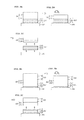
- FIGS. 1A to 1D are schematic views illustrating a back-grinding step in a method of manufacturing an LED according to an embodiment of the present invention.
- FIG. 2 is a schematic sectional view of an LED wafer 100.
- the LED wafer 100 includes a substrate 110 and a light emitting element 120.
- the substrate 110 is made of any appropriate material. Examples of the material for constituting the substrate 110 include sapphire, SiC, GaAs, GaN, and GaP.
- the effect of the present invention that is, preventing damage to the LED wafer 100, is markedly obtained when the employed LED wafer 100 is made of such a hard and brittle material as those materials.
- the LED wafer 100 is fixed to a table 300 via a double-sided pressure-sensitive adhesive sheet 200. At this time, the LED wafer 100 is fixed so that the substrate 110 is directed outward (upward). Subsequently, as illustrated in FIG. 1B , the substrate 110 of the LED wafer 100 is ground. With this grinding, the substrate 110 can be thinned to a desired thickness.
- the thickness of the substrate 110 that has undergone grinding is preferably 10 ⁇ m to 500 ⁇ m, more preferably 50 ⁇ m to 300 ⁇ m, most preferably 80 ⁇ m to 150 ⁇ m.
- the diameter of the employed LED wafer 100 is preferably 2 inches or more, more preferably 3 inches or more, most preferably 4 inches or more.
- the upper limit of the diameter of the LED wafer 100 is not particularly limited, but in practical use, the diameter is about 12 inches, for example.
- the double-sided pressure-sensitive adhesive sheet 200 also has function of protecting the LED wafer 100, and hence the LED wafer 100 may be prevented from being damaged during grinding. Further, the LED wafer 100 can be prevented from being damaged as described above, and hence a large-size (for example, 4 inches or more) LED wafer larger than the conventional one can be handled, and hence the LED can be manufactured with high yields. Subsequently, as illustrated in FIG.
- the LED wafer 100 is released from the table 300.
- the LED wafer 100 may be released from the table 300 while leaving the double-sided pressure-sensitive adhesive sheet 200 on the table 300 ( FIG. 1C ), or the LED wafer with the double-sided pressure-sensitive adhesive sheet may be released from the table 300 ( FIG. 1D ). It is preferred that, as illustrated in FIG. 1D , the LED wafer with the double-sided pressure-sensitive adhesive sheet be released from the table 300. In this manner, the LED wafer 100 may be prevented from being damaged when the LED wafer 100 is released from the table 300.
- the double-sided pressure-sensitive adhesive sheet 200 any appropriate double-sided pressure-sensitive adhesive sheet may be used as long as the effect of the present invention may be obtained.
- the employed double-sided pressure-sensitive adhesive sheet 200 includes a base member 220 and pressure-sensitive adhesive layers 210 formed on both surfaces of the base member 220.
- polyolefins such as polyethylene, polypropylene, polybutene, polybutadiene, and polymethylpentene
- polyvinyl chloride a polyvinyl chloride copolymer, polyethylene terephthalate, polybutylene terephthalate, polyurethane, an ethylene-vinyl acetate copolymer, an ethylene-(meth)acrylic acid copolymer, an ethylene-(meth)acrylate ester copolymer, polystyrene, polycarbonate, polyimide, and a fluorine-based resin.
- the base member there may be given, for example, film, woven fabric, and non-woven fabric.
- the base member may be paper or a metal foil.
- a material for constituting the pressure-sensitive adhesive layer there may be given, for example, a rubber-based resin, an acrylic resin, a silicone-based resin, and a polyimide-based resin.
- the double-sided pressure-sensitive adhesive sheet there is used a double-sided pressure-sensitive adhesive sheet including, on at least one surface thereof, a heat-releasable pressure-sensitive adhesive layer.
- the double-sided pressure-sensitive adhesive sheet including the heat-releasable pressure-sensitive adhesive layer is hereinafter also referred to as "heat-peelable double-sided pressure-sensitive adhesive sheet.”
- the heat-peelable double-sided pressure-sensitive adhesive sheet can be peeled off when the adhesion of the surface of the heat-releasable pressure-sensitive adhesive layer is reduced or lost by heating.
- heat-peelable double-sided pressure-sensitive adhesive sheet 200' and 200" each include the base member 220 and a heat-releasable pressure-sensitive adhesive layer 211.
- the heat-releasable pressure-sensitive adhesive layer 211 includes, for example, an adhesive or pressure-sensitive adhesive, and a foaming agent.
- the heat-peelable double-sided pressure-sensitive adhesive sheet 200' is peeled off when the foaming agent is foamed or expanded by heating.
- Any appropriate adhesive pressure-sensitive adhesive
- the adhesive pressure-sensitive adhesive
- examples thereof include an acrylic adhesive (pressure-sensitive adhesive), a rubber-based adhesive (pressure-sensitive adhesive), and a styrene-conjugated diene block copolymer-based adhesive (pressure-sensitive adhesive).
- Any appropriate foaming agent may be used as the foaming agent.
- the heat-peelable double-sided pressure-sensitive adhesive sheet may include the heat-releasable pressure-sensitive adhesive layer 211 on one surface of the base member 220 as illustrated in FIGS. 3A to 3C and 4A to 4C, or may include the heat-releasable pressure-sensitive adhesive layers 211 on both surfaces of the base member 220 as illustrated in FIGS. 5A to 5C .
Landscapes
- Mechanical Treatment Of Semiconductor (AREA)
- Led Devices (AREA)
Abstract
A method of manufacturing an LED according to an embodiment of the present invention includes back-grinding a substrate of an LED wafer including a light emitting element and the substrate,
wherein the back-grinding includes fixing the LED wafer to a table via a double-sided pressure-sensitive adhesive sheet, and then grinding the substrate.
wherein the back-grinding includes fixing the LED wafer to a table via a double-sided pressure-sensitive adhesive sheet, and then grinding the substrate.
Description
- The present invention relates to a method of manufacturing an LED.
- Hitherto, in manufacture of an LED, a light emitting element is laminated on a substrate to form an LED wafer, and then a surface of the substrate on a side opposite to the light emitting element is ground (back-ground) to thin the substrate (for example, Japanese Patent Application Laid-open Nos.
2005-150675 2002-319708 - The above-mentioned back-grinding step is a step of grinding the LED wafer to be very thin. Therefore, during the grinding, there is a problem in that damage such as cracking easily occurs in the LED wafer. In addition, there are such problems that man-hours are required to apply and clean the wax, and that the environmental load is large because a solvent is used to clean the wax. Moreover, there is a problem in that the LED is negatively affected by cleaning liquid.
- The present invention has been made to address the above-mentioned conventional problem, and has an object to provide a method of manufacturing an LED with a small environmental load, which is simple and capable of manufacturing an LED with high yields by preventing damage to the LED wafer.
- A method of manufacturing an LED according to an embodiment of the present invention includes back-grinding a substrate of an LED wafer including a light emitting element and the substrate,
wherein the back-grinding includes fixing the LED wafer to a table via a double-sided pressure-sensitive adhesive sheet, and then grinding the substrate. - In an embodiment of the present invention, the double-sided pressure-sensitive adhesive sheet includes, on at least one surface thereof, a heat-releasable pressure-sensitive adhesive layer.
- In an embodiment of the present invention, the double-sided pressure-sensitive adhesive sheet includes a base member and a heat-releasable pressure-sensitive adhesive layer formed on one surface of the base member, and the LED wafer is fixed to the table under a state in which the heat-releasable pressure-sensitive adhesive layer is attached to the LED wafer.
- In an embodiment of the present invention, the double-sided pressure-sensitive adhesive sheet includes a base member and a heat-releasable pressure-sensitive adhesive layer formed on one surface of the base member, and the LED wafer is fixed to the table under a state in which the heat-releasable pressure-sensitive adhesive layer is attached to the table.
- In an embodiment of the present invention, the double-sided pressure-sensitive adhesive sheet includes a base member and heat-releasable pressure-sensitive adhesive layers formed on both surfaces of the base member.
- In an embodiment of the present invention, the LED wafer is fixed to the table under a state in which another pressure-sensitive adhesive sheet is further arranged between the double-sided pressure-sensitive adhesive sheet and the LED wafer.
- According to the present invention, in the back-grinding step, after the LED wafer is fixed to the table via the double-sided pressure-sensitive adhesive sheet, the LED wafer is ground. In this manner, the LED wafer may be prevented from being damaged to manufacture the LED with high yields. Further, according to the present invention, wax is unnecessary to fix the LED wafer, and hence application and cleaning of the wax are unnecessary. Therefore, the LED may be simply manufactured. Further, the use of cleaning liquid such as a solvent may be avoided, and hence the LED may be simply manufactured with a small environmental load. Further, an adverse effect to the LED due to the cleaning liquid may be prevented.
- In the accompanying drawings:
-
FIGS. 1A to 1D are schematic views illustrating a back-grinding step in a method of manufacturing an LED according to an embodiment of the present invention; -
FIG. 2 is a schematic sectional view of an LED wafer used in the method of manufacturing an LED according to the embodiment of the present invention; -
FIGS. 3A to 3C are schematic views illustrating a back-grinding step in a method of manufacturing an LED according to another embodiment of the present invention; -
FIGS. 4A to 4C are schematic views illustrating a back-grinding step in a method of manufacturing an LED according to still another embodiment of the present invention; -
FIGS. 5A to 5C are schematic views illustrating a back-grinding step in a method of manufacturing an LED according to further another embodiment of the present invention; -
FIGS. 6A to 6C are schematic views illustrating a back-grinding step in a method of manufacturing an LED according to yet another embodiment of the present invention; -
FIGS. 7A to 7E are schematic views illustrating respective steps after a back-grinding step in a method of manufacturing an LED according to yet another embodiment of the present invention; and -
FIGS. 8A to 8E are schematic views illustrating respective steps after a back-grinding step in a method of manufacturing an LED according to yet another embodiment of the present invention. - A method of manufacturing an LED of the present invention includes a back-grinding step of grinding a substrate of an LED wafer including a light emitting element and the substrate.
-
FIGS. 1A to 1D are schematic views illustrating a back-grinding step in a method of manufacturing an LED according to an embodiment of the present invention. Further,FIG. 2 is a schematic sectional view of anLED wafer 100. TheLED wafer 100 includes asubstrate 110 and alight emitting element 120. Thesubstrate 110 is made of any appropriate material. Examples of the material for constituting thesubstrate 110 include sapphire, SiC, GaAs, GaN, and GaP. The effect of the present invention, that is, preventing damage to theLED wafer 100, is markedly obtained when the employedLED wafer 100 is made of such a hard and brittle material as those materials. Thelight emitting element 120 includes abuffer layer 1, an n-type semiconductor layer 2, alight emitting layer 3, a p-type semiconductor layer 4, atransparent electrode 5, andelectrodes 6 and 7. Thelight emitting layer 3 includes, for example, gallium nitride-based compounds (e.g., GaN, AlGaN, and InGaN), gallium phosphide-based compounds (e.g., GaP and GaAsP), gallium arsenide-based compounds (e.g., GaAs, AlGaAs, and AlGaInP), and zinc oxide (ZnO)-based compounds. Note that, although not illustrated, thelight emitting element 120 may include any other appropriate members. - In the method of manufacturing an LED of the present invention, first, as illustrated in
FIG. 1A , theLED wafer 100 is fixed to a table 300 via a double-sided pressure-sensitiveadhesive sheet 200. At this time, theLED wafer 100 is fixed so that thesubstrate 110 is directed outward (upward). Subsequently, as illustrated inFIG. 1B , thesubstrate 110 of theLED wafer 100 is ground. With this grinding, thesubstrate 110 can be thinned to a desired thickness. The thickness of thesubstrate 110 that has undergone grinding is preferably 10 µm to 500 µm, more preferably 50 µm to 300 µm, most preferably 80 µm to 150 µm. Further, the diameter of the employedLED wafer 100 is preferably 2 inches or more, more preferably 3 inches or more, most preferably 4 inches or more. The upper limit of the diameter of theLED wafer 100 is not particularly limited, but in practical use, the diameter is about 12 inches, for example. In the method of manufacturing an LED of the present invention, the double-sided pressure-sensitive adhesive sheet 200 also has function of protecting theLED wafer 100, and hence theLED wafer 100 may be prevented from being damaged during grinding. Further, theLED wafer 100 can be prevented from being damaged as described above, and hence a large-size (for example, 4 inches or more) LED wafer larger than the conventional one can be handled, and hence the LED can be manufactured with high yields. Subsequently, as illustrated inFIG. 1C or 1D , theLED wafer 100 is released from the table 300. At this time, only theLED wafer 100 may be released from the table 300 while leaving the double-sided pressure-sensitive adhesive sheet 200 on the table 300 (FIG. 1C ), or the LED wafer with the double-sided pressure-sensitive adhesive sheet may be released from the table 300 (FIG. 1D ). It is preferred that, as illustrated inFIG. 1D , the LED wafer with the double-sided pressure-sensitive adhesive sheet be released from the table 300. In this manner, theLED wafer 100 may be prevented from being damaged when theLED wafer 100 is released from the table 300. - As the double-sided pressure-
sensitive adhesive sheet 200, any appropriate double-sided pressure-sensitive adhesive sheet may be used as long as the effect of the present invention may be obtained. In an embodiment, as illustrated inFIGS. 1A to 1D , the employed double-sided pressure-sensitive adhesive sheet 200 includes abase member 220 and pressure-sensitiveadhesive layers 210 formed on both surfaces of thebase member 220. As a material for constituting the base member, there may be given, for example: polyolefins such as polyethylene, polypropylene, polybutene, polybutadiene, and polymethylpentene; and polyvinyl chloride, a polyvinyl chloride copolymer, polyethylene terephthalate, polybutylene terephthalate, polyurethane, an ethylene-vinyl acetate copolymer, an ethylene-(meth)acrylic acid copolymer, an ethylene-(meth)acrylate ester copolymer, polystyrene, polycarbonate, polyimide, and a fluorine-based resin. As a form of the base member, there may be given, for example, film, woven fabric, and non-woven fabric. In addition, the base member may be paper or a metal foil. As a material for constituting the pressure-sensitive adhesive layer, there may be given, for example, a rubber-based resin, an acrylic resin, a silicone-based resin, and a polyimide-based resin. - In other embodiments of the present invention, as the double-sided pressure-sensitive adhesive sheet, there is used a double-sided pressure-sensitive adhesive sheet including, on at least one surface thereof, a heat-releasable pressure-sensitive adhesive layer. In this specification, the double-sided pressure-sensitive adhesive sheet including the heat-releasable pressure-sensitive adhesive layer is hereinafter also referred to as "heat-peelable double-sided pressure-sensitive adhesive sheet." The heat-peelable double-sided pressure-sensitive adhesive sheet can be peeled off when the adhesion of the surface of the heat-releasable pressure-sensitive adhesive layer is reduced or lost by heating. With use of the heat-peelable double-sided pressure-sensitive adhesive sheet, the LED wafer is sufficiently fixed during grinding, and after the grinding, the LED wafer can be easily released. As a result, the LED wafer can be prevented from being damaged more markedly. Further, automated steps can be easily designed. As illustrated in
FIGS. 3A to 3C, 4A to 4C, and5A to 5C, heat-peelable double-sided pressure-sensitive adhesive sheets 200' and 200" each include thebase member 220 and a heat-releasable pressure-sensitive adhesive layer 211. The heat-releasable pressure-sensitive adhesive layer 211 includes, for example, an adhesive or pressure-sensitive adhesive, and a foaming agent. The heat-peelable double-sided pressure-sensitive adhesive sheet 200' is peeled off when the foaming agent is foamed or expanded by heating. Any appropriate adhesive (pressure-sensitive adhesive) may be used as the adhesive (pressure-sensitive adhesive), and examples thereof include an acrylic adhesive (pressure-sensitive adhesive), a rubber-based adhesive (pressure-sensitive adhesive), and a styrene-conjugated diene block copolymer-based adhesive (pressure-sensitive adhesive). Any appropriate foaming agent may be used as the foaming agent. Examples of the foaming agent include: inorganic foaming agents such as ammonium carbonate, ammonium hydrogen carbonate, sodium hydrogen carbonate, ammonium nitrite, sodium boron hydride, and an azide; and organic foaming agents such as an alkane chloride fluoride, an azo-based compound, a hydrazine-based compound, a semicarbazide-based compound, a triazole-based compound, and an N-nitroso-based compound. Details of such a heat-peelable double-sided pressure-sensitive adhesive sheet are described in Japanese Patent Application Laid-open Nos.Hei 5-043851 Hei 2-305878 Sho 63-33487 - When the heat-peelable double-sided pressure-sensitive adhesive sheet is used as the double-sided pressure-sensitive adhesive sheet, the heat-peelable double-sided pressure-sensitive adhesive sheet may include the heat-releasable pressure-
sensitive adhesive layer 211 on one surface of thebase member 220 as illustrated inFIGS. 3A to 3C and 4A to 4C, or may include the heat-releasable pressure-sensitiveadhesive layers 211 on both surfaces of thebase member 220 as illustrated inFIGS. 5A to 5C . - In the embodiment illustrated in
FIGS. 3A to 3C , the heat-peelable double-sided pressure-sensitive adhesive sheet 200' includes the heat-releasable pressure-sensitive adhesive layer 211 on one surface of thebase member 220, and theLED wafer 100 is fixed to the table 300 under a state in which the heat-releasable pressure-sensitive adhesive layer 211 is attached to the LED wafer 100 (substantially, to the light emitting element 120). On a surface of the heat-peelable double-sided pressure-sensitive adhesive sheet 200' on a side opposite to the heat-releasable pressure-sensitive adhesive layer 211 (that is, a surface on the table 300 side), the pressure-sensitive adhesive layer 210 may be provided, and the pressure-sensitive adhesive layer 210 side is attached to the table 300 (FIG. 3A ). In the embodiment illustrated inFIGS. 3A to 3C , thesubstrate 110 is ground (FIG. 3B ), and after that, heating is performed so that theLED wafer 100 is released from the heat-peelable double-sided pressure-sensitive adhesive sheet 200' with the surface of the heat-releasable pressure-sensitive adhesive layer as an origin (FIG. 3C ). According to this embodiment, theLED wafer 100 can be prevented from being damaged during grinding. Further, with one operation (heating), theLED wafer 100 can be released. - In the embodiment illustrated in
FIGS. 4A to 4C , the heat-peelable double-sided pressure-sensitive adhesive sheet 200' includes the heat-releasable pressure-sensitive adhesive layer 211 on one surface of thebase member 220, and theLED wafer 100 is fixed to the table 300 under a state in which the heat-releasable pressure-sensitive adhesive layer 211 is attached to the table 300. On a surface of the heat-peelable double-sided pressure-sensitive adhesive sheet 200' on a side opposite to the heat-releasable pressure-sensitive adhesive layer 211 (that is, a surface on theLED wafer 100 side), the pressure-sensitive adhesive layer 210 may be provided, and the pressure-sensitive adhesive layer 210 side is attached to the LED wafer 100 (FIG. 4A ). In the embodiment illustrated inFIGS. 4A to 4C , thesubstrate 110 is ground (FIG. 4B ), and after that, heating is performed so that a laminate including theLED wafer 100 and the heat-peelable double-sided pressure-sensitive adhesive sheet 200' is released from the table 300 with the surface of the heat-releasable pressure-sensitive adhesive layer as an origin (FIG. 4C ). In this embodiment, after that, the heat-peelable double-sided pressure-sensitive adhesive sheet 200' is peeled off from theLED wafer 100. The heat-peelable double-sided pressure-sensitive adhesive sheet 200' may be peeled off immediately after the back-grinding step, or may be peeled off after performing a predetermined post-process (for example, a reflective layer forming step). According to this embodiment, theLED wafer 100 can be prevented from being damaged during grinding and during handling thereafter, and in addition, it is possible to prevent adhesive residue on theLED wafer 100 after the heat-peelable double-sided pressure-sensitive adhesive sheet 200' is peeled off. - In the embodiment illustrated in
FIGS. 5A to 5C , the heat-peelable double-sided pressure-sensitive adhesive sheet 200" includes the heat-releasable pressure-sensitive adhesive layer 211 on both surfaces of the base member 220 (FIG. 5A ). In the embodiment illustrated inFIGS. 5A to 5C , thesubstrate 110 is ground (FIG. 5B ), and after that, heating is performed so that theLED wafer 100 is released and the heat-peelable double-sided pressure-sensitive adhesive sheet 200" is peeled off, respectively, with the surface of the heat-releasable pressure-sensitive adhesive layer as an origin (FIG. 5C ). According to this embodiment, theLED wafer 100 can be prevented from being damaged during grinding. Further, with one operation (heating), theLED wafer 100 can be released. Further, at the same time when theLED wafer 100 is released, the heat-peelable double-sided pressure-sensitive adhesive sheet 200" can be peeled off from the table 300. According to this embodiment, a plurality of LED wafers can be continuously and efficiently processed when the plurality of LED wafers are sequentially subjected to the back-grinding step. - Further, according to yet another embodiment of the present invention, as illustrated in
FIG. 6A , theLED wafer 100 is fixed to the table 300 under a state in which another pressure-sensitive adhesive sheet 400 is further arranged between the heat-peelable double-sided pressure-sensitive adhesive sheet 200' and theLED wafer 100. Specifically, the another pressure-sensitive adhesive sheet 400 may be arranged between the heat-releasable pressure-sensitive adhesive layer 211 of the heat-peelable double-sided pressure-sensitive adhesive sheet 200' and thelight emitting element 120 of theLED wafer 100. In this embodiment, thesubstrate 110 is ground (FIG. 6B ), and after that, heating is performed so that a laminate including theLED wafer 100 and the another pressure-sensitive adhesive sheet 400 is released from the heat-peelable double-sided pressure-sensitive adhesive sheet 200' with the surface of the heat-releasable pressure-sensitive adhesive layer as an origin (FIG. 6C ). In this embodiment, after that, the another pressure-sensitive adhesive sheet 400 is peeled off from theLED wafer 100. The another pressure-sensitive adhesive sheet 400 may be peeled off immediately after the back-grinding step, or may be peeled off after performing a predetermined post-process (for example, the reflective layer forming step). According to this embodiment, theLED wafer 100 can be prevented from being damaged during grinding and during handling thereafter, and in addition, it is possible to prevent adhesive residue on theLED wafer 100. - As the another pressure-
sensitive adhesive sheet 400, any appropriate pressure-sensitive adhesive sheet may be used. The another pressure-sensitive adhesive sheet 400 includes, for example, abase member 420 and a pressure-sensitive adhesive layer 410 formed on one surface of thebase member 420. As the materials for constituting thebase member 420 and the pressure-sensitive adhesive layer 410, materials similar to those of the double-sided pressure-sensitive adhesive sheet 200 described above may be used. - Note that, referring to
FIGS. 6A to 6C , description has been made of the embodiment in which the heat-peelable double-sided pressure-sensitive adhesive sheet 200' including the heat-releasable pressure-sensitive adhesive layer 211 on one surface of thebase member 220 is used. However, it is needless to say that the heat-peelable double-sided pressure-sensitive adhesive sheet 200" including the heat-releasable pressure-sensitiveadhesive layers 211 on both surfaces of thebase member 220 may be used. - As described above, in the method of manufacturing an LED of the present invention, wax is unnecessary, which has been conventionally necessary to fix the LED wafer. Therefore, according to the present invention, application and cleaning of the wax are unnecessary, and the LED can be simply manufactured. Further, the use of cleaning liquid such as a solvent may be avoided, and hence the LED may be simply manufactured with a small environmental load. Further, an adverse effect to the LED due to the cleaning liquid may be prevented.
- The
LED wafer 100 that has undergone the back-grinding step, in which thesubstrate 110 has been ground as described above, is subjected to steps of the post-process including, for example, a step of cutting theLED wafer 100 to singulate small element pieces (dicing step), and a step of forming a reflective layer on the surface of the substrate on the side opposite to the light emitting element (reflective layer forming step). -
FIGS. 7A to 7E are schematic views illustrating respective steps in a method of manufacturing an LED according to yet another embodiment of the present invention. - In this embodiment, as illustrated in
FIGS. 7A and 7B , theLED wafer 100 that has undergone the back-grinding step, is subjected to the reflective layer forming step. Specifically, theLED wafer 100 is placed on the table 300 with thesubstrate 110 side of theLED wafer 100 up (FIG. 7A ). After that, areflective layer 500 is formed on the outer side of the substrate 110 (FIG. 7B ). By forming thereflective layer 500, the amount of light to be extracted from thelight emitting element 120 can be increased. As a material for constituting thereflective layer 500, any appropriate material may be used as long as the light from thelight emitting element 120 may be satisfactorily reflected. Examples of the material for constituting thereflective layer 500 include metals such as aluminum, silver, gold, palladium, platinum, rhodium, and ruthenium. Thereflective layer 500 made of a metal may be formed by, for example, a vapor deposition method (for example, a metal organic chemical vapor deposition method (MOCVD method)). It is preferred that an underlayer made of, for example, SiO2, TiO2, 2rO2, and/or MgF2 be formed on the outer side of thesubstrate 110 of theLED wafer 100, and then thereflective layer 500 made of a metal be formed by a vapor deposition method. - After the
reflective layer 500 is formed, as illustrated inFIGS. 7C to 7E , theLED wafer 100 having thereflective layer 500 formed thereon is subjected to the dicing step. Specifically, theLED wafer 100 is retained on dicing tape 600 (FIG. 7C ). After that, the LED wafer 100 (substantially, the substrate 110) is half-cut in the thickness direction (FIG. 7D ). After that, the dicingtape 600 is expanded so that theLED wafer 100 having thereflective layer 500 formed thereon is split from the cut portion as an origin to obtainLEDs 700 singulated into small element pieces (FIG. 7E ). - Referring to
FIGS. 7D and 7E , description has been made of the embodiment in which theLED wafer 100 is half-cut so as to split theLED wafer 100 from the cut portion as the origin (scribe dicing). As a method of cutting the LED wafer, in addition to the scribe dicing, any appropriate method may be adopted. Examples of other methods include a method of cutting the LED wafer in the entire thickness direction to singulate the small element pieces through expanding, and a method of laser cutting only the center portion of the LED wafer in the thickness direction to split the LED wafer from the cut portion as an origin (stealth dicing). - Referring to
FIGS. 7A to 7E , description has been made of the embodiment in which, prior to the formation of the cut portion for splitting, the reflective layer forming step is performed. The reflective layer forming step may be performed prior to the formation of the cut portion as described above, or may be performed after the cut portion is formed as illustrated inFIGS. 8A to 8E . In an embodiment of the present invention illustrated inFIGS. 8A to 8E , theLED wafer 100 that has undergone the back-grinding step, is retained on the dicing tape 600 (FIG. 8A ), and after that, theLED wafer 100 is half-cut (FIG. 8B ). Subsequently, theLED wafer 100 having the cut portion formed therein as described above is subjected to the reflective layer forming step. That is, theLED wafer 100 is placed on the table 300 with thelight emitting element 120 side down, and thereflective layer 500 is formed on thesubstrate 110 side of the LED wafer 100 (FIG. 8C ). Subsequently, theLED wafer 100 having thereflective layer 500 formed thereon is retained on the dicingtape 600 again with the side on which the cut portion is formed up (FIG. 8D ). Thus, theLED wafer 100 is split from the cut portion as an origin, to thereby obtain theLEDs 700 singulated into small element pieces (FIG. 8E ). - When the LED wafer that has undergone the back-grinding step includes the double-sided pressure-sensitive adhesive sheet (for example,
FIGS. 1D and4C ), in the post-process, the double-sided pressure-sensitive adhesive sheet is peeled off at any appropriate timing. For example, the LED wafer with the double-sided pressure-sensitive adhesive sheet may be retained on dicing tape, and after that, the double-sided pressure-sensitive adhesive sheet may be peeled off. Then, the operations illustrated inFIG. 8A to 8E may be performed.
Claims (6)
- A method of manufacturing an LED, the method comprising back-grinding a substrate of an LED wafer including a light emitting element and the substrate,
wherein the back-grinding comprises fixing the LED wafer to a table via a double-sided pressure-sensitive adhesive sheet, and then grinding the substrate. - A method of manufacturing an LED according to claim 1, wherein the double-sided pressure-sensitive adhesive sheet comprises, on at least one surface thereof, a heat-releasable pressure-sensitive adhesive layer.
- A method of manufacturing an LED according to claim 2,
wherein the double-sided pressure-sensitive adhesive sheet comprises a base member and a heat-releasable pressure-sensitive adhesive layer formed on one surface of the base member, and
wherein the LED wafer is fixed to the table under a state in which the heat-releasable pressure-sensitive adhesive layer is attached to the LED wafer. - A method of manufacturing an LED according to claim 2,
wherein the double-sided pressure-sensitive adhesive sheet comprises a base member and a heat-releasable pressure-sensitive adhesive layer formed on one surface of the base member, and
wherein the LED wafer is fixed to the table under a state in which the heat-releasable pressure-sensitive adhesive layer is attached to the table. - A method of manufacturing an LED according to claim 2, wherein the double-sided pressure-sensitive adhesive sheet comprises a base member and heat-releasable pressure-sensitive adhesive layers formed on both surfaces of the base member.
- A method of manufacturing an LED according to claim 3 or 5, wherein the LED wafer is fixed to the table under a state in which another pressure-sensitive adhesive sheet is further arranged between the double-sided pressure-sensitive adhesive sheet and the LED wafer.
Applications Claiming Priority (1)
| Application Number | Priority Date | Filing Date | Title |
|---|---|---|---|
| JP2012145449A JP2014011242A (en) | 2012-06-28 | 2012-06-28 | Led manufacturing method |
Publications (1)
| Publication Number | Publication Date |
|---|---|
| EP2680323A1 true EP2680323A1 (en) | 2014-01-01 |
Family
ID=48577617
Family Applications (1)
| Application Number | Title | Priority Date | Filing Date |
|---|---|---|---|
| EP13171545.0A Withdrawn EP2680323A1 (en) | 2012-06-28 | 2013-06-11 | Method for manufacturing a light-emitting diode (LED) |
Country Status (6)
| Country | Link |
|---|---|
| US (1) | US20140000793A1 (en) |
| EP (1) | EP2680323A1 (en) |
| JP (1) | JP2014011242A (en) |
| KR (1) | KR20140001784A (en) |
| CN (1) | CN103531674A (en) |
| TW (1) | TW201407833A (en) |
Families Citing this family (7)
| Publication number | Priority date | Publication date | Assignee | Title |
|---|---|---|---|---|
| US9425418B2 (en) * | 2014-09-30 | 2016-08-23 | Lg Display Co., Ltd. | Flexible display device with bend stress reduction member and manufacturing method for the same |
| CN106716611B (en) | 2014-10-17 | 2019-08-20 | 英特尔公司 | Micro Pick and Bond Assembly |
| JP6354694B2 (en) * | 2015-07-28 | 2018-07-11 | 豊田合成株式会社 | Manufacturing method of semiconductor device |
| EP3477685A4 (en) * | 2016-06-22 | 2020-07-01 | Nissan Chemical Corporation | ADHESIVE WITH POLYDIMETHYL SILOXANE |
| CN106098864A (en) * | 2016-06-28 | 2016-11-09 | 山东浪潮华光光电子股份有限公司 | A kind of pasting method in LED gallium arsenide substrate reduction process |
| KR102708773B1 (en) | 2016-12-26 | 2024-09-23 | 엘지디스플레이 주식회사 | Flexible display device |
| CN119419187A (en) * | 2024-11-05 | 2025-02-11 | 成都莱普科技股份有限公司 | Bonding structure, chip and method for preparing bonding structure |
Citations (15)
| Publication number | Priority date | Publication date | Assignee | Title |
|---|---|---|---|---|
| JPS6333487A (en) | 1987-04-17 | 1988-02-13 | Nitto Electric Ind Co Ltd | Expansion type adhesive sheet |
| JPH02305878A (en) | 1989-05-19 | 1990-12-19 | Nitto Denko Corp | Expandable pressure-sensitive adhesive member |
| JPH0543851A (en) | 1991-08-14 | 1993-02-23 | Nitto Denko Corp | Releasable pressure-sensitive adhesive and self-adhesive member produced therefrom |
| JP2002083785A (en) * | 2000-09-07 | 2002-03-22 | Nec Kansai Ltd | Method for manufacturing semiconductor device |
| US6398892B1 (en) * | 1998-08-26 | 2002-06-04 | Lintec Corporation | Method of using pressure sensitive adhesive double coated sheet |
| JP2002319708A (en) | 2001-04-23 | 2002-10-31 | Matsushita Electric Works Ltd | Led chip and led device |
| WO2004006296A2 (en) * | 2002-06-03 | 2004-01-15 | 3M Innovative Properties Company | Laminate body and corresponding methods and apparatus |
| EP1413615A1 (en) * | 2001-08-03 | 2004-04-28 | Sekisui Chemical Co., Ltd. | Pressure sensitive adhesive double coated tape and method for producing ic chip using it |
| EP1464688A1 (en) * | 2003-03-31 | 2004-10-06 | Nitto Denko Corporation | Heat-peelable double-faced pressure-sensitive adhesive sheet, method for adhering processed material onto said sheet, and electronic part |
| US20050032332A1 (en) * | 2003-06-10 | 2005-02-10 | Saburo Miyamoto | Method for separating semiconductor wafer from supporting member, and apparatus using the same |
| JP2005150675A (en) | 2003-11-18 | 2005-06-09 | Itswell Co Ltd | Semiconductor light emitting diode and manufacturing method thereof |
| US20050215030A1 (en) * | 2004-03-24 | 2005-09-29 | Masayuki Yamamoto | Method and device for separating a reinforcing-plate fixed to a reinforced semiconductor wafer |
| EP1883106A2 (en) * | 2006-07-13 | 2008-01-30 | Nitto Denko Corporation | Method for working object to be worked |
| EP1944345A1 (en) * | 2007-01-15 | 2008-07-16 | Nitto Denko Corporation | Thermal-release double-coated pressure-sensitive adhesive tape or sheet |
| US20100267219A1 (en) * | 2009-04-20 | 2010-10-21 | Disco Corporation | Optical device wafer processing method |
-
2012
- 2012-06-28 JP JP2012145449A patent/JP2014011242A/en active Pending
-
2013
- 2013-06-10 US US13/913,807 patent/US20140000793A1/en not_active Abandoned
- 2013-06-11 EP EP13171545.0A patent/EP2680323A1/en not_active Withdrawn
- 2013-06-27 KR KR1020130074530A patent/KR20140001784A/en not_active Withdrawn
- 2013-06-28 CN CN201310268817.2A patent/CN103531674A/en active Pending
- 2013-06-28 TW TW102123376A patent/TW201407833A/en unknown
Patent Citations (15)
| Publication number | Priority date | Publication date | Assignee | Title |
|---|---|---|---|---|
| JPS6333487A (en) | 1987-04-17 | 1988-02-13 | Nitto Electric Ind Co Ltd | Expansion type adhesive sheet |
| JPH02305878A (en) | 1989-05-19 | 1990-12-19 | Nitto Denko Corp | Expandable pressure-sensitive adhesive member |
| JPH0543851A (en) | 1991-08-14 | 1993-02-23 | Nitto Denko Corp | Releasable pressure-sensitive adhesive and self-adhesive member produced therefrom |
| US6398892B1 (en) * | 1998-08-26 | 2002-06-04 | Lintec Corporation | Method of using pressure sensitive adhesive double coated sheet |
| JP2002083785A (en) * | 2000-09-07 | 2002-03-22 | Nec Kansai Ltd | Method for manufacturing semiconductor device |
| JP2002319708A (en) | 2001-04-23 | 2002-10-31 | Matsushita Electric Works Ltd | Led chip and led device |
| EP1413615A1 (en) * | 2001-08-03 | 2004-04-28 | Sekisui Chemical Co., Ltd. | Pressure sensitive adhesive double coated tape and method for producing ic chip using it |
| WO2004006296A2 (en) * | 2002-06-03 | 2004-01-15 | 3M Innovative Properties Company | Laminate body and corresponding methods and apparatus |
| EP1464688A1 (en) * | 2003-03-31 | 2004-10-06 | Nitto Denko Corporation | Heat-peelable double-faced pressure-sensitive adhesive sheet, method for adhering processed material onto said sheet, and electronic part |
| US20050032332A1 (en) * | 2003-06-10 | 2005-02-10 | Saburo Miyamoto | Method for separating semiconductor wafer from supporting member, and apparatus using the same |
| JP2005150675A (en) | 2003-11-18 | 2005-06-09 | Itswell Co Ltd | Semiconductor light emitting diode and manufacturing method thereof |
| US20050215030A1 (en) * | 2004-03-24 | 2005-09-29 | Masayuki Yamamoto | Method and device for separating a reinforcing-plate fixed to a reinforced semiconductor wafer |
| EP1883106A2 (en) * | 2006-07-13 | 2008-01-30 | Nitto Denko Corporation | Method for working object to be worked |
| EP1944345A1 (en) * | 2007-01-15 | 2008-07-16 | Nitto Denko Corporation | Thermal-release double-coated pressure-sensitive adhesive tape or sheet |
| US20100267219A1 (en) * | 2009-04-20 | 2010-10-21 | Disco Corporation | Optical device wafer processing method |
Also Published As
| Publication number | Publication date |
|---|---|
| TW201407833A (en) | 2014-02-16 |
| KR20140001784A (en) | 2014-01-07 |
| CN103531674A (en) | 2014-01-22 |
| JP2014011242A (en) | 2014-01-20 |
| US20140000793A1 (en) | 2014-01-02 |
Similar Documents
| Publication | Publication Date | Title |
|---|---|---|
| EP2680323A1 (en) | Method for manufacturing a light-emitting diode (LED) | |
| US8541287B2 (en) | Laser processing method for wafer | |
| CN102468233B (en) | Manufacturing method of laser cutting semiconductor wafer | |
| US9812606B2 (en) | Solid-state transducer devices with optically-transmissive carrier substrates and related systems, methods, and devices | |
| JP5146817B2 (en) | Manufacturing method of semiconductor light emitting device | |
| EP2953171B1 (en) | Method of manufacturing a semiconductor optical device | |
| US20080305570A1 (en) | Led chip production method | |
| EP2426741B1 (en) | Method of fabricating a semiconductor light emitting device | |
| US20120100695A1 (en) | Manufacturing method of semiconductor device | |
| EP2680322A1 (en) | Method of manufacturing an led | |
| EP2680325A2 (en) | Method of manufacturing a light emitting diode | |
| JP2012235012A (en) | Light-emitting element and manufacturing method thereof | |
| JP2010267813A (en) | Light emitting device and manufacturing method thereof | |
| EP2680324A1 (en) | Method of manufacturing a LED | |
| TW201324843A (en) | Manufacturing method of LED | |
| CN116313887A (en) | Semiconductor manufacturing equipment | |
| JP2014157921A (en) | Semiconductor element and manufacturing method of the same | |
| JP2010140956A (en) | Method of holding semiconductor wafer, dicing method and spacer | |
| JP2008140926A (en) | Method for manufacturing light emitting device | |
| JP2017117959A (en) | Semiconductor wafer processing method, semiconductor chip manufacturing method, and processed semiconductor wafer |
Legal Events
| Date | Code | Title | Description |
|---|---|---|---|
| PUAI | Public reference made under article 153(3) epc to a published international application that has entered the european phase |
Free format text: ORIGINAL CODE: 0009012 |
|
| AK | Designated contracting states |
Kind code of ref document: A1 Designated state(s): AL AT BE BG CH CY CZ DE DK EE ES FI FR GB GR HR HU IE IS IT LI LT LU LV MC MK MT NL NO PL PT RO RS SE SI SK SM TR |
|
| AX | Request for extension of the european patent |
Extension state: BA ME |
|
| STAA | Information on the status of an ep patent application or granted ep patent |
Free format text: STATUS: THE APPLICATION IS DEEMED TO BE WITHDRAWN |
|
| 18D | Application deemed to be withdrawn |
Effective date: 20140702 |