EP2680322A1 - Method of manufacturing an led - Google Patents
Method of manufacturing an led Download PDFInfo
- Publication number
- EP2680322A1 EP2680322A1 EP13171522.9A EP13171522A EP2680322A1 EP 2680322 A1 EP2680322 A1 EP 2680322A1 EP 13171522 A EP13171522 A EP 13171522A EP 2680322 A1 EP2680322 A1 EP 2680322A1
- Authority
- EP
- European Patent Office
- Prior art keywords
- led wafer
- protective sheet
- grinding
- led
- substrate
- Prior art date
- Legal status (The legal status is an assumption and is not a legal conclusion. Google has not performed a legal analysis and makes no representation as to the accuracy of the status listed.)
- Withdrawn
Links
Images



Classifications
-
- H—ELECTRICITY
- H10—SEMICONDUCTOR DEVICES; ELECTRIC SOLID-STATE DEVICES NOT OTHERWISE PROVIDED FOR
- H10H—INORGANIC LIGHT-EMITTING SEMICONDUCTOR DEVICES HAVING POTENTIAL BARRIERS
- H10H20/00—Individual inorganic light-emitting semiconductor devices having potential barriers, e.g. light-emitting diodes [LED]
- H10H20/80—Constructional details
- H10H20/85—Packages
-
- H—ELECTRICITY
- H10—SEMICONDUCTOR DEVICES; ELECTRIC SOLID-STATE DEVICES NOT OTHERWISE PROVIDED FOR
- H10H—INORGANIC LIGHT-EMITTING SEMICONDUCTOR DEVICES HAVING POTENTIAL BARRIERS
- H10H20/00—Individual inorganic light-emitting semiconductor devices having potential barriers, e.g. light-emitting diodes [LED]
- H10H20/80—Constructional details
- H10H20/85—Packages
- H10H20/855—Optical field-shaping means, e.g. lenses
- H10H20/856—Reflecting means
-
- H—ELECTRICITY
- H10—SEMICONDUCTOR DEVICES; ELECTRIC SOLID-STATE DEVICES NOT OTHERWISE PROVIDED FOR
- H10H—INORGANIC LIGHT-EMITTING SEMICONDUCTOR DEVICES HAVING POTENTIAL BARRIERS
- H10H20/00—Individual inorganic light-emitting semiconductor devices having potential barriers, e.g. light-emitting diodes [LED]
- H10H20/01—Manufacture or treatment
-
- H—ELECTRICITY
- H10—SEMICONDUCTOR DEVICES; ELECTRIC SOLID-STATE DEVICES NOT OTHERWISE PROVIDED FOR
- H10H—INORGANIC LIGHT-EMITTING SEMICONDUCTOR DEVICES HAVING POTENTIAL BARRIERS
- H10H20/00—Individual inorganic light-emitting semiconductor devices having potential barriers, e.g. light-emitting diodes [LED]
- H10H20/01—Manufacture or treatment
- H10H20/011—Manufacture or treatment of bodies, e.g. forming semiconductor layers
- H10H20/018—Bonding of wafers
-
- H—ELECTRICITY
- H10—SEMICONDUCTOR DEVICES; ELECTRIC SOLID-STATE DEVICES NOT OTHERWISE PROVIDED FOR
- H10H—INORGANIC LIGHT-EMITTING SEMICONDUCTOR DEVICES HAVING POTENTIAL BARRIERS
- H10H20/00—Individual inorganic light-emitting semiconductor devices having potential barriers, e.g. light-emitting diodes [LED]
- H10H20/80—Constructional details
- H10H20/84—Coatings, e.g. passivation layers or antireflective coatings
-
- H—ELECTRICITY
- H10—SEMICONDUCTOR DEVICES; ELECTRIC SOLID-STATE DEVICES NOT OTHERWISE PROVIDED FOR
- H10P—GENERIC PROCESSES OR APPARATUS FOR THE MANUFACTURE OR TREATMENT OF DEVICES COVERED BY CLASS H10
- H10P72/00—Handling or holding of wafers, substrates or devices during manufacture or treatment thereof
- H10P72/70—Handling or holding of wafers, substrates or devices during manufacture or treatment thereof for supporting or gripping
- H10P72/74—Handling or holding of wafers, substrates or devices during manufacture or treatment thereof for supporting or gripping using temporarily an auxiliary support
- H10P72/7416—Handling or holding of wafers, substrates or devices during manufacture or treatment thereof for supporting or gripping using temporarily an auxiliary support used during dicing or grinding
-
- H—ELECTRICITY
- H10—SEMICONDUCTOR DEVICES; ELECTRIC SOLID-STATE DEVICES NOT OTHERWISE PROVIDED FOR
- H10P—GENERIC PROCESSES OR APPARATUS FOR THE MANUFACTURE OR TREATMENT OF DEVICES COVERED BY CLASS H10
- H10P72/00—Handling or holding of wafers, substrates or devices during manufacture or treatment thereof
- H10P72/70—Handling or holding of wafers, substrates or devices during manufacture or treatment thereof for supporting or gripping
- H10P72/74—Handling or holding of wafers, substrates or devices during manufacture or treatment thereof for supporting or gripping using temporarily an auxiliary support
- H10P72/7416—Handling or holding of wafers, substrates or devices during manufacture or treatment thereof for supporting or gripping using temporarily an auxiliary support used during dicing or grinding
- H10P72/742—Handling or holding of wafers, substrates or devices during manufacture or treatment thereof for supporting or gripping using temporarily an auxiliary support used during dicing or grinding involving stretching of the auxiliary support post dicing
Definitions
- the present invention relates to a method of manufacturing an LED.
- a light emitting element is laminated on a substrate to form an LED wafer, and then a surface of the substrate on a side opposite to the light emitting element is ground (back-ground) to thin the substrate (for example, Japanese Patent Application Laid-open Nos. 2005-150675 and 2002-319708 ).
- this grinding is carried out while fixing a surface of the substrate on the light emitting element side to a table via a pressure-sensitive adhesive wax.
- the LED wafer that has undergone grinding is subjected to, for example, steps of heating the wax to release the LED wafer, cleaning the wax adhering on the LED wafer, cutting (dicing) the LED wafer to singulate small element pieces, and forming a reflective layer on the surface of the substrate on the side opposite to the light emitting element.
- the LED wafer that has undergone the back-grinding step is very thin, and hence there is a problem in that, in those steps of the post-process, damage such as cracking easily occurs.
- the present invention has been made to address the above-mentioned conventional problem, and has an object to provide a method of manufacturing an LED, which is capable of manufacturing an LED with high yields by preventing damage to the LED wafer.
- the attaching a protective sheet includes, prior to the back-grinding, attaching the protective sheet on an outer side of the light emitting element of the LED wafer.
- the grinding the substrate in the back-grinding is carried out by attaching the protective sheet to a table via a pressure-sensitive adhesive wax to fix the LED wafer to the table, and the method further comprises, after the grinding the substrate, taking off the protective sheet to remove, from the LED wafer, the pressure-sensitive adhesive wax adhering on the LED wafer with the protective sheet, which has been released from the table.
- the attaching a protective sheet includes, after the grinding the substrate in the back-grinding, attaching the protective sheet on an outer side of the substrate of the LED wafer.
- the method further includes, after the back-grinding, forming a reflective layer.
- the protective sheet is attached to the LED wafer, and thus the damage to the LED wafer may be prevented to manufacture the LED with high yields.
- a method of manufacturing an LED according to the present invention includes attaching a protective sheet to an LED wafer including a light emitting element and a substrate.
- the protective sheet may be attached to the LED wafer prior to a back-grinding step (first embodiment), or the protective sheet may be attached to the LED wafer after the substrate is ground in the back-grinding step (second embodiment).
- the LED wafer is protected by the protective sheet, and thus during the back-grinding step, steps after the back-grinding step, and handling between the steps, the damage (for example, cracking) to the LED wafer can be prevented.
- FIGS. 1A to 1D are schematic views illustrating respective steps of a method of manufacturing an LED according to an embodiment of the present invention.
- FIG. 2 is a schematic sectional view of an LED wafer 10.
- the LED wafer 10 includes a light emitting element 11 and a substrate 12.
- the light emitting element 11 includes a buffer layer 1, an n-type semiconductor layer 2, a light emitting layer 3, a p-type semiconductor layer 4, a transparent electrode 5, and electrodes 6 and 7.
- the light emitting layer 3 includes, for example, gallium nitride-based compounds (e.g., GaN, AlGaN, and InGaN), gallium phosphide-based compounds (e.g., GaP and GaAsP), gallium arsenide-based compounds (e.g., GaAs, AlGaAs, and AlGaInP), and zinc oxide (ZnO) -based compounds.
- gallium nitride-based compounds e.g., GaN, AlGaN, and InGaN
- gallium phosphide-based compounds e.g., GaP and GaAsP
- gallium arsenide-based compounds e.g., GaAs, AlGaAs, and AlGaInP
- zinc oxide (ZnO) -based compounds e.g., zinc oxide (ZnO) -based compounds.
- the light emitting element 11 may include any other appropriate members.
- the substrate 12 is made of any
- a protective sheet 20 is attached onto an outer side of the light emitting element 11 of the LED wafer 10. After that, the LED wafer with the protective sheet is subjected to the back-grinding step ( FIGS. 1B to 1D ).
- a representative protective sheet includes a base member and a pressure-sensitive adhesive layer.
- a material for constituting the base member there may be given, for example: polyolefins such as polyethylene, polypropylene, polybutene, polybutadiene, and polymethylpentene; and polyvinyl chloride, a polyvinyl chloride copolymer, polyethylene terephthalate, polybutylene terephthalate, polyurethane, an ethylene-vinyl acetate copolymer, an ethylene-(meth)acrylic acid copolymer, an ethylene-(meth)acrylate ester copolymer, polystyrene, polycarbonate, polyimide, and a fluorine-based resin.
- polyolefins such as polyethylene, polypropylene, polybutene, polybutadiene, and polymethylpentene
- polyvinyl chloride a polyvinyl chloride copolymer, polyethylene terephthalate, polybut
- the base member there may be given, for example, film, woven fabric, and non-woven fabric.
- the base member may be paper or a metal foil.
- a material for constituting the pressure-sensitive adhesive layer there may be given, for example, a rubber-based resin, an acrylic resin, a silicone-based resin, and a polyimide-based resin.
- the LED wafer with the protective sheet is fixed on a table 100.
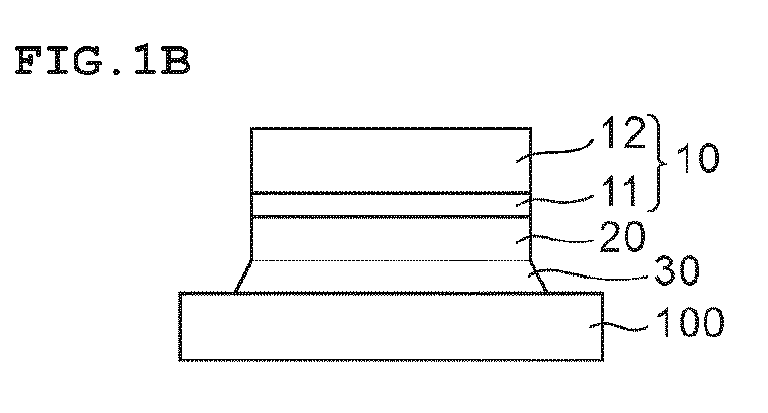
- the LED wafer with the protective sheet is fixed, for example, as illustrated in FIG. 1B , by attaching the protective sheet 20 to the table 100 via a pressure-sensitive adhesive wax 30.
- a pressure-sensitive adhesive wax 30 any appropriate wax may be used as long as the LED wafer 10 may be satisfactorily fixed.
- the pressure-sensitive adhesive wax 30 include paraffin-based wax.
- the LED wafer 10 and the pressure-sensitive adhesive wax 30 are not brought into contact with each other, and hence the LED wafer 10 can be prevented from being stained.
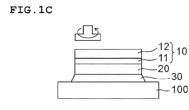
- a surface of the LED wafer 10 on a side opposite to the light emitting element 11 (that is, the substrate 12) is ground.
- the substrate 12 can be thinned to a desired thickness.
- the thickness of the substrate 12 that has undergone grinding is preferably 10 ⁇ m to 500 ⁇ m, more preferably 50 ⁇ m to 300 ⁇ m, most preferably 80 ⁇ m to 150 ⁇ m.
- the diameter of the employed LED wafer 10 is preferably 2 inches or more, more preferably 3 inches or more, most preferably 4 inches or more.
- the upper limit of the diameter of the LED wafer 10 is not particularly limited, but in practical use, the diameter is about 12 inches, for example.
- the LED wafer 10 is protected by the protective sheet 20, and hence the LED wafer 10 may be prevented from being damaged during grinding. Further, the LED wafer 10 can be prevented from being damaged as described above, and hence a large-size (for example, 4 inches or more) LED wafer larger than the conventional one can be handled, and hence the LED can be manufactured with high yields.
- the LED wafer with the protective sheet is released from the table 100.
- heating is performed until the pressure-sensitive adhesive wax 30 exhibits flowability, and thus the LED wafer with the protective sheet is released from the table 100.
- the LED wafer 10 is protected by the protective sheet 20, and hence the LED wafer 10 may be prevented from being damaged when the LED wafer 10 is released from the table 100.
- FIGS. 3A to 3D are schematic views illustrating respective steps of a method of manufacturing an LED according to another embodiment of the present invention.
- the protective sheet is attached to the LED wafer.
- the light emitting element 11 of the LED wafer 10 is attached to the table 100 via the pressure-sensitive adhesive wax 30, to thereby fix the LED wafer 10 onto the table 100.
- the surface of the LED wafer 10 on the side opposite to the light emitting element 11 is ground, to thereby thin the substrate 12.
- FIG. 3B the surface of the LED wafer 10 on the side opposite to the light emitting element 11 (that is, the substrate 12) is ground, to thereby thin the substrate 12.
- the protective sheet 20 is attached to the surface of the LED wafer 10 on the side opposite to the light emitting element 11 (that is, on the outer side of the substrate 12). Subsequently, as illustrated in FIG. 3D , the LED wafer with the protective sheet is released from the table 100. Note that, although not illustrated, in this embodiment, after the LED wafer with the protective sheet is released from the table 100, the pressure-sensitive adhesive wax 30 is cleaned. The pressure-sensitive adhesive wax 30 can be cleaned by immersing the LED wafer with the protective sheet into anorganic solvent which can dissolve the pressure-sensitive adhesive wax.
- the LED wafer 10 is protected by the protective sheet 20, and hence the LED wafer 10 may be prevented from being damaged when the LED wafer 10 is released from the table 100 and handled thereafter.
- the LED wafer 10 that has undergone the back-grinding step, in which the substrate 12 has been ground as described above, is subjected to steps of the post-process including, for example, a step of cutting the LED wafer 10 to singulate small element pieces (dicing step), and a step of forming a reflective layer on the surface of the substrate on the side opposite to the light emitting element (reflective layer forming step).
- steps of the post-process including, for example, a step of cutting the LED wafer 10 to singulate small element pieces (dicing step), and a step of forming a reflective layer on the surface of the substrate on the side opposite to the light emitting element (reflective layer forming step).
- the LED wafer 10 is protected by the protective sheet 20 to prevent damage during the respective steps and handling between the respective steps. Therefore, a large-size (for example, 4 inches or more) LED wafer larger than the conventional one can be handled, and hence the LED can be manufactured with high yields.
- FIGS. 4A to 4F are schematic views illustrating respective steps in a method of manufacturing an LED according to still another embodiment of the present invention.
- FIGS. 4A to 4F illustrate steps subsequent to the back-grinding step for the LED wafer with the protective sheet, which is obtained through the above-mentioned first embodiment (embodiment illustrated in FIGS. 1A to 1D ).
- the LED wafer with the protective sheet which has been subjected to the back-grinding step, is subjected to the reflective layer forming step.
- the LED wafer with the protective sheet is placed on a table 200 with the protective sheet 20 side down ( FIG. 4A ).
- a reflective layer 40 is formed on the LED wafer on a side opposite to the protective sheet (that is, the substrate 12 side) ( FIG. 4B ).
- the reflective layer 40 By forming the reflective layer 40, the amount of light to be extracted from the light emitting element 11 can be increased.
- any appropriate material may be used as long as the light from the light emitting element 11 may be satisfactorily reflected.
- the material for constituting the reflective layer 40 examples include metals such as aluminum, silver, gold, palladium, platinum, rhodium, and ruthenium.
- the reflective layer 40 made of a metal may be formed by, for example, a vapor deposition method (for example, a metal organic chemical vapor deposition method (MOCVD method)). It is preferred that an underlayer formed of, for example, SiO 2 , TiO 2 , ZrO 2 , and/or MgF 2 be formed on the surface of the LED wafer 10 on the side opposite to the light emitting element 11, and then the reflective layer 40 made of a metal be formed by a vapor deposition method.
- a vapor deposition method for example, a metal organic chemical vapor deposition method (MOCVD method)
- MOCVD method metal organic chemical vapor deposition method
- the LED wafer with the protective sheet (LED wafer with the protective sheet formed in the first embodiment) including the protective sheet 20 on the outer side of the light emitting element 11 of the LED wafer 10 is subjected to the reflective layer forming step, and thus the metal may be prevented from being deposited on the light emitting element 11.
- the LED wafer with the protective sheet, which has the reflective layer 40 formed thereon is subjected to the dicing step. Specifically, the LED wafer with the protective sheet, which has the reflective layer 40 formed thereon, is retained on dicing tape 300 with the protective sheet 20 side up ( FIG. 4C ). After that, the protective sheet 20 is peeled off ( FIG. 4D ). Subsequently, the LED wafer 10 (substantially, the substrate 12) is half-cut in the thickness direction from the exposed light emitting element 11 side ( FIG. 4E ) . After that, the dicing tape 300 is expanded so that the LED wafer 10 having the reflective layer 40 formed thereon is split from the cut portion as an origin to obtain LEDs 50 singulated into small element pieces ( FIG. 4F ).
- the LED wafer 10 is half-cut so as to split the LED wafer from the cut portion as the origin (scribe dicing).
- the LED wafer 10 is half-cut from the light emitting element 11 side.
- the dicing tape 300 may be alternatively attached with the substrate 12 (reflective layer 40) side up, and the LED wafer 10 may be half-cut from the substrate 12 side (reflective layer 40 side).
- any appropriate method may be adopted as a method of cutting the LED wafer.
- Examples of other methods include a method of cutting the LED wafer 10 in the entire thickness direction to singulate the small element pieces through expanding, and a method of laser cutting only the center portion of the LED wafer 10 in the thickness direction to split the LED wafer 10 from the cut portion as an origin (stealth dicing).
- the LED wafer with the protective sheet is subjected to the post-process (in FIGS. 4A to 4F , the reflective layer forming step), but the LED wafer may be subjected to the post-process after the protective sheet 20 is peeled off. It is preferred that, as illustrated in FIGS. 4A to 4F , the LED wafer with the protective sheet be subjected to the post-process. This is because, also in the post-process, the thinned LED wafer can be protected, and the damage to the LED wafer can be prevented.
- the reflective layer forming step may be performed prior to the formation of the cut portion as described above, or may be performed after the cut portion is formed as illustrated in FIGS. 5A to 5F and 6A to 6F.
- the LED wafer with the protective sheet which has been subjected to the back-grinding step, is retained on the dicing tape 300 with the protective sheet 20 side up ( FIG. 5A ), and after that, the protective sheet 20 is peeled off ( FIG. 5B ).
- the LED wafer 10 is half-cut from the exposed light emitting element 11 side ( FIG. 5C ) .
- the LED wafer 10 having the cut portion formed therein as described above is subjected to the reflective layer forming step. That is, the LED wafer 10 is placed on the table 200 with the light emitting element 11 side down, and the reflective layer 40 is formed on the substrate 12 side of the LED wafer 10 ( FIG. 5D ).
- the LED wafer 10 having the reflective layer 40 formed thereon is retained on the dicing tape 300 again with the side on which the cut portion is formed (light emitting element 11 side) up ( FIG. 5E ).
- the dicing tape 300 is expanded.
- the LED wafer 10 is split from the cut portion as an origin, to thereby obtain the LEDs 50 singulated into small element pieces ( FIG. 5F ).
- the LED wafer with the protective sheet which has been subjected to the back-grinding step, is retained on the dicing tape 300 with the protective sheet 20 side down ( FIG. 6A ).
- the LED wafer 10 is half-cut from the substrate 12 side ( FIG. 6B ).
- the LED wafer 10 having the cut portion formed therein as described above is subjected to the reflective layer forming step. That is, the LED wafer 10 is placed on the table 200 with the light emitting element 11 side (protective sheet 20 side) down, and the reflective layer 40 is formed on the substrate 12 side of the LED wafer 10 ( FIG. 6C ).
- the LED wafer 10 may be placed on the table 200 under a state in which the dicing tape 300 is still adhering on the outer side of the protective sheet 20, or may be placed on the table 200 after the dicing tape 300 is peeled off (in the illustrated example, the LED wafer 10 is placed after the dicing tape 300 is peeled off). Subsequently, the LED wafer 10 having the reflective layer 40 formed thereon is retained on the dicing tape 300 again with the protective sheet 20 side up ( FIG. 6D ), and then the protective sheet 20 is peeled off ( FIG. 6E ). Then, the dicing tape 300 is expanded. Thus, the LED wafer 10 is split from the cut portion as an origin, to thereby obtain the LEDs 50 singulated into small element pieces ( FIG. 6F ).
- the dicing tape in the dicing step, may be attached with the protective sheet side up, and after that, the protective sheet may be peeled off so as to form the cut portion and split the LED wafer. Further, the LED wafer with the protective sheet, which is obtained through the above-mentioned second embodiment, may be subjected to the dicing step after the protective sheet is peeled off. At this time, the dicing tape may be attached to any one of the light emitting element side and the substrate side of the LED wafer.
- the LED wafer with the protective sheet which is obtained through the above-mentioned second embodiment, may be subjected to the reflective layer forming step after the protective sheet is peeled off.
- the reflective layer forming step may be performed any one of prior to and after the formation of the cut portion, similarly to that performed for the LED wafer obtained through the first embodiment.
Landscapes
- Mechanical Treatment Of Semiconductor (AREA)
- Led Devices (AREA)
Abstract
A method of manufacturing an LED according to an embodiment of the present invention includes:
back-grinding a substrate of an LED wafer including a light emitting element and the substrate; and
attaching a protective sheet to the LED wafer one of prior to the back-grinding and after grinding the substrate in the back-grinding.
back-grinding a substrate of an LED wafer including a light emitting element and the substrate; and
attaching a protective sheet to the LED wafer one of prior to the back-grinding and after grinding the substrate in the back-grinding.
Description
- The present invention relates to a method of manufacturing an LED.
- Hitherto, in manufacture of an LED, a light emitting element is laminated on a substrate to form an LED wafer, and then a surface of the substrate on a side opposite to the light emitting element is ground (back-ground) to thin the substrate (for example, Japanese Patent Application Laid-open Nos.
2005-150675 2002-319708 - The present invention has been made to address the above-mentioned conventional problem, and has an object to provide a method of manufacturing an LED, which is capable of manufacturing an LED with high yields by preventing damage to the LED wafer.
- A method of manufacturing an LED according to an embodiment of the present invention includes:
- back-grinding a substrate of an LED wafer including a light emitting element and the substrate; and
- attaching a protective sheet to the LED wafer one of prior to the back-grinding and after grinding the substrate in the back-grinding.
- In an embodiment of the present invention, the attaching a protective sheet includes, prior to the back-grinding, attaching the protective sheet on an outer side of the light emitting element of the LED wafer.
- In an embodiment of the present invention, the grinding the substrate in the back-grinding is carried out by attaching the protective sheet to a table via a pressure-sensitive adhesive wax to fix the LED wafer to the table, and the method further comprises, after the grinding the substrate, taking off the protective sheet to remove, from the LED wafer, the pressure-sensitive adhesive wax adhering on the LED wafer with the protective sheet, which has been released from the table.
- In an embodiment of the present invention, the attaching a protective sheet includes, after the grinding the substrate in the back-grinding, attaching the protective sheet on an outer side of the substrate of the LED wafer.
- In an embodiment of the present invention, the method further includes, after the back-grinding, forming a reflective layer.
- According to the present invention, the protective sheet is attached to the LED wafer, and thus the damage to the LED wafer may be prevented to manufacture the LED with high yields.
- In the accompanying drawings:
-
FIGS. 1A to 1D are schematic views illustrating respective steps of a method of manufacturing an LED according to an embodiment of the present invention; -
FIG. 2 is a schematic sectional view of an LED wafer used in the method of manufacturing an LED according to the embodiment of the present invention; -
FIGS. 3A to 3D are schematic views illustrating respective steps of a method of manufacturing an LED according to another embodiment of the present invention; -
FIGS. 4A to 4F are schematic views illustrating respective steps after a back-grinding step in a method of manufacturing an LED according to still another embodiment of the present invention; -
FIGS. 5A to 5F are schematic views illustrating respective steps after a back-grinding step in a method of manufacturing an LED according to further another embodiment of the present invention; and -
FIGS. 6A to 6F are schematic views illustrating respective steps after a back-grinding step in a method of manufacturing an LED according to yet another embodiment of the present invention. - A method of manufacturing an LED according to the present invention includes attaching a protective sheet to an LED wafer including a light emitting element and a substrate. In the present invention, the protective sheet may be attached to the LED wafer prior to a back-grinding step (first embodiment), or the protective sheet may be attached to the LED wafer after the substrate is ground in the back-grinding step (second embodiment). In the present invention, the LED wafer is protected by the protective sheet, and thus during the back-grinding step, steps after the back-grinding step, and handling between the steps, the damage (for example, cracking) to the LED wafer can be prevented.
-
FIGS. 1A to 1D are schematic views illustrating respective steps of a method of manufacturing an LED according to an embodiment of the present invention. Further,FIG. 2 is a schematic sectional view of anLED wafer 10. TheLED wafer 10 includes alight emitting element 11 and asubstrate 12. Thelight emitting element 11 includes abuffer layer 1, an n-type semiconductor layer 2, alight emitting layer 3, a p-type semiconductor layer 4, a transparent electrode 5, andelectrodes light emitting layer 3 includes, for example, gallium nitride-based compounds (e.g., GaN, AlGaN, and InGaN), gallium phosphide-based compounds (e.g., GaP and GaAsP), gallium arsenide-based compounds (e.g., GaAs, AlGaAs, and AlGaInP), and zinc oxide (ZnO) -based compounds. Note that, although not illustrated, thelight emitting element 11 may include any other appropriate members. Thesubstrate 12 is made of any appropriate material. Examples of the material for constituting thesubstrate 12 include sapphire, SiC, GaAs, GaN, and GaP. The effects of the present invention are markedly obtained when the employedLED wafer 10 is made of such a hard and brittle material as those materials. - In this embodiment, first, as illustrated in
FIG. 1A , prior to the back-grinding step, aprotective sheet 20 is attached onto an outer side of thelight emitting element 11 of theLED wafer 10. After that, the LED wafer with the protective sheet is subjected to the back-grinding step (FIGS. 1B to 1D ). - As the
protective sheet 20, any appropriate sheet may be used. A representative protective sheet includes a base member and a pressure-sensitive adhesive layer. As a material for constituting the base member, there may be given, for example: polyolefins such as polyethylene, polypropylene, polybutene, polybutadiene, and polymethylpentene; and polyvinyl chloride, a polyvinyl chloride copolymer, polyethylene terephthalate, polybutylene terephthalate, polyurethane, an ethylene-vinyl acetate copolymer, an ethylene-(meth)acrylic acid copolymer, an ethylene-(meth)acrylate ester copolymer, polystyrene, polycarbonate, polyimide, and a fluorine-based resin. As a form of the base member, there may be given, for example, film, woven fabric, and non-woven fabric. In addition, the base member may be paper or a metal foil. As a material for constituting the pressure-sensitive adhesive layer, there may be given, for example, a rubber-based resin, an acrylic resin, a silicone-based resin, and a polyimide-based resin. - In the back-grinding step, the LED wafer with the protective sheet is fixed on a table 100. The LED wafer with the protective sheet is fixed, for example, as illustrated in
FIG. 1B , by attaching theprotective sheet 20 to the table 100 via a pressure-sensitiveadhesive wax 30. As the pressure-sensitiveadhesive wax 30, any appropriate wax may be used as long as theLED wafer 10 may be satisfactorily fixed. Examples of the pressure-sensitiveadhesive wax 30 include paraffin-based wax. In the embodiment illustrated inFIGS. 1A to 1D , the LED wafer 10 and the pressure-sensitiveadhesive wax 30 are not brought into contact with each other, and hence theLED wafer 10 can be prevented from being stained. - After the
LED wafer 10 is fixed as described above, as illustrated inFIG. 1C , a surface of theLED wafer 10 on a side opposite to the light emitting element 11 (that is, the substrate 12) is ground. With this grinding, thesubstrate 12 can be thinned to a desired thickness. The thickness of thesubstrate 12 that has undergone grinding is preferably 10 µm to 500 µm, more preferably 50 µm to 300 µm, most preferably 80 µm to 150 µm. Further, the diameter of the employedLED wafer 10 is preferably 2 inches or more, more preferably 3 inches or more, most preferably 4 inches or more. The upper limit of the diameter of theLED wafer 10 is not particularly limited, but in practical use, the diameter is about 12 inches, for example. In the embodiment illustrated inFIGS. 1A to 1D , theLED wafer 10 is protected by theprotective sheet 20, and hence theLED wafer 10 may be prevented from being damaged during grinding. Further, theLED wafer 10 can be prevented from being damaged as described above, and hence a large-size (for example, 4 inches or more) LED wafer larger than the conventional one can be handled, and hence the LED can be manufactured with high yields. - After the
substrate 12 is ground as described above, as illustrated inFIG. 1D , the LED wafer with the protective sheet is released from the table 100. For example, heating is performed until the pressure-sensitive adhesive wax 30 exhibits flowability, and thus the LED wafer with the protective sheet is released from the table 100. In the embodiment illustrated inFIGS. 1A to 1D , theLED wafer 10 is protected by theprotective sheet 20, and hence theLED wafer 10 may be prevented from being damaged when theLED wafer 10 is released from the table 100. - In the embodiment illustrated in
FIGS. 1A to 1D , it is unnecessary to perform a step of cleaning the pressure-sensitive adhesive wax 30, which has been conventionally necessary after the back-grinding step. This is because, by peeling off theprotective sheet 20 from theLED wafer 10, the pressure-sensitive adhesive wax 30 can also be removed together with theprotective sheet 20. The step of cleaning the pressure-sensitive adhesive wax 30 can be omitted, and hence the use of cleaning liquid such as a solvent can be avoided. Thus, an LED can be simply manufactured with a small environmental load. Further, an adverse effect to the LED due to the cleaning liquid can be prevented. -
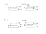
FIGS. 3A to 3D are schematic views illustrating respective steps of a method of manufacturing an LED according to another embodiment of the present invention. In this embodiment, after the substrate is ground in the back-grinding step, the protective sheet is attached to the LED wafer. In this embodiment, as illustrated inFIG. 3A , thelight emitting element 11 of theLED wafer 10 is attached to the table 100 via the pressure-sensitive adhesive wax 30, to thereby fix theLED wafer 10 onto the table 100. Subsequently, as illustrated inFIG. 3B , the surface of theLED wafer 10 on the side opposite to the light emitting element 11 (that is, the substrate 12) is ground, to thereby thin thesubstrate 12. Subsequently, as illustrated inFIG. 3C , theprotective sheet 20 is attached to the surface of theLED wafer 10 on the side opposite to the light emitting element 11 (that is, on the outer side of the substrate 12). Subsequently, as illustrated inFIG. 3D , the LED wafer with the protective sheet is released from the table 100. Note that, although not illustrated, in this embodiment, after the LED wafer with the protective sheet is released from the table 100, the pressure-sensitive adhesive wax 30 is cleaned. The pressure-sensitive adhesive wax 30 can be cleaned by immersing the LED wafer with the protective sheet into anorganic solvent which can dissolve the pressure-sensitive adhesive wax. - In the embodiment illustrated
FIGS. 3A to 3D , theLED wafer 10 is protected by theprotective sheet 20, and hence theLED wafer 10 may be prevented from being damaged when theLED wafer 10 is released from the table 100 and handled thereafter. - The
LED wafer 10 that has undergone the back-grinding step, in which thesubstrate 12 has been ground as described above, is subjected to steps of the post-process including, for example, a step of cutting theLED wafer 10 to singulate small element pieces (dicing step), and a step of forming a reflective layer on the surface of the substrate on the side opposite to the light emitting element (reflective layer forming step). According to the manufacturing method of the present invention, theLED wafer 10 is protected by theprotective sheet 20 to prevent damage during the respective steps and handling between the respective steps. Therefore, a large-size (for example, 4 inches or more) LED wafer larger than the conventional one can be handled, and hence the LED can be manufactured with high yields. -
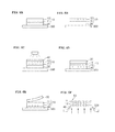
FIGS. 4A to 4F are schematic views illustrating respective steps in a method of manufacturing an LED according to still another embodiment of the present invention.FIGS. 4A to 4F illustrate steps subsequent to the back-grinding step for the LED wafer with the protective sheet, which is obtained through the above-mentioned first embodiment (embodiment illustrated inFIGS. 1A to 1D ). - In this embodiment, as illustrated in
FIGS. 4A and 4B , the LED wafer with the protective sheet, which has been subjected to the back-grinding step, is subjected to the reflective layer forming step. Specifically, the LED wafer with the protective sheet is placed on a table 200 with theprotective sheet 20 side down (FIG. 4A ). After that, areflective layer 40 is formed on the LED wafer on a side opposite to the protective sheet (that is, thesubstrate 12 side) (FIG. 4B ). By forming thereflective layer 40, the amount of light to be extracted from thelight emitting element 11 can be increased. As a material for constituting thereflective layer 40, any appropriate material may be used as long as the light from thelight emitting element 11 may be satisfactorily reflected. Examples of the material for constituting thereflective layer 40 include metals such as aluminum, silver, gold, palladium, platinum, rhodium, and ruthenium. Thereflective layer 40 made of a metal may be formed by, for example, a vapor deposition method (for example, a metal organic chemical vapor deposition method (MOCVD method)). It is preferred that an underlayer formed of, for example, SiO2, TiO2, ZrO2, and/or MgF2 be formed on the surface of theLED wafer 10 on the side opposite to thelight emitting element 11, and then thereflective layer 40 made of a metal be formed by a vapor deposition method. For example, the LED wafer with the protective sheet (LED wafer with the protective sheet formed in the first embodiment) including theprotective sheet 20 on the outer side of thelight emitting element 11 of theLED wafer 10 is subjected to the reflective layer forming step, and thus the metal may be prevented from being deposited on thelight emitting element 11. - After the
reflective layer 40 is formed, as illustrated inFIGS. 4C to 4F , the LED wafer with the protective sheet, which has thereflective layer 40 formed thereon, is subjected to the dicing step. Specifically, the LED wafer with the protective sheet, which has thereflective layer 40 formed thereon, is retained on dicingtape 300 with theprotective sheet 20 side up (FIG. 4C ). After that, theprotective sheet 20 is peeled off (FIG. 4D ). Subsequently, the LED wafer 10 (substantially, the substrate 12) is half-cut in the thickness direction from the exposedlight emitting element 11 side (FIG. 4E ). After that, the dicingtape 300 is expanded so that theLED wafer 10 having thereflective layer 40 formed thereon is split from the cut portion as an origin to obtainLEDs 50 singulated into small element pieces (FIG. 4F ). - Referring to
FIGS. 4E and 4F , description has been made of the embodiment in which theLED wafer 10 is half-cut so as to split the LED wafer from the cut portion as the origin (scribe dicing). InFIG. 4E , theLED wafer 10 is half-cut from thelight emitting element 11 side. However, the dicingtape 300 may be alternatively attached with the substrate 12 (reflective layer 40) side up, and theLED wafer 10 may be half-cut from thesubstrate 12 side (reflective layer 40 side). Further, as a method of cutting the LED wafer, in addition to the above-mentioned scribe dicing, any appropriate method may be adopted. Examples of other methods include a method of cutting theLED wafer 10 in the entire thickness direction to singulate the small element pieces through expanding, and a method of laser cutting only the center portion of theLED wafer 10 in the thickness direction to split theLED wafer 10 from the cut portion as an origin (stealth dicing). - Referring to
FIGS. 4A to 4F , description has been made of the embodiment in which theprotective sheet 20 is not peeled off after the back-grinding step, and the LED wafer with the protective sheet is subjected to the post-process (inFIGS. 4A to 4F , the reflective layer forming step), but the LED wafer may be subjected to the post-process after theprotective sheet 20 is peeled off. It is preferred that, as illustrated inFIGS. 4A to 4F , the LED wafer with the protective sheet be subjected to the post-process. This is because, also in the post-process, the thinned LED wafer can be protected, and the damage to the LED wafer can be prevented. - Referring to
FIGS. 4A to 4F , description has been made of the embodiment in which, prior to the formation of the cut portion for splitting, the reflective layer forming step is performed. The reflective layer forming step may be performed prior to the formation of the cut portion as described above, or may be performed after the cut portion is formed as illustrated inFIGS. 5A to 5F and 6A to 6F. In an embodiment of the present invention illustrated inFIGS. 5A to 5F , the LED wafer with the protective sheet, which has been subjected to the back-grinding step, is retained on the dicingtape 300 with theprotective sheet 20 side up (FIG. 5A ), and after that, theprotective sheet 20 is peeled off (FIG. 5B ). Subsequently, theLED wafer 10 is half-cut from the exposedlight emitting element 11 side (FIG. 5C ). Subsequently, theLED wafer 10 having the cut portion formed therein as described above is subjected to the reflective layer forming step. That is, theLED wafer 10 is placed on the table 200 with thelight emitting element 11 side down, and thereflective layer 40 is formed on thesubstrate 12 side of the LED wafer 10 (FIG. 5D ). Subsequently, theLED wafer 10 having thereflective layer 40 formed thereon is retained on the dicingtape 300 again with the side on which the cut portion is formed (light emitting element 11 side) up (FIG. 5E ). Then, the dicingtape 300 is expanded. Thus, theLED wafer 10 is split from the cut portion as an origin, to thereby obtain theLEDs 50 singulated into small element pieces (FIG. 5F ). - In an embodiment of the present invention illustrated in
FIGS. 6A to 6F , the LED wafer with the protective sheet, which has been subjected to the back-grinding step, is retained on the dicingtape 300 with theprotective sheet 20 side down (FIG. 6A ). Subsequently, theLED wafer 10 is half-cut from thesubstrate 12 side (FIG. 6B ). Subsequently, theLED wafer 10 having the cut portion formed therein as described above is subjected to the reflective layer forming step. That is, theLED wafer 10 is placed on the table 200 with thelight emitting element 11 side (protective sheet 20 side) down, and thereflective layer 40 is formed on thesubstrate 12 side of the LED wafer 10 (FIG. 6C ). TheLED wafer 10 may be placed on the table 200 under a state in which thedicing tape 300 is still adhering on the outer side of theprotective sheet 20, or may be placed on the table 200 after the dicingtape 300 is peeled off (in the illustrated example, theLED wafer 10 is placed after the dicingtape 300 is peeled off). Subsequently, theLED wafer 10 having thereflective layer 40 formed thereon is retained on the dicingtape 300 again with theprotective sheet 20 side up (FIG. 6D ), and then theprotective sheet 20 is peeled off (FIG. 6E ). Then, the dicingtape 300 is expanded. Thus, theLED wafer 10 is split from the cut portion as an origin, to thereby obtain theLEDs 50 singulated into small element pieces (FIG. 6F ). - Regarding the LED wafer with the protective sheet, which is obtained through the above-mentioned second embodiment (embodiment illustrated in
FIGS. 3A to 3D ), in the dicing step, the dicing tape may be attached with the protective sheet side up, and after that, the protective sheet may be peeled off so as to form the cut portion and split the LED wafer. Further, the LED wafer with the protective sheet, which is obtained through the above-mentioned second embodiment, may be subjected to the dicing step after the protective sheet is peeled off. At this time, the dicing tape may be attached to any one of the light emitting element side and the substrate side of the LED wafer. - The LED wafer with the protective sheet, which is obtained through the above-mentioned second embodiment, may be subjected to the reflective layer forming step after the protective sheet is peeled off. The reflective layer forming step may be performed any one of prior to and after the formation of the cut portion, similarly to that performed for the LED wafer obtained through the first embodiment.
Claims (5)
- A method of manufacturing an LED, the method comprising:back-grinding a substrate of an LED wafer including a light emitting element and the substrate; andattaching a protective sheet to the LED wafer one of prior to the back-grinding and after grinding the substrate in the back-grinding.
- A method of manufacturing an LED according to claim 1, wherein the attaching a protective sheet comprises, prior to the back-grinding, attaching the protective sheet on an outer side of the light emitting element of the LED wafer.
- A method of manufacturing an LED according to claim 2, wherein the grinding the substrate in the back-grinding is carried out by attaching the protective sheet to a table via a pressure-sensitive adhesive wax to fix the LED wafer to the table, and
wherein the method further comprises, after the grinding the substrate, taking off the protective sheet to remove, from the LED wafer, the pressure-sensitive adhesive wax adhering on the LED wafer with the protective sheet, which has been released from the table. - A method of manufacturing an LED according to claim 1, wherein the attaching a protective sheet comprises, after the grinding the substrate in the back-grinding, attaching the protective sheet on an outer side of the substrate of the LED wafer.
- A method of manufacturing an LED according to any one of claims 1 to 4, further comprising, after the back-grinding, forming a reflective layer.
Applications Claiming Priority (1)
| Application Number | Priority Date | Filing Date | Title |
|---|---|---|---|
| JP2012145448A JP2014011241A (en) | 2012-06-28 | 2012-06-28 | Led manufacturing method |
Publications (1)
| Publication Number | Publication Date |
|---|---|
| EP2680322A1 true EP2680322A1 (en) | 2014-01-01 |
Family
ID=48577616
Family Applications (1)
| Application Number | Title | Priority Date | Filing Date |
|---|---|---|---|
| EP13171522.9A Withdrawn EP2680322A1 (en) | 2012-06-28 | 2013-06-11 | Method of manufacturing an led |
Country Status (6)
| Country | Link |
|---|---|
| US (1) | US20140004636A1 (en) |
| EP (1) | EP2680322A1 (en) |
| JP (1) | JP2014011241A (en) |
| KR (1) | KR20140001783A (en) |
| CN (1) | CN103531673A (en) |
| TW (1) | TW201409555A (en) |
Families Citing this family (3)
| Publication number | Priority date | Publication date | Assignee | Title |
|---|---|---|---|---|
| JP2015126111A (en) * | 2013-12-26 | 2015-07-06 | 豊田合成株式会社 | Semiconductor element manufacturing method |
| JP6237489B2 (en) * | 2014-06-23 | 2017-11-29 | 住友電気工業株式会社 | Method for manufacturing silicon carbide semiconductor device |
| US9728672B2 (en) * | 2015-02-17 | 2017-08-08 | Genesis Photonics Inc. | Light emitting diode and manufacturing method thereof |
Citations (11)
| Publication number | Priority date | Publication date | Assignee | Title |
|---|---|---|---|---|
| GB2242783A (en) * | 1990-04-06 | 1991-10-09 | Telefunken Electronic Gmbh | Light emitting semiconductor device |
| JP2001044142A (en) * | 1999-07-28 | 2001-02-16 | Seiko Instruments Inc | Silicon wafer cutting method |
| JP2002319708A (en) | 2001-04-23 | 2002-10-31 | Matsushita Electric Works Ltd | Led chip and led device |
| JP2003273042A (en) * | 2002-03-13 | 2003-09-26 | Lintec Corp | Method for manufacturing semiconductor device |
| US20050104081A1 (en) * | 2003-11-18 | 2005-05-19 | Kim Seong-Jin | Semiconductor light emitting diode and method for manufacturing the same |
| JP2005228794A (en) * | 2004-02-10 | 2005-08-25 | Tokyo Seimitsu Co Ltd | Method of manufacturing chip |
| US20060289892A1 (en) * | 2005-06-27 | 2006-12-28 | Lee Jae S | Method for preparing light emitting diode device having heat dissipation rate enhancement |
| EP1791162A1 (en) * | 2005-11-25 | 2007-05-30 | Tokyo Seimitsu Co.,Ltd. | Dicing tape attaching apparatus and dicing tape attaching method |
| JP2007201179A (en) * | 2006-01-26 | 2007-08-09 | Tokyo Seimitsu Co Ltd | Device and method for mounting wafer |
| US20070218651A1 (en) * | 2006-03-14 | 2007-09-20 | Renesas Technology Corp. | Manufacturing method of a semiconductor device |
| US20090230514A1 (en) * | 2007-07-27 | 2009-09-17 | Rohm Co., Ltd. | Method of manufacturing nitride semiconductor device |
Family Cites Families (1)
| Publication number | Priority date | Publication date | Assignee | Title |
|---|---|---|---|---|
| US5994205A (en) * | 1997-02-03 | 1999-11-30 | Kabushiki Kaisha Toshiba | Method of separating semiconductor devices |
-
2012
- 2012-06-28 JP JP2012145448A patent/JP2014011241A/en active Pending
-
2013
- 2013-06-11 EP EP13171522.9A patent/EP2680322A1/en not_active Withdrawn
- 2013-06-13 US US13/917,135 patent/US20140004636A1/en not_active Abandoned
- 2013-06-27 KR KR1020130074524A patent/KR20140001783A/en not_active Withdrawn
- 2013-06-28 TW TW102123364A patent/TW201409555A/en unknown
- 2013-06-28 CN CN201310268247.7A patent/CN103531673A/en active Pending
Patent Citations (12)
| Publication number | Priority date | Publication date | Assignee | Title |
|---|---|---|---|---|
| GB2242783A (en) * | 1990-04-06 | 1991-10-09 | Telefunken Electronic Gmbh | Light emitting semiconductor device |
| JP2001044142A (en) * | 1999-07-28 | 2001-02-16 | Seiko Instruments Inc | Silicon wafer cutting method |
| JP2002319708A (en) | 2001-04-23 | 2002-10-31 | Matsushita Electric Works Ltd | Led chip and led device |
| JP2003273042A (en) * | 2002-03-13 | 2003-09-26 | Lintec Corp | Method for manufacturing semiconductor device |
| US20050104081A1 (en) * | 2003-11-18 | 2005-05-19 | Kim Seong-Jin | Semiconductor light emitting diode and method for manufacturing the same |
| JP2005150675A (en) | 2003-11-18 | 2005-06-09 | Itswell Co Ltd | Semiconductor light emitting diode and manufacturing method thereof |
| JP2005228794A (en) * | 2004-02-10 | 2005-08-25 | Tokyo Seimitsu Co Ltd | Method of manufacturing chip |
| US20060289892A1 (en) * | 2005-06-27 | 2006-12-28 | Lee Jae S | Method for preparing light emitting diode device having heat dissipation rate enhancement |
| EP1791162A1 (en) * | 2005-11-25 | 2007-05-30 | Tokyo Seimitsu Co.,Ltd. | Dicing tape attaching apparatus and dicing tape attaching method |
| JP2007201179A (en) * | 2006-01-26 | 2007-08-09 | Tokyo Seimitsu Co Ltd | Device and method for mounting wafer |
| US20070218651A1 (en) * | 2006-03-14 | 2007-09-20 | Renesas Technology Corp. | Manufacturing method of a semiconductor device |
| US20090230514A1 (en) * | 2007-07-27 | 2009-09-17 | Rohm Co., Ltd. | Method of manufacturing nitride semiconductor device |
Also Published As
| Publication number | Publication date |
|---|---|
| KR20140001783A (en) | 2014-01-07 |
| JP2014011241A (en) | 2014-01-20 |
| CN103531673A (en) | 2014-01-22 |
| US20140004636A1 (en) | 2014-01-02 |
| TW201409555A (en) | 2014-03-01 |
Similar Documents
| Publication | Publication Date | Title |
|---|---|---|
| US20140000793A1 (en) | Method of manufacturing an led | |
| US8541287B2 (en) | Laser processing method for wafer | |
| CN102468233B (en) | Manufacturing method of laser cutting semiconductor wafer | |
| US20140120699A1 (en) | Fabrication method for dicing of semiconductor wafers using laser cutting techniques | |
| JP5146817B2 (en) | Manufacturing method of semiconductor light emitting device | |
| JP5912442B2 (en) | Semiconductor light emitting device and method for manufacturing semiconductor light emitting device | |
| EP2680322A1 (en) | Method of manufacturing an led | |
| CN101320777A (en) | Manufacturing method of LED chip | |
| US20120100695A1 (en) | Manufacturing method of semiconductor device | |
| EP2426741A2 (en) | Semiconductor light emitting device and method of fabricating the same | |
| EP2680325A2 (en) | Method of manufacturing a light emitting diode | |
| US10937927B2 (en) | Group III nitride light-emitting element and method for producing the light-emitting element | |
| JP2012235012A (en) | Light-emitting element and manufacturing method thereof | |
| JP4835409B2 (en) | III-V group semiconductor device and manufacturing method thereof | |
| JP2010267813A (en) | Light emitting device and manufacturing method thereof | |
| US8765504B2 (en) | Semiconductor device structures and the separating methods thereof | |
| CN105895748A (en) | Light-emitting diode and its manufacturing method | |
| EP2680324A1 (en) | Method of manufacturing a LED | |
| US20190019730A1 (en) | Effective compound substrate for non-destructive epitaxial lift-off | |
| JP2014157921A (en) | Semiconductor element and manufacturing method of the same | |
| JP2017117959A (en) | Semiconductor wafer processing method, semiconductor chip manufacturing method, and processed semiconductor wafer | |
| JP2012038758A (en) | Laminated wafer |
Legal Events
| Date | Code | Title | Description |
|---|---|---|---|
| PUAI | Public reference made under article 153(3) epc to a published international application that has entered the european phase |
Free format text: ORIGINAL CODE: 0009012 |
|
| AK | Designated contracting states |
Kind code of ref document: A1 Designated state(s): AL AT BE BG CH CY CZ DE DK EE ES FI FR GB GR HR HU IE IS IT LI LT LU LV MC MK MT NL NO PL PT RO RS SE SI SK SM TR |
|
| AX | Request for extension of the european patent |
Extension state: BA ME |
|
| STAA | Information on the status of an ep patent application or granted ep patent |
Free format text: STATUS: THE APPLICATION IS DEEMED TO BE WITHDRAWN |
|
| 18D | Application deemed to be withdrawn |
Effective date: 20140702 |