EP2680309A1 - Composite substrate, electronic component, and production methods for composite substrate and electronic component - Google Patents
Composite substrate, electronic component, and production methods for composite substrate and electronic component Download PDFInfo
- Publication number
- EP2680309A1 EP2680309A1 EP12750048.6A EP12750048A EP2680309A1 EP 2680309 A1 EP2680309 A1 EP 2680309A1 EP 12750048 A EP12750048 A EP 12750048A EP 2680309 A1 EP2680309 A1 EP 2680309A1
- Authority
- EP
- European Patent Office
- Prior art keywords
- substrate
- silicon
- region
- composite substrate
- amorphous form
- Prior art date
- Legal status (The legal status is an assumption and is not a legal conclusion. Google has not performed a legal analysis and makes no representation as to the accuracy of the status listed.)
- Withdrawn
Links
Images



Classifications
-
- H—ELECTRICITY
- H10—SEMICONDUCTOR DEVICES; ELECTRIC SOLID-STATE DEVICES NOT OTHERWISE PROVIDED FOR
- H10D—INORGANIC ELECTRIC SEMICONDUCTOR DEVICES
- H10D62/00—Semiconductor bodies, or regions thereof, of devices having potential barriers
- H10D62/40—Crystalline structures
-
- H—ELECTRICITY
- H10—SEMICONDUCTOR DEVICES; ELECTRIC SOLID-STATE DEVICES NOT OTHERWISE PROVIDED FOR
- H10D—INORGANIC ELECTRIC SEMICONDUCTOR DEVICES
- H10D62/00—Semiconductor bodies, or regions thereof, of devices having potential barriers
-
- H—ELECTRICITY
- H10—SEMICONDUCTOR DEVICES; ELECTRIC SOLID-STATE DEVICES NOT OTHERWISE PROVIDED FOR
- H10D—INORGANIC ELECTRIC SEMICONDUCTOR DEVICES
- H10D62/00—Semiconductor bodies, or regions thereof, of devices having potential barriers
- H10D62/01—Manufacture or treatment
-
- H—ELECTRICITY
- H10—SEMICONDUCTOR DEVICES; ELECTRIC SOLID-STATE DEVICES NOT OTHERWISE PROVIDED FOR
- H10P—GENERIC PROCESSES OR APPARATUS FOR THE MANUFACTURE OR TREATMENT OF DEVICES COVERED BY CLASS H10
- H10P14/00—Formation of materials, e.g. in the shape of layers or pillars
- H10P14/20—Formation of materials, e.g. in the shape of layers or pillars of semiconductor materials
- H10P14/29—Formation of materials, e.g. in the shape of layers or pillars of semiconductor materials characterised by the substrates
- H10P14/2926—Crystal orientations
-
- H—ELECTRICITY
- H10—SEMICONDUCTOR DEVICES; ELECTRIC SOLID-STATE DEVICES NOT OTHERWISE PROVIDED FOR
- H10P—GENERIC PROCESSES OR APPARATUS FOR THE MANUFACTURE OR TREATMENT OF DEVICES COVERED BY CLASS H10
- H10P90/00—Preparation of wafers not covered by a single main group of this subclass, e.g. wafer reinforcement
- H10P90/19—Preparing inhomogeneous wafers
- H10P90/1904—Preparing vertically inhomogeneous wafers
- H10P90/1906—Preparing SOI wafers
- H10P90/1914—Preparing SOI wafers using bonding
Definitions
- the present invention relates to a composite substrate, an electronic component, and a method of manufacturing a composite substrate and an electronic component.
- a technique for decreasing parasitic capacitance has been developed.
- a silicon-on-sapphire (SOS) structure is known.
- SOS silicon-on-sapphire
- a technique disclosed in Japanese Unexamined Patent Publication JP-A 10-12547 (1998 ) is known.
- the invention has been devised in consideration of the above-described situation, and an object of the invention is to provide a composite substrate having silicon substrate with excellent crystallinity and a method of manufacturing the composite substrate and an electronic component using the composite substrate.
- a composite substrate of the invention includes a support substrate having electrical insulating property, and a silicon substrate which is overlaid on the support substrate, wherein the silicon substrate comprises a plurality of first regions and a second region located between the plurality of first regions, and an amorphous form containing silicon and a metal is present in a main surface of the second region which is located at a side of the support substrate.
- a first method of manufacturing a composite substrate of the invention includes bonding a main surface of a silicon substrate onto a support substrate having electrical insulating property through a metal layer, and heating the support substrate and the silicon substrate bonded with each other to form an amorphous form containing silicon and a metal which forms the metal layer on a main surface of the silicon substrate which is located at a side of the support substrate.
- a second method of manufacturing a composite substrate of the invention includes forming a dent portion in a second region between a plurality of first regions on a main surface of a silicon substrate, forming a metal layer on at least one of the main surface of the silicon substrate and a support substrate having electrical insulating property, bonding the main surface of the silicon substrate onto the support substrate through the metal layer, and heating the support substrate and the silicon substrate bonded with each other configured for aggregating the metal layer in the dent portion and forming an amorphous form containing silicon and a metal which forms the metal layer on the main surface of the silicon substrate which is located at a side of the support substrate.
- a method of manufacturing an electronic component of the invention includes forming a device function unit functioning as a semiconductor device in the plurality of the first regions of the composite substrate, and dividing the composite substrate into regions including at least one of the device function unit.
- An electronic component of the invention includes a support chip and a silicon chip located on the support chip, wherein the silicon chip has a first region in which a device portion functioning as a semiconductor device is provided and a second region which is located surrounding the first region, and an amorphous form containing silicon and a metal is present in a main surface of the second region which is located at a side of the support chip.
- a method of manufacturing an electronic component of the invention includes forming a device function unit functioning as a semiconductor device in the plurality of the first regions of the composite substrate, and dividing the composite substrate into regions including at least one of the device function unit.
- the invention it is possible to provide a composite substrate and an electronic component having a silicon substrate with excellent crystallinity, and a method of manufacturing the composite substrate and the electronic component.
- a composite substrate 1 which is an example of an embodiment of a composite substrate of the invention will be described referring to the drawings.
- the composite substrate 1 shown in Fig. 1 includes a support substrate 10 and a silicon substrate 20.
- the support substrate 10 is a support member of the silicon substrate 20 as a semiconductor layer. It should suffice that the support substrate 10 is electrical insulating, and in this embodiment, the support substrate 10 is formed of aluminum oxide single crystal (hereinafter, referred to as "sapphire"). For the support substrate 10, a silicon carbide substrate or the like may also be used.
- the silicon substrate 20 is overlaid on the main surface (hereinafter, referred to as "top surface 10a") of the support substrate 10 in a D1 direction. In other words, the silicon substrate 20 is supported and bonded directly to the top surface 10a of the support substrate 10.
- the thickness of the support substrate 10 is, for example, in a range of 400 to 800 [ ⁇ m].
- a device function unit which functions as a semiconductor device is formed in a part of the silicon substrate 20.
- silicon single crystal is used as the silicon substrate 20.
- the thickness of the silicon substrate 20 is, for example, in a range of 50 to 300 [nm].
- a region where a device function unit is formed is referred to as a first region 20x
- a region other than the first region 20x is referred to as a second region 20y.
- the first regions 20x are arranged in a matrix, and part of the second region 20y located between the first regions 20x spreads in a lattice shape.
- the second region 20y can be used for splitting or cutting when the composite substrate 1 is divided into desired first regions 20x.
- the formation and arrangement of the first regions 20x are not limited to this embodiment, and are appropriately selected.
- the shape of the second region 20y is appropriately selected according to the shape and arrangement of the first regions 20x.
- the silicon substrate 20 includes a main portion 21 and an amorphous form 22.
- the main portion 21 is a region which occupies the main part of the silicon substrate 20, and is formed of silicon single crystal (hereinafter, simply referred to as "silicon").
- the main portion 21 is primarily located in the first region 20x.
- the amorphous form 22 is a region where the main portion 21 and a metal material are mixed. Examples of the metal material contained in the amorphous form 22 include iron (Fe), nickel (Ni), manganese (Mn), chromium (Cr), and aluminum (Al).
- the amorphous form 22 is primarily located in the second region 20y. That is, the amorphous form 22 is formed between the first regions 20x.
- the amorphous form 22 faces the main surface (hereinafter, referred to as "lower main surface 20b") of the silicon substrate 20 in a D2 direction.
- the amorphous form 22 has a bond of an element forming the main portion 21 and a single metal material.
- the main portion 21 is Si
- the metal material is Fe
- the amorphous form 22 has a Fe-Si bond.
- the amorphous form 22 is not present on the lower main surface 20b, and is present only in the second region 20y. That is, the amorphous form 22 is aggregated, thereby reducing the diffusion depth compared to uniform diffusion. Accordingly, it is possible to suppress the diffusion of the metal material to the silicon substrate 20.
- the amorphous form 22 can be specified by an electronic energy loss spectroscopy (EELS) or the like.
- EELS electronic energy loss spectroscopy
- the interval between a plurality of first regions 20x is equal to or greater than 100 [nm]. More preferably, the interval is equal to or greater than 300 [nm].
- the interval between the plurality of first regions 20x is set as described above, it is possible to eliminate a metal which affects a device function unit to be formed in the first region 20x. The interval between the plurality of first regions 20x will be described below.
- the amorphous form 22 is formed at an inner portion with reference to different surfaces of the silicon substrate 20 except the lower main surface 20b of the silicon substrate 20, that is, a main surface (hereinafter, referred to as "upper main surface 20a") and a lateral surface 20c of the silicon substrate 20 in the D1 and D2 directions.
- the main portion 21 faces the upper main surface 20a and the lateral surface 20c of the silicon substrate 20. That is, the exposed region of the silicon substrate 20 has the same composition. For this reason, in the silicon substrate 20, an effective process can be selected from various processes relating to silicon and appropriately used.
- the amorphous form 22 is arranged surrounding the first region 20x.
- the adhesion strength of sapphire and the amorphous form 22 is greater than the adhesion strength of sapphire and silicon.
- the amorphous form 22 faces the lower main surface 20b of the silicon substrate 20, thereby increasing the adhesion strength of bonding of the support substrate 10 and the silicon substrate 20.
- the configuration of this embodiment may be restated as the individual first region 20x being divided by the amorphous form 22.
- the roughness of the bonded surfaces of the support substrate 10 and the silicon substrate 20 is small, and for example, a mean roughness Ra (arithmetic mean roughness) is smaller than 10 [nm].
- the mean roughness Ra decreases, thereby reducing pressure to be applied when bonding.
- Ra is equal to or smaller than 1 [nm], thereby performing bonding with very small pressure.
- a semiconductor substrate 20X which becomes the silicon substrate 20 is prepared.
- a silicon substrate is adopted as the semiconductor substrate 20X.
- dent portions 20Xd are formed in one main surface which becomes the lower main surface 20b of the silicon substrate 20.
- the dent portion 20Xd is formed in a region which becomes the second region 20y.
- a method of forming the dent portion 20Xd for example, a method in which silicon is partially oxidized using a photomask to selectively remove silicon oxide, or a desired portion is etched using a mask is used.
- the oxidization for example, various methods, such as thermal oxidization, solution oxidization, and the like, are adopted.
- etching a chemical method or a physical method, such as an ion beam, is used.
- the mask for example, a metal mask, a photomask, and the like are known and appropriately selected according to an etching method.
- the depth of the dent portion 20Xd is, for example, about 10 [nm]. It is preferable that the depth of the dent portion 20Xd is smaller than the difference between the thickness in the first region 20x and the thickness of a device function unit 23 described below.
- the support substrate 10 and the semiconductor substrate 20X are bonded together through a metal layer 22X.
- a method in which the surfaces to be bonded are activated to perform bonding, and a method in which an electrostatic force is used to perform bonding are used.
- a method in which an ion beam is irradiated in vacuum to etch and activate the surfaces, or the like is used. It is preferable that the bonding is performed at normal temperature. During the bonding, a method in which a resin-based adhesive is not used is adopted, and bonding is performed by solid state bonding using an atomic force or the like.
- the metal material which forms the metal layer 22X for example, Fe, Cr, Ni, Mn, Al, and Cu may be used alone or in combination.
- the metal material is supplied to the activated surfaces by activating a metal supply source in a bonding apparatus simultaneously with irradiation of an ion beam during bonding.
- the thickness of the metal layer 22X is not particularly limited, and is, for example, equal to or smaller than 5 [nm].
- the metal layer 22X may be in a state where metal elements (particles) are stuck, that is, in a network shape.
- the metal layer 22X is present on the bonding interface when the surfaces are activated and bonded, and in general SOI, since thermal compression bonding is performed through an oxide, it is not even necessary to provide the metal layer.
- the semiconductor substrate 20X is thinned so as to have a desired thickness.
- various methods such as abrasive-grain polishing, chemical etching, and ion beam etching, can be adopted, and multiple methods may be combined.
- the surface of the semiconductor substrate 20X may be smoothened by precise etching along with the thinning.
- etching means using precise etching for example, dry etching is used.
- the dry etching includes dry etching by chemical reaction and dry etching by physical collision.
- dry etching using chemical reaction dry etching using reactive gas, ions and ion beams, or radicals is used.
- etching gas which is used for reactive ions sulfur hexafluoride (SF 6 ), carbon tetrafluoride (CF 4 ), or the like is used.
- dry etching by physical collision dry etching using ion beams is used.
- the dry etching using ion beams includes a method using a gas cluster ion beam (GCIB).
- GCIB gas cluster ion beam
- the support substrate 10 and the semiconductor substrate 20X bonded with each other are heated for aggregating the metal layer 22X in the dent portion 20Xd.
- the aggregated metal layer 22X is mixed with silicon of the semiconductor substrate 20X, and thus the amorphous form 22 is formed. Since silicon of the semiconductor substrate 20X is used in forming the amorphous form 22, the shape of the dent portion 20Xd of the semiconductor substrate 20X changes. That is, a corner portion or a smoothed portion constituting the dent portion 20Xd having a rectangular sectional shape is eliminated.
- the dent portion 20Xd has a shape according to the shape of the amorphous form 22 as an aggregate.
- the temperature in the heating condition is equal to or higher than the melting point of each metal, and more preferably, is equal to or higher than an eutectic temperature of the element forming the semiconductor substrate 20X and the metal material.
- a state equal to or higher than 500°C is maintained for 30 minutes or more, thereby aggregating the metal layer in the dent portion 20Xd.
- An atmosphere during heating is not particularly limited, and any one of air, oxygen, nitrogen, inert gas, reductive gas, and the like may be selected.
- the support substrate 10 and the semiconductor substrate 20X are bonded together in vacuum by activating and bonding the surfaces, it is inferred that a cavity is partially generated in the bonding interface.
- a cavity is generated in the bonding interface. It is considered that, through heating after bonding, the metal is molten, moved so as to bury the cavity, and aggregated at a predetermined place. That is, in this embodiment, the dent portion 20Xd is provided at an intended position, thereby controlling the aggregate position of the metal.
- the silicon substrate 20 of the composite substrate 1 includes a plurality of first regions 20x where a device function unit functioning as a semiconductor device is formed, and the second region 20y which is located between the first regions 20x.
- the amorphous form 22 of silicon and metal is provided in the second region 20y.
- the device function unit 23 is formed from the upper main surface 20a side of the obtained composite substrate 1.
- the device function unit 23 is formed in an arbitrary first region 20x.
- various semiconductor device structures are used. In Fig. 3(a) and Figs. 3(b) and 3(c), different locations are shown.
- the composite substrate 1 in which the device function unit 23 is formed is divided, and thus the electronic component 2 is manufactured.
- the composite substrate 1 into the electronic component 2 at least one of the device function unit 23 is included in one electronic component 2.
- the plurality of first regions 20x, and consequently, a plurality of device function units 23 may be included in one electronic component 2.
- At least one of the amorphous form 22 and the amorphous form 22a obtained by dividing the amorphous form 22 is included in one electronic component 2.
- the amorphous form 22 or the divided amorphous form 22a is included in one electronic component 2, thereby satisfactory adhering a support chip 100 and a silicon chip 200 when using as the electronic component 2.
- the amorphous form 22 is formed from the edge of the first region 20x to the edge of the main portion 21, the amorphous form 22 is not limited to this shape.
- an amorphous form 22A may surround the edge of the first region 20x.
- the amorphous form 22 surrounds the first region 20x in a lattice shape
- the amorphous form 22 is not limited to this shape, for example, as a silicon substrate 20B shown in Fig. 5 , a pair of amorphous forms 22B which extend along the first region 20x may be provided.
- amorphous forms 22C may be provided at four corners of the first region 20x.
- the metal layer 22X is aggregated to form the amorphous form 22, a part of the metal layer 22X may form the amorphous form 22, and the other part may be left as the metal layer 22X.
- a part which is left as the metal layer 22X may not have uniform concentration, and the concentration distribution of the metal may be generated.
- the dent portion 20Xd is formed in the silicon substrate 20, and the metal is aggregated in the dent portion 20Xd, the dent portion 20Xd may not be provided.
- the thickness (corresponding to the supply metal amount) of the metal layer 22X to be formed in Fig. 2(c) is adjusted, thereby aggregating the metal layer 22X at a given interval according to the supply metal amount.
- the size of the amorphous form 22 depends on the supply metal amount.
- the interval of the amorphous form 22 can be about 100 [nm].
- the interval of the amorphous form 22 is smaller than 100 [nm], because in this case it is possible to suppress the adverse effect of the size of the amorphous form 22 on the operation characteristics as the electronic component 2. It is preferable that the interval of the amorphous form 22 is equal to or greater than 300 [nm], because in this case it is possible to further reduce the size of the amorphous form 22 and to suppress the adverse effect on the operation characteristics as the electronic component 2. Specifically, it is preferable that the size of the amorphous form 22 in the thickness direction is smaller than the size obtained by subtracting the thickness required to form the semiconductor device function unit 23 from the thickness of the thickness silicon substrate 20.
Landscapes
- Recrystallisation Techniques (AREA)
- Chemical & Material Sciences (AREA)
- Crystallography & Structural Chemistry (AREA)
- Thin Film Transistor (AREA)
- Pressure Welding/Diffusion-Bonding (AREA)
Abstract
Description
- The present invention relates to a composite substrate, an electronic component, and a method of manufacturing a composite substrate and an electronic component.
- In recent years, in order to achieve performance improvement of a semiconductor device, a technique for decreasing parasitic capacitance has been developed. As a technique for decreasing parasitic capacitance, a silicon-on-sapphire (SOS) structure is known. As a method of forming the SOS structure, for example, a technique disclosed in Japanese Unexamined Patent Publication
JP-A 10-12547 (1998 - However, in the technique disclosed in
JP-A 10-12547 (1998 - The invention has been devised in consideration of the above-described situation, and an object of the invention is to provide a composite substrate having silicon substrate with excellent crystallinity and a method of manufacturing the composite substrate and an electronic component using the composite substrate.
- A composite substrate of the invention includes a support substrate having electrical insulating property, and a silicon substrate which is overlaid on the support substrate, wherein the silicon substrate comprises a plurality of first regions and a second region located between the plurality of first regions, and an amorphous form containing silicon and a metal is present in a main surface of the second region which is located at a side of the support substrate.
- A first method of manufacturing a composite substrate of the invention includes bonding a main surface of a silicon substrate onto a support substrate having electrical insulating property through a metal layer, and heating the support substrate and the silicon substrate bonded with each other to form an amorphous form containing silicon and a metal which forms the metal layer on a main surface of the silicon substrate which is located at a side of the support substrate.
- A second method of manufacturing a composite substrate of the invention includes forming a dent portion in a second region between a plurality of first regions on a main surface of a silicon substrate, forming a metal layer on at least one of the main surface of the silicon substrate and a support substrate having electrical insulating property, bonding the main surface of the silicon substrate onto the support substrate through the metal layer, and heating the support substrate and the silicon substrate bonded with each other configured for aggregating the metal layer in the dent portion and forming an amorphous form containing silicon and a metal which forms the metal layer on the main surface of the silicon substrate which is located at a side of the support substrate.
- A method of manufacturing an electronic component of the invention includes forming a device function unit functioning as a semiconductor device in the plurality of the first regions of the composite substrate, and dividing the composite substrate into regions including at least one of the device function unit.
- An electronic component of the invention includes a support chip and a silicon chip located on the support chip, wherein the silicon chip has a first region in which a device portion functioning as a semiconductor device is provided and a second region which is located surrounding the first region, and an amorphous form containing silicon and a metal is present in a main surface of the second region which is located at a side of the support chip.
- A method of manufacturing an electronic component of the invention includes forming a device function unit functioning as a semiconductor device in the plurality of the first regions of the composite substrate, and dividing the composite substrate into regions including at least one of the device function unit.
- According to the invention, it is possible to provide a composite substrate and an electronic component having a silicon substrate with excellent crystallinity, and a method of manufacturing the composite substrate and the electronic component.
-
-
Fig. 1(a) is a plan view showing the schematic configuration of an embodiment of a composite substrate according to the invention, andFig. 1(b) is a sectional view taken along the line Ib-Ib ofFig. 1(a) ; -
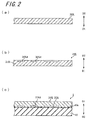
Figs. 2(a) to 2(c) are schematic views showing an embodiment of a process for manufacturing a composite substrate and a semiconductor device according to the invention; -
Figs. 3(a) to 3(c) are schematic views showing a process subsequent toFig. 2 ; -
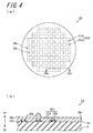
Fig. 4(a) is a plan view showing the schematic configuration of a modified example of the composite substrate shown inFig. 1 , andFig. 4(b) is a sectional view taken along the line IVb-IVb ofFig. 4(a) ; -
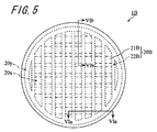
Fig. 5 is a plan view showing the schematic configuration of a modified example of the composite substrate shown inFig. 1 ; -
Fig. 6(a) is a sectional view taken along the line VIa-VIa ofFig. 5 , andFig. 6(b) is a sectional view taken along the line VIb-VIb ofFig. 5 ; -
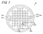
Fig. 7 is a plan view showing the schematic configuration of a modified example of the composite substrate shown inFig. 1 ; and -
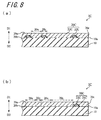
Fig. 8(a) is a sectional view taken along the line VIIIa-VIIIa ofFig. 7 , andFig. 8(b) is a sectional view taken along the line VIIIb-VIIIb ofFig. 7 - A
composite substrate 1 which is an example of an embodiment of a composite substrate of the invention will be described referring to the drawings. Thecomposite substrate 1 shown inFig. 1 includes asupport substrate 10 and asilicon substrate 20. - The
support substrate 10 is a support member of thesilicon substrate 20 as a semiconductor layer. It should suffice that thesupport substrate 10 is electrical insulating, and in this embodiment, thesupport substrate 10 is formed of aluminum oxide single crystal (hereinafter, referred to as "sapphire"). For thesupport substrate 10, a silicon carbide substrate or the like may also be used. Thesilicon substrate 20 is overlaid on the main surface (hereinafter, referred to as "top surface 10a") of thesupport substrate 10 in a D1 direction. In other words, thesilicon substrate 20 is supported and bonded directly to thetop surface 10a of thesupport substrate 10. The thickness of thesupport substrate 10 is, for example, in a range of 400 to 800 [µm]. - A device function unit which functions as a semiconductor device is formed in a part of the
silicon substrate 20. In this embodiment, silicon single crystal is used as thesilicon substrate 20. The thickness of thesilicon substrate 20 is, for example, in a range of 50 to 300 [nm]. In thesilicon substrate 20, a region where a device function unit is formed is referred to as afirst region 20x, and a region other than thefirst region 20x is referred to as asecond region 20y. Thefirst regions 20x are arranged in a matrix, and part of thesecond region 20y located between thefirst regions 20x spreads in a lattice shape. Thesecond region 20y can be used for splitting or cutting when thecomposite substrate 1 is divided into desiredfirst regions 20x. The formation and arrangement of thefirst regions 20x are not limited to this embodiment, and are appropriately selected. The shape of thesecond region 20y is appropriately selected according to the shape and arrangement of thefirst regions 20x. - The
silicon substrate 20 includes amain portion 21 and anamorphous form 22. Themain portion 21 is a region which occupies the main part of thesilicon substrate 20, and is formed of silicon single crystal (hereinafter, simply referred to as "silicon"). Themain portion 21 is primarily located in thefirst region 20x. Theamorphous form 22 is a region where themain portion 21 and a metal material are mixed. Examples of the metal material contained in theamorphous form 22 include iron (Fe), nickel (Ni), manganese (Mn), chromium (Cr), and aluminum (Al). Theamorphous form 22 is primarily located in thesecond region 20y. That is, theamorphous form 22 is formed between thefirst regions 20x. Theamorphous form 22 faces the main surface (hereinafter, referred to as "lowermain surface 20b") of thesilicon substrate 20 in a D2 direction. - The
amorphous form 22 has a bond of an element forming themain portion 21 and a single metal material. When themain portion 21 is Si, and the metal material is Fe, theamorphous form 22 has a Fe-Si bond. Theamorphous form 22 is not present on the lowermain surface 20b, and is present only in thesecond region 20y. That is, theamorphous form 22 is aggregated, thereby reducing the diffusion depth compared to uniform diffusion. Accordingly, it is possible to suppress the diffusion of the metal material to thesilicon substrate 20. - The
amorphous form 22 can be specified by an electronic energy loss spectroscopy (EELS) or the like. - It is preferable that the interval between a plurality of
first regions 20x is equal to or greater than 100 [nm]. More preferably, the interval is equal to or greater than 300 [nm]. When a metal is present between a region directly below a portion where a device function unit is formed and thesupport substrate 10, device characteristics may be deteriorated. Meanwhile, the interval between the plurality offirst regions 20x is set as described above, it is possible to eliminate a metal which affects a device function unit to be formed in thefirst region 20x. The interval between the plurality offirst regions 20x will be described below. - The
amorphous form 22 is formed at an inner portion with reference to different surfaces of thesilicon substrate 20 except the lowermain surface 20b of thesilicon substrate 20, that is, a main surface (hereinafter, referred to as "uppermain surface 20a") and alateral surface 20c of thesilicon substrate 20 in the D1 and D2 directions. In other words, themain portion 21 faces the uppermain surface 20a and thelateral surface 20c of thesilicon substrate 20. That is, the exposed region of thesilicon substrate 20 has the same composition. For this reason, in thesilicon substrate 20, an effective process can be selected from various processes relating to silicon and appropriately used. - The
amorphous form 22 is arranged surrounding thefirst region 20x. The adhesion strength of sapphire and theamorphous form 22 is greater than the adhesion strength of sapphire and silicon. Theamorphous form 22 faces the lowermain surface 20b of thesilicon substrate 20, thereby increasing the adhesion strength of bonding of thesupport substrate 10 and thesilicon substrate 20. In thecomposite substrate 1, even after thecomposite substrate 1 is divided as a semiconductor device, it is possible to satisfactorily adhere thesupport substrate 10 and thesilicon substrate 20. The configuration of this embodiment may be restated as the individualfirst region 20x being divided by theamorphous form 22. - It is preferable that the roughness of the bonded surfaces of the
support substrate 10 and thesilicon substrate 20 is small, and for example, a mean roughness Ra (arithmetic mean roughness) is smaller than 10 [nm]. The mean roughness Ra decreases, thereby reducing pressure to be applied when bonding. In particular, Ra is equal to or smaller than 1 [nm], thereby performing bonding with very small pressure. - An example of an embodiment of a method of manufacturing a composite substrate and a semiconductor device of the invention will be described referring to
Figs. 2 to 4 . - First, as shown in
Fig. 2(a) , asemiconductor substrate 20X which becomes thesilicon substrate 20 is prepared. In this embodiment, a silicon substrate is adopted as thesemiconductor substrate 20X. - Next, as shown in
Fig. 2(b) , in the main surface of thesemiconductor substrate 20X, dent portions 20Xd are formed in one main surface which becomes the lowermain surface 20b of thesilicon substrate 20. The dent portion 20Xd is formed in a region which becomes thesecond region 20y. As a method of forming the dent portion 20Xd, for example, a method in which silicon is partially oxidized using a photomask to selectively remove silicon oxide, or a desired portion is etched using a mask is used. As the oxidization, for example, various methods, such as thermal oxidization, solution oxidization, and the like, are adopted. As etching, a chemical method or a physical method, such as an ion beam, is used. As the mask, for example, a metal mask, a photomask, and the like are known and appropriately selected according to an etching method. - It should suffice that the depth of the dent portion 20Xd is, for example, about 10 [nm]. It is preferable that the depth of the dent portion 20Xd is smaller than the difference between the thickness in the
first region 20x and the thickness of adevice function unit 23 described below. - Next, as shown in
Fig. 2(c) , thesupport substrate 10 and thesemiconductor substrate 20X are bonded together through ametal layer 22X. As the bonding method, a method in which the surfaces to be bonded are activated to perform bonding, and a method in which an electrostatic force is used to perform bonding are used. As the method of activating the surfaces, for example, a method in which an ion beam is irradiated in vacuum to etch and activate the surfaces, or the like is used. It is preferable that the bonding is performed at normal temperature. During the bonding, a method in which a resin-based adhesive is not used is adopted, and bonding is performed by solid state bonding using an atomic force or the like. - As the metal material which forms the
metal layer 22X, for example, Fe, Cr, Ni, Mn, Al, and Cu may be used alone or in combination. The metal material is supplied to the activated surfaces by activating a metal supply source in a bonding apparatus simultaneously with irradiation of an ion beam during bonding. The thickness of themetal layer 22X is not particularly limited, and is, for example, equal to or smaller than 5 [nm]. Themetal layer 22X may be in a state where metal elements (particles) are stuck, that is, in a network shape. Themetal layer 22X is present on the bonding interface when the surfaces are activated and bonded, and in general SOI, since thermal compression bonding is performed through an oxide, it is not even necessary to provide the metal layer. - Next, the
semiconductor substrate 20X is thinned so as to have a desired thickness. As the thinning method, various methods, such as abrasive-grain polishing, chemical etching, and ion beam etching, can be adopted, and multiple methods may be combined. - The surface of the
semiconductor substrate 20X may be smoothened by precise etching along with the thinning. As etching means using precise etching, for example, dry etching is used. The dry etching includes dry etching by chemical reaction and dry etching by physical collision. As the dry etching using chemical reaction, dry etching using reactive gas, ions and ion beams, or radicals is used. As etching gas which is used for reactive ions, sulfur hexafluoride (SF6), carbon tetrafluoride (CF4), or the like is used. As dry etching by physical collision, dry etching using ion beams is used. The dry etching using ion beams includes a method using a gas cluster ion beam (GCIB). Thesemiconductor substrate 20X is scanned with a movable stage while etching a narrow region using the etching means, thereby satisfactorily performing precise etching even on a large-area material substrate. - Next, the
support substrate 10 and thesemiconductor substrate 20X bonded with each other are heated for aggregating themetal layer 22X in the dent portion 20Xd. The aggregatedmetal layer 22X is mixed with silicon of thesemiconductor substrate 20X, and thus theamorphous form 22 is formed. Since silicon of thesemiconductor substrate 20X is used in forming theamorphous form 22, the shape of the dent portion 20Xd of thesemiconductor substrate 20X changes. That is, a corner portion or a smoothed portion constituting the dent portion 20Xd having a rectangular sectional shape is eliminated. The dent portion 20Xd has a shape according to the shape of theamorphous form 22 as an aggregate. - The temperature in the heating condition is equal to or higher than the melting point of each metal, and more preferably, is equal to or higher than an eutectic temperature of the element forming the
semiconductor substrate 20X and the metal material. For example, in this embodiment, a state equal to or higher than 500°C is maintained for 30 minutes or more, thereby aggregating the metal layer in the dent portion 20Xd. An atmosphere during heating is not particularly limited, and any one of air, oxygen, nitrogen, inert gas, reductive gas, and the like may be selected. - As in this embodiment, when the
support substrate 10 and thesemiconductor substrate 20X are bonded together in vacuum by activating and bonding the surfaces, it is inferred that a cavity is partially generated in the bonding interface. In particular, in this example, since the dent portion 20Xd is provided, in normal-temperature bonding by activating the bonded surfaces, a cavity is generated in the bonding interface. It is considered that, through heating after bonding, the metal is molten, moved so as to bury the cavity, and aggregated at a predetermined place. That is, in this embodiment, the dent portion 20Xd is provided at an intended position, thereby controlling the aggregate position of the metal. - As described above, it is possible to obtain the
composite substrate 1 in which thesilicon substrate 20 is bonded onto thesupport substrate 10 having electrical insulation. Thesilicon substrate 20 of thecomposite substrate 1 includes a plurality offirst regions 20x where a device function unit functioning as a semiconductor device is formed, and thesecond region 20y which is located between thefirst regions 20x. In thesemiconductor substrate 20 of thecomposite substrate 1, theamorphous form 22 of silicon and metal is provided in thesecond region 20y. - Next, as shown in
Fig. 3(b) , thedevice function unit 23 is formed from the uppermain surface 20a side of the obtainedcomposite substrate 1. Thedevice function unit 23 is formed in an arbitraryfirst region 20x. As thedevice function unit 23, various semiconductor device structures are used. InFig. 3(a) and Figs. 3(b) and 3(c), different locations are shown. - Next, as shown in
Fig. 3(c) , thecomposite substrate 1 in which thedevice function unit 23 is formed is divided, and thus theelectronic component 2 is manufactured. When dividing thecomposite substrate 1 into theelectronic component 2, at least one of thedevice function unit 23 is included in oneelectronic component 2. In other words, the plurality offirst regions 20x, and consequently, a plurality ofdevice function units 23 may be included in oneelectronic component 2. - At least one of the
amorphous form 22 and theamorphous form 22a obtained by dividing theamorphous form 22 is included in oneelectronic component 2. Theamorphous form 22 or the dividedamorphous form 22a is included in oneelectronic component 2, thereby satisfactory adhering asupport chip 100 and asilicon chip 200 when using as theelectronic component 2. - In this way, it is possible to manufacture the
electronic component 2 having thedevice function unit 23. - The invention is not limited to the foregoing embodiment, and it should be noted that various variations may be made without departing from the scope of the invention.
- For example, although in the
silicon substrate 20, theamorphous form 22 is formed from the edge of thefirst region 20x to the edge of themain portion 21, theamorphous form 22 is not limited to this shape. For example, as asilicon substrate 20A shown inFig. 4 , anamorphous form 22A may surround the edge of thefirst region 20x. - In the
silicon substrate 20, although theamorphous form 22 surrounds thefirst region 20x in a lattice shape, theamorphous form 22 is not limited to this shape, for example, as asilicon substrate 20B shown inFig. 5 , a pair ofamorphous forms 22B which extend along thefirst region 20x may be provided. As asilicon substrate 20C shown inFig. 6 ,amorphous forms 22C may be provided at four corners of thefirst region 20x. - In the above-described manufacturing method, although the
metal layer 22X is aggregated to form theamorphous form 22, a part of themetal layer 22X may form theamorphous form 22, and the other part may be left as themetal layer 22X. A part which is left as themetal layer 22X may not have uniform concentration, and the concentration distribution of the metal may be generated. - In the above-described manufacturing method, as shown in
Fig. 2(b) , although the dent portion 20Xd is formed in thesilicon substrate 20, and the metal is aggregated in the dent portion 20Xd, the dent portion 20Xd may not be provided. In this case, the thickness (corresponding to the supply metal amount) of themetal layer 22X to be formed inFig. 2(c) is adjusted, thereby aggregating themetal layer 22X at a given interval according to the supply metal amount. Similarly, the size of theamorphous form 22 depends on the supply metal amount. - For example, when the metal supply amount is 1×10¹⁶ [atoms/cm3], the interval of the
amorphous form 22 can be about 100 [nm]. - From the relationship between the metal supply amount and the interval of the
amorphous form 22, it is preferable that the interval of theamorphous form 22 is smaller than 100 [nm], because in this case it is possible to suppress the adverse effect of the size of theamorphous form 22 on the operation characteristics as theelectronic component 2. It is preferable that the interval of theamorphous form 22 is equal to or greater than 300 [nm], because in this case it is possible to further reduce the size of theamorphous form 22 and to suppress the adverse effect on the operation characteristics as theelectronic component 2. Specifically, it is preferable that the size of theamorphous form 22 in the thickness direction is smaller than the size obtained by subtracting the thickness required to form the semiconductordevice function unit 23 from the thickness of thethickness silicon substrate 20. -
- 1, 1A to 1C:
- Composite substrate
- 2:
- Electronic component
- 10:
- Support substrate
- 10a:
- Top surface
- 20, 20A to 20C:
- Semiconductor layer
- 20a:
- Upper main surface
- 20b:
- Lower main surface
- 20c:
- Lateral surface
- 20x:
- First region
- 20y:
- Second region
- 20X:
- Semiconductor substrate
- 20Xd:
- Dent portion
- 21, 21A to 21C:
- Main portion
- 22, 22A to 22C:
- Amorphous form
- 22a:
- Divided amorphous form
- 22X:
- Metal layer
- 23:
- Device function unit
Claims (13)
- A composite substrate, comprising:a support substrate having electrical insulating property; anda silicon substrate which is overlaid on the support substrate, whereinthe silicon substrate comprises a plurality of first regions and a second region located between the plurality of first regions, andan amorphous form containing silicon and a metal is present in a main surface of the second region which is located at a side of the support substrate.
- The composite substrate according to claim 1,
wherein the support substrate is single crystal predominantly composed of aluminum oxide. - The composite substrate according to claim 1 or 2,
wherein the amorphous form surrounds the plurality of first regions. - The composite substrate according to any one of claims 1 to 3,
wherein the amorphous form is located at an inner portion with reference to surfaces of the silicon substrate except the main surface of the silicon substrate located at the side of the support substrate. - The composite substrate according to any one of claims 1 to 3,
wherein the amorphous form is located at an inner portion with reference to a lateral surface of the silicon substrate. - The composite substrate according to claim 1,
wherein the plurality of first regions are arranged at an interval equal to or greater than 100 nm. - The composite substrate according to claim 1,
wherein the plurality of first regions are arranged at an interval equal to or greater than 300 nm. - A method of manufacturing a composite substrate, comprising:bonding a main surface of a silicon substrate onto a support substrate having electrical insulating property through a metal layer; andheating the support substrate and the silicon substrate bonded with each other to form an amorphous form containing silicon and a metal which forms the metal layer on a main surface of the silicon substrate which is located at a side of the support substrate.
- A method of manufacturing a composite substrate, comprising:forming a dent portion in a second region between a plurality of first regions on a main surface of a silicon substrate;forming a metal layer on at least one of the main surface of the silicon substrate and a support substrate having electrical insulating property;bonding the main surface of the silicon substrate onto the support substrate through the metal layer; andheating the support substrate and the silicon substrate bonded with each other configured for aggregating the metal layer in the dent portion and forming an amorphous form containing silicon and a metal which forms the metal layer on the main surface of the silicon substrate which is located at a side of the support substrate.
- A method of manufacturing an electronic component, comprising:forming a device function unit functioning as a semiconductor device in the plurality of the first regions of the composite substrate according to claim 1; anddividing the composite substrate into regions including at least one of the device function unit.
- The method of manufacturing an electronic component according to claim 10,
wherein, in dividing the composite substrate, the composite substrate is divided such that the second region is exposed in a divided surface formed by dividing the composite substrate. - An electronic component, comprising:a support chip having electrical insulating property; anda silicon chip located on the support chip, whereinthe silicon chip has a first region in which a device portion functioning as a semiconductor device is provided and a second region which is located surrounding the first region, andan amorphous form containing silicon and a metal is present in a main surface of the second region which is locate at a side of the support chip.
- The electronic component according to claim 12,
wherein the second region is located on an entire outer lateral surface of the silicon chip.
Applications Claiming Priority (2)
| Application Number | Priority Date | Filing Date | Title |
|---|---|---|---|
| JP2011039334 | 2011-02-25 | ||
| PCT/JP2012/054796 WO2012115269A1 (en) | 2011-02-25 | 2012-02-27 | Composite substrate, electronic component, and production methods for composite substrate and electronic component |
Publications (2)
| Publication Number | Publication Date |
|---|---|
| EP2680309A1 true EP2680309A1 (en) | 2014-01-01 |
| EP2680309A4 EP2680309A4 (en) | 2014-09-17 |
Family
ID=46721036
Family Applications (1)
| Application Number | Title | Priority Date | Filing Date |
|---|---|---|---|
| EP12750048.6A Withdrawn EP2680309A4 (en) | 2011-02-25 | 2012-02-27 | COMPOSITE SUBSTRATE, ELECTRONIC COMPONENT, AND METHODS OF MANUFACTURING COMPOSITE SUBSTRATE AND ELECTRONIC COMPONENT |
Country Status (4)
| Country | Link |
|---|---|
| US (1) | US9245942B2 (en) |
| EP (1) | EP2680309A4 (en) |
| JP (1) | JP5460871B2 (en) |
| WO (1) | WO2012115269A1 (en) |
Families Citing this family (2)
| Publication number | Priority date | Publication date | Assignee | Title |
|---|---|---|---|---|
| JP5926401B2 (en) * | 2013-05-31 | 2016-05-25 | 京セラ株式会社 | Composite substrate and manufacturing method thereof |
| WO2015046483A1 (en) * | 2013-09-30 | 2015-04-02 | 京セラ株式会社 | Composite substrate and method for producing same |
Family Cites Families (6)
| Publication number | Priority date | Publication date | Assignee | Title |
|---|---|---|---|---|
| JPH084126B2 (en) | 1987-09-19 | 1996-01-17 | 富士通株式会社 | Method for manufacturing semiconductor device |
| JPH1012547A (en) | 1996-06-19 | 1998-01-16 | Asahi Chem Ind Co Ltd | Method of manufacturing semiconductor substrate |
| US6423614B1 (en) | 1998-06-30 | 2002-07-23 | Intel Corporation | Method of delaminating a thin film using non-thermal techniques |
| US6524935B1 (en) | 2000-09-29 | 2003-02-25 | International Business Machines Corporation | Preparation of strained Si/SiGe on insulator by hydrogen induced layer transfer technique |
| FR2864336B1 (en) * | 2003-12-23 | 2006-04-28 | Commissariat Energie Atomique | METHOD FOR SEALING TWO PLATES WITH FORMATION OF AN OHMIC CONTACT BETWEEN THEM |
| JP2009010140A (en) * | 2007-06-27 | 2009-01-15 | Oki Electric Ind Co Ltd | Semiconductor wafer |
-
2012
- 2012-02-27 JP JP2012524029A patent/JP5460871B2/en not_active Expired - Fee Related
- 2012-02-27 WO PCT/JP2012/054796 patent/WO2012115269A1/en not_active Ceased
- 2012-02-27 US US14/001,411 patent/US9245942B2/en active Active
- 2012-02-27 EP EP12750048.6A patent/EP2680309A4/en not_active Withdrawn
Also Published As
| Publication number | Publication date |
|---|---|
| JP5460871B2 (en) | 2014-04-02 |
| EP2680309A4 (en) | 2014-09-17 |
| JPWO2012115269A1 (en) | 2014-07-07 |
| WO2012115269A1 (en) | 2012-08-30 |
| US20130328048A1 (en) | 2013-12-12 |
| US9245942B2 (en) | 2016-01-26 |
Similar Documents
| Publication | Publication Date | Title |
|---|---|---|
| KR101299719B1 (en) | Process for fabricating a multilayer structure with trimming using thermo-mechanical effects | |
| US7608521B2 (en) | Producing SOI structure using high-purity ion shower | |
| JP5319764B2 (en) | Incremental trimming | |
| KR100743557B1 (en) | Multilayer structures having controlled internal stresses and methods of making such structures | |
| JP4425631B2 (en) | Method for manufacturing a thin film layer containing microcomponents | |
| KR101185426B1 (en) | A mixed trimming method | |
| US8420506B2 (en) | Process for cleaving a substrate | |
| KR20030093359A (en) | Thin films and production methods thereof | |
| US12151314B2 (en) | Device and method for applying pressure to stress-producing layers for improved guidance of a separation crack | |
| JPH1197379A (en) | Semiconductor substrate and method of manufacturing semiconductor substrate | |
| TW201527061A (en) | Combined manufacturing method for separating one solid matter into a plurality of solid layers | |
| KR20120112533A (en) | Manufacturing method of bonded wafer | |
| CN111092148A (en) | Method for manufacturing piezoelectric material composite substrate | |
| CN113725160B (en) | Ultra-thin wafer front side cutting process | |
| US9245942B2 (en) | Composite substrate, electronic component, and method of manufacturing composite substrate and electronic component | |
| JP3864495B2 (en) | Manufacturing method of semiconductor substrate | |
| JP4611227B2 (en) | Manufacturing method of composite wafer structure | |
| JP2005129676A (en) | Silicon substrate for SOI substrate, SOI substrate, and method for manufacturing the SOI substrate | |
| JP3754818B2 (en) | Method for manufacturing semiconductor substrate | |
| KR20070096942A (en) | Gettering method and wafer using same | |
| EP2156466B1 (en) | Method for separating a semiconductor wafer into individual semiconductor dies using an implanted impurity | |
| JP2007173694A (en) | Method for manufacturing semiconductor substrate | |
| JP2006303201A (en) | Process for producing soi substrate | |
| EP3370249A1 (en) | Bonded soi wafer manufacturing method | |
| US20130119519A1 (en) | Composite substrate, electronic component, and method for manufacturing composite substrate, and method for manufacturing electronic component |
Legal Events
| Date | Code | Title | Description |
|---|---|---|---|
| PUAI | Public reference made under article 153(3) epc to a published international application that has entered the european phase |
Free format text: ORIGINAL CODE: 0009012 |
|
| 17P | Request for examination filed |
Effective date: 20130925 |
|
| AK | Designated contracting states |
Kind code of ref document: A1 Designated state(s): AL AT BE BG CH CY CZ DE DK EE ES FI FR GB GR HR HU IE IS IT LI LT LU LV MC MK MT NL NO PL PT RO RS SE SI SK SM TR |
|
| DAX | Request for extension of the european patent (deleted) | ||
| A4 | Supplementary search report drawn up and despatched |
Effective date: 20140818 |
|
| RIC1 | Information provided on ipc code assigned before grant |
Ipc: H01L 21/02 20060101ALI20140811BHEP Ipc: H01L 27/12 20060101AFI20140811BHEP Ipc: H01L 21/20 20060101ALI20140811BHEP |
|
| STAA | Information on the status of an ep patent application or granted ep patent |
Free format text: STATUS: THE APPLICATION IS DEEMED TO BE WITHDRAWN |
|
| 18D | Application deemed to be withdrawn |
Effective date: 20150317 |