EP2679536B1 - Anodically bonded strain isolator - Google Patents
Anodically bonded strain isolator Download PDFInfo
- Publication number
- EP2679536B1 EP2679536B1 EP13171937.9A EP13171937A EP2679536B1 EP 2679536 B1 EP2679536 B1 EP 2679536B1 EP 13171937 A EP13171937 A EP 13171937A EP 2679536 B1 EP2679536 B1 EP 2679536B1
- Authority
- EP
- European Patent Office
- Prior art keywords
- layer
- mems die
- mems
- spring
- bonding
- Prior art date
- Legal status (The legal status is an assumption and is not a legal conclusion. Google has not performed a legal analysis and makes no representation as to the accuracy of the status listed.)
- Not-in-force
Links
Images


Classifications
-
- B—PERFORMING OPERATIONS; TRANSPORTING
- B81—MICROSTRUCTURAL TECHNOLOGY
- B81B—MICROSTRUCTURAL DEVICES OR SYSTEMS, e.g. MICROMECHANICAL DEVICES
- B81B7/00—Microstructural systems; Auxiliary parts of microstructural devices or systems
- B81B7/0032—Packages or encapsulation
- B81B7/0045—Packages or encapsulation for reducing stress inside of the package structure
- B81B7/0051—Packages or encapsulation for reducing stress inside of the package structure between the package lid and the substrate
Definitions
- Inertial and pressure sensors can be very sensitive to stresses and strains, interpreting the stresses/strains as signals when, in fact, they are not. These errors are often seen over temperature because the strain state of the system, to which the sensors are mounted, changes with expansion and contraction, due to temperature change. Other sources of strain change are also significant enough to have a negative effect on sensors, such as creep under stress or pressure. Changes in output over temperature must be modeled and subtracted from a sensor's output where accuracy is required. Larger strains from a given temperature change are harder to model accurately and may require more computing power and higher-order models. Any relaxation (creep) of the materials due to these strains cannot be modeled and shows up as sensor error.
- EP 2246292 discloses a package into faceplate for mechanical isolation of micro electromechanical system (MEMS) structures wherein flexible beams are configured to deflect under stress such that effects on the sensor die of a thermal mismatch are reduced.
- MEMS micro electromechanical system
- US 2009/0261691 discloses a MEMS device and method for manufacturing in which strains on semiconductor substrate are reduced by avoiding an internal line or side surface line.
- Mechanical isolators are often used between the sensor and the system to which the sensor is mounted to allow for the strains to be taken up by the isolator rather than passing them on to the sensor.
- the isolator does this by having a mechanically elastic section between the sensor mount and the system, like a set of springs that always comes back to the same state after being stretched. Isolation features are easy to form in certain materials, such as silicon, but sensors are often made of other materials and the bond between the sensor and isolator creates unwanted stresses.
- the present invention in its various aspects is as set out in the appended claims.
- the present invention provides a stress isolator that allows a sensor to be attached to materials of the same coefficient of thermal expansion and still provide the required elastic isolation between the sensor and the system to which it is mounted. It does this using microelectromechanical system (MEMS) processing methods and is particularly compatible with MEMS sensors.
- MEMS microelectromechanical system
- the isolator is made of two materials, borosilicate glass and silicon.
- the glass is the same material as the mounting surface of the MEMS sensors.
- the silicon makes an excellent isolator, being very elastic and easy to form into complex shapes.
- the two materials of the isolator are joined using an anodic bond.
- the construction of the isolator can be specific to different types of MEMS sensors, making the most of their geometry to reduce overall volume.
- the isolator supports other electrical components necessary to the MEMS sensor, which reduces overall system volume and increases performance by making the electrical paths as short as possible.
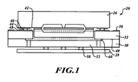
- FIGURE 1 shows an exemplary microelectromechanical system (MEMS) package 20 that is mounted to a circuit board or housing 28.
- the MEMS package 20 includes an isolator having a spring layer 30 made of silicon or similar material and a glass layer 32.
- a frame of the spring layer 30 is bonded (i.e., anodically) to the glass layer 32.
- the glass layer 32 is bonded to a glass section of the MEMS die 26.
- the MEMS die 26 includes a flange (or cutout) 42 formed by the removal of portions of a cover and device layer.
- the flange 42 is made of glass similar to that of the glass layer 32.
- the flange 42 is attached to the glass layer 32 using metal pads 46, 48 (as necessary) and gold (or comparable metal) stud bumps 44.
- a hole that was previously etched or machined into the glass layer 32 allows reception of a portion of the MEMS die 26 that has been mounted in a flip-chip manner.
- a raft 52 of the silicon spring layer 30 is mounted to the housing 28 using gold (or comparable metal) stud bumps 58.
- a recess 60 is etched into the spring layer 30 prior to being bonded with the glass layer 32.
- Other suitable, electrically conductive attachment methods may be used for attaching the MEMS die 26 to the glass layer 32 or the spring layer 30 to the circuit board 28, such as solder, gold-silicon eutectic, or epoxy.
- the isolator is a perfect or near-perfect coefficient of thermal expansion (CTE) match with the MEMS die 26.
- the spring layer 30 provides zero or near-zero outgassing and is easily formable into intricate shapes for the proper balance of support and flexibility required to absorb stress, using various photolithography techniques, various isotropic and nonisotropic etchants, and plasma-based techniques, such as deep reactive ion etching.
- the MEMS die 26 includes a section of borosilicate glass.
- the silicon is also a close CTE match to the MEMS die glass.
- metal patterns are applied to a first surface of a glass wafer, then hole(s) are drilled through the glass wafer.
- a potassium hydroxide (KOH) etch is performed on a front side of a silicon wafer to create the recess 60.
- a deep reactive ion etch (DRIE) is performed through the silicon wafer from a back side to create spring structures.
- the glass wafer is anodically bonded to the silicon wafer.
- the MEMS sensor is bonded to the isolator, then the isolator is attached to a MEMS package.
- the MEMS sensors 26 is bonded to the isolator as a full wafer before dicing or one MEMS sensor at a time is bonded to one isolator after both the isolator wafer and MEMS wafer are diced.
- the isolator allows for mounting of support electronics as close to the MEMS device as is possible. This allows for the least noise and smallest power consumption.
- various kinds of surface-mount electrical devices, in die or packaged form, can be mounted.
- FIGURE 2-1 shows a top perspective view of an exemplary isolator glass layer 32-1 that has been etched to provide a window that is framed on two opposing sides by flanges 64.
- Metallized pads 48-1 have been applied to a top surface of the flanges 64.
- Other pads 50-1 and traces (not shown) are simultaneously applied to the top surface of the isolator glass layer 32-1 for flip-chip mounting of a MEMS die.
- the interconnect traces are not shown, for clarity, and could connect in any required form.
- FIGURE 2-2 shows a recess 60-1 located on a bottom of isolator glass layer 32-1.
- the recess 60-1 can be applied, instead of the recess 60, on the spring layer 30 of FIGURE 1 .
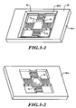
- FIGURE 3-1 shows a top perspective view of an exemplary spring layer 30-1.
- the spring layer 30-1 includes a frame 68 with a window 66. Etched into the window 66 are four S-shaped springs 72 and a raft 70. The springs 72 attach at one end to a different interior edge of the window 66 and at a second end to a different exterior edge of the raft 70.
- FIGURE 3-2 shows an optional metal pad 74 that is attached to an underside of the raft 70. The metal pad 74 is later used to mount to a circuit board or housing via stud bumps (such as are shown in FIGURE 1 ) or other suitable attachment methods such as solder, gold-silicon eutectic, or epoxy.
- a recess 60-2 is etched around the top edge of the window 66.
- FIGURE 4 shows a bottom perspective view of an exemplary MEMS die 26-1 configured to attach to the isolator glass layer 32-1 shown in FIGURES 2-1, 2-2 .
- Flanges 42-1 have been formed from one end of the MEMS die 26-1, such that the flanges 42-1 reside near an intermediate section of the MEMS die 26-1.
- Metalized pads 46-1 are either applied to the flanges 42-1 or are previously applied to an intermediate/device layer of the MEMS die 26-1 and become exposed upon removal of material of the section adjacent the intermediate/device layer.
- the metallized pads 46-1 electrically connect to active components within the MEMS die 26-1.
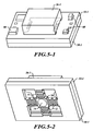
- FIGURES 5-1 and 5-2 show the isolator glass layer 32-1 bonded to the spring layer 30-1 and the MEMS die 26-1 bonded to the isolator glass layer 32-1.
- the metalized pads 48-1 and 46-1 are bonded together, using stud bumps (not shown), in order to attach the MEMS die 26-1 to the isolator glass layer 32-1.
- electrical components 80 are attached to the metallized pads 50-1.
- An example of the connection between the metalized pads 48-1, 46-1 and their respective surfaces are SiAu eutectic bonds.
- the MEMS die is mounted face up. Leads on the MEMS die are wirebonded to metal pads on the isolator or directly out to the circuit board/package. In another embodiment, the MEMS die has pads on its top surface and is flip-chip mounted to the glass on the isolator. A low-stress electrical connection from the isolator glass is then made, such as wirebonds.
Landscapes
- Engineering & Computer Science (AREA)
- Microelectronics & Electronic Packaging (AREA)
- Computer Hardware Design (AREA)
- Pressure Sensors (AREA)
- Micromachines (AREA)
Description
- Inertial and pressure sensors can be very sensitive to stresses and strains, interpreting the stresses/strains as signals when, in fact, they are not. These errors are often seen over temperature because the strain state of the system, to which the sensors are mounted, changes with expansion and contraction, due to temperature change. Other sources of strain change are also significant enough to have a negative effect on sensors, such as creep under stress or pressure. Changes in output over temperature must be modeled and subtracted from a sensor's output where accuracy is required. Larger strains from a given temperature change are harder to model accurately and may require more computing power and higher-order models. Any relaxation (creep) of the materials due to these strains cannot be modeled and shows up as sensor error.
-
EP 2246292 discloses a package into faceplate for mechanical isolation of micro electromechanical system (MEMS) structures wherein flexible beams are configured to deflect under stress such that effects on the sensor die of a thermal mismatch are reduced.US 2009/0261691 discloses a MEMS device and method for manufacturing in which strains on semiconductor substrate are reduced by avoiding an internal line or side surface line. - Mechanical isolators are often used between the sensor and the system to which the sensor is mounted to allow for the strains to be taken up by the isolator rather than passing them on to the sensor. The isolator does this by having a mechanically elastic section between the sensor mount and the system, like a set of springs that always comes back to the same state after being stretched. Isolation features are easy to form in certain materials, such as silicon, but sensors are often made of other materials and the bond between the sensor and isolator creates unwanted stresses.
- The present invention in its various aspects is as set out in the appended claims. The present invention provides a stress isolator that allows a sensor to be attached to materials of the same coefficient of thermal expansion and still provide the required elastic isolation between the sensor and the system to which it is mounted. It does this using microelectromechanical system (MEMS) processing methods and is particularly compatible with MEMS sensors. The isolator is made of two materials, borosilicate glass and silicon. The glass is the same material as the mounting surface of the MEMS sensors. The silicon makes an excellent isolator, being very elastic and easy to form into complex shapes. The two materials of the isolator are joined using an anodic bond. The construction of the isolator can be specific to different types of MEMS sensors, making the most of their geometry to reduce overall volume.
- In one aspect of the invention, the isolator supports other electrical components necessary to the MEMS sensor, which reduces overall system volume and increases performance by making the electrical paths as short as possible.
- Preferred and alternative embodiments of the present invention are described in detail below with reference to the following drawings:
-
FIGURE 1 is a side view of a MEMS package formed in accordance with an embodiment of the present invention; -
FIGURES 2-1 and 2-2 are perspective views of an exemplary glass layer for use in a MEMS package, such as is shown inFIGURE 1 ; -
FIGURES 3-1 and 3-2 are perspective views of an exemplary spring layer for use in a MEMS package, such as is shown inFIGURE 1 ; -
FIGURE 4 is a perspective view of an exemplary MEMS component for mounting to the glass layer shown inFIGURES 2-1 and 2-2 ; and -
FIGURES 5-1 and 5-2 are perspective views of the combined components fromFIGURES 2 through 4 . -
FIGURE 1 shows an exemplary microelectromechanical system (MEMS)package 20 that is mounted to a circuit board orhousing 28. In one embodiment, the MEMSpackage 20 includes an isolator having aspring layer 30 made of silicon or similar material and aglass layer 32. A frame of thespring layer 30 is bonded (i.e., anodically) to theglass layer 32. Then, theglass layer 32 is bonded to a glass section of theMEMS die 26. - In one embodiment, the MEMS die 26 includes a flange (or cutout) 42 formed by the removal of portions of a cover and device layer. The
flange 42 is made of glass similar to that of theglass layer 32. Theflange 42 is attached to theglass layer 32 usingmetal pads 46, 48 (as necessary) and gold (or comparable metal)stud bumps 44. A hole that was previously etched or machined into theglass layer 32 allows reception of a portion of theMEMS die 26 that has been mounted in a flip-chip manner. A raft 52 of thesilicon spring layer 30 is mounted to thehousing 28 using gold (or comparable metal)stud bumps 58. A recess 60 is etched into thespring layer 30 prior to being bonded with theglass layer 32. Other suitable, electrically conductive attachment methods may be used for attaching theMEMS die 26 to theglass layer 32 or thespring layer 30 to thecircuit board 28, such as solder, gold-silicon eutectic, or epoxy. - The isolator is a perfect or near-perfect coefficient of thermal expansion (CTE) match with the
MEMS die 26. Thespring layer 30 provides zero or near-zero outgassing and is easily formable into intricate shapes for the proper balance of support and flexibility required to absorb stress, using various photolithography techniques, various isotropic and nonisotropic etchants, and plasma-based techniques, such as deep reactive ion etching. The MEMS die 26 includes a section of borosilicate glass. The silicon is also a close CTE match to the MEMS die glass. - The following describes an exemplary construction process. First, metal patterns are applied to a first surface of a glass wafer, then hole(s) are drilled through the glass wafer. Next, a potassium hydroxide (KOH) etch is performed on a front side of a silicon wafer to create the recess 60. Then, a deep reactive ion etch (DRIE) is performed through the silicon wafer from a back side to create spring structures. Then, the glass wafer is anodically bonded to the silicon wafer. Next, the MEMS sensor is bonded to the isolator, then the isolator is attached to a MEMS package. In one embodiment, the
MEMS sensors 26 is bonded to the isolator as a full wafer before dicing or one MEMS sensor at a time is bonded to one isolator after both the isolator wafer and MEMS wafer are diced. - The isolator allows for mounting of support electronics as close to the MEMS device as is possible. This allows for the least noise and smallest power consumption. By properly patterning metal on the
glass layer 32, various kinds of surface-mount electrical devices, in die or packaged form, can be mounted. -
FIGURE 2-1 shows a top perspective view of an exemplary isolator glass layer 32-1 that has been etched to provide a window that is framed on two opposing sides by flanges 64. Metallized pads 48-1 have been applied to a top surface of the flanges 64. Other pads 50-1 and traces (not shown) are simultaneously applied to the top surface of the isolator glass layer 32-1 for flip-chip mounting of a MEMS die. The interconnect traces are not shown, for clarity, and could connect in any required form.FIGURE 2-2 shows a recess 60-1 located on a bottom of isolator glass layer 32-1. The recess 60-1 can be applied, instead of the recess 60, on thespring layer 30 ofFIGURE 1 . -
FIGURE 3-1 shows a top perspective view of an exemplary spring layer 30-1. The spring layer 30-1 includes aframe 68 with awindow 66. Etched into thewindow 66 are four S-shaped springs 72 and araft 70. Thesprings 72 attach at one end to a different interior edge of thewindow 66 and at a second end to a different exterior edge of theraft 70.FIGURE 3-2 shows anoptional metal pad 74 that is attached to an underside of theraft 70. Themetal pad 74 is later used to mount to a circuit board or housing via stud bumps (such as are shown inFIGURE 1 ) or other suitable attachment methods such as solder, gold-silicon eutectic, or epoxy. A recess 60-2 is etched around the top edge of thewindow 66. -
FIGURE 4 shows a bottom perspective view of an exemplary MEMS die 26-1 configured to attach to the isolator glass layer 32-1 shown inFIGURES 2-1, 2-2 . Flanges 42-1 have been formed from one end of the MEMS die 26-1, such that the flanges 42-1 reside near an intermediate section of the MEMS die 26-1. Metalized pads 46-1 are either applied to the flanges 42-1 or are previously applied to an intermediate/device layer of the MEMS die 26-1 and become exposed upon removal of material of the section adjacent the intermediate/device layer. The metallized pads 46-1 electrically connect to active components within the MEMS die 26-1. -
FIGURES 5-1 and 5-2 show the isolator glass layer 32-1 bonded to the spring layer 30-1 and the MEMS die 26-1 bonded to the isolator glass layer 32-1. The metalized pads 48-1 and 46-1 are bonded together, using stud bumps (not shown), in order to attach the MEMS die 26-1 to the isolator glass layer 32-1. Also,electrical components 80 are attached to the metallized pads 50-1. An example of the connection between the metalized pads 48-1, 46-1 and their respective surfaces are SiAu eutectic bonds. - In one embodiment, the MEMS die is mounted face up. Leads on the MEMS die are wirebonded to metal pads on the isolator or directly out to the circuit board/package. In another embodiment, the MEMS die has pads on its top surface and is flip-chip mounted to the glass on the isolator. A low-stress electrical connection from the isolator glass is then made, such as wirebonds.
Claims (10)
- A microelectromechanical system (MEMS) package (20) comprising:a MEMS die (26) comprising:a sensor; anda bonding portion (42); andan isolation apparatus comprising:a first layer (32) configured to bond to the bonding portion of the MEMS die, the first layer having a coefficient of thermal expansion approximately equal to the bonding portion of the MEMS die; anda spring layer (30) formed of a monolithic material, the spring layer comprising:a first section (68) configured to bond to the first layer;a second section (52, 70) configured to bond to a circuit board (28); andone or more spring elements (72) configured to flexibly attach the first section to the second section;wherein a bond between the first layer and the spring layer comprises an anodic bond.
- The package of Claim 1, wherein the first layer and the bonding portion of the MEMS die comprise glass.
- The package of Claim 2, wherein the isolation apparatus further comprises:at least one metal pad (48, 50) bonded to the first layer;at least one metal pad (46) bonded to the MEMS die; andat least one electrically conductive bonding material (44) bonded between the at least one first layer metal pad and the at least one MEMS die metal pad,wherein the at least one MEMS die metal pad is electrically coupled to internal components of the MEMS die.
- The package of Claim 1, wherein the first layer comprises a cavity configured to allow the MEMS die to pass through when the MEMS die is mounted to the first layer, wherein the cavity comprises at least one flange configured to bond to only the MEMS die., wherein at least one of the first layer or the spring layer comprises a recess (60) configured to provide separation of the at least one flange from the spring layer.
- The package of Claim 1, wherein the spring layer comprises silicon and the first layer comprises glass.
- A method for providing a microelectromechanical system (MEMS) package of any of claims 1 to 5, the method comprising:anodically bonding a first layer (32) to a first section (68) of a spring layer (30);bonding the first layer (32) to a bonding portion (42) of a MEMS die (26), the first layer having a coefficient of thermal expansion approximately equal to the bonding portion of the MEMS die; andbonding a second section (52, 70) of the spring layer (30) to a circuit board (28),wherein the spring layer comprises one or more spring elements (72) that flexibly attach the first section to the second section.
- The method of Claim 6, wherein the first layer and the bonding portion of the MEMS die comprise glass.
- The method of Claim 7, wherein bonding the first layer to the bonding portion of the MEMS die comprises:bonding at least one metal pad (48, 50) to the first layer;bonding at least one metal pad (46) to the MEMS die; andbounding at least one electrically conductive bonding material (44) between the at least one first layer metal pad and the at least one MEMS die metal pad,wherein the at least one MEMS die metal pad is electrically coupled to internal components of the MEMS die.
- The method of Claim 6, further comprising etching a cavity into the first layer to allow the MEMS die to pass through when the MEMS die is mounted to the first layer.
- The method of Claim 9, further comprising etching a recess (60) into at least one of the first layer or the spring layer to provide separation of the at least one flange from the spring layer.
Priority Applications (1)
| Application Number | Priority Date | Filing Date | Title |
|---|---|---|---|
| EP15163575.2A EP2915778B1 (en) | 2012-06-26 | 2013-06-13 | Anodically bonded strain isolator |
Applications Claiming Priority (1)
| Application Number | Priority Date | Filing Date | Title |
|---|---|---|---|
| US13/533,356 US9187313B2 (en) | 2012-06-26 | 2012-06-26 | Anodically bonded strain isolator |
Related Child Applications (1)
| Application Number | Title | Priority Date | Filing Date |
|---|---|---|---|
| EP15163575.2A Division EP2915778B1 (en) | 2012-06-26 | 2013-06-13 | Anodically bonded strain isolator |
Publications (3)
| Publication Number | Publication Date |
|---|---|
| EP2679536A2 EP2679536A2 (en) | 2014-01-01 |
| EP2679536A3 EP2679536A3 (en) | 2014-01-22 |
| EP2679536B1 true EP2679536B1 (en) | 2015-04-15 |
Family
ID=48655969
Family Applications (2)
| Application Number | Title | Priority Date | Filing Date |
|---|---|---|---|
| EP15163575.2A Not-in-force EP2915778B1 (en) | 2012-06-26 | 2013-06-13 | Anodically bonded strain isolator |
| EP13171937.9A Not-in-force EP2679536B1 (en) | 2012-06-26 | 2013-06-13 | Anodically bonded strain isolator |
Family Applications Before (1)
| Application Number | Title | Priority Date | Filing Date |
|---|---|---|---|
| EP15163575.2A Not-in-force EP2915778B1 (en) | 2012-06-26 | 2013-06-13 | Anodically bonded strain isolator |
Country Status (3)
| Country | Link |
|---|---|
| US (1) | US9187313B2 (en) |
| EP (2) | EP2915778B1 (en) |
| JP (1) | JP2014004681A (en) |
Families Citing this family (13)
| Publication number | Priority date | Publication date | Assignee | Title |
|---|---|---|---|---|
| US20130264755A1 (en) * | 2012-04-05 | 2013-10-10 | Honeywell International Inc. | Methods and systems for limiting sensor motion |
| US20140374847A1 (en) * | 2013-06-20 | 2014-12-25 | Honeywell International Inc. | Packaging method for mems devices |
| EP2871456B1 (en) * | 2013-11-06 | 2018-10-10 | Invensense, Inc. | Pressure sensor and method for manufacturing a pressure sensor |
| CN105182004A (en) * | 2015-09-06 | 2015-12-23 | 苏州大学 | Silicon-silicon bonding based micro mechanical accelerometer for reducing packaging stress |
| FR3042483B1 (en) | 2015-10-16 | 2017-11-24 | Thales Sa | ELECTROMECHANICAL MICROSYSTEM AND METHOD OF MANUFACTURE |
| US10278281B1 (en) * | 2015-10-30 | 2019-04-30 | Garmin International, Inc. | MEMS stress isolation and stabilization system |
| US10060820B2 (en) * | 2015-12-22 | 2018-08-28 | Continental Automotive Systems, Inc. | Stress-isolated absolute pressure sensor |
| EP3243793B1 (en) * | 2016-05-10 | 2018-11-07 | ams AG | Sensor assembly and arrangement and method for manufacturing a sensor assembly |
| US10442680B2 (en) * | 2016-06-14 | 2019-10-15 | Mems Drive, Inc. | Electric connection flexures |
| GB2555412A (en) | 2016-10-25 | 2018-05-02 | Atlantic Inertial Systems Ltd | Inertial sensor |
| FR3075772B1 (en) | 2017-12-22 | 2020-11-20 | Commissariat Energie Atomique | IMPLEMENTATION OF A DECOUPLING STRUCTURE FOR THE ASSEMBLY OF A COMPONENT WITH A BOX |
| US10988375B1 (en) | 2018-10-04 | 2021-04-27 | EngeniusMicro, LLC | Systems, methods, and devices for mechanical isolation or mechanical damping of microfabricated inertial sensors |
| US20230391609A1 (en) * | 2022-06-03 | 2023-12-07 | International Business Machines Corporation | Micromachined superconducting interconnect in silicon |
Family Cites Families (2)
| Publication number | Priority date | Publication date | Assignee | Title |
|---|---|---|---|---|
| WO2008023465A1 (en) * | 2006-08-25 | 2008-02-28 | Kyocera Corporation | Microelectronic machine mechanism device, and its manufacturing method |
| US8614491B2 (en) | 2009-04-07 | 2013-12-24 | Honeywell International Inc. | Package interface plate for package isolation structures |
-
2012
- 2012-06-26 US US13/533,356 patent/US9187313B2/en active Active
-
2013
- 2013-06-13 EP EP15163575.2A patent/EP2915778B1/en not_active Not-in-force
- 2013-06-13 EP EP13171937.9A patent/EP2679536B1/en not_active Not-in-force
- 2013-06-20 JP JP2013129309A patent/JP2014004681A/en not_active Withdrawn
Also Published As
| Publication number | Publication date |
|---|---|
| EP2679536A2 (en) | 2014-01-01 |
| EP2915778B1 (en) | 2016-11-02 |
| JP2014004681A (en) | 2014-01-16 |
| EP2915778A1 (en) | 2015-09-09 |
| US9187313B2 (en) | 2015-11-17 |
| EP2679536A3 (en) | 2014-01-22 |
| US20130341735A1 (en) | 2013-12-26 |
Similar Documents
| Publication | Publication Date | Title |
|---|---|---|
| EP2679536B1 (en) | Anodically bonded strain isolator | |
| US7402905B2 (en) | Methods of fabrication of wafer-level vacuum packaged devices | |
| EP2423656B1 (en) | Pressure sensor | |
| EP1785392B1 (en) | Miniature package for translation of sensor sense axis | |
| US9061888B2 (en) | Sensor module and method for producing sensor modules | |
| US20060163679A1 (en) | High performance MEMS packaging architecture | |
| US20070164378A1 (en) | Integrated mems package | |
| EP2816005A2 (en) | Packaging method for MEMS devices for reducing thermal stress | |
| US9499398B2 (en) | Vertically hybridly integrated assembly having an interposer for stress-decoupling of a MEMS structure, and method for its manufacture | |
| JP2009241164A (en) | Semiconductor sensor apparatus and manufacturing method therefor | |
| US11012790B2 (en) | Flipchip package | |
| US20080099861A1 (en) | Sensor device package having thermally compliant die pad | |
| EP2617677B1 (en) | Structure for isolating a microstructure die from packaging stress | |
| EP3260831B1 (en) | Low cost small force sensor | |
| EP2319798B1 (en) | MEMS package having electrical connections for edge mount | |
| Lee et al. | A generic environment-resistant packaging technology for MEMS | |
| JP2013154465A (en) | Mems device assembly and method of packaging the same | |
| WO2013006167A1 (en) | Sensor die | |
| JP2003028892A (en) | Acceleration sensor | |
| US10723615B2 (en) | Sensor assembly and arrangement and method for manufacturing a sensor assembly | |
| Dean et al. | Micromachined LCP for packaging MEMS sensors | |
| CN117566682A (en) | Stress isolation packaging structure of MEMS device | |
| Fontana et al. | Holed packaging for mems sensors | |
| JP2007178374A (en) | Semiconductor device and manufacturing method of the same | |
| CN113443602A (en) | Wafer level packaging structure of micro electro mechanical system chip and manufacturing process thereof |
Legal Events
| Date | Code | Title | Description |
|---|---|---|---|
| PUAL | Search report despatched |
Free format text: ORIGINAL CODE: 0009013 |
|
| PUAI | Public reference made under article 153(3) epc to a published international application that has entered the european phase |
Free format text: ORIGINAL CODE: 0009012 |
|
| 17P | Request for examination filed |
Effective date: 20130613 |
|
| AK | Designated contracting states |
Kind code of ref document: A2 Designated state(s): AL AT BE BG CH CY CZ DE DK EE ES FI FR GB GR HR HU IE IS IT LI LT LU LV MC MK MT NL NO PL PT RO RS SE SI SK SM TR |
|
| AX | Request for extension of the european patent |
Extension state: BA ME |
|
| AK | Designated contracting states |
Kind code of ref document: A3 Designated state(s): AL AT BE BG CH CY CZ DE DK EE ES FI FR GB GR HR HU IE IS IT LI LT LU LV MC MK MT NL NO PL PT RO RS SE SI SK SM TR |
|
| AX | Request for extension of the european patent |
Extension state: BA ME |
|
| RIC1 | Information provided on ipc code assigned before grant |
Ipc: B81B 7/00 20060101AFI20131217BHEP |
|
| 17Q | First examination report despatched |
Effective date: 20140311 |
|
| GRAP | Despatch of communication of intention to grant a patent |
Free format text: ORIGINAL CODE: EPIDOSNIGR1 |
|
| INTG | Intention to grant announced |
Effective date: 20141208 |
|
| GRAS | Grant fee paid |
Free format text: ORIGINAL CODE: EPIDOSNIGR3 |
|
| GRAA | (expected) grant |
Free format text: ORIGINAL CODE: 0009210 |
|
| AK | Designated contracting states |
Kind code of ref document: B1 Designated state(s): AL AT BE BG CH CY CZ DE DK EE ES FI FR GB GR HR HU IE IS IT LI LT LU LV MC MK MT NL NO PL PT RO RS SE SI SK SM TR |
|
| REG | Reference to a national code |
Ref country code: GB Ref legal event code: FG4D Ref country code: CH Ref legal event code: EP |
|
| REG | Reference to a national code |
Ref country code: FR Ref legal event code: PLFP Year of fee payment: 3 |
|
| REG | Reference to a national code |
Ref country code: IE Ref legal event code: FG4D |
|
| REG | Reference to a national code |
Ref country code: AT Ref legal event code: REF Ref document number: 721844 Country of ref document: AT Kind code of ref document: T Effective date: 20150515 |
|
| REG | Reference to a national code |
Ref country code: DE Ref legal event code: R096 Ref document number: 602013001497 Country of ref document: DE Effective date: 20150528 |
|
| REG | Reference to a national code |
Ref country code: NL Ref legal event code: VDEP Effective date: 20150415 |
|
| REG | Reference to a national code |
Ref country code: AT Ref legal event code: MK05 Ref document number: 721844 Country of ref document: AT Kind code of ref document: T Effective date: 20150415 |
|
| REG | Reference to a national code |
Ref country code: LT Ref legal event code: MG4D |
|
| PG25 | Lapsed in a contracting state [announced via postgrant information from national office to epo] |
Ref country code: NL Free format text: LAPSE BECAUSE OF FAILURE TO SUBMIT A TRANSLATION OF THE DESCRIPTION OR TO PAY THE FEE WITHIN THE PRESCRIBED TIME-LIMIT Effective date: 20150415 |
|
| PG25 | Lapsed in a contracting state [announced via postgrant information from national office to epo] |
Ref country code: NO Free format text: LAPSE BECAUSE OF FAILURE TO SUBMIT A TRANSLATION OF THE DESCRIPTION OR TO PAY THE FEE WITHIN THE PRESCRIBED TIME-LIMIT Effective date: 20150715 Ref country code: ES Free format text: LAPSE BECAUSE OF FAILURE TO SUBMIT A TRANSLATION OF THE DESCRIPTION OR TO PAY THE FEE WITHIN THE PRESCRIBED TIME-LIMIT Effective date: 20150415 Ref country code: PT Free format text: LAPSE BECAUSE OF FAILURE TO SUBMIT A TRANSLATION OF THE DESCRIPTION OR TO PAY THE FEE WITHIN THE PRESCRIBED TIME-LIMIT Effective date: 20150817 Ref country code: LT Free format text: LAPSE BECAUSE OF FAILURE TO SUBMIT A TRANSLATION OF THE DESCRIPTION OR TO PAY THE FEE WITHIN THE PRESCRIBED TIME-LIMIT Effective date: 20150415 Ref country code: FI Free format text: LAPSE BECAUSE OF FAILURE TO SUBMIT A TRANSLATION OF THE DESCRIPTION OR TO PAY THE FEE WITHIN THE PRESCRIBED TIME-LIMIT Effective date: 20150415 Ref country code: HR Free format text: LAPSE BECAUSE OF FAILURE TO SUBMIT A TRANSLATION OF THE DESCRIPTION OR TO PAY THE FEE WITHIN THE PRESCRIBED TIME-LIMIT Effective date: 20150415 |
|
| PG25 | Lapsed in a contracting state [announced via postgrant information from national office to epo] |
Ref country code: AT Free format text: LAPSE BECAUSE OF FAILURE TO SUBMIT A TRANSLATION OF THE DESCRIPTION OR TO PAY THE FEE WITHIN THE PRESCRIBED TIME-LIMIT Effective date: 20150415 Ref country code: IS Free format text: LAPSE BECAUSE OF FAILURE TO SUBMIT A TRANSLATION OF THE DESCRIPTION OR TO PAY THE FEE WITHIN THE PRESCRIBED TIME-LIMIT Effective date: 20150815 Ref country code: LV Free format text: LAPSE BECAUSE OF FAILURE TO SUBMIT A TRANSLATION OF THE DESCRIPTION OR TO PAY THE FEE WITHIN THE PRESCRIBED TIME-LIMIT Effective date: 20150415 Ref country code: RS Free format text: LAPSE BECAUSE OF FAILURE TO SUBMIT A TRANSLATION OF THE DESCRIPTION OR TO PAY THE FEE WITHIN THE PRESCRIBED TIME-LIMIT Effective date: 20150415 Ref country code: GR Free format text: LAPSE BECAUSE OF FAILURE TO SUBMIT A TRANSLATION OF THE DESCRIPTION OR TO PAY THE FEE WITHIN THE PRESCRIBED TIME-LIMIT Effective date: 20150716 |
|
| RAP2 | Party data changed (patent owner data changed or rights of a patent transferred) |
Owner name: HONEYWELL INTERNATIONAL INC. |
|
| REG | Reference to a national code |
Ref country code: DE Ref legal event code: R097 Ref document number: 602013001497 Country of ref document: DE |
|
| PG25 | Lapsed in a contracting state [announced via postgrant information from national office to epo] |
Ref country code: EE Free format text: LAPSE BECAUSE OF FAILURE TO SUBMIT A TRANSLATION OF THE DESCRIPTION OR TO PAY THE FEE WITHIN THE PRESCRIBED TIME-LIMIT Effective date: 20150415 Ref country code: DK Free format text: LAPSE BECAUSE OF FAILURE TO SUBMIT A TRANSLATION OF THE DESCRIPTION OR TO PAY THE FEE WITHIN THE PRESCRIBED TIME-LIMIT Effective date: 20150415 Ref country code: IT Free format text: LAPSE BECAUSE OF FAILURE TO SUBMIT A TRANSLATION OF THE DESCRIPTION OR TO PAY THE FEE WITHIN THE PRESCRIBED TIME-LIMIT Effective date: 20150415 Ref country code: MC Free format text: LAPSE BECAUSE OF FAILURE TO SUBMIT A TRANSLATION OF THE DESCRIPTION OR TO PAY THE FEE WITHIN THE PRESCRIBED TIME-LIMIT Effective date: 20150415 |
|
| PLBE | No opposition filed within time limit |
Free format text: ORIGINAL CODE: 0009261 |
|
| STAA | Information on the status of an ep patent application or granted ep patent |
Free format text: STATUS: NO OPPOSITION FILED WITHIN TIME LIMIT |
|
| PG25 | Lapsed in a contracting state [announced via postgrant information from national office to epo] |
Ref country code: CZ Free format text: LAPSE BECAUSE OF FAILURE TO SUBMIT A TRANSLATION OF THE DESCRIPTION OR TO PAY THE FEE WITHIN THE PRESCRIBED TIME-LIMIT Effective date: 20150415 Ref country code: RO Free format text: LAPSE BECAUSE OF NON-PAYMENT OF DUE FEES Effective date: 20150415 Ref country code: LU Free format text: LAPSE BECAUSE OF FAILURE TO SUBMIT A TRANSLATION OF THE DESCRIPTION OR TO PAY THE FEE WITHIN THE PRESCRIBED TIME-LIMIT Effective date: 20150613 Ref country code: SK Free format text: LAPSE BECAUSE OF FAILURE TO SUBMIT A TRANSLATION OF THE DESCRIPTION OR TO PAY THE FEE WITHIN THE PRESCRIBED TIME-LIMIT Effective date: 20150415 Ref country code: PL Free format text: LAPSE BECAUSE OF FAILURE TO SUBMIT A TRANSLATION OF THE DESCRIPTION OR TO PAY THE FEE WITHIN THE PRESCRIBED TIME-LIMIT Effective date: 20150415 |
|
| 26N | No opposition filed |
Effective date: 20160118 |
|
| REG | Reference to a national code |
Ref country code: IE Ref legal event code: MM4A |
|
| PG25 | Lapsed in a contracting state [announced via postgrant information from national office to epo] |
Ref country code: IE Free format text: LAPSE BECAUSE OF NON-PAYMENT OF DUE FEES Effective date: 20150613 |
|
| PG25 | Lapsed in a contracting state [announced via postgrant information from national office to epo] |
Ref country code: SI Free format text: LAPSE BECAUSE OF FAILURE TO SUBMIT A TRANSLATION OF THE DESCRIPTION OR TO PAY THE FEE WITHIN THE PRESCRIBED TIME-LIMIT Effective date: 20150415 |
|
| REG | Reference to a national code |
Ref country code: FR Ref legal event code: PLFP Year of fee payment: 4 |
|
| PG25 | Lapsed in a contracting state [announced via postgrant information from national office to epo] |
Ref country code: BE Free format text: LAPSE BECAUSE OF FAILURE TO SUBMIT A TRANSLATION OF THE DESCRIPTION OR TO PAY THE FEE WITHIN THE PRESCRIBED TIME-LIMIT Effective date: 20150415 |
|
| PGFP | Annual fee paid to national office [announced via postgrant information from national office to epo] |
Ref country code: FR Payment date: 20160531 Year of fee payment: 4 |
|
| PGFP | Annual fee paid to national office [announced via postgrant information from national office to epo] |
Ref country code: DE Payment date: 20160629 Year of fee payment: 4 |
|
| PG25 | Lapsed in a contracting state [announced via postgrant information from national office to epo] |
Ref country code: MT Free format text: LAPSE BECAUSE OF FAILURE TO SUBMIT A TRANSLATION OF THE DESCRIPTION OR TO PAY THE FEE WITHIN THE PRESCRIBED TIME-LIMIT Effective date: 20150415 |
|
| PG25 | Lapsed in a contracting state [announced via postgrant information from national office to epo] |
Ref country code: BG Free format text: LAPSE BECAUSE OF FAILURE TO SUBMIT A TRANSLATION OF THE DESCRIPTION OR TO PAY THE FEE WITHIN THE PRESCRIBED TIME-LIMIT Effective date: 20150415 Ref country code: HU Free format text: LAPSE BECAUSE OF FAILURE TO SUBMIT A TRANSLATION OF THE DESCRIPTION OR TO PAY THE FEE WITHIN THE PRESCRIBED TIME-LIMIT; INVALID AB INITIO Effective date: 20130613 |
|
| PG25 | Lapsed in a contracting state [announced via postgrant information from national office to epo] |
Ref country code: SE Free format text: LAPSE BECAUSE OF FAILURE TO SUBMIT A TRANSLATION OF THE DESCRIPTION OR TO PAY THE FEE WITHIN THE PRESCRIBED TIME-LIMIT Effective date: 20150415 Ref country code: CY Free format text: LAPSE BECAUSE OF FAILURE TO SUBMIT A TRANSLATION OF THE DESCRIPTION OR TO PAY THE FEE WITHIN THE PRESCRIBED TIME-LIMIT Effective date: 20150415 |
|
| PGFP | Annual fee paid to national office [announced via postgrant information from national office to epo] |
Ref country code: CH Payment date: 20170424 Year of fee payment: 5 |
|
| PG25 | Lapsed in a contracting state [announced via postgrant information from national office to epo] |
Ref country code: TR Free format text: LAPSE BECAUSE OF FAILURE TO SUBMIT A TRANSLATION OF THE DESCRIPTION OR TO PAY THE FEE WITHIN THE PRESCRIBED TIME-LIMIT Effective date: 20150415 |
|
| REG | Reference to a national code |
Ref country code: DE Ref legal event code: R119 Ref document number: 602013001497 Country of ref document: DE |
|
| GBPC | Gb: european patent ceased through non-payment of renewal fee |
Effective date: 20170613 |
|
| REG | Reference to a national code |
Ref country code: FR Ref legal event code: ST Effective date: 20180228 |
|
| PG25 | Lapsed in a contracting state [announced via postgrant information from national office to epo] |
Ref country code: DE Free format text: LAPSE BECAUSE OF NON-PAYMENT OF DUE FEES Effective date: 20180103 Ref country code: GB Free format text: LAPSE BECAUSE OF NON-PAYMENT OF DUE FEES Effective date: 20170613 |
|
| PG25 | Lapsed in a contracting state [announced via postgrant information from national office to epo] |
Ref country code: SM Free format text: LAPSE BECAUSE OF FAILURE TO SUBMIT A TRANSLATION OF THE DESCRIPTION OR TO PAY THE FEE WITHIN THE PRESCRIBED TIME-LIMIT Effective date: 20150415 Ref country code: FR Free format text: LAPSE BECAUSE OF NON-PAYMENT OF DUE FEES Effective date: 20170630 |
|
| PG25 | Lapsed in a contracting state [announced via postgrant information from national office to epo] |
Ref country code: MK Free format text: LAPSE BECAUSE OF FAILURE TO SUBMIT A TRANSLATION OF THE DESCRIPTION OR TO PAY THE FEE WITHIN THE PRESCRIBED TIME-LIMIT Effective date: 20150415 |
|
| PG25 | Lapsed in a contracting state [announced via postgrant information from national office to epo] |
Ref country code: AL Free format text: LAPSE BECAUSE OF FAILURE TO SUBMIT A TRANSLATION OF THE DESCRIPTION OR TO PAY THE FEE WITHIN THE PRESCRIBED TIME-LIMIT Effective date: 20150415 |
|
| REG | Reference to a national code |
Ref country code: CH Ref legal event code: PL |
|
| PG25 | Lapsed in a contracting state [announced via postgrant information from national office to epo] |
Ref country code: CH Free format text: LAPSE BECAUSE OF NON-PAYMENT OF DUE FEES Effective date: 20180630 Ref country code: LI Free format text: LAPSE BECAUSE OF NON-PAYMENT OF DUE FEES Effective date: 20180630 |
|
| P01 | Opt-out of the competence of the unified patent court (upc) registered |
Effective date: 20230525 |