EP2677389A2 - Electronic device - Google Patents
Electronic device Download PDFInfo
- Publication number
- EP2677389A2 EP2677389A2 EP13168388.0A EP13168388A EP2677389A2 EP 2677389 A2 EP2677389 A2 EP 2677389A2 EP 13168388 A EP13168388 A EP 13168388A EP 2677389 A2 EP2677389 A2 EP 2677389A2
- Authority
- EP
- European Patent Office
- Prior art keywords
- conductive layer
- conductive
- electronic device
- circuit board
- pivot mechanism
- Prior art date
- Legal status (The legal status is an assumption and is not a legal conclusion. Google has not performed a legal analysis and makes no representation as to the accuracy of the status listed.)
- Withdrawn
Links
Images

Classifications
-
- H—ELECTRICITY
- H05—ELECTRIC TECHNIQUES NOT OTHERWISE PROVIDED FOR
- H05K—PRINTED CIRCUITS; CASINGS OR CONSTRUCTIONAL DETAILS OF ELECTRIC APPARATUS; MANUFACTURE OF ASSEMBLAGES OF ELECTRICAL COMPONENTS
- H05K5/00—Casings, cabinets or drawers for electric apparatus
- H05K5/02—Details
- H05K5/0217—Mechanical details of casings
- H05K5/0226—Hinges
-
- G—PHYSICS
- G06—COMPUTING OR CALCULATING; COUNTING
- G06F—ELECTRIC DIGITAL DATA PROCESSING
- G06F1/00—Details not covered by groups G06F3/00 - G06F13/00 and G06F21/00
- G06F1/16—Constructional details or arrangements
- G06F1/1613—Constructional details or arrangements for portable computers
- G06F1/1633—Constructional details or arrangements of portable computers not specific to the type of enclosures covered by groups G06F1/1615 - G06F1/1626
- G06F1/1675—Miscellaneous details related to the relative movement between the different enclosures or enclosure parts
- G06F1/1681—Details related solely to hinges
-
- G—PHYSICS
- G06—COMPUTING OR CALCULATING; COUNTING
- G06F—ELECTRIC DIGITAL DATA PROCESSING
- G06F1/00—Details not covered by groups G06F3/00 - G06F13/00 and G06F21/00
- G06F1/16—Constructional details or arrangements
- G06F1/18—Packaging or power distribution
- G06F1/183—Internal mounting support structures, e.g. for supporting printed circuit boards
- G06F1/184—Mounting of motherboards
-
- G—PHYSICS
- G06—COMPUTING OR CALCULATING; COUNTING
- G06F—ELECTRIC DIGITAL DATA PROCESSING
- G06F1/00—Details not covered by groups G06F3/00 - G06F13/00 and G06F21/00
- G06F1/16—Constructional details or arrangements
- G06F1/18—Packaging or power distribution
- G06F1/183—Internal mounting support structures, e.g. for supporting printed circuit boards
- G06F1/185—Mounting of expansion boards
Definitions
- Electronic devices such as portable DVD players include a main body, a display panel, and a metal pivot.
- the display panel is rotatably connected to the main body via the metal pivot.
- the circuit boards received in the display panel must be reduced in size as well.
- the electrical grounding area becomes smaller, reducing the capacity of the electro static discharge (ESD) protection for the circuit board.
- ESD electro static discharge
- an electronic device includes a main body, a cover, a pivot mechanism, a main circuit board received in the main body, and a sub-circuit board received in the cover.
- the pivot mechanism is conductive
- the main circuit board comprises a grounded first conductive layer
- the sub-circuit board includes a grounded second conductive layer
- the first conductive layer is connected to the second conductive layer.
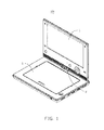
- FIG. 1 is an isometric view of an electronic device having a pivot mechanism and a sub-circuit board in accordance with an embodiment.
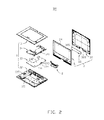
- FIG. 2 is an exploded of an electronic device in FIG. 1 .
- FIG. 3 is an isometric view of the pivot mechanism in FIG. 2 .
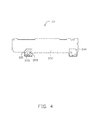
- FIG. 4 is an isometric view of the sub-circuit board in FIG. 2 .
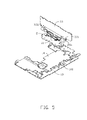
- FIG. 5 is an assembly view of a part of components of the electronic device in FIG. 2 .
- FIG. 1 is an electronic device 100 of an embodiment.
- the electronic device 100 includes a main body 1, a pivot mechanism 2, and a cover 3.
- the cover 3 is rotatably connected to the main body 1 to be opened from or folded down the main body 1.
- the electronic device 100 is a DVD player.
- FIG. 2 shows that the main body 1 includes an upper casing 11, a lower casing 12, a main circuit board 13, and a conductive sheet 14.
- the lower casing 12 is rectangular and includes a bottom side 121, and a side wall 122 extending from edges of the bottom side 121.
- the upper casing 11 covers the lower casing 12 to form a receiving space to receive the main circuit board 13, the conductive sheet 14, and other electronic elements.
- the main circuit board 13 is configured to control the main body 1 to perform corresponding functions.
- the main circuit board 13 includes a first conductive layer 131, and a first insulated layer 132.
- a first conductive portion 133 is arranged on an edge of the first conductive layer 131.
- the first conductive portion 133 is exposed out of the first insulated layer 132.
- a plurality of first through holes 134 are defined in the first conductive portion 133.
- the first though hole 134 runs through the main circuit board 13.
- the conductive sheet 14 is flat plate, made of conductive metal material, such as aluminum.
- the conductive sheet 14 defines a plurality of second through holes 141 corresponding to the second through holes 134. Securing members, such as screws (not shown), pass through the first through holes 141 and the second through holes 134 to secure the conductive sheet 14 to the main circuit board 13. As a result, the conductive sheet 14 is electrically connected to the first conductive portion 133, and the first conductive layer 131 is electrically connected to the conductive sheet 14.
- FIGs. 3 and 5 show that the pivot mechanism 2 is made of conductive metal and rigid material.
- the pivot mechanism 2 includes a bottom board 21, a securing part 22, a pivot shaft 23, two sleeves 24, a first wing board 25a, a second wing board 25b.
- Opposite ends (left and right ends) of the bottom board 21 respectively define two through holes 211.
- Conductive securing members, such as iron screws (not shown) pass through the through holes 211 defined in the right end of the bottom board 21 securing the bottom board 21 to the conductive sheet 14.
- conductive securing members (not shown) pass through the through holes 211 defined in the left end of the lower casing 12 securing the bottom board 21 to lower casing 12.
- the securing part 22 is a hollow cylinder perpendicularly protruding from one side of the bottom board 21 opposite to the conductive sheet 14.
- the pivot shaft 23 extends from one end of the securing part 22 away from the bottom board 21 in an opposite direction, parallel to the bottom board 21.
- the sleeves 24 are sleeved on opposite ends of the pivot shaft 23, and are rotated under external forces.
- the first wing board 25a and the second wing board 25b are secured on the sleeves 24.
- the first wing board 25a and the second wing board 25b define a plurality of third through holes 251.
- the cover 3 includes a front casing 31, a rear casing 32, and a sub-circuit board 33, a display panel 34, and other electronic components (not shown).
- the front casing 31 and the rear casing 32 are combined together to form a receiving space to receive the sub-circuit 33, the display panel 34, other electronic components, and a part of the pivot mechanism 2.
- the front casing 31 defines an opening (not labeled) in the middle enabling the display panel 34 to be exposed out of the front casing 31.
- the sub-circuit board 33 is configured to control the panel 34 to display information.
- FIGs. 4 and 5 show that sub-circuit board 33 includes a grounded second conductive layer 331, and a second insulated layer 332 covering the second conductive layer 331.
- the area of the second conductive layer 331 is smaller than the area of the first conductive layer 131.
- the second conductive layer 331 includes a second conductive part 333 and an insulated part 334.
- the second conductive part 333 and the insulated part 334 extend from one side of the sub-circuit board 33.
- the second conductive part 333 and the insulated part 334 are positioned at opposite ends of the sub-circuit board 33.
- the second conductive part 333 is exposed out of the second insulated layer 332 that covers the insulated part 334.
- the shapes of the second conductive part 333 and the insulated part 334 match the shapes of the first wing board 25a and the second wing board 25b.
- the second conductive part 333 and the insulated part 334 define a plurality of fourth through holes 335, the through holes 225 correspond to the third through holes 251.
- a plurality of securing members (not shown) pass through the third through holes 251 and the fourth through holes 335 securing the second conductive part 333 and the insulated part 334 to the first wing board 25a and the second wing board 25b.
- the second conductive part 33 is electrically connected to the first wing board 25a so that the second conductive part 33 is electrically connected to the pivot mechanism 2.
- the second insulated layer 331 covers the insulated part 334 so that the probability of electro-static discharge (ESD) flowing from the pivot mechanism 2 to the sub-circuit board 33 is diminished.
- the first conductive layer 131 of the main circuit board 13 is electrically connected to the pivot mechanism 2 via the conductive sheet 14 and the bottom board 21.
- the second conductive layer 331 of the sub-circuit bard 33 is electrically connected to the pivot mechanism 2 via the second conductive part 333 and the first wing board 25a.
- the second conductive layer 331 is electrically connected to the first conductive layer 131and the area of the second conductive layer 331 increases. Because the area of the second conductive layer 331 is smaller than that of the first conductive layer 131, when ESD occurs on the second conductive 331, an amount of the ESD will be transmitted to ground. The remainder of the ESD will be transmitted to the first conductive layer 131 and then transmitted to the ground via the pivot mechanism 2. As a result, the capacity of ESD protection for the sub-circuit board 33 is improved.
- the first conductive layer 131 of the main circuit board 131 is connected to the pivot mechanism by directly connecting the first conductive part 133 to the bottom board 21, and the conductive sheet 14 is omitted.
- the electronic device 100 using the pivot mechanism 2 to electrically connect the second conductive layer 331 to the first conductive layer to increase the area conduction, such that the capacity of ESD protection for the sub-circuit board is improved.
Landscapes
- Engineering & Computer Science (AREA)
- Theoretical Computer Science (AREA)
- Computer Hardware Design (AREA)
- Physics & Mathematics (AREA)
- General Engineering & Computer Science (AREA)
- General Physics & Mathematics (AREA)
- Human Computer Interaction (AREA)
- Power Engineering (AREA)
- Microelectronics & Electronic Packaging (AREA)
- Mounting Of Printed Circuit Boards And The Like (AREA)
- Switch Cases, Indication, And Locking (AREA)
- Telephone Set Structure (AREA)
- Casings For Electric Apparatus (AREA)
- Shielding Devices Or Components To Electric Or Magnetic Fields (AREA)
- Combinations Of Printed Boards (AREA)
Abstract
Description
- Electronic devices, such as portable DVD players include a main body, a display panel, and a metal pivot. The display panel is rotatably connected to the main body via the metal pivot. As display panels become miniaturized the circuit boards received in the display panel must be reduced in size as well. As a result, the electrical grounding area becomes smaller, reducing the capacity of the electro static discharge (ESD) protection for the circuit board.
- Therefore, there is room for improvement in the art.
- According to an exemplary embodiment of the invention, an electronic device includes a main body, a cover, a pivot mechanism, a main circuit board received in the main body, and a sub-circuit board received in the cover. The pivot mechanism is conductive, the main circuit board comprises a grounded first conductive layer, the sub-circuit board includes a grounded second conductive layer, the first conductive layer is connected to the second conductive layer. As a result, the pivot mechanism electrically connects the second conductive layer to the first conductive layer to increase the area conduction, such that the capacity of ESD protection for the sub-circuit board is improved.
- The components of the drawings are not necessarily drawn to scale, the emphasis instead being placed upon clearly illustrating the principles of the embodiments of an electronic device. Moreover, in the drawings, like reference numerals designate corresponding parts throughout one view.
-
FIG. 1 is an isometric view of an electronic device having a pivot mechanism and a sub-circuit board in accordance with an embodiment. -
FIG. 2 is an exploded of an electronic device inFIG. 1 . -
FIG. 3 is an isometric view of the pivot mechanism inFIG. 2 . -
FIG. 4 is an isometric view of the sub-circuit board inFIG. 2 . -
FIG. 5 is an assembly view of a part of components of the electronic device inFIG. 2 . -
FIG. 1 is anelectronic device 100 of an embodiment. Theelectronic device 100 includes amain body 1, apivot mechanism 2, and acover 3. Thecover 3 is rotatably connected to themain body 1 to be opened from or folded down themain body 1. In this embodiment, theelectronic device 100 is a DVD player. -
FIG. 2 shows that themain body 1 includes anupper casing 11, alower casing 12, amain circuit board 13, and aconductive sheet 14. Thelower casing 12 is rectangular and includes abottom side 121, and aside wall 122 extending from edges of thebottom side 121. Theupper casing 11 covers thelower casing 12 to form a receiving space to receive themain circuit board 13, theconductive sheet 14, and other electronic elements. - The
main circuit board 13 is configured to control themain body 1 to perform corresponding functions. Themain circuit board 13 includes a firstconductive layer 131, and a first insulatedlayer 132. A firstconductive portion 133 is arranged on an edge of the firstconductive layer 131. The firstconductive portion 133 is exposed out of the first insulatedlayer 132. A plurality of first throughholes 134 are defined in the firstconductive portion 133. The first thoughhole 134 runs through themain circuit board 13. - The
conductive sheet 14 is flat plate, made of conductive metal material, such as aluminum. Theconductive sheet 14 defines a plurality of second throughholes 141 corresponding to the second throughholes 134. Securing members, such as screws (not shown), pass through the first throughholes 141 and the second throughholes 134 to secure theconductive sheet 14 to themain circuit board 13. As a result, theconductive sheet 14 is electrically connected to the firstconductive portion 133, and the firstconductive layer 131 is electrically connected to theconductive sheet 14. -
FIGs. 3 and5 show that thepivot mechanism 2 is made of conductive metal and rigid material. Thepivot mechanism 2 includes abottom board 21, a securingpart 22, apivot shaft 23, twosleeves 24, a first wing board 25a, a second wing board 25b. Opposite ends (left and right ends) of thebottom board 21 respectively define two throughholes 211. Conductive securing members, such as iron screws (not shown) pass through the throughholes 211 defined in the right end of thebottom board 21 securing thebottom board 21 to theconductive sheet 14. In addition, conductive securing members (not shown) pass through the throughholes 211 defined in the left end of thelower casing 12 securing thebottom board 21 to lowercasing 12. Thesecuring part 22 is a hollow cylinder perpendicularly protruding from one side of thebottom board 21 opposite to theconductive sheet 14. Thepivot shaft 23 extends from one end of thesecuring part 22 away from thebottom board 21 in an opposite direction, parallel to thebottom board 21. Thesleeves 24 are sleeved on opposite ends of thepivot shaft 23, and are rotated under external forces. The first wing board 25a and the second wing board 25b are secured on thesleeves 24. The first wing board 25a and the second wing board 25b define a plurality of third throughholes 251. - The
cover 3 includes afront casing 31, arear casing 32, and asub-circuit board 33, adisplay panel 34, and other electronic components (not shown). Thefront casing 31 and therear casing 32 are combined together to form a receiving space to receive thesub-circuit 33, thedisplay panel 34, other electronic components, and a part of thepivot mechanism 2. Thefront casing 31 defines an opening (not labeled) in the middle enabling thedisplay panel 34 to be exposed out of thefront casing 31. Thesub-circuit board 33 is configured to control thepanel 34 to display information. -
FIGs. 4 and5 show thatsub-circuit board 33 includes a grounded secondconductive layer 331, and a second insulatedlayer 332 covering the secondconductive layer 331. The area of the secondconductive layer 331 is smaller than the area of the firstconductive layer 131. The secondconductive layer 331 includes a secondconductive part 333 and aninsulated part 334. The secondconductive part 333 and theinsulated part 334 extend from one side of thesub-circuit board 33. The secondconductive part 333 and theinsulated part 334 are positioned at opposite ends of thesub-circuit board 33. The secondconductive part 333 is exposed out of the secondinsulated layer 332 that covers theinsulated part 334. The shapes of the secondconductive part 333 and theinsulated part 334 match the shapes of the first wing board 25a and the second wing board 25b. The secondconductive part 333 and theinsulated part 334 define a plurality of fourth throughholes 335, the through holes 225 correspond to the third throughholes 251. A plurality of securing members (not shown) pass through the third throughholes 251 and the fourth throughholes 335 securing the secondconductive part 333 and theinsulated part 334 to the first wing board 25a and the second wing board 25b. As a result, the secondconductive part 33 is electrically connected to the first wing board 25a so that the secondconductive part 33 is electrically connected to thepivot mechanism 2. The second insulatedlayer 331 covers theinsulated part 334 so that the probability of electro-static discharge (ESD) flowing from thepivot mechanism 2 to thesub-circuit board 33 is diminished. - In the above-described
electronic device 100, the firstconductive layer 131 of themain circuit board 13 is electrically connected to thepivot mechanism 2 via theconductive sheet 14 and thebottom board 21. The secondconductive layer 331 of thesub-circuit bard 33 is electrically connected to thepivot mechanism 2 via the secondconductive part 333 and the first wing board 25a. As a result, the secondconductive layer 331 is electrically connected to the first conductive layer 131and the area of the secondconductive layer 331 increases. Because the area of the secondconductive layer 331 is smaller than that of the firstconductive layer 131, when ESD occurs on the second conductive 331, an amount of the ESD will be transmitted to ground. The remainder of the ESD will be transmitted to the firstconductive layer 131 and then transmitted to the ground via thepivot mechanism 2. As a result, the capacity of ESD protection for thesub-circuit board 33 is improved. - In another embodiment, the first
conductive layer 131 of themain circuit board 131 is connected to the pivot mechanism by directly connecting the firstconductive part 133 to thebottom board 21, and theconductive sheet 14 is omitted. - Furthermore, in order to improve the capacity of ESD protection, electronic components of the
sub-circuit board 33, such as ICs, diodes, and audio cards, which are easily damaged by ESD, are secured to positions ofsub-circuit board 33 away from the secondconductive part 333. As a result, a path for transmitting the ESD from the joint of thepivot mechanism 2 and the secondconductive part 333 to these electronic components is maximized, and the disruption of the ESD decreases. - As described above, the
electronic device 100 using thepivot mechanism 2 to electrically connect the secondconductive layer 331 to the first conductive layer to increase the area conduction, such that the capacity of ESD protection for the sub-circuit board is improved. - Further alternative embodiments will become apparent to those skilled in the art without departing from the spirit and scope of what is claimed. Accordingly, the present invention should be deemed not to be limited to the above detailed description, but rather only by the claims that follow and equivalents thereof.
Claims (10)
- An electronic device, comprising:a main body;a cover;a pivot mechanism;a main circuit board received in the main body; anda sub-circuit board received in the cover;wherein the pivot mechanism is conductive, the main circuit board comprises a first grounded conductive layer, the sub-circuit board comprises a second grounded conductive layer, the first conductive layer is electrically connected to the second conductive layer via the pivot mechanism.
- The electronic device of claim 1, wherein the area of the first conductive layer is larger than the area of the second conductive layer.
- The electronic device of claim 1 or 2, wherein the first conductive layer comprises a first conductive part electrically connected to the pivot mechanism, the main circuit board comprises a first insulated layer covered on the first conductive layer, the first conductive part is exposed out of the first insulated layer.
- The electronic device of claim 3, wherein the pivot mechanism comprises a bottom board, the bottom board is secured to the first conductive part so as to electrically connect to the first conductive layer.
- The electronic device of claim 1, 2, 3 or 4, wherein the second conductive layer comprises a second conductive part electrically connected to the pivot mechanism, the sub-circuit board comprises a second insulated layer covered on the second conductive layer, the second conductive part is exposed out of the second insulated layer.
- The electronic device of claim 5, wherein the pivot mechanism further comprises a first wing board, the first wing board is secured to the second conductive part so as to electrically connect to the second conductive layer.
- The electronic device of claim 6, wherein the shape of the second conductive part matches the shape of the first wing board.
- The electronic device of claim 5, 6 or 7, wherein the second conductive layer further comprises an insulated part covered by the second insulated layer, the pivot mechanism further comprises a second wing board, the insulated part is secured to the second wing board.
- The electronic device of claim 8, wherein the shape of the insulated part matches the shape of the second wing board.
- The electronic device of any preceding claim, wherein the pivot mechanism rotatably connects the cover to the main body.
Applications Claiming Priority (1)
| Application Number | Priority Date | Filing Date | Title |
|---|---|---|---|
| CN2012101706997A CN103458635A (en) | 2012-05-29 | 2012-05-29 | Electronic device |
Publications (2)
| Publication Number | Publication Date |
|---|---|
| EP2677389A2 true EP2677389A2 (en) | 2013-12-25 |
| EP2677389A3 EP2677389A3 (en) | 2014-07-23 |
Family
ID=48746205
Family Applications (1)
| Application Number | Title | Priority Date | Filing Date |
|---|---|---|---|
| EP13168388.0A Withdrawn EP2677389A3 (en) | 2012-05-29 | 2013-05-17 | Electronic device |
Country Status (5)
| Country | Link |
|---|---|
| US (1) | US20130322005A1 (en) |
| EP (1) | EP2677389A3 (en) |
| JP (1) | JP2013247368A (en) |
| CN (1) | CN103458635A (en) |
| TW (1) | TW201349230A (en) |
Families Citing this family (4)
| Publication number | Priority date | Publication date | Assignee | Title |
|---|---|---|---|---|
| TWI594666B (en) * | 2015-08-10 | 2017-08-01 | 緯創資通股份有限公司 | Electro-static discharge protection structure and electronic device |
| CN110213953A (en) * | 2016-06-20 | 2019-09-06 | 海信集团有限公司 | Laser cinema equipment |
| WO2018094890A1 (en) * | 2016-11-28 | 2018-05-31 | 华为技术有限公司 | Notebook computer |
| CN116708626A (en) * | 2023-07-25 | 2023-09-05 | 维沃移动通信有限公司 | folding terminal |
Family Cites Families (10)
| Publication number | Priority date | Publication date | Assignee | Title |
|---|---|---|---|---|
| US5608604A (en) * | 1994-09-22 | 1997-03-04 | Apple Computer, Inc. | Hinge as an electrical conductor |
| JPH09153931A (en) * | 1995-11-30 | 1997-06-10 | Mitsubishi Electric Corp | Opening and closing mechanism |
| US6347035B1 (en) * | 1998-10-30 | 2002-02-12 | Fujitsu Limited | Low profile EMI shield with heat spreading plate |
| US6249426B1 (en) * | 1999-08-30 | 2001-06-19 | Dell Usa Corp | Portable computer having a sealed hinge clutch |
| US6266238B1 (en) * | 2000-02-28 | 2001-07-24 | Dell Usa, L.P. | Electromagnetic emission shielding apparatus |
| JP4319507B2 (en) * | 2003-10-07 | 2009-08-26 | 京セラ株式会社 | Portable electronic devices |
| JP4312072B2 (en) * | 2004-02-17 | 2009-08-12 | パナソニック株式会社 | Portable radio |
| JP4563943B2 (en) * | 2006-01-30 | 2010-10-20 | 京セラ株式会社 | Mobile phone |
| KR20080054651A (en) * | 2006-12-13 | 2008-06-19 | 삼성전자주식회사 | Portable terminal with variable grounding device |
| JP5040532B2 (en) * | 2007-08-31 | 2012-10-03 | 富士通株式会社 | Electronics |
-
2012
- 2012-05-29 CN CN2012101706997A patent/CN103458635A/en active Pending
- 2012-05-31 TW TW101119495A patent/TW201349230A/en unknown
-
2013
- 2013-04-15 US US13/862,521 patent/US20130322005A1/en not_active Abandoned
- 2013-05-17 EP EP13168388.0A patent/EP2677389A3/en not_active Withdrawn
- 2013-05-27 JP JP2013110714A patent/JP2013247368A/en active Pending
Also Published As
| Publication number | Publication date |
|---|---|
| CN103458635A (en) | 2013-12-18 |
| JP2013247368A (en) | 2013-12-09 |
| EP2677389A3 (en) | 2014-07-23 |
| US20130322005A1 (en) | 2013-12-05 |
| TW201349230A (en) | 2013-12-01 |
Similar Documents
| Publication | Publication Date | Title |
|---|---|---|
| KR102944448B1 (en) | Foldable electronic device including display protection structure | |
| RU2768781C1 (en) | Folding electronic device comprising an integrated grounding structure | |
| EP3771186A1 (en) | Electronic device including foldable conductive plate | |
| US9332329B2 (en) | Electronic apparatus | |
| JP6535353B2 (en) | Portable information equipment | |
| EP4629442A2 (en) | Antenna having single non-conductive portion and electronic device including the same | |
| CN104599593B (en) | display device | |
| US9137918B2 (en) | Electronic apparatus and method for assembling the same | |
| EP3683650B1 (en) | Display screen assembly and mobile terminal | |
| US20150169005A1 (en) | Electronic device and touchpad assembly | |
| EP3448056B1 (en) | Electronic device including electronic part and earphone jack assembly | |
| CN113748395A (en) | Electronic device including dual display | |
| US20130322005A1 (en) | Electronic device | |
| JP6491770B2 (en) | Portable information equipment | |
| US9282668B2 (en) | Electronic apparatus and method for assembling the same | |
| CN104582384A (en) | Electronic assembly and electronic device | |
| US8243440B2 (en) | Foldable computing device with counterbalance member | |
| JP4282671B2 (en) | Electronics | |
| JP2008083982A (en) | Electronics | |
| WO2011061858A1 (en) | Display device and electronic apparatus | |
| US8536461B2 (en) | Printed circuit board having stiff and flexible characteristics | |
| GB2591840A (en) | Electronic devices comprising printed circuit boards | |
| US9442582B2 (en) | Portable electronic device with a surface mounted technology touch pad | |
| JP5148078B2 (en) | Circuit module and electronic device | |
| US20130335930A1 (en) | Electronic apparatus |
Legal Events
| Date | Code | Title | Description |
|---|---|---|---|
| PUAI | Public reference made under article 153(3) epc to a published international application that has entered the european phase |
Free format text: ORIGINAL CODE: 0009012 |
|
| AK | Designated contracting states |
Kind code of ref document: A2 Designated state(s): AL AT BE BG CH CY CZ DE DK EE ES FI FR GB GR HR HU IE IS IT LI LT LU LV MC MK MT NL NO PL PT RO RS SE SI SK SM TR |
|
| AX | Request for extension of the european patent |
Extension state: BA ME |
|
| PUAL | Search report despatched |
Free format text: ORIGINAL CODE: 0009013 |
|
| AK | Designated contracting states |
Kind code of ref document: A3 Designated state(s): AL AT BE BG CH CY CZ DE DK EE ES FI FR GB GR HR HU IE IS IT LI LT LU LV MC MK MT NL NO PL PT RO RS SE SI SK SM TR |
|
| AX | Request for extension of the european patent |
Extension state: BA ME |
|
| RIC1 | Information provided on ipc code assigned before grant |
Ipc: G06F 1/16 20060101AFI20140616BHEP Ipc: G06F 1/18 20060101ALI20140616BHEP |
|
| STAA | Information on the status of an ep patent application or granted ep patent |
Free format text: STATUS: THE APPLICATION IS DEEMED TO BE WITHDRAWN |
|
| 18D | Application deemed to be withdrawn |
Effective date: 20150124 |