EP2677375A2 - Apparatus and method for controlling input signal - Google Patents
Apparatus and method for controlling input signal Download PDFInfo
- Publication number
- EP2677375A2 EP2677375A2 EP13165934.4A EP13165934A EP2677375A2 EP 2677375 A2 EP2677375 A2 EP 2677375A2 EP 13165934 A EP13165934 A EP 13165934A EP 2677375 A2 EP2677375 A2 EP 2677375A2
- Authority
- EP
- European Patent Office
- Prior art keywords
- input signal
- plc
- error
- signal
- estimation parameter
- Prior art date
- Legal status (The legal status is an assumption and is not a legal conclusion. Google has not performed a legal analysis and makes no representation as to the accuracy of the status listed.)
- Granted
Links
Images




Classifications
-
- G—PHYSICS
- G05—CONTROLLING; REGULATING
- G05B—CONTROL OR REGULATING SYSTEMS IN GENERAL; FUNCTIONAL ELEMENTS OF SUCH SYSTEMS; MONITORING OR TESTING ARRANGEMENTS FOR SUCH SYSTEMS OR ELEMENTS
- G05B19/00—Program-control systems
- G05B19/02—Program-control systems electric
- G05B19/04—Program control other than numerical control, i.e. in sequence controllers or logic controllers
- G05B19/05—Programmable logic controllers, e.g. simulating logic interconnections of signals according to ladder diagrams or function charts
- G05B19/054—Input/output
-
- G—PHYSICS
- G05—CONTROLLING; REGULATING
- G05B—CONTROL OR REGULATING SYSTEMS IN GENERAL; FUNCTIONAL ELEMENTS OF SUCH SYSTEMS; MONITORING OR TESTING ARRANGEMENTS FOR SUCH SYSTEMS OR ELEMENTS
- G05B15/00—Systems controlled by a computer
- G05B15/02—Systems controlled by a computer electric
-
- G—PHYSICS
- G05—CONTROLLING; REGULATING
- G05B—CONTROL OR REGULATING SYSTEMS IN GENERAL; FUNCTIONAL ELEMENTS OF SUCH SYSTEMS; MONITORING OR TESTING ARRANGEMENTS FOR SUCH SYSTEMS OR ELEMENTS
- G05B19/00—Program-control systems
- G05B19/02—Program-control systems electric
- G05B19/04—Program control other than numerical control, i.e. in sequence controllers or logic controllers
- G05B19/042—Program control other than numerical control, i.e. in sequence controllers or logic controllers using digital processors
- G05B19/0423—Input/output
Definitions
- the embodiment relates to an apparatus and a method for controlling an input signal, which can exactly measure a signal input to a PLC (Programmable Logic Controller).
- PLC Programmable Logic Controller
- Automatic equipment used in industrial fields consists of mechanical equipment including a relay. There is a difficulty to change the automatic equipment consisting of the mechanical equipment because internal circuits of the automatic equipment must be changed. In order to overcome such a difficulty, the PLC is used.
- the PLC includes an analog input module.
- the analog input module of the PLC may include a circuit for converting an analog input signal into a digital value.
- the analog input signal may include an analog direct current or an analog direct current voltage.
- the analog input module of the PLC may measure a value of the analog input signal after receiving the analog input signal.
- hardware such as a resistor or an amplifier (OP-Amp) which constitutes the analog input module, causes an error in an analog input signal value, it is difficult to exactly measure the analog input signal value.
- the analog input signal may be corrected based on the reference signal in order to exactly measure the analog input signal value.
- the signal correcting scheme using a linear equation according to the related art measures the analog input signal several times, this scheme requires much time and, when the analog input signal is a nonlinear signal, this scheme cannot be applied.
- the embodiment provides an apparatus and a method for controlling an input signal capable of improving the performance of an analog input module by correcting an error of a signal received in the analog input module.
- the embodiment provides an apparatus and a method for adaptively controlling a signal capable of correcting an error of a signal received in an analog input module according to a variation of PLC ambient environment.
- an apparatus for controlling a signal such that a PLC input signal is equalized to a reference input signal includes an error calculation unit to calculate an error by using the PLC input signal and the reference input signal; an estimation parameter calculation unit to calculate an estimation parameter by using the reference input signal, the PLC input signal and the error; and an error correction unit to correct the error by using the estimation parameter such that the PLC input signal is equalized to the reference input signal.
- a method of controlling a signal such that a PLC input signal is equalized to a reference input signal includes generating a PLC output signal by applying a first transfer function to the PLC input signal; generating a reference output signal by applying a second transfer function to the reference input signal; calculating an error of the PLC input signal by using the PLC output signal and the reference output signal; calculating an estimation parameter by using the reference input signal, the PLC output signal and the error; and correcting the error by using the estimation parameter such that the PLC input signal is equalized to the reference input signal.
- the performance of the analog input module can be improved by correcting the error of the signal received in the analog input module.
- the error of the signal received in the analog input module can be adaptively corrected according to a variation of PLC ambient environment.
- FIG. 1 is a block diagram showing an apparatus for providing an image according to the embodiment
- FIG. 2 is a view substantially showing an apparatus for controlling a PLC analog input signal in continuous time domain according to the embodiment
- FIG. 3 is a substantial view showing a PLC analog input signal controlling apparatus in time division domain according to the embodiment
- FIG. 4 is a view showing an estimation parameter on a graph, which is determined by a method of controlling a signal according to the embodiment.
- FIG. 5 is a view showing, on a graph, a result of approximating a PLC analog input signal to a reference value according to a method of controlling a signal of the embodiment.
- a predetermined part when referred as to "include” a predetermined component, the predetermined part does not exclude other components, but may further include other components unless indicated otherwise.
- FIG. 1 is a block diagram showing an apparatus for providing an image according to the embodiment.
- an analog input module includes an input channel, a noise reducing unit, a filter and an amplifier.
- the input channel may include a plus terminal CH+ and a minus terminal CH- and an input voltage Vin may be input to the plus and minus terminals CH+ and CH-.
- the noise reducing unit includes a plurality of capacitors C1, C2 and C3.
- One terminal of the first capacitor C1 may be connected to the plus terminal CH+ of the input channel and the other terminal of the first capacitor C1 may be grounded.
- One terminal of the second capacitor C2 may be connected to the minus terminal CH- of the input channel and the other terminal of the second capacitor C2 may be grounded.
- One terminal of the third capacitor C3 may be connected to the plus terminal CH+ of the input channel and the other terminal of the third capacitor C3 may be connected to the one terminal of the second capacitor C2 connected to the minus channel CH- of the input channel.
- the noise reducing unit including the plurality of capacitors may be remove a noise from an analog input signal received through the input channel.
- the filter includes a plurality of resistors R1 and R2 and a plurality of capacitors C4 and C5.
- the filter including the resistors and the capacitors which is called an RC filter, allows a specific frequency signal of the input signal to pass therethrough or to be blocked, so that the filter allows the input signal to selectively pass therethrough.
- One terminal of the first resistor R1 may be connected to the one terminal of the third capacitor C3 of the noise reducing unit and one terminal of the second resistor R2 may be connected to the other terminal of the third capacitor C3 of the noise reducing unit.
- the other terminal of the first resistor R1 may be connected to one terminal of the fourth capacitor C4, and the other terminal of the second resistor R2 may be connected to one terminal of the fifth capacitor C5.
- a first voltage V1 applied to the fourth and fifth capacitors C4 and C5 may be considered as the input signal measured at the analog input module when taking into account the features of an RC filter.
- the first voltage V1 is a signal which is output from the filter according to a predetermined transfer function after the signal has been input to the PLC analog input module and a noise of the input signal has been removed.
- a transfer function T(s) in Laplace domain which is a continuously time domain may be expressed as following Equation 1:
- Equation 1 R is the first or second resistor R1 or R2, C is the fourth or fifth capacitor C4 or C5.
- the transfer function may be expressed as a time division domain transfer function of following Equation 2:
- T z 0.6768 ⁇ z + 0.6768 z + 0.4027
- Equation 2 is obtained by z-transforming Equation 1 which is a Laplace transfer function.
- the amplifier may include a plurality of Op-AMPs and a plurality of resistors.
- An amplifier having an amplifier gain required for the function of the PLC analog input module may be used.
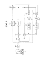
- FIG. 2 is a view substantially showing an apparatus for controlling a PLC analog input signal in continuous time domain according to the embodiment.
- the PLC analog input signal controlling apparatus 200 includes a first operation unit 201, a second operation unit 203, an error calculation unit, a first parameter operation unit, a second parameter operation unit, an error correction unit.
- the first operation unit 201 applies a first transfer function H 1 (s) to an analog input signal u, thereby generating an analog output signal y.
- the analog input signal u and the analog output signal y signify signals before correction.
- the gain of the first transfer function H 1 (s) may include not '1' but a constant such as the transfer function T(s) of Equation 1.
- the analog output signal y is denoted as a first-order differential equation in time domain, the analog output signal y is expressed as following Equation 3:
- dy dt - 1 RC ⁇ y + Gain RC ⁇ u
- R denotes a resistor constituting the filter included in the first operation unit 201
- C denotes a capacitor constituting the filter included in the first operation unit 201.
- the second operation unit 203 generates a reference output signal y m by applying a second transfer function H 2 (s) to the reference input signal u c .
- the reference input signal u c is input to the analog input signal controlling apparatus 200 in order to correct the analog input signal u. That is, the reference input signal u c and the reference output signal y m signify reference signals for correcting the analog input signal u and the analog output signal y, that are, signals after correction.
- the second transfer function H 2 (s) has the same degree and coefficient as those of the first transfer function H 1 (s). Only, the gain of the transfer function H 2 (s) is '1' and in this regard, the second transfer function H 2 (s) is different from the first transfer function H 1 (s). If the second transfer function H 2 (s) is expressed corresponding to Equation 1, the second transfer function H 2 (s) may be expressed as following Equation 4:
- the reference output signal y m may be expressed in a form of a first-order differential equation in time domain as following Equation 5:
- the error calculation unit generates an error signal e by calculating a difference between the analog output signal y generated from the first operation unit 201 and the reference output signal y m generated from the second operation unit 203.
- the error calculation unit may include a first sigma unit 205.
- the error signal e may be expressed as following Equation 6:
- Equation 6 is an equation derived for estimating a parameter for correcting the analog input signal u. That is, a parameter, which allows the analog input signal u to approximate to the reference input signal u c by using the error signal e, may be evaluated.
- the first parameter operation unit includes a first multiplier 207, a first amplifier 211 and a first integrator 215.
- the first multiplier 207 multiplies the reference signal u c and the error signal e generated from the error calculation unit to generate a multiplication result.
- the first amplifier 211 amplifies the multiplication result generated from the first multiplier 207 at the first gain G 1 to generate an amplification result.
- the first integrator 215 integrates the amplification result generated from the first amplifier 211 to generate an integration result.
- the operations of the first multiplier 207, the first amplifier 211 and the first integrator 215 may be sequentially performed, but the embodiment is not limited thereto.
- Equation 7 is for estimating a first parameter ⁇ 1 based on the error signal e, the reference input signal u c and the first gain G 1 .
- the first parameter operation unit may evaluates the first parameter ⁇ 1 expressed as Equation 7 by using the first multiplier 207, the first amplifier 211 and the first integrator 215.
- the second parameter operation unit includes a second multiplier 209, a second amplifier 213 and a second integrator 217.
- the second multiplier 209 multiplies the analog output y generated for the first operation unit 201 and the error signal e generated from the error calculation unit to generate a multiplication result.
- the second amplifier 213 amplifies the multiplication result generated from the second multiplier 209 at the second gain G 2 to generate an amplification result.
- the second integrator 217 integrates the amplification result generated from the second amplifier 213 to generate an integration result.
- the operations of the second multiplier 209, the second amplifier 213 and the second integrator 217 may be sequentially performed, but the embodiment is not limited thereto.
- Equation 8 is for estimating a second parameter ⁇ 2 based on the error signal e, the reference input signal u c and the second gain G 2 .
- the second parameter operation unit may evaluates the second parameter ⁇ 2 expressed as Equation 8 by using the second multiplier 209, the second amplifier 213 and the second integrator 217.
- Equations 7 and 8 are calculated by using following Equation 10 derived from Equations 3, 5 and 6 and following Equation 9.
- Equation 9 is derived in terms of the analog input signal u in order to estimating the first and second parameters ⁇ 1 and ⁇ 2 .
- the input signal after correction may be evaluated by using Equation 9 as .
- the analog signal u is corrected by using the results of applying the first parameter ⁇ 1 to the reference input signal u c and applying the second parameter ⁇ 2 to the analog output signal y.
- the control of correcting an input according to an output may be called an adaptive control.
- An error of a signal received in the analog input module may be corrected according to a variation of PLC ambient environment, for example, a variation of ambient temperature, and an error of an nonlinear input signal may be also corrected through the adaptive control.
- Equation 10 may be derived by using Equations 3, 5, 6 and 9:
- Equation 11 An estimation equation, which is derived by integrating Equation 10 and has the error signal e, and the first and second parameters ⁇ 1 and ⁇ 2 as dependent variables, may be expressed as following Equation 11:
- V e ⁇ ⁇ 1 ⁇ ⁇ 2 1 2 ⁇ e 2 + 1 G 2 ⁇ RC Gain ⁇ Gain RC ⁇ ⁇ 2 + 1 RC - a m 2 + 1 G 1 ⁇ RC Gain ⁇ Gain RC ⁇ ⁇ 1 - b m 2
- Equation 12 is a differential equation which results from differentiating the estimation equation of Equation 11 with respect to time t.
- Equation 12 is an equation in terms of the first and second parameters ⁇ 1 and ⁇ 2 , which is derived from the estimation differential equation.
- the error signal e of Equation 6 must be convergent to 0.
- a differential value (de/dt) of the error signal of Equation 10 must be less than 0.
- the estimation equation V(e, ⁇ 1 , ⁇ 2 ) of Equation 11 must be greater than 0.
- a differential value (dv/dt) of the estimation equation of Equation 12 must be less than 0.
- the error correction unit performs the calculation such as Equation 9.
- the error correction unit may include a third multiplier 219, a fourth multiplier 221 and a second sigma unit 223.
- the third multiplier 219 may generate a result of applying the first parameter ⁇ 1 to the reference input signal u c .
- the fourth multiplier 221 may generate a result of applying the second parameter ⁇ 2 to the analog output signal y.
- the second sigma unit 223 may generate a difference value between the results generated from the third multiplier 219 and generated from the fourth multiplier 221.
- the difference value between the results generated from the third multiplier 219 and generated from the fourth multiplier 221 signifies the analog input signal u.
- a next analog input signal u is generated by using the reference input signal u c and the value output from the system such as the first operation unit 201 to which a previous analog input signal u is input.
- FIG. 3 is a substantial view showing a PLC analog input signal controlling apparatus in time division domain according to the embodiment.
- the PLC analog input signal controlling apparatus includes a first operation unit 301, a second operation unit 303, an error calculation unit, a first parameter operation unit, a second parameter operation unit, and an error correction unit.
- FIG. 3 is a view showing the PLC analog input signal controlling apparatus of continuous time domain of FIG. 2 in time division domain. Although the configuration of FIG. 3 is almost similar to that of FIG. 2 , there are differences in calculations of the transfer function and the integrator between FIGS. 2 and 3 . Thus, the following descriptions will be made while focusing on the difference with respect to FIG. 2 and the same description will be omitted.
- the first operation unit 301 generates the analog output signal y by applying the first transfer function H 1 (z) to the analog input signal u.
- the first transfer function H 1 (z) may be expressed as following Equation 13:
- the second operation unit 303 generates the reference output signal y m by applying the second transfer function H 2 (z) to the reference input signal u c .
- the second transfer function H 2 (z) may be expressed as following Equation 14:
- the error calculation unit calculates the difference between the analog output signal y generated from the first operation unit 301 and the reference output signal y m generated from the second operation unit 303 to generate an error signal e.
- the first parameter operation unit includes a first multiplier 307, a first amplifier 311 and a first integrator 315.
- the first integrator 315 integrates the results generated from the first amplifier 311. There is a difference between the integrator for time division domain of FIG. 3 and integrator for continuous time domain of FIG. 2 . The difference may be caused because the integrator is z-converted in order to apply the PLC analog input signal controlling apparatus into digital domain.
- the PLC analog input signal controlling apparatus further includes a zero order hold 325.
- a sampling period for using the zero order hold 325 is set into 0.001 second.
- FIG. 4 is a view showing an estimation parameter on a graph, which is determined by a method of controlling a signal according to the embodiment.
- the first and second parameters ⁇ 1 and ⁇ 12 expressed in Equations 7 and 8 approximate gradually to final values through an adaptive control.
- the first and second parameters ⁇ 1 and ⁇ 12 are convergent to the final values.
- FIG. 5 is a view showing, on a graph, a result of approximating a PLC analog input signal to a reference value according to a method of controlling a signal of the embodiment.
- the real model output y is generated in a scheme of gradually tracking a value of the reference signal for correction.
- an amplitude of the reference signal r for correction may be in the permission range of the PLC analog input module and the reference signal r for correction may include a non-linear property.
- the embodiment described above can be implemented not only through an apparatus and a method, but also through a program which executes the functions corresponding to the elements of the embodiment or recording media on which the program is recorded. Such an implementation may be readily embodied by those skilled in the art based on the above disclosure.
Landscapes
- Engineering & Computer Science (AREA)
- Physics & Mathematics (AREA)
- General Physics & Mathematics (AREA)
- Automation & Control Theory (AREA)
- General Engineering & Computer Science (AREA)
- Programmable Controllers (AREA)
- Analogue/Digital Conversion (AREA)
Abstract
Description
- The embodiment relates to an apparatus and a method for controlling an input signal, which can exactly measure a signal input to a PLC (Programmable Logic Controller).
- Automatic equipment used in industrial fields consists of mechanical equipment including a relay. There is a difficulty to change the automatic equipment consisting of the mechanical equipment because internal circuits of the automatic equipment must be changed. In order to overcome such a difficulty, the PLC is used.
- The PLC includes an analog input module. The analog input module of the PLC may include a circuit for converting an analog input signal into a digital value. The analog input signal may include an analog direct current or an analog direct current voltage.
- In order to convert an analog input signal into a digital signal, the analog input module of the PLC may measure a value of the analog input signal after receiving the analog input signal. However, since hardware, such as a resistor or an amplifier (OP-Amp) which constitutes the analog input module, causes an error in an analog input signal value, it is difficult to exactly measure the analog input signal value.
- Therefore, after a reference signal is input to the analog input module, the analog input signal may be corrected based on the reference signal in order to exactly measure the analog input signal value. However, since the signal correcting scheme using a linear equation according to the related art measures the analog input signal several times, this scheme requires much time and, when the analog input signal is a nonlinear signal, this scheme cannot be applied.
- The embodiment provides an apparatus and a method for controlling an input signal capable of improving the performance of an analog input module by correcting an error of a signal received in the analog input module.
- Further, the embodiment provides an apparatus and a method for adaptively controlling a signal capable of correcting an error of a signal received in an analog input module according to a variation of PLC ambient environment.
- According to the embodiment, there is provided an apparatus for controlling a signal such that a PLC input signal is equalized to a reference input signal. The apparatus includes an error calculation unit to calculate an error by using the PLC input signal and the reference input signal; an estimation parameter calculation unit to calculate an estimation parameter by using the reference input signal, the PLC input signal and the error; and an error correction unit to correct the error by using the estimation parameter such that the PLC input signal is equalized to the reference input signal.
- According to the embodiment, there is provided a method of controlling a signal such that a PLC input signal is equalized to a reference input signal. The method includes generating a PLC output signal by applying a first transfer function to the PLC input signal; generating a reference output signal by applying a second transfer function to the reference input signal; calculating an error of the PLC input signal by using the PLC output signal and the reference output signal; calculating an estimation parameter by using the reference input signal, the PLC output signal and the error; and correcting the error by using the estimation parameter such that the PLC input signal is equalized to the reference input signal.
- According to the embodiment, the performance of the analog input module can be improved by correcting the error of the signal received in the analog input module.
- According to the embodiment, the error of the signal received in the analog input module can be adaptively corrected according to a variation of PLC ambient environment.
-
FIG. 1 is a block diagram showing an apparatus for providing an image according to the embodiment; -
FIG. 2 is a view substantially showing an apparatus for controlling a PLC analog input signal in continuous time domain according to the embodiment; -
FIG. 3 is a substantial view showing a PLC analog input signal controlling apparatus in time division domain according to the embodiment; -
FIG. 4 is a view showing an estimation parameter on a graph, which is determined by a method of controlling a signal according to the embodiment; and -
FIG. 5 is a view showing, on a graph, a result of approximating a PLC analog input signal to a reference value according to a method of controlling a signal of the embodiment. - Hereinafter, embodiments will be described in detail with reference to accompanying drawings so that those skilled in the art can easily work with the embodiments. However, the embodiments may not be limited to those described below, but have various modifications. The elements, which are not concerned with the description of the embodiments may be omitted in the drawings for the purpose of convenience or clarity. The same reference numbers will be assigned to the same elements throughout the drawings.
- In the following description, when a part is referred as to be connected to the other part, the parts are not only directly connected to each other, but also electrically connected to each other while interposing another part therebetween.
- In the following description, when a predetermined part is referred as to "include" a predetermined component, the predetermined part does not exclude other components, but may further include other components unless indicated otherwise.
-
FIG. 1 is a block diagram showing an apparatus for providing an image according to the embodiment. - Referring to
FIG. 1 , an analog input module includes an input channel, a noise reducing unit, a filter and an amplifier. - The input channel may include a plus terminal CH+ and a minus terminal CH- and an input voltage Vin may be input to the plus and minus terminals CH+ and CH-.
- The noise reducing unit includes a plurality of capacitors C1, C2 and C3. One terminal of the first capacitor C1 may be connected to the plus terminal CH+ of the input channel and the other terminal of the first capacitor C1 may be grounded. One terminal of the second capacitor C2 may be connected to the minus terminal CH- of the input channel and the other terminal of the second capacitor C2 may be grounded. One terminal of the third capacitor C3 may be connected to the plus terminal CH+ of the input channel and the other terminal of the third capacitor C3 may be connected to the one terminal of the second capacitor C2 connected to the minus channel CH- of the input channel. The noise reducing unit including the plurality of capacitors may be remove a noise from an analog input signal received through the input channel. Although it is assumed in the embodiment that the noise reducing unit includes only three capacitors, the embodiment is not limited thereto and it is not necessary to limit the configuration of the noise reducing unit to capacitors.
- The filter includes a plurality of resistors R1 and R2 and a plurality of capacitors C4 and C5. The filter including the resistors and the capacitors, which is called an RC filter, allows a specific frequency signal of the input signal to pass therethrough or to be blocked, so that the filter allows the input signal to selectively pass therethrough. One terminal of the first resistor R1 may be connected to the one terminal of the third capacitor C3 of the noise reducing unit and one terminal of the second resistor R2 may be connected to the other terminal of the third capacitor C3 of the noise reducing unit. The other terminal of the first resistor R1 may be connected to one terminal of the fourth capacitor C4, and the other terminal of the second resistor R2 may be connected to one terminal of the fifth capacitor C5. The other terminals of the fourth and fifth capacitors C4 and C5 may be grounded. A first voltage V1 applied to the fourth and fifth capacitors C4 and C5 may be considered as the input signal measured at the analog input module when taking into account the features of an RC filter. The first voltage V1 is a signal which is output from the filter according to a predetermined transfer function after the signal has been input to the PLC analog input module and a noise of the input signal has been removed. A transfer function T(s) in Laplace domain which is a continuously time domain may be expressed as following Equation 1:
-

- In
Equation 1, R is the first or second resistor R1 or R2, C is the fourth or fifth capacitor C4 or C5. In the case of C1=C2=0.01 µF, C3=0.47 µF, C4=C5=0.0047 µF, R1=R2=453 kΩ and R3=R4=49.9 kΩ, the transfer function having the coefficient and the gain ofEquation 1 may be calculated. - Further, the transfer function may be expressed as a time division domain transfer function of following Equation 2:
-

- In the case of the sampling period of 0.001 second,
Equation 2 is obtained by z-transformingEquation 1 which is a Laplace transfer function. - The amplifier may include a plurality of Op-AMPs and a plurality of resistors. An amplifier having an amplifier gain required for the function of the PLC analog input module may be used. The amplifier shown in
FIG. 1 is the amplifier of the model No. INA126U having a gain
-
FIG. 2 is a view substantially showing an apparatus for controlling a PLC analog input signal in continuous time domain according to the embodiment. - Referring to
FIG. 2 , the PLC analog inputsignal controlling apparatus 200 includes afirst operation unit 201, asecond operation unit 203, an error calculation unit, a first parameter operation unit, a second parameter operation unit, an error correction unit. - The
first operation unit 201 applies a first transfer function H1(s) to an analog input signal u, thereby generating an analog output signal y. the analog input signal u and the analog output signal y signify signals before correction. As thefirst operation unit 201 corresponds to the analog input module ofFIG. 1 , the gain of the first transfer function H1(s) may include not '1' but a constant such as the transfer function T(s) ofEquation 1. When the analog output signal y is denoted as a first-order differential equation in time domain, the analog output signal y is expressed as following Equation 3: -

where R denotes a resistor constituting the filter included in thefirst operation unit 201, and C denotes a capacitor constituting the filter included in thefirst operation unit 201. - The
second operation unit 203 generates a reference output signal ym by applying a second transfer function H2(s) to the reference input signal uc. The reference input signal uc is input to the analog inputsignal controlling apparatus 200 in order to correct the analog input signal u. That is, the reference input signal uc and the reference output signal ym signify reference signals for correcting the analog input signal u and the analog output signal y, that are, signals after correction. The second transfer function H2(s) has the same degree and coefficient as those of the first transfer function H1(s). Only, the gain of the transfer function H2(s) is '1' and in this regard, the second transfer function H2(s) is different from the first transfer function H1(s). If the second transfer function H2(s) is expressed corresponding toEquation 1, the second transfer function H2(s) may be expressed as following Equation 4: -

- The reference output signal ym may be expressed in a form of a first-order differential equation in time domain as following Equation 5:
-

wherein am and bm are parameters of the reference signal. - The error calculation unit generates an error signal e by calculating a difference between the analog output signal y generated from the
first operation unit 201 and the reference output signal ym generated from thesecond operation unit 203. The error calculation unit may include afirst sigma unit 205. The error signal e may be expressed as following Equation 6: -

- Equation 6 is an equation derived for estimating a parameter for correcting the analog input signal u. That is, a parameter, which allows the analog input signal u to approximate to the reference input signal uc by using the error signal e, may be evaluated.
- The first parameter operation unit includes a
first multiplier 207, afirst amplifier 211 and afirst integrator 215. - The
first multiplier 207 multiplies the reference signal uc and the error signal e generated from the error calculation unit to generate a multiplication result. - The
first amplifier 211 amplifies the multiplication result generated from thefirst multiplier 207 at the first gain G1 to generate an amplification result. - The
first integrator 215 integrates the amplification result generated from thefirst amplifier 211 to generate an integration result. - The operations of the
first multiplier 207, thefirst amplifier 211 and thefirst integrator 215 may be sequentially performed, but the embodiment is not limited thereto. - Following
Equation 7 is for estimating a first parameter θ1 based on the error signal e, the reference input signal uc and the first gain G1. -

- The first parameter operation unit may evaluates the first parameter θ1 expressed as
Equation 7 by using thefirst multiplier 207, thefirst amplifier 211 and thefirst integrator 215. - The second parameter operation unit includes a
second multiplier 209, asecond amplifier 213 and asecond integrator 217. - The
second multiplier 209 multiplies the analog output y generated for thefirst operation unit 201 and the error signal e generated from the error calculation unit to generate a multiplication result. - The
second amplifier 213 amplifies the multiplication result generated from thesecond multiplier 209 at the second gain G2 to generate an amplification result. - The
second integrator 217 integrates the amplification result generated from thesecond amplifier 213 to generate an integration result. - The operations of the
second multiplier 209, thesecond amplifier 213 and thesecond integrator 217 may be sequentially performed, but the embodiment is not limited thereto. - Following Equation 8 is for estimating a second parameter θ2 based on the error signal e, the reference input signal uc and the second gain G2.
-

- The second parameter operation unit may evaluates the second parameter θ2 expressed as Equation 8 by using the
second multiplier 209, thesecond amplifier 213 and thesecond integrator 217. -
Equations 7 and 8 are calculated by using followingEquation 10 derived fromEquations 3, 5 and 6 and following Equation 9. -

- Equation 9 is derived in terms of the analog input signal u in order to estimating the first and second parameters θ1 and θ2. The input signal after correction may be evaluated by using Equation 9 as . Referring to Equation 9, the analog signal u is corrected by using the results of applying the first parameter θ1 to the reference input signal uc and applying the second parameter θ2 to the analog output signal y. Thus, the control of correcting an input according to an output may be called an adaptive control. An error of a signal received in the analog input module may be corrected according to a variation of PLC ambient environment, for example, a variation of ambient temperature, and an error of an nonlinear input signal may be also corrected through the adaptive control.
- Meanwhile, when the error signal e derived from Equation 4 is convergent to 0 (zero), the analog input signal u

Equation 10 may derived by usingEquations 3, 5, 6 and 9: -

- An estimation equation, which is derived by integrating
Equation 10 and has the error signal e, and the first and second parameters θ1 and θ2 as dependent variables, may be expressed as following Equation 11: -

- Following Equation 12 is a differential equation which results from differentiating the estimation equation of Equation 11 with respect to time t.
-

- Equation 12 is an equation in terms of the first and second parameters θ1 and θ2, which is derived from the estimation differential equation. According to the embodiment, the error signal e of Equation 6 must be convergent to 0. In order that the error signal e is convergent to 0, a differential value (de/dt) of the error signal of
Equation 10 must be less than 0. In order that a differential value (de/dt) of the error signal is less than 0, the estimation equation V(e,θ1,θ2) of Equation 11 must be greater than 0. Finally, in order that the estimation equation V(e,θ1,θ2) of Equation 11 is greater than 0, a differential value (dv/dt) of the estimation equation of Equation 12 must be less than 0. When the differential values of the first and second parameters θ1 and θ2 are respectively estimated asEquations 7 and 8, the differential value (dv/dt) of the estimation function of Equation 12 is less than 0. - The error correction unit performs the calculation such as Equation 9. The error correction unit may include a
third multiplier 219, afourth multiplier 221 and asecond sigma unit 223. - The
third multiplier 219 may generate a result of applying the first parameter θ1 to the reference input signal uc. - The
fourth multiplier 221 may generate a result of applying the second parameter θ2 to the analog output signal y. - The
second sigma unit 223 may generate a difference value between the results generated from thethird multiplier 219 and generated from thefourth multiplier 221. The difference value between the results generated from thethird multiplier 219 and generated from thefourth multiplier 221 signifies the analog input signal u. As expressed in Equation 9, a next analog input signal u is generated by using the reference input signal uc and the value output from the system such as thefirst operation unit 201 to which a previous analog input signal u is input. -
FIG. 3 is a substantial view showing a PLC analog input signal controlling apparatus in time division domain according to the embodiment. - Referring to
FIG. 3 , the PLC analog input signal controlling apparatus includes afirst operation unit 301, asecond operation unit 303, an error calculation unit, a first parameter operation unit, a second parameter operation unit, and an error correction unit.FIG. 3 is a view showing the PLC analog input signal controlling apparatus of continuous time domain ofFIG. 2 in time division domain. Although the configuration ofFIG. 3 is almost similar to that ofFIG. 2 , there are differences in calculations of the transfer function and the integrator betweenFIGS. 2 and3 . Thus, the following descriptions will be made while focusing on the difference with respect toFIG. 2 and the same description will be omitted. - The
first operation unit 301 generates the analog output signal y by applying the first transfer function H1(z) to the analog input signal u. As thefirst operation unit 301 corresponds to the analog input module ofFIG. 1 , the first transfer function H1(z) may be expressed as following Equation 13: -

- The
second operation unit 303 generates the reference output signal ym by applying the second transfer function H2(z) to the reference input signal uc. As the time constant of the second transfer function H2(z) is equal to that of the first transfer function H1(z) and the gain of the second transfer function H2(z) is 1, the second transfer function H2(z) may be expressed as following Equation 14: -

- The error calculation unit calculates the difference between the analog output signal y generated from the
first operation unit 301 and the reference output signal ym generated from thesecond operation unit 303 to generate an error signal e. - The first parameter operation unit includes a
first multiplier 307, afirst amplifier 311 and afirst integrator 315. - The
first integrator 315 integrates the results generated from thefirst amplifier 311. There is a difference between the integrator for time division domain ofFIG. 3 and integrator for continuous time domain ofFIG. 2 . The difference may be caused because the integrator is z-converted in order to apply the PLC analog input signal controlling apparatus into digital domain. - For reference, in time division domain, the PLC analog input signal controlling apparatus further includes a zero order hold 325. In
FIG. 3 , a sampling period for using the zero order hold 325 is set into 0.001 second. -
FIG. 4 is a view showing an estimation parameter on a graph, which is determined by a method of controlling a signal according to the embodiment. - Referring to
FIG. 4 , the first and second parameters θ1 and θ12 expressed inEquations 7 and 8 approximate gradually to final values through an adaptive control. As adaptive control results, the first and second parameters θ1 and θ12 are convergent to the final values. -
FIG. 5 is a view showing, on a graph, a result of approximating a PLC analog input signal to a reference value according to a method of controlling a signal of the embodiment. - Referring to
FIG. 5 , when y is a real model output and r is a reference signal for correction, the real model output y is generated in a scheme of gradually tracking a value of the reference signal for correction. In this case, an amplitude of the reference signal r for correction may be in the permission range of the PLC analog input module and the reference signal r for correction may include a non-linear property. - The embodiment described above can be implemented not only through an apparatus and a method, but also through a program which executes the functions corresponding to the elements of the embodiment or recording media on which the program is recorded. Such an implementation may be readily embodied by those skilled in the art based on the above disclosure.
- Although a preferred embodiment of the disclosure has been described for illustrative purposes, those skilled in the art will appreciate that various modifications, additions and substitutions are possible, without departing from the scope and spirit of the invention as disclosed in the accompanying claims.
Claims (15)
- An apparatus for controlling a signal such that a PLC input signal is equalized to a reference input signal, the apparatus comprising:an error calculation unit to calculate an error by using the PLC input signal and the reference input signal;an estimation parameter calculation unit to calculate an estimation parameter by using the reference input signal, the PLC input signal and the error; andan error correction unit to correct the error by using the estimation parameter such that the PLC input signal is equalized to the reference input signal.
- The apparatus of claim 1, further comprising:a first operation unit to generate a PLC output signal from the PLC input signal by applying a first transfer function; anda second operation unit to generate a reference output signal from the reference input signal by applying a second transfer function distinguished from the first transfer function.
- The apparatus of claim 2, wherein the error calculation unit receives the PLC input signal and the reference output signal, and calculates the error by calculating a difference value between the PLC input signal and the reference output signal.
- The apparatus of claim 3, wherein the estimation parameter calculation unit includes:a first estimation parameter calculation unit to calculate a first estimation parameter by using the reference input signal and the error; anda second estimation parameter calculation unit to calculate a second estimation parameter by using the PLC output signal and the error.
- The apparatus of claim 4, wherein the first estimation parameter calculation unit includes:a first multiplier to multiply the reference input signal and the error;a first amplifier to amplify a result value of the multiplication; anda first integrator to integrate a result value of the amplification.
- The apparatus of claim 4, wherein the second estimation parameter calculation unit includes:a second multiplier to multiply the PLC output signal and the error;a second amplifier to amplify a result value of the multiplication; anda second integrator to integrate a result value of the amplification.
- The apparatus of claim 4, wherein the error correction unit corrects the error of the PLC input signal by using the reference input signal, the PLC output signal, the first estimation parameter and the second estimation parameter.
- The apparatus of claim 7, wherein the error correction unit corrects the error of the PLC input signal by using calculation results obtained by applying the first estimation parameter to the reference input signal and applying the second estimation parameter to the PLC output signal such that the PLC input signal is equalized to the reference input signal, and transmits the corrected PLC input signal to the first operation unit.
- A method of controlling a signal such that a PLC input signal is equalized to a reference input signal, the method comprising:generating a PLC output signal by applying a first transfer function to the PLC input signal;generating a reference output signal by applying a second transfer function to the reference input signal;calculating an error of the PLC input signal by using the PLC output signal and the reference output signal;calculating an estimation parameter by using the reference input signal, the PLC output signal and the error; andcorrecting the error by using the estimation parameter such that the PLC input signal is equalized to the reference input signal.
- The method of claim 9, wherein the calculating of the error includes calculating a difference value between the PLC input signal and the reference output signal.
- The method of claim 9, wherein the calculating of the estimation parameter includes:calculating a first estimation parameter by using the reference input signal and the error; andcalculating a second estimation parameter by using the PLC output signal and the error.
- The method of claim 11, wherein the calculating of the first estimation parameter includes:multiplying the reference input signal and the error;amplifying a result value of the multiplication; andintegrating a result value of the amplification.
- The method of claim 12, wherein the generating of the PLC output signal includes applying the first transfer function to the PLC input signal corrected to be equalized to the reference input signal.
- The method of claim 11, wherein the calculating of the second estimation parameter includes:multiplying the PLC output signal and the error;amplifying a result value of the multiplication; andintegrating a result value of the amplification.
- The method of claim 11, wherein the correcting of the error of the PLC input signal includes employing calculation results obtained by applying the first estimation parameter to the reference input signal and applying the second estimation parameter to the PLC output signal such that the PLC input signal is equalized to the reference input signal.
Applications Claiming Priority (1)
| Application Number | Priority Date | Filing Date | Title |
|---|---|---|---|
| KR1020120066736A KR101779623B1 (en) | 2012-06-21 | 2012-06-21 | Apparatus and method for controlling input signal |
Publications (3)
| Publication Number | Publication Date |
|---|---|
| EP2677375A2 true EP2677375A2 (en) | 2013-12-25 |
| EP2677375A3 EP2677375A3 (en) | 2017-09-20 |
| EP2677375B1 EP2677375B1 (en) | 2020-07-01 |
Family
ID=48288809
Family Applications (1)
| Application Number | Title | Priority Date | Filing Date |
|---|---|---|---|
| EP13165934.4A Active EP2677375B1 (en) | 2012-06-21 | 2013-04-30 | Apparatus and method for controlling input signal |
Country Status (6)
| Country | Link |
|---|---|
| US (1) | US9811058B2 (en) |
| EP (1) | EP2677375B1 (en) |
| JP (1) | JP2014006886A (en) |
| KR (1) | KR101779623B1 (en) |
| CN (1) | CN103513603B (en) |
| ES (1) | ES2813527T3 (en) |
Cited By (1)
| Publication number | Priority date | Publication date | Assignee | Title |
|---|---|---|---|---|
| CN115145190A (en) * | 2022-05-20 | 2022-10-04 | 贵州电网有限责任公司 | RCS control circuit system and design method thereof |
Family Cites Families (18)
| Publication number | Priority date | Publication date | Assignee | Title |
|---|---|---|---|---|
| JP2963709B2 (en) * | 1989-12-25 | 1999-10-18 | 株式会社東芝 | Analog filter circuit |
| DE4239374A1 (en) | 1992-11-24 | 1994-05-26 | Thomson Brandt Gmbh | Signal generator for binary signals |
| JP2929259B2 (en) * | 1993-12-27 | 1999-08-03 | 株式会社山武 | controller |
| KR100366293B1 (en) | 2000-01-28 | 2002-12-31 | 한국전자통신연구원 | A Method and Apparatus for Multi-channel Calibration |
| KR100382766B1 (en) * | 2001-07-02 | 2003-05-09 | 삼성전자주식회사 | Apparatus and method for measuring change of capacitance |
| JP2004304738A (en) * | 2003-04-01 | 2004-10-28 | Seiko Epson Corp | Analog-to-digital converter |
| US7190178B2 (en) * | 2004-05-13 | 2007-03-13 | Ami Semiconductor, Inc. | Pade′ Approximant based compensation for integrated sensor modules and the like |
| US7859269B1 (en) * | 2008-04-30 | 2010-12-28 | Semiconductor Components Industries, Llc | Pade' approximant based compensation for integrated sensor modules and the like |
| WO2006133580A1 (en) * | 2005-06-16 | 2006-12-21 | Universität Zürich | Sound analyzer based on a biomorphic design |
| KR100689322B1 (en) * | 2005-06-30 | 2007-03-08 | 엘에스산전 주식회사 | Method and device for filtering input data of PLC communication module |
| KR20080078490A (en) * | 2007-02-23 | 2008-08-27 | 엘에스산전 주식회사 | Digital I / O Module with Fault Diagnosis |
| JP2009267486A (en) * | 2008-04-22 | 2009-11-12 | Panasonic Corp | Adaptive equalizer, adaptive equalization method, and recording medium |
| US20100073206A1 (en) * | 2008-09-24 | 2010-03-25 | Mediatek Inc. | Analog-to-digital conversion circuits and method for calibrating thereof |
| KR101191391B1 (en) * | 2008-12-22 | 2012-10-15 | 한국전자통신연구원 | APPARATUS FOR CONTROLLING A dB-LINEAR GAIN IN ANALOG CIRCUIT AND AMPLIFIER THEREOF |
| CN101446803B (en) | 2008-12-25 | 2010-12-01 | 重庆邮电大学 | Servo tracking system controller |
| KR20110041026A (en) * | 2009-10-15 | 2011-04-21 | 한전케이피에스 주식회사 | Movable PLC Simulator |
| CN101888247B (en) * | 2010-07-02 | 2013-04-03 | 北京工业大学 | Self-adoptive correcting device of mismatch error of time-interleaved analog-digital converter |
| CN102136853B (en) * | 2011-02-11 | 2013-08-28 | 兆讯恒达微电子技术(北京)有限公司 | Receiver, clear channel assessment (CCA) detection device and CCA detection method for power line communication (PLC) system |
-
2012
- 2012-06-21 KR KR1020120066736A patent/KR101779623B1/en active Active
-
2013
- 2013-04-30 ES ES13165934T patent/ES2813527T3/en active Active
- 2013-04-30 EP EP13165934.4A patent/EP2677375B1/en active Active
- 2013-05-01 US US13/875,183 patent/US9811058B2/en active Active
- 2013-05-14 JP JP2013101872A patent/JP2014006886A/en active Pending
- 2013-06-20 CN CN201310247607.5A patent/CN103513603B/en active Active
Cited By (1)
| Publication number | Priority date | Publication date | Assignee | Title |
|---|---|---|---|---|
| CN115145190A (en) * | 2022-05-20 | 2022-10-04 | 贵州电网有限责任公司 | RCS control circuit system and design method thereof |
Also Published As
| Publication number | Publication date |
|---|---|
| CN103513603B (en) | 2016-04-06 |
| US9811058B2 (en) | 2017-11-07 |
| EP2677375A3 (en) | 2017-09-20 |
| EP2677375B1 (en) | 2020-07-01 |
| KR101779623B1 (en) | 2017-09-18 |
| CN103513603A (en) | 2014-01-15 |
| US20130345830A1 (en) | 2013-12-26 |
| ES2813527T3 (en) | 2021-03-24 |
| JP2014006886A (en) | 2014-01-16 |
| KR20130143297A (en) | 2013-12-31 |
Similar Documents
| Publication | Publication Date | Title |
|---|---|---|
| EP1914885B1 (en) | Power amplifier having distortion compensating circuit | |
| US11716057B2 (en) | Envelope tracking circuitry | |
| KR100864558B1 (en) | Distortion compensating apparatus and method | |
| EP2858321B1 (en) | Pre-distortion correction method, pre-distortion correction device, transmitter and base station | |
| EP0787997B1 (en) | Adaptive digital filter for improved measurement accuracy in an electronic instrument | |
| US9197262B2 (en) | Low-power and low-cost adaptive self-linearization system with fast convergence | |
| SE520466C2 (en) | Method and apparatus for a digital linearization connection | |
| EP1819039A1 (en) | Distortion compensating apparatus and method | |
| US7693672B2 (en) | Adaptive self-linearization | |
| EP4339621B1 (en) | Mems accelerometer systems | |
| US9811058B2 (en) | Apparatus and method for controlling input signal | |
| EP2406880B1 (en) | Method and apparatus for linearizing a non-linear power amplifier | |
| US9166610B2 (en) | Converter arrangement and method for converting an analogue input signal into a digital output signal | |
| CN105099573B (en) | A kind of interference signal processing method, device and medical treatment detection device | |
| CN104510471A (en) | Signal processing method, device and magnetic resonance system | |
| US6801582B2 (en) | Apparatus and method for improving an output signal from a nonlinear device through dynamic signal pre-distortion based upon Lagrange interpolation | |
| JP2000244370A (en) | Non-linear distortion compensation method for transmitting section of wireless communication apparatus and wireless communication apparatus | |
| EP1947533A1 (en) | A system and a method for suppressing disturbances in a feedback control system | |
| KR102189714B1 (en) | Waveform Restoration Device and Waveform Restoration Method | |
| CN117172011A (en) | Electronic load device, filtering method and device thereof and storage medium | |
| Greitans et al. | Analytic model and bilateral approximation for clocked comparator | |
| RU2495469C2 (en) | Automatic control system | |
| US20200137327A1 (en) | Apparatus for Dynamic Range Enhancement | |
| JP2008051593A (en) | Sampling apparatus and sampling method | |
| HK1002076B (en) | Adaptive digital filter for improved measurement accuracy in an electronic instrument |
Legal Events
| Date | Code | Title | Description |
|---|---|---|---|
| PUAI | Public reference made under article 153(3) epc to a published international application that has entered the european phase |
Free format text: ORIGINAL CODE: 0009012 |
|
| AK | Designated contracting states |
Kind code of ref document: A2 Designated state(s): AL AT BE BG CH CY CZ DE DK EE ES FI FR GB GR HR HU IE IS IT LI LT LU LV MC MK MT NL NO PL PT RO RS SE SI SK SM TR |
|
| AX | Request for extension of the european patent |
Extension state: BA ME |
|
| PUAL | Search report despatched |
Free format text: ORIGINAL CODE: 0009013 |
|
| AK | Designated contracting states |
Kind code of ref document: A3 Designated state(s): AL AT BE BG CH CY CZ DE DK EE ES FI FR GB GR HR HU IE IS IT LI LT LU LV MC MK MT NL NO PL PT RO RS SE SI SK SM TR |
|
| AX | Request for extension of the european patent |
Extension state: BA ME |
|
| RIC1 | Information provided on ipc code assigned before grant |
Ipc: G05B 15/02 20060101ALI20170817BHEP Ipc: G05B 19/042 20060101AFI20170817BHEP |
|
| STAA | Information on the status of an ep patent application or granted ep patent |
Free format text: STATUS: REQUEST FOR EXAMINATION WAS MADE |
|
| 17P | Request for examination filed |
Effective date: 20180320 |
|
| RBV | Designated contracting states (corrected) |
Designated state(s): AL AT BE BG CH CY CZ DE DK EE ES FI FR GB GR HR HU IE IS IT LI LT LU LV MC MK MT NL NO PL PT RO RS SE SI SK SM TR |
|
| RIC1 | Information provided on ipc code assigned before grant |
Ipc: G05B 19/042 20060101AFI20191218BHEP Ipc: G05B 15/02 20060101ALI20191218BHEP |
|
| GRAP | Despatch of communication of intention to grant a patent |
Free format text: ORIGINAL CODE: EPIDOSNIGR1 |
|
| STAA | Information on the status of an ep patent application or granted ep patent |
Free format text: STATUS: GRANT OF PATENT IS INTENDED |
|
| INTG | Intention to grant announced |
Effective date: 20200228 |
|
| GRAS | Grant fee paid |
Free format text: ORIGINAL CODE: EPIDOSNIGR3 |
|
| GRAA | (expected) grant |
Free format text: ORIGINAL CODE: 0009210 |
|
| STAA | Information on the status of an ep patent application or granted ep patent |
Free format text: STATUS: THE PATENT HAS BEEN GRANTED |
|
| AK | Designated contracting states |
Kind code of ref document: B1 Designated state(s): AL AT BE BG CH CY CZ DE DK EE ES FI FR GB GR HR HU IE IS IT LI LT LU LV MC MK MT NL NO PL PT RO RS SE SI SK SM TR |
|
| REG | Reference to a national code |
Ref country code: GB Ref legal event code: FG4D |
|
| REG | Reference to a national code |
Ref country code: CH Ref legal event code: EP Ref country code: AT Ref legal event code: REF Ref document number: 1286741 Country of ref document: AT Kind code of ref document: T Effective date: 20200715 |
|
| REG | Reference to a national code |
Ref country code: IE Ref legal event code: FG4D |
|
| REG | Reference to a national code |
Ref country code: DE Ref legal event code: R096 Ref document number: 602013070270 Country of ref document: DE |
|
| REG | Reference to a national code |
Ref country code: LT Ref legal event code: MG4D |
|
| PG25 | Lapsed in a contracting state [announced via postgrant information from national office to epo] |
Ref country code: BG Free format text: LAPSE BECAUSE OF FAILURE TO SUBMIT A TRANSLATION OF THE DESCRIPTION OR TO PAY THE FEE WITHIN THE PRESCRIBED TIME-LIMIT Effective date: 20201001 |
|
| REG | Reference to a national code |
Ref country code: NL Ref legal event code: MP Effective date: 20200701 |
|
| REG | Reference to a national code |
Ref country code: AT Ref legal event code: MK05 Ref document number: 1286741 Country of ref document: AT Kind code of ref document: T Effective date: 20200701 |
|
| PG25 | Lapsed in a contracting state [announced via postgrant information from national office to epo] |
Ref country code: LT Free format text: LAPSE BECAUSE OF FAILURE TO SUBMIT A TRANSLATION OF THE DESCRIPTION OR TO PAY THE FEE WITHIN THE PRESCRIBED TIME-LIMIT Effective date: 20200701 Ref country code: HR Free format text: LAPSE BECAUSE OF FAILURE TO SUBMIT A TRANSLATION OF THE DESCRIPTION OR TO PAY THE FEE WITHIN THE PRESCRIBED TIME-LIMIT Effective date: 20200701 Ref country code: PT Free format text: LAPSE BECAUSE OF FAILURE TO SUBMIT A TRANSLATION OF THE DESCRIPTION OR TO PAY THE FEE WITHIN THE PRESCRIBED TIME-LIMIT Effective date: 20201102 Ref country code: FI Free format text: LAPSE BECAUSE OF FAILURE TO SUBMIT A TRANSLATION OF THE DESCRIPTION OR TO PAY THE FEE WITHIN THE PRESCRIBED TIME-LIMIT Effective date: 20200701 Ref country code: SE Free format text: LAPSE BECAUSE OF FAILURE TO SUBMIT A TRANSLATION OF THE DESCRIPTION OR TO PAY THE FEE WITHIN THE PRESCRIBED TIME-LIMIT Effective date: 20200701 Ref country code: CZ Free format text: LAPSE BECAUSE OF FAILURE TO SUBMIT A TRANSLATION OF THE DESCRIPTION OR TO PAY THE FEE WITHIN THE PRESCRIBED TIME-LIMIT Effective date: 20200701 Ref country code: GR Free format text: LAPSE BECAUSE OF FAILURE TO SUBMIT A TRANSLATION OF THE DESCRIPTION OR TO PAY THE FEE WITHIN THE PRESCRIBED TIME-LIMIT Effective date: 20201002 Ref country code: NO Free format text: LAPSE BECAUSE OF FAILURE TO SUBMIT A TRANSLATION OF THE DESCRIPTION OR TO PAY THE FEE WITHIN THE PRESCRIBED TIME-LIMIT Effective date: 20201001 Ref country code: AT Free format text: LAPSE BECAUSE OF FAILURE TO SUBMIT A TRANSLATION OF THE DESCRIPTION OR TO PAY THE FEE WITHIN THE PRESCRIBED TIME-LIMIT Effective date: 20200701 |
|
| PG25 | Lapsed in a contracting state [announced via postgrant information from national office to epo] |
Ref country code: PL Free format text: LAPSE BECAUSE OF FAILURE TO SUBMIT A TRANSLATION OF THE DESCRIPTION OR TO PAY THE FEE WITHIN THE PRESCRIBED TIME-LIMIT Effective date: 20200701 Ref country code: RS Free format text: LAPSE BECAUSE OF FAILURE TO SUBMIT A TRANSLATION OF THE DESCRIPTION OR TO PAY THE FEE WITHIN THE PRESCRIBED TIME-LIMIT Effective date: 20200701 Ref country code: LV Free format text: LAPSE BECAUSE OF FAILURE TO SUBMIT A TRANSLATION OF THE DESCRIPTION OR TO PAY THE FEE WITHIN THE PRESCRIBED TIME-LIMIT Effective date: 20200701 Ref country code: IS Free format text: LAPSE BECAUSE OF FAILURE TO SUBMIT A TRANSLATION OF THE DESCRIPTION OR TO PAY THE FEE WITHIN THE PRESCRIBED TIME-LIMIT Effective date: 20201101 |
|
| REG | Reference to a national code |
Ref country code: ES Ref legal event code: FG2A Ref document number: 2813527 Country of ref document: ES Kind code of ref document: T3 Effective date: 20210324 |
|
| PG25 | Lapsed in a contracting state [announced via postgrant information from national office to epo] |
Ref country code: NL Free format text: LAPSE BECAUSE OF FAILURE TO SUBMIT A TRANSLATION OF THE DESCRIPTION OR TO PAY THE FEE WITHIN THE PRESCRIBED TIME-LIMIT Effective date: 20200701 |
|
| REG | Reference to a national code |
Ref country code: DE Ref legal event code: R097 Ref document number: 602013070270 Country of ref document: DE |
|
| PG25 | Lapsed in a contracting state [announced via postgrant information from national office to epo] |
Ref country code: EE Free format text: LAPSE BECAUSE OF FAILURE TO SUBMIT A TRANSLATION OF THE DESCRIPTION OR TO PAY THE FEE WITHIN THE PRESCRIBED TIME-LIMIT Effective date: 20200701 Ref country code: DK Free format text: LAPSE BECAUSE OF FAILURE TO SUBMIT A TRANSLATION OF THE DESCRIPTION OR TO PAY THE FEE WITHIN THE PRESCRIBED TIME-LIMIT Effective date: 20200701 Ref country code: SM Free format text: LAPSE BECAUSE OF FAILURE TO SUBMIT A TRANSLATION OF THE DESCRIPTION OR TO PAY THE FEE WITHIN THE PRESCRIBED TIME-LIMIT Effective date: 20200701 Ref country code: RO Free format text: LAPSE BECAUSE OF FAILURE TO SUBMIT A TRANSLATION OF THE DESCRIPTION OR TO PAY THE FEE WITHIN THE PRESCRIBED TIME-LIMIT Effective date: 20200701 |
|
| PLBE | No opposition filed within time limit |
Free format text: ORIGINAL CODE: 0009261 |
|
| STAA | Information on the status of an ep patent application or granted ep patent |
Free format text: STATUS: NO OPPOSITION FILED WITHIN TIME LIMIT |
|
| PG25 | Lapsed in a contracting state [announced via postgrant information from national office to epo] |
Ref country code: AL Free format text: LAPSE BECAUSE OF FAILURE TO SUBMIT A TRANSLATION OF THE DESCRIPTION OR TO PAY THE FEE WITHIN THE PRESCRIBED TIME-LIMIT Effective date: 20200701 |
|
| 26N | No opposition filed |
Effective date: 20210406 |
|
| PG25 | Lapsed in a contracting state [announced via postgrant information from national office to epo] |
Ref country code: SK Free format text: LAPSE BECAUSE OF FAILURE TO SUBMIT A TRANSLATION OF THE DESCRIPTION OR TO PAY THE FEE WITHIN THE PRESCRIBED TIME-LIMIT Effective date: 20200701 |
|
| PG25 | Lapsed in a contracting state [announced via postgrant information from national office to epo] |
Ref country code: SI Free format text: LAPSE BECAUSE OF FAILURE TO SUBMIT A TRANSLATION OF THE DESCRIPTION OR TO PAY THE FEE WITHIN THE PRESCRIBED TIME-LIMIT Effective date: 20200701 |
|
| PG25 | Lapsed in a contracting state [announced via postgrant information from national office to epo] |
Ref country code: MC Free format text: LAPSE BECAUSE OF FAILURE TO SUBMIT A TRANSLATION OF THE DESCRIPTION OR TO PAY THE FEE WITHIN THE PRESCRIBED TIME-LIMIT Effective date: 20200701 |
|
| PG25 | Lapsed in a contracting state [announced via postgrant information from national office to epo] |
Ref country code: LU Free format text: LAPSE BECAUSE OF NON-PAYMENT OF DUE FEES Effective date: 20210430 |
|
| REG | Reference to a national code |
Ref country code: BE Ref legal event code: MM Effective date: 20210430 |
|
| PG25 | Lapsed in a contracting state [announced via postgrant information from national office to epo] |
Ref country code: LI Free format text: LAPSE BECAUSE OF NON-PAYMENT OF DUE FEES Effective date: 20210430 Ref country code: CH Free format text: LAPSE BECAUSE OF NON-PAYMENT OF DUE FEES Effective date: 20210430 |
|
| PG25 | Lapsed in a contracting state [announced via postgrant information from national office to epo] |
Ref country code: IE Free format text: LAPSE BECAUSE OF NON-PAYMENT OF DUE FEES Effective date: 20210430 |
|
| PGFP | Annual fee paid to national office [announced via postgrant information from national office to epo] |
Ref country code: GB Payment date: 20220307 Year of fee payment: 10 |
|
| PG25 | Lapsed in a contracting state [announced via postgrant information from national office to epo] |
Ref country code: IS Free format text: LAPSE BECAUSE OF FAILURE TO SUBMIT A TRANSLATION OF THE DESCRIPTION OR TO PAY THE FEE WITHIN THE PRESCRIBED TIME-LIMIT Effective date: 20201101 |
|
| PG25 | Lapsed in a contracting state [announced via postgrant information from national office to epo] |
Ref country code: BE Free format text: LAPSE BECAUSE OF NON-PAYMENT OF DUE FEES Effective date: 20210430 |
|
| PGFP | Annual fee paid to national office [announced via postgrant information from national office to epo] |
Ref country code: ES Payment date: 20220509 Year of fee payment: 10 |
|
| PG25 | Lapsed in a contracting state [announced via postgrant information from national office to epo] |
Ref country code: HU Free format text: LAPSE BECAUSE OF FAILURE TO SUBMIT A TRANSLATION OF THE DESCRIPTION OR TO PAY THE FEE WITHIN THE PRESCRIBED TIME-LIMIT; INVALID AB INITIO Effective date: 20130430 |
|
| PG25 | Lapsed in a contracting state [announced via postgrant information from national office to epo] |
Ref country code: CY Free format text: LAPSE BECAUSE OF FAILURE TO SUBMIT A TRANSLATION OF THE DESCRIPTION OR TO PAY THE FEE WITHIN THE PRESCRIBED TIME-LIMIT Effective date: 20200701 |
|
| P01 | Opt-out of the competence of the unified patent court (upc) registered |
Effective date: 20230625 |
|
| GBPC | Gb: european patent ceased through non-payment of renewal fee |
Effective date: 20230430 |
|
| PG25 | Lapsed in a contracting state [announced via postgrant information from national office to epo] |
Ref country code: GB Free format text: LAPSE BECAUSE OF NON-PAYMENT OF DUE FEES Effective date: 20230430 |
|
| PG25 | Lapsed in a contracting state [announced via postgrant information from national office to epo] |
Ref country code: GB Free format text: LAPSE BECAUSE OF NON-PAYMENT OF DUE FEES Effective date: 20230430 |
|
| PG25 | Lapsed in a contracting state [announced via postgrant information from national office to epo] |
Ref country code: MK Free format text: LAPSE BECAUSE OF FAILURE TO SUBMIT A TRANSLATION OF THE DESCRIPTION OR TO PAY THE FEE WITHIN THE PRESCRIBED TIME-LIMIT Effective date: 20200701 |
|
| REG | Reference to a national code |
Ref country code: ES Ref legal event code: FD2A Effective date: 20240626 |
|
| PG25 | Lapsed in a contracting state [announced via postgrant information from national office to epo] |
Ref country code: ES Free format text: LAPSE BECAUSE OF NON-PAYMENT OF DUE FEES Effective date: 20230501 |
|
| PG25 | Lapsed in a contracting state [announced via postgrant information from national office to epo] |
Ref country code: ES Free format text: LAPSE BECAUSE OF NON-PAYMENT OF DUE FEES Effective date: 20230501 |
|
| PG25 | Lapsed in a contracting state [announced via postgrant information from national office to epo] |
Ref country code: MT Free format text: LAPSE BECAUSE OF FAILURE TO SUBMIT A TRANSLATION OF THE DESCRIPTION OR TO PAY THE FEE WITHIN THE PRESCRIBED TIME-LIMIT Effective date: 20200701 |
|
| PGFP | Annual fee paid to national office [announced via postgrant information from national office to epo] |
Ref country code: FR Payment date: 20250307 Year of fee payment: 13 |
|
| PGFP | Annual fee paid to national office [announced via postgrant information from national office to epo] |
Ref country code: IT Payment date: 20250306 Year of fee payment: 13 |
|
| PGFP | Annual fee paid to national office [announced via postgrant information from national office to epo] |
Ref country code: DE Payment date: 20250305 Year of fee payment: 13 |
|
| PG25 | Lapsed in a contracting state [announced via postgrant information from national office to epo] |
Ref country code: TR Free format text: LAPSE BECAUSE OF FAILURE TO SUBMIT A TRANSLATION OF THE DESCRIPTION OR TO PAY THE FEE WITHIN THE PRESCRIBED TIME-LIMIT Effective date: 20200701 |