EP2677282B1 - Codierungsvorrichtung zur optischen Detektion von Bewegung oder Position - Google Patents
Codierungsvorrichtung zur optischen Detektion von Bewegung oder Position Download PDFInfo
- Publication number
- EP2677282B1 EP2677282B1 EP13169704.7A EP13169704A EP2677282B1 EP 2677282 B1 EP2677282 B1 EP 2677282B1 EP 13169704 A EP13169704 A EP 13169704A EP 2677282 B1 EP2677282 B1 EP 2677282B1
- Authority
- EP
- European Patent Office
- Prior art keywords
- circuit board
- printed circuit
- contact area
- encoder device
- light
- Prior art date
- Legal status (The legal status is an assumption and is not a legal conclusion. Google has not performed a legal analysis and makes no representation as to the accuracy of the status listed.)
- Active
Links
Images




Classifications
-
- G—PHYSICS
- G01—MEASURING; TESTING
- G01D—MEASURING NOT SPECIALLY ADAPTED FOR A SPECIFIC VARIABLE; ARRANGEMENTS FOR MEASURING TWO OR MORE VARIABLES NOT COVERED IN A SINGLE OTHER SUBCLASS; TARIFF METERING APPARATUS; MEASURING OR TESTING NOT OTHERWISE PROVIDED FOR
- G01D5/00—Mechanical means for transferring the output of a sensing member; Means for converting the output of a sensing member to another variable where the form or nature of the sensing member does not constrain the means for converting; Transducers not specially adapted for a specific variable
- G01D5/26—Mechanical means for transferring the output of a sensing member; Means for converting the output of a sensing member to another variable where the form or nature of the sensing member does not constrain the means for converting; Transducers not specially adapted for a specific variable characterised by optical transfer means, i.e. using infrared, visible, or ultraviolet light
- G01D5/32—Mechanical means for transferring the output of a sensing member; Means for converting the output of a sensing member to another variable where the form or nature of the sensing member does not constrain the means for converting; Transducers not specially adapted for a specific variable characterised by optical transfer means, i.e. using infrared, visible, or ultraviolet light with attenuation or whole or partial obturation of beams of light
- G01D5/34—Mechanical means for transferring the output of a sensing member; Means for converting the output of a sensing member to another variable where the form or nature of the sensing member does not constrain the means for converting; Transducers not specially adapted for a specific variable characterised by optical transfer means, i.e. using infrared, visible, or ultraviolet light with attenuation or whole or partial obturation of beams of light the beams of light being detected by photocells
- G01D5/347—Mechanical means for transferring the output of a sensing member; Means for converting the output of a sensing member to another variable where the form or nature of the sensing member does not constrain the means for converting; Transducers not specially adapted for a specific variable characterised by optical transfer means, i.e. using infrared, visible, or ultraviolet light with attenuation or whole or partial obturation of beams of light the beams of light being detected by photocells using displacement encoding scales
- G01D5/34707—Scales; Discs, e.g. fixation, fabrication, compensation
- G01D5/34715—Scale reading or illumination devices
-
- G—PHYSICS
- G01—MEASURING; TESTING
- G01D—MEASURING NOT SPECIALLY ADAPTED FOR A SPECIFIC VARIABLE; ARRANGEMENTS FOR MEASURING TWO OR MORE VARIABLES NOT COVERED IN A SINGLE OTHER SUBCLASS; TARIFF METERING APPARATUS; MEASURING OR TESTING NOT OTHERWISE PROVIDED FOR
- G01D5/00—Mechanical means for transferring the output of a sensing member; Means for converting the output of a sensing member to another variable where the form or nature of the sensing member does not constrain the means for converting; Transducers not specially adapted for a specific variable
- G01D5/26—Mechanical means for transferring the output of a sensing member; Means for converting the output of a sensing member to another variable where the form or nature of the sensing member does not constrain the means for converting; Transducers not specially adapted for a specific variable characterised by optical transfer means, i.e. using infrared, visible, or ultraviolet light
- G01D5/32—Mechanical means for transferring the output of a sensing member; Means for converting the output of a sensing member to another variable where the form or nature of the sensing member does not constrain the means for converting; Transducers not specially adapted for a specific variable characterised by optical transfer means, i.e. using infrared, visible, or ultraviolet light with attenuation or whole or partial obturation of beams of light
- G01D5/34—Mechanical means for transferring the output of a sensing member; Means for converting the output of a sensing member to another variable where the form or nature of the sensing member does not constrain the means for converting; Transducers not specially adapted for a specific variable characterised by optical transfer means, i.e. using infrared, visible, or ultraviolet light with attenuation or whole or partial obturation of beams of light the beams of light being detected by photocells
- G01D5/347—Mechanical means for transferring the output of a sensing member; Means for converting the output of a sensing member to another variable where the form or nature of the sensing member does not constrain the means for converting; Transducers not specially adapted for a specific variable characterised by optical transfer means, i.e. using infrared, visible, or ultraviolet light with attenuation or whole or partial obturation of beams of light the beams of light being detected by photocells using displacement encoding scales
-
- G—PHYSICS
- G01—MEASURING; TESTING
- G01D—MEASURING NOT SPECIALLY ADAPTED FOR A SPECIFIC VARIABLE; ARRANGEMENTS FOR MEASURING TWO OR MORE VARIABLES NOT COVERED IN A SINGLE OTHER SUBCLASS; TARIFF METERING APPARATUS; MEASURING OR TESTING NOT OTHERWISE PROVIDED FOR
- G01D5/00—Mechanical means for transferring the output of a sensing member; Means for converting the output of a sensing member to another variable where the form or nature of the sensing member does not constrain the means for converting; Transducers not specially adapted for a specific variable
- G01D5/26—Mechanical means for transferring the output of a sensing member; Means for converting the output of a sensing member to another variable where the form or nature of the sensing member does not constrain the means for converting; Transducers not specially adapted for a specific variable characterised by optical transfer means, i.e. using infrared, visible, or ultraviolet light
- G01D5/32—Mechanical means for transferring the output of a sensing member; Means for converting the output of a sensing member to another variable where the form or nature of the sensing member does not constrain the means for converting; Transducers not specially adapted for a specific variable characterised by optical transfer means, i.e. using infrared, visible, or ultraviolet light with attenuation or whole or partial obturation of beams of light
- G01D5/34—Mechanical means for transferring the output of a sensing member; Means for converting the output of a sensing member to another variable where the form or nature of the sensing member does not constrain the means for converting; Transducers not specially adapted for a specific variable characterised by optical transfer means, i.e. using infrared, visible, or ultraviolet light with attenuation or whole or partial obturation of beams of light the beams of light being detected by photocells
- G01D5/347—Mechanical means for transferring the output of a sensing member; Means for converting the output of a sensing member to another variable where the form or nature of the sensing member does not constrain the means for converting; Transducers not specially adapted for a specific variable characterised by optical transfer means, i.e. using infrared, visible, or ultraviolet light with attenuation or whole or partial obturation of beams of light the beams of light being detected by photocells using displacement encoding scales
- G01D5/3473—Circular or rotary encoders
-
- G—PHYSICS
- G01—MEASURING; TESTING
- G01D—MEASURING NOT SPECIALLY ADAPTED FOR A SPECIFIC VARIABLE; ARRANGEMENTS FOR MEASURING TWO OR MORE VARIABLES NOT COVERED IN A SINGLE OTHER SUBCLASS; TARIFF METERING APPARATUS; MEASURING OR TESTING NOT OTHERWISE PROVIDED FOR
- G01D5/00—Mechanical means for transferring the output of a sensing member; Means for converting the output of a sensing member to another variable where the form or nature of the sensing member does not constrain the means for converting; Transducers not specially adapted for a specific variable
- G01D5/26—Mechanical means for transferring the output of a sensing member; Means for converting the output of a sensing member to another variable where the form or nature of the sensing member does not constrain the means for converting; Transducers not specially adapted for a specific variable characterised by optical transfer means, i.e. using infrared, visible, or ultraviolet light
- G01D5/32—Mechanical means for transferring the output of a sensing member; Means for converting the output of a sensing member to another variable where the form or nature of the sensing member does not constrain the means for converting; Transducers not specially adapted for a specific variable characterised by optical transfer means, i.e. using infrared, visible, or ultraviolet light with attenuation or whole or partial obturation of beams of light
- G01D5/34—Mechanical means for transferring the output of a sensing member; Means for converting the output of a sensing member to another variable where the form or nature of the sensing member does not constrain the means for converting; Transducers not specially adapted for a specific variable characterised by optical transfer means, i.e. using infrared, visible, or ultraviolet light with attenuation or whole or partial obturation of beams of light the beams of light being detected by photocells
- G01D5/347—Mechanical means for transferring the output of a sensing member; Means for converting the output of a sensing member to another variable where the form or nature of the sensing member does not constrain the means for converting; Transducers not specially adapted for a specific variable characterised by optical transfer means, i.e. using infrared, visible, or ultraviolet light with attenuation or whole or partial obturation of beams of light the beams of light being detected by photocells using displacement encoding scales
- G01D5/34746—Linear encoders
- G01D5/34761—Protection devices, e.g. caps; Blowing devices
Definitions
- the present invention relates to an encoder device and in particular to an encoder device for optical detection of movement or position.
- a rotary encoder is an important sensor commonly used in closed loop velocity control and positioning applications within industrial applications, for example in plants for paper or steel making in which the rotary encoder may be arranged to detect rotary movement of a machine shaft.
- rotary encoders comprise a detector part which detects rotary motion and generates an electric signal corresponding to the detected angular position change. Different values, such as angular velocity and number of revolutions may be derived from the signal.
- rotary encoders for example optoelectrical encoders. This type of encoder includes an encoding disc that has an optically readable pattern.
- the disc pattern is read by one or more detectors which each deliver an electric signal in relation to the amount of light that is received in the detector, so that movement of the encoding disc in relation to the detector will be indicated by changes in the electric signal.
- the encoding disc includes a periodic pattern, such as a plurality of light and dark fields of mutually the same size, for instance. When the encoding disc is twisted or rotated, the change between dark and light fields can be detected and a change in angle thus determined.
- the detector in the optoelectrical encoder comprises a light sensitive semiconductor chip which delivers the electric signal in relation to the amount of light that is received by the light sensitive semiconductor chip.
- This light sensitive semiconductor chip is often mounted on a circuit board.
- the light sensitive semiconductor chip often has contact areas on the upper light sensitive side. In order to connect these contact areas to the circuit board on which the light sensitive semiconductor chip is mounted wire bonding is used.
- Wire bonding is a common method of making interconnections between semiconductor chips and a circuit boards during semiconductor device fabrication. Wire bonding must however be done in a clean room environment. Providing a clean room environment during manufacturing of encoders is expensive.
- US 4703176 defines a rotary optical encoder where wire bonding is used to connect the printed circuit board with the light sensitive semiconductor chip.
- Encoders are often used in environments that are subjected to much vibration, which may cause the bond wires to come off. Vibrations or shocks may also cause mechanical contact with bond wires. These problems cause the encoder to malfunction. A faulty rotary encoder could lead to unscheduled stops of machines or plants for service or replacement of the encoder. This is disadvantageous since it leads to costly drops in production.
- One way to protect against humidity and mechanical contact between the bond wires is to use silicon around the bond wires.
- the silicon may however move with temperature changes. This can result in that the bond wires and/or the light sensitive semiconductor come loose.
- An object of the present invention is thus to provide an encoder device for optical detection of movement or position which solves or at least mitigates at least one of the above mentioned problems.
- a first embodiment of the present invention provides an encoder device for optical detection of movement or position.
- the encoder device comprises a first terminal for delivery of an electric measurement code signal.
- the encoder device further comprises a first printed circuit board, a detector means mounted on the first printed circuit board and a code means provided with a pattern.
- the detector means and the code means being displaceable relative to each other, wherein said detector means is disposed to generate an electric measurement code signal in dependence on the relative displacement.
- the detector means includes at least one light-sensitive semiconductor chip having a first light-sensitive chip surface and a second chip surface on opposing sides.
- the first light-sensitive chip surface has a first chip contact area for electrical connection.
- the encoder device further comprises a second printed circuit board positioned between the detector means and the code means, wherein the second printed circuit board is shaped so as to allow the passage of light from the code means to the first light-sensitive chip surface.
- the second printed circuit board has a first PCB contact area connected to a terminal, the terminal being located on said second printed circuit board; wherein the first PCB contact area is connected to the first chip contact area by solder, electrically conducting glue or by ohmic contact.
- This solution enables an advantageously simple and straightforward production process of the encoder device, while the second printed circuit board also advantageously provides mechanical protection for the at least one light-sensitive semiconductor chip during use of the encoder device. Moreover, this solution advantageously allows for a reduced production cost, as compared to encoders including bond wires for electrical connections, since this solution enables the production of the complete encoder device without the need of a costly clean room inherently needed for the bonding process.
- a second embodiment of the present invention provides an encoder device for optical detection of a change in the intensity of light incident from a direction of incidence.
- the encoder device comprises a first terminal for delivery of an electric measurement code signal.
- the encoder device further comprises a first printed circuit board and a detector means mounted on the first printed circuit board.
- the detector means being disposed to generate the electric measurement signal so that it varies in dependence on the change in light intensity.
- the detector means includes at least one light-sensitive semiconductor chip which has a first light-sensitive chip surface and a second chip surface on opposing sides.
- the first light-sensitive chip surface has a first chip contact area for electrical connection.
- the encoder device further comprises a second printed circuit board positioned between the detector means and the code means, wherein the second printed circuit board is shaped so as to allow the passage of light from the direction of incidence to the detector means.
- the second printed circuit board has a first PCB contact area connected to the terminal, wherein the first PCB contact area is connected to the first chip contact area by solder, electrically conducting glue or by ohmic contact.
- An advantage of the present invention is that it there is no need for bond wires. Thus is the relative high cost of bonding avoided.
- Yet another advantage of the present invention is that the daughter board will provide mechanical protection to photo diodes and there are no bond wires that need mechanical protection. Thus there is no need of silicon as mechanical and moisture protection.
- Another advantage of the present invention is that the production can be done in normal production facility. No clean room environment is necessary. This enables a fast and highly automated production method.
- a further advantage of the present invention is that it enables the option to place other components, such as amplifiers etc, on the first circuit board and/or the second circuit board. This results in better signal quality from photo diode/array/light detector through having amplifier and other electronics close the photo diode itself.
- a yet further advantage of the present invention is that it enables that soldering may be done in one step, instead of two times or more. This provides a better accuracy by one instead of two tolerances.
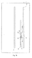
- the encoder device 1 comprises a first terminal 30 for delivery of an electric measurement code signal.
- a detector means 4 is mounted on a first printed circuit board 10 inside the encoder device 1.
- the encoder device 1 further comprises a code means 3 provided with a pattern.
- the code means 3 can be a transparent disc with a pattern that at certain points shadow light from a light source (not shown).
- the detector means 4 and code means 3 being displaceable relative to each other.
- the detector means 4 is disposed to generate an electric measurement code signal in dependence on the relative displacement.
- the detector means 4 includes at least one light-sensitive semiconductor chip 40 which having a first light-sensitive chip surface 47 and a second chip surface 43 on opposing sides.
- the first light-sensitive chip surface 47 has at least one first chip contact area 60 for electrical connection.
- the exemplary embodiment of the encoder device 1 according to the present invention shown in fig. 1 further comprises a second printed circuit board 70 positioned between the detector means 4 and the code means 3.
- the second printed circuit board 70 is shaped so as to allow the passage of light from the code means 3 to the first light-sensitive chip surface 47.
- the second printed circuit board 70 comprises at least one opening 100 so as to allow the passage of light from the code means 3 to the detector means 4.
- a first PCB contact area 80 provided at the second printed circuit board 70 is connected to the terminal 30.
- the first PCB contact area 80 is connected to the first chip contact area 60 by solder, electrically conducting glue or by ohmic contact.
- FIG 1b there is illustrated an assembled view of the exemplary embodiment of the encoder device 1 in figure 1 .
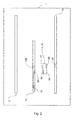
- Figure 2 illustrates yet another exemplary embodiment of the encoder device 1 according to the present invention.
- the first printed circuit board 10 has a second PCB contact area 20 and the second chip surface 43 has a second chip contact area 50 connected to the second PCB contact area 20 by solder, electrically conducting glue or by ohmic contact.
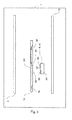
- Figure 3 illustrates yet another exemplary embodiment of the encoder device 1 according to the present invention.
- the second printed circuit board 70 has a second PCB contact area 85 and the first chip surface 47 having a second chip contact 65.
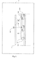
- Figure 4 illustrates a further exemplary embodiment of the encoder device 1 according to the present invention.
- the first printed circuit board 10 further comprises a second terminal 90.
- An electrically conductive device 120 is adapted to provide electrical connection between the second terminal 90 on the first printed circuit board 10 and the first contact area 30 on the second printed circuit board 70.
- the electrically conductive device 120 comprises a flexible body which has a first end which is attached to the first printed circuit board 10 with a first connection and a second end which is attached to the second printed circuit board 70 with a second connection.
- the solder when solder is included, the solder may be substantially free from lead. Lead free soldering requires higher soldering temperature.
- the encoder device 1 further comprises a clamping means when including at least one chip contact area 80, 20 being connected by ohmic contact to a corresponding PCB contact area 50, 60.
- the clamping means is adapted to provide a certain amount of pressure acting to squeeze the second printed circuit board 70 towards the first printed circuit board 10 so as to hold the detector means 4 at a predetermined position between the second printed circuit board 70 and the first printed circuit board 10 such that the ohmic contact is maintained.
- the first printed circuit board 10 may have a shaped portion for positioning the detector means 4 at the predetermined position such that the first chip contact area 50 faces the first PCB contact area 20.
- the first printed circuit board 10 has at least two projections which are protruding from the printed circuit board surface on which the first PCB contact area 20 is located.
- the at least two projections co-operating with a physical shape of the detector means 4 so as to position the detector means 4 at the predetermined position such that the first chip contact area 50 faces the first PCB contact area 20.
- the second chip contact area 50 is connected to the second PCB contact area 20 by solder or electrically conducting glue and the first PCB contact area 80 is connected to the first chip contact area 60 by ohmic contact.
- the electrically conductive device 120 is attached to the first printed circuit board 10 and to the second printed circuit board 70 by solder or electrically conducting glue such that the first printed circuit board 10 co-operates with the second printed circuit board 70 to hold the detector means 4 at a predetermined position between the second printed circuit board 70 and the first printed circuit board 10 such that the ohmic contact is maintained.
- the electrically conductive device 120 comprises a resilient or elastic member adapted to urge the second printed circuit board 70 towards the first printed circuit board 10.
- a further exemplary embodiment of the encoder device 1 according to the present invention comprises a light source arranged and positioned so that the code means 3 is provided in a space between the second printed circuit board 70 and the light source.
- the second printed circuit board 70 has at least one opening which is shaped so as to allow the passage of light to the detector means 4 from a direction of incidence defined by the position of the light source, and wherein the second printed circuit board 70 has a predetermined thickness, the predetermined thickness defining a depth of at least one opening.
- Figure 5 illustrates another exemplary embodiment of the encoder device 1 according to the present invention.
- the encoder device comprises at least a first and a second light-sensitive semiconductor chips 40, 40B adapted to generate the electric measurement code signal so that it vary in dependence on the relative displacement.
- the encoder device further comprises at least one light source 102 being arranged and positioned so that the code means (not shown) is provided in a space between the second printed circuit board 70 and the light source 102.
- the second printed circuit board 70 having at least one opening 100 which is shaped so as to allow the passage of light to the first light-sensitive semiconductor 40.
- the second printed circuit board 70 has a predetermined thickness, the predetermined thickness defining a depth of the at least one opening 100 such that light from the light source 102 is shielded by the second printed circuit board 70 from reaching the second light-sensitive semiconductor chip 40B.
- This solution advantageously reduces or eliminates interference between code signal components originating from detector chips 40, 40B placed adjacent to each other, since this solution provides directivity in that the provision of appropriately shaped openings 100 in the second printed circuit board 70 shields the light. Hence stray light is prevented from hitting the light sensitive surface of an individual chip so that the chip will receive light substantially only via a desired portion of the code means 3.
- Figure 6 illustrates another embodiment of the present invention which relates to an encoder device 1B for optical detection of a change in the intensity of light incident from a direction of incidence.
- the encoder device 1B comprises a first terminal 30 for delivery of an electric measurement code signal and a first printed circuit board 10.
- the encode device 1B further comprises a detector means 4 mounted on the first printed circuit board 10.
- the detector means 4 being disposed to generate the electric measurement signal so that it varies in dependence on the change in light intensity.
- the detector means 4 includes at least one light-sensitive semiconductor chip 40 having a first light-sensitive chip surface 47 and a second chip surface 43 on opposing sides.
- the first light-sensitive chip surface 47 having a first chip contact area 60 for electrical connection.
- a second printed circuit board 70 is positioned between the detector means 4 and the code means 3, wherein the second printed circuit board 70 is shaped so as to allow the passage of light from the direction of incidence to the detector means 4.
- the second printed circuit board 70 has a first PCB contact area 80 connected to the terminal 30, wherein the first PCB contact area 80 is connected to the first chip contact area 60 by solder, electrically conducting glue or by ohmic contact.
- the detector means 4 includes at least two light-sensitive semiconductor chips 40A, 40B.
- the second printed circuit board 70 is shaped so as to allow the passage of light from the direction of incidence to one 40A of the at least two light-sensitive semiconductor chips 40A, 40B) while shielding the one 40A of the at least two light-sensitive semiconductor chips 40A, 40B from light originating from directions deviating from the direction of incidence.
- the second printed circuit board 70 has at least one opening 100 so as to allow the passage of light from the direction of incidence to said detector means 4.
- Figure 7 illustrates a further exemplary embodiment of the encoder device 1B according to the present invention.
- the detector means 4 includes a plurality of light-sensitive semiconductor chips 40, 40A and 40B.
- the second printed circuit board 70 has a plurality of openings 100, 100A, 100B which are shaped so as to allow the passage of light from the direction of incidence to the a plurality of light-sensitive semiconductor chips 40, 40A and 40B.
- the first chip contact area 60 is connected to the first PCB contact area 80 by solder or electrically conducting glue.
- Yet another aspect of the present invention relates to a system for optical detection of a change in the intensity of light.
- the system comprising a light source and at least one encoder device according to any previously described embodiments.
Landscapes
- Physics & Mathematics (AREA)
- General Physics & Mathematics (AREA)
- Optical Transform (AREA)
Claims (16)
- Codierungsvorrichtung (1) zur optischen Erfassung einer Bewegung oder Position, aufweisend:einen ersten Anschluss (30) zur Bereitstellung eines elektrischen Messkodierungssignals (5);eine erste Leiterplatte (10);eine Erfassungseinrichtung (4), die auf der ersten Leiterplatte (10) angebracht ist; undeine Kodierungseinrichtung (3), die mit einem Muster vorgesehen ist; wobei die Erfassungseinrichtung (4) und die Kodierungseinrichtung (3) relativ zueinander versetzbar sind, wobei die Erfassungseinrichtung (4) angeordnet ist, um ein elektrisches Messkodierungssignal in Abhängigkeit von dem relativen Versatz zu erzeugen;wobei die Erfassungseinrichtung (4) umfasst:zumindest einen lichtempfindlichen Halbleiterchip (40) mit einer ersten lichtempfindlichen Chipoberfläche (47) und einer zweiten Chipoberfläche (43) auf gegenüberliegenden Seiten;wobei die erste lichtempfindliche Chipoberfläche (47) ein erstes Chipkontaktgebiet (60) zur elektrischen Verbindung aufweist; undeine zweite Leiterplatte (70), die zwischen der Erfassungseinrichtung (4) und der Kodierungseinrichtung (3) positioniert ist, wobei
die zweite Leiterplatte (70) so geformt ist, um den Durchtritt von Licht von der Kodierungseinrichtung (3) zu der ersten lichtempfindlichen Chipoberfläche (47) zu ermöglichen, und
die zweite Leiterplatte (70) ein erstes PCB-Kontaktgebiet (80) aufweist, das mit einem Anschluss (30) verbunden ist, wobei der Anschluss (30) auf der zweiten Leiterplatte (70) angeordnet ist; wobei das erste PCB-Kontaktgebiet (80) mit dem ersten Chipkontaktgebiet (60) durch ein Lötmittel, elektrisch leitenden Klebstoff oder durch einen ohmschen Kontakt verbunden ist. - Codierungsvorrichtung (1) nach Anspruch 1, wobei die erste Leiterplatte (10) ein zweites PCB-Kontaktgebiet (20) aufweist; und
die zweite Chipoberfläche (43) ein zweites Chipkontaktgebiet (50) aufweist, das mit dem zweiten PCB-Kontaktgebiet (20) durch ein Lötmittel, elektrisch leitenden Klebstoff oder durch einen ohmschen Kontakt verbunden ist. - Codierungsvorrichtung (1) nach Anspruch 1, wobei die zweite Leiterplatte (70) ein zweites PCB-Kontaktgebiet (65) aufweist; und
die erste Chipoberfläche (47) ein zweites Chipkontaktgebiet (50) aufweist, das mit dem zweiten PCB-Kontaktgebiet (65) durch ein Lötmittel, elektrisch leitenden Klebstoff oder durch einen ohmschen Kontakt verbunden ist. - Codierungsvorrichtung (1) nach einem der Ansprüche 1 bis 3, wobei
ein zweiter Anschluss (90B) auf der ersten Leiterplatte (10) vorgesehen ist, wobei die Codierungsvorrichtung (1) ferner aufweist:eine elektrisch leitende Vorrichtung (120), die angepasst ist, um eine elektrische Verbindung zwischen dem zweiten Anschluss (90B) auf der ersten Leiterplatte (10) und einem zweiten PCB-Kontaktgebiet (90) auf der zweiten Leiterplatte (70) vorzusehen. - Codierungsvorrichtung (1) nach Anspruch 4, wobei
die elektrisch leitende Vorrichtung (120) einen im Wesentlichen steifen Körper (120) aufweist, der zwischen der ersten Leiterplatte (10) und der zweiten Leiterplatte (70) positioniert ist, und wobei
die elektrische Verbindung zwischen der ersten Leiterplatte (10) und der zweiten Leiterplatte (70) über die elektrisch leitende Vorrichtung (120) angepasst ist, um ein Lötmittel, elektrisch leitenden Klebstoff oder einen ohmschen Kontakt zu umfassen. - Codierungsvorrichtung (1) nach Anspruch 4, wobei die elektrisch leitende Vorrichtung (120) einen flexiblen Körper aufweist, mit:einem ersten Ende, das an der ersten Leiterplatte (10) mit einer ersten Verbindung angebracht ist, undeinem zweiten Ende, das an der zweiten Leiterplatte (70) mit einer zweiten Verbindung angebracht ist.
- Codierungsvorrichtung (1) nach einem der vorangehenden Ansprüche, wobei die zweite Leiterplatte (70) aufweist:zumindest eine Öffnung (100), um den Durchtritt von Licht von der Kodierungseinrichtung (3) zu der Erfassungseinrichtung (4) zu ermöglichen.
- Codierungsvorrichtung (1) nach einem der vorangehenden Ansprüche, wenn zumindest ein Chipkontaktgebiet (50, 60) umfasst ist, das durch einen ohmschen Kontakt mit einem korrespondierenden PCB-Kontaktgebiet (20, 80) verbunden ist, ferner aufweisend:eine Klemmeinrichtung, die angepasst ist, um eine bestimmte Menge an Druck vorzusehen, um die zweite Leiterplatte (70) in Richtung der ersten Leiterplatte (10) zu drücken, damit die Erfassungseinrichtung (4) an einer vorbestimmten Position zwischen der zweiten Leiterplatte (70) und der ersten Leiterplatte (10) derart gehalten wird, dass der ohmsche Kontakt aufrechterhalten wird.
- Codierungsvorrichtung (1) nach Anspruch 8, wobei
die erste Leiterplatte (10) einen geformten Abschnitt zur Positionierung der Erfassungseinrichtung (4) an der vorbestimmten Position derart aufweist, dass das erste Chipkontaktgebiet (50) dem ersten PCB-Kontaktgebiet (20) zugewandt ist. - Codierungsvorrichtung (1) nach Anspruch 8 oder 9, wobei
die erste Leiterplatte (10) zumindest zwei Vorsprünge aufweist, welche von der Leiterplattenoberfläche vorstehen, auf welcher das erste PCB-Kontaktgebiet (20) angeordnet ist; wobei die zumindest zwei Vorsprünge mit einer physikalischen Form der Erfassungseinrichtung (4) zusammenwirken, damit die Erfassungseinrichtung (4) an der vorbestimmten Position derart positioniert wird, dass das erste Chipkontaktgebiet (50) dem ersten PCB-Kontaktgebiet (20) zugewandt ist. - Codierungsvorrichtung (1) nach einem der vorangehenden Ansprüche, wobei
das zweite Chipkontaktgebiet (50) mit dem zweiten PCB-Kontaktgebiet (20) durch ein Lötmittel oder elektrisch leitenden Klebstoff verbunden ist; und wobei
das erste PCB-Kontaktgebiet (80) mit dem ersten Chipkontaktgebiet (60) durch einen ohmschen Kontakt verbunden ist. - Codierungsvorrichtung (1) nach Anspruch 4, wobei
die elektrisch leitende Vorrichtung (120) an der ersten Leiterplatte (10) und an der zweiten Leiterplatte (70) durch ein Lötmittel oder elektrisch leitenden Klebstoff derart angebracht ist, dass die erste Leiterplatte (10) mit der zweiten Leiterplatte (70) zusammenwirkt, um die Erfassungseinrichtung (4) an einer vorbestimmten Position zwischen der zweiten Leiterplatte (70) und der ersten Leiterplatte (10) derart zu halten, dass ein ohmscher Kontakt aufrechterhalten wird. - Codierungsvorrichtung (1) nach Anspruch 12, wobei
die elektrisch leitende Vorrichtung (120) ein nachgiebiges oder elastisches Element aufweist, das angepasst ist, um die zweite Leiterplatte (70) in Richtung der ersten Leiterplatte (10) zu drängen. - Codierungsvorrichtung (1) nach einem der vorangehenden Ansprüche, ferner aufweisend:eine Lichtquelle (102), die so angeordnet und positioniert ist, dass die Codierungseinrichtung (3) in einem Raum zwischen der zweiten Leiterplatte (70) und der Lichtquelle (102) vorgesehen ist.
- Codierungsvorrichtung (1) nach Anspruch 14, wobei die zweite Leiterplatte (70) zumindest eine Öffnung (100) aufweist, welche so geformt ist, um den Durchtritt von Licht zu der Erfassungseinrichtung (4) von einer Einfallsrichtung, die durch die Position der Lichtquelle (102) definiert ist, zu ermöglichen, und wobei
die zweite Leiterplatte (70) eine vorbestimmte Dicke aufweist, wobei die vorbestimmte Dicke eine Tiefe von zumindest einer Öffnung (100) definiert. - Codierungsvorrichtung (1) nach einem der vorangehenden Ansprüche, wobei
die Erfassungseinrichtung (4) umfasst:zumindest einen ersten und einen zweiten lichtempfindlichen Halbleiterchip (40, 40B), die angepasst sind, um das elektrische Messkodierungssignal so zu erzeugen, dass es in Abhängigkeit von dem relativen Versatz variieren kann; wobei die Codierungsvorrichtung ferner aufweist:die zweite Leiterplatte (70) zumindest eine Öffnung (100) aufweist, welche so geformt ist, dass der Durchtritt von Licht zu dem ersten lichtempfindlichen Halbleiter (40) ermöglicht wird; und wobeizumindest eine Lichtquelle (102), die so angeordnet und positioniert ist, dass die Codierungseinrichtung (3) in einem Raum zwischen der zweiten Leiterplatte (70) und der Lichtquelle (102) vorgesehen ist; und
die zweite Leiterplatte (70) eine vorbestimmte Dicke aufweist, wobei die vorbestimmte Dicke eine Tiefe von zumindest einer Öffnung (100) derart definiert, dass Licht von der Lichtquelle (102) durch die zweite Leiterplatte (70) von einem Erreichen des zweiten lichtempfindlichen Halbleiterchips (40B) abgeschirmt wird.
Applications Claiming Priority (1)
| Application Number | Priority Date | Filing Date | Title |
|---|---|---|---|
| SE1250642A SE537200C2 (sv) | 2012-06-18 | 2012-06-18 | Pulsgivaranordning för optisk detektering av rörelse eller läge |
Publications (2)
| Publication Number | Publication Date |
|---|---|
| EP2677282A1 EP2677282A1 (de) | 2013-12-25 |
| EP2677282B1 true EP2677282B1 (de) | 2015-06-24 |
Family
ID=48537824
Family Applications (1)
| Application Number | Title | Priority Date | Filing Date |
|---|---|---|---|
| EP13169704.7A Active EP2677282B1 (de) | 2012-06-18 | 2013-05-29 | Codierungsvorrichtung zur optischen Detektion von Bewegung oder Position |
Country Status (3)
| Country | Link |
|---|---|
| US (1) | US9304016B2 (de) |
| EP (1) | EP2677282B1 (de) |
| SE (1) | SE537200C2 (de) |
Families Citing this family (1)
| Publication number | Priority date | Publication date | Assignee | Title |
|---|---|---|---|---|
| US10315914B2 (en) * | 2016-06-27 | 2019-06-11 | The Charles Stark Draper Laboratory, Inc. | Reconstructed wafer based devices with embedded environmental sensors and process for making same |
Family Cites Families (5)
| Publication number | Priority date | Publication date | Assignee | Title |
|---|---|---|---|---|
| US4703176A (en) * | 1985-06-04 | 1987-10-27 | Plus Development Corporation | Compact polyphase optical position encoder |
| ES2153823T3 (es) * | 1992-04-08 | 2001-03-16 | Heidenhain Gmbh Dr Johannes | Captador optoelectronico para la medicion del recorrido; del angulo o de la rotacion. |
| US5670781B1 (en) * | 1996-02-08 | 2000-10-10 | Renco Encoders Inc | Photoelectrical encoder |
| DE19855828A1 (de) * | 1998-12-03 | 2000-06-08 | Heidenhain Gmbh Dr Johannes | Dreidimensionales Meßmodul |
| US7244928B2 (en) * | 2005-01-07 | 2007-07-17 | Avago Technologies Ecbu Ip (Singapore) Pte. Ltd. | Optical encoder |
-
2012
- 2012-06-18 SE SE1250642A patent/SE537200C2/sv not_active IP Right Cessation
-
2013
- 2013-05-29 EP EP13169704.7A patent/EP2677282B1/de active Active
- 2013-06-18 US US13/920,733 patent/US9304016B2/en active Active
Also Published As
| Publication number | Publication date |
|---|---|
| SE1250642A1 (sv) | 2013-12-19 |
| US9304016B2 (en) | 2016-04-05 |
| SE537200C2 (sv) | 2015-03-03 |
| EP2677282A1 (de) | 2013-12-25 |
| US20130341499A1 (en) | 2013-12-26 |
Similar Documents
| Publication | Publication Date | Title |
|---|---|---|
| US8866064B2 (en) | Multi-directional proximity sensor | |
| CN103383470B (zh) | 用于光幕的光学模块和光学单元以及制造方法 | |
| TWI447612B (zh) | 具有至少一感光器電路的光電模組 | |
| US10627262B2 (en) | Sensor unit for position measurement | |
| EP2677282B1 (de) | Codierungsvorrichtung zur optischen Detektion von Bewegung oder Position | |
| US10260909B2 (en) | Position measuring device | |
| US10670430B2 (en) | Sensor | |
| US10378932B2 (en) | Sensor having generating and detecting units on a substrate with a curve or bent shape in a cylindrical housing and method of manufacturing sensor | |
| US7518157B2 (en) | Optoelectronic component assembly | |
| US10337892B2 (en) | Sensor and method of manufacturing sensor | |
| KR102644801B1 (ko) | 접촉 챔버를 갖는 이송 장치를 포함하는 광전자 장치 | |
| US10458817B2 (en) | Sensor manufacturing method and sensor | |
| CN110676366A (zh) | 位置测量装置及其传感器单元的光源的制造方法 | |
| CN110676365A (zh) | 用于制造用于位置测量装置的传感器单元的光源的方法以及位置测量装置 | |
| JP6896157B2 (ja) | センサ部品、センサ部品の事前組立て構成およびセンサ部品の製造方法 | |
| US10139252B2 (en) | Optical sensor | |
| JP2006078376A (ja) | 光学式変位センサ | |
| US20040211890A1 (en) | Positional encoder assembly | |
| JP7645687B2 (ja) | 光学センサ | |
| US9829351B2 (en) | Encoding device | |
| US9025968B2 (en) | Optical communication device | |
| JP7514101B2 (ja) | 光源、その製造方法および光源を備える位置測定装置 | |
| US11231298B2 (en) | Sensor, sensor substrate, and sensor manufacturing method | |
| JP2021042963A (ja) | 物理量センサの製造方法 | |
| JP2017125703A (ja) | 光センサ、ロータリエンコーダ及び光センサの製造方法 |
Legal Events
| Date | Code | Title | Description |
|---|---|---|---|
| PUAI | Public reference made under article 153(3) epc to a published international application that has entered the european phase |
Free format text: ORIGINAL CODE: 0009012 |
|
| AK | Designated contracting states |
Kind code of ref document: A1 Designated state(s): AL AT BE BG CH CY CZ DE DK EE ES FI FR GB GR HR HU IE IS IT LI LT LU LV MC MK MT NL NO PL PT RO RS SE SI SK SM TR |
|
| AX | Request for extension of the european patent |
Extension state: BA ME |
|
| 17P | Request for examination filed |
Effective date: 20140617 |
|
| RBV | Designated contracting states (corrected) |
Designated state(s): AL AT BE BG CH CY CZ DE DK EE ES FI FR GB GR HR HU IE IS IT LI LT LU LV MC MK MT NL NO PL PT RO RS SE SI SK SM TR |
|
| GRAP | Despatch of communication of intention to grant a patent |
Free format text: ORIGINAL CODE: EPIDOSNIGR1 |
|
| INTG | Intention to grant announced |
Effective date: 20141223 |
|
| GRAS | Grant fee paid |
Free format text: ORIGINAL CODE: EPIDOSNIGR3 |
|
| GRAA | (expected) grant |
Free format text: ORIGINAL CODE: 0009210 |
|
| AK | Designated contracting states |
Kind code of ref document: B1 Designated state(s): AL AT BE BG CH CY CZ DE DK EE ES FI FR GB GR HR HU IE IS IT LI LT LU LV MC MK MT NL NO PL PT RO RS SE SI SK SM TR |
|
| REG | Reference to a national code |
Ref country code: GB Ref legal event code: FG4D |
|
| REG | Reference to a national code |
Ref country code: CH Ref legal event code: EP |
|
| REG | Reference to a national code |
Ref country code: AT Ref legal event code: REF Ref document number: 733102 Country of ref document: AT Kind code of ref document: T Effective date: 20150715 |
|
| REG | Reference to a national code |
Ref country code: SE Ref legal event code: TRGR |
|
| REG | Reference to a national code |
Ref country code: IE Ref legal event code: FG4D |
|
| REG | Reference to a national code |
Ref country code: DE Ref legal event code: R096 Ref document number: 602013002065 Country of ref document: DE |
|
| REG | Reference to a national code |
Ref country code: CH Ref legal event code: NV Representative=s name: ISLER AND PEDRAZZINI AG, CH |
|
| PG25 | Lapsed in a contracting state [announced via postgrant information from national office to epo] |
Ref country code: HR Free format text: LAPSE BECAUSE OF FAILURE TO SUBMIT A TRANSLATION OF THE DESCRIPTION OR TO PAY THE FEE WITHIN THE PRESCRIBED TIME-LIMIT Effective date: 20150624 Ref country code: LT Free format text: LAPSE BECAUSE OF FAILURE TO SUBMIT A TRANSLATION OF THE DESCRIPTION OR TO PAY THE FEE WITHIN THE PRESCRIBED TIME-LIMIT Effective date: 20150624 Ref country code: NO Free format text: LAPSE BECAUSE OF FAILURE TO SUBMIT A TRANSLATION OF THE DESCRIPTION OR TO PAY THE FEE WITHIN THE PRESCRIBED TIME-LIMIT Effective date: 20150924 |
|
| REG | Reference to a national code |
Ref country code: AT Ref legal event code: MK05 Ref document number: 733102 Country of ref document: AT Kind code of ref document: T Effective date: 20150624 |
|
| REG | Reference to a national code |
Ref country code: LT Ref legal event code: MG4D |
|
| PG25 | Lapsed in a contracting state [announced via postgrant information from national office to epo] |
Ref country code: BG Free format text: LAPSE BECAUSE OF FAILURE TO SUBMIT A TRANSLATION OF THE DESCRIPTION OR TO PAY THE FEE WITHIN THE PRESCRIBED TIME-LIMIT Effective date: 20150924 Ref country code: LV Free format text: LAPSE BECAUSE OF FAILURE TO SUBMIT A TRANSLATION OF THE DESCRIPTION OR TO PAY THE FEE WITHIN THE PRESCRIBED TIME-LIMIT Effective date: 20150624 Ref country code: RS Free format text: LAPSE BECAUSE OF FAILURE TO SUBMIT A TRANSLATION OF THE DESCRIPTION OR TO PAY THE FEE WITHIN THE PRESCRIBED TIME-LIMIT Effective date: 20150624 Ref country code: GR Free format text: LAPSE BECAUSE OF FAILURE TO SUBMIT A TRANSLATION OF THE DESCRIPTION OR TO PAY THE FEE WITHIN THE PRESCRIBED TIME-LIMIT Effective date: 20150925 |
|
| REG | Reference to a national code |
Ref country code: NL Ref legal event code: MP Effective date: 20150624 |
|
| PG25 | Lapsed in a contracting state [announced via postgrant information from national office to epo] |
Ref country code: EE Free format text: LAPSE BECAUSE OF FAILURE TO SUBMIT A TRANSLATION OF THE DESCRIPTION OR TO PAY THE FEE WITHIN THE PRESCRIBED TIME-LIMIT Effective date: 20150624 |
|
| PG25 | Lapsed in a contracting state [announced via postgrant information from national office to epo] |
Ref country code: CZ Free format text: LAPSE BECAUSE OF FAILURE TO SUBMIT A TRANSLATION OF THE DESCRIPTION OR TO PAY THE FEE WITHIN THE PRESCRIBED TIME-LIMIT Effective date: 20150624 Ref country code: PL Free format text: LAPSE BECAUSE OF FAILURE TO SUBMIT A TRANSLATION OF THE DESCRIPTION OR TO PAY THE FEE WITHIN THE PRESCRIBED TIME-LIMIT Effective date: 20150624 Ref country code: SK Free format text: LAPSE BECAUSE OF FAILURE TO SUBMIT A TRANSLATION OF THE DESCRIPTION OR TO PAY THE FEE WITHIN THE PRESCRIBED TIME-LIMIT Effective date: 20150624 Ref country code: RO Free format text: LAPSE BECAUSE OF NON-PAYMENT OF DUE FEES Effective date: 20150624 Ref country code: PT Free format text: LAPSE BECAUSE OF FAILURE TO SUBMIT A TRANSLATION OF THE DESCRIPTION OR TO PAY THE FEE WITHIN THE PRESCRIBED TIME-LIMIT Effective date: 20151026 Ref country code: ES Free format text: LAPSE BECAUSE OF FAILURE TO SUBMIT A TRANSLATION OF THE DESCRIPTION OR TO PAY THE FEE WITHIN THE PRESCRIBED TIME-LIMIT Effective date: 20150624 Ref country code: AT Free format text: LAPSE BECAUSE OF FAILURE TO SUBMIT A TRANSLATION OF THE DESCRIPTION OR TO PAY THE FEE WITHIN THE PRESCRIBED TIME-LIMIT Effective date: 20150624 Ref country code: IS Free format text: LAPSE BECAUSE OF FAILURE TO SUBMIT A TRANSLATION OF THE DESCRIPTION OR TO PAY THE FEE WITHIN THE PRESCRIBED TIME-LIMIT Effective date: 20151024 |
|
| REG | Reference to a national code |
Ref country code: DE Ref legal event code: R097 Ref document number: 602013002065 Country of ref document: DE |
|
| PG25 | Lapsed in a contracting state [announced via postgrant information from national office to epo] |
Ref country code: DK Free format text: LAPSE BECAUSE OF FAILURE TO SUBMIT A TRANSLATION OF THE DESCRIPTION OR TO PAY THE FEE WITHIN THE PRESCRIBED TIME-LIMIT Effective date: 20150624 |
|
| PLBE | No opposition filed within time limit |
Free format text: ORIGINAL CODE: 0009261 |
|
| STAA | Information on the status of an ep patent application or granted ep patent |
Free format text: STATUS: NO OPPOSITION FILED WITHIN TIME LIMIT |
|
| 26N | No opposition filed |
Effective date: 20160329 |
|
| PG25 | Lapsed in a contracting state [announced via postgrant information from national office to epo] |
Ref country code: BE Free format text: LAPSE BECAUSE OF NON-PAYMENT OF DUE FEES Effective date: 20160531 Ref country code: SI Free format text: LAPSE BECAUSE OF FAILURE TO SUBMIT A TRANSLATION OF THE DESCRIPTION OR TO PAY THE FEE WITHIN THE PRESCRIBED TIME-LIMIT Effective date: 20150624 |
|
| PG25 | Lapsed in a contracting state [announced via postgrant information from national office to epo] |
Ref country code: LU Free format text: LAPSE BECAUSE OF FAILURE TO SUBMIT A TRANSLATION OF THE DESCRIPTION OR TO PAY THE FEE WITHIN THE PRESCRIBED TIME-LIMIT Effective date: 20160529 Ref country code: BE Free format text: LAPSE BECAUSE OF FAILURE TO SUBMIT A TRANSLATION OF THE DESCRIPTION OR TO PAY THE FEE WITHIN THE PRESCRIBED TIME-LIMIT Effective date: 20150624 |
|
| REG | Reference to a national code |
Ref country code: IE Ref legal event code: MM4A |
|
| REG | Reference to a national code |
Ref country code: FR Ref legal event code: ST Effective date: 20170131 |
|
| PG25 | Lapsed in a contracting state [announced via postgrant information from national office to epo] |
Ref country code: FR Free format text: LAPSE BECAUSE OF NON-PAYMENT OF DUE FEES Effective date: 20160531 |
|
| PG25 | Lapsed in a contracting state [announced via postgrant information from national office to epo] |
Ref country code: IE Free format text: LAPSE BECAUSE OF NON-PAYMENT OF DUE FEES Effective date: 20160529 |
|
| PG25 | Lapsed in a contracting state [announced via postgrant information from national office to epo] |
Ref country code: NL Free format text: LAPSE BECAUSE OF FAILURE TO SUBMIT A TRANSLATION OF THE DESCRIPTION OR TO PAY THE FEE WITHIN THE PRESCRIBED TIME-LIMIT Effective date: 20150624 |
|
| PG25 | Lapsed in a contracting state [announced via postgrant information from national office to epo] |
Ref country code: SM Free format text: LAPSE BECAUSE OF FAILURE TO SUBMIT A TRANSLATION OF THE DESCRIPTION OR TO PAY THE FEE WITHIN THE PRESCRIBED TIME-LIMIT Effective date: 20150624 Ref country code: CY Free format text: LAPSE BECAUSE OF FAILURE TO SUBMIT A TRANSLATION OF THE DESCRIPTION OR TO PAY THE FEE WITHIN THE PRESCRIBED TIME-LIMIT Effective date: 20150624 Ref country code: HU Free format text: LAPSE BECAUSE OF FAILURE TO SUBMIT A TRANSLATION OF THE DESCRIPTION OR TO PAY THE FEE WITHIN THE PRESCRIBED TIME-LIMIT; INVALID AB INITIO Effective date: 20130529 |
|
| PG25 | Lapsed in a contracting state [announced via postgrant information from national office to epo] |
Ref country code: MT Free format text: LAPSE BECAUSE OF NON-PAYMENT OF DUE FEES Effective date: 20160531 Ref country code: TR Free format text: LAPSE BECAUSE OF FAILURE TO SUBMIT A TRANSLATION OF THE DESCRIPTION OR TO PAY THE FEE WITHIN THE PRESCRIBED TIME-LIMIT Effective date: 20150624 Ref country code: MK Free format text: LAPSE BECAUSE OF FAILURE TO SUBMIT A TRANSLATION OF THE DESCRIPTION OR TO PAY THE FEE WITHIN THE PRESCRIBED TIME-LIMIT Effective date: 20150624 Ref country code: MC Free format text: LAPSE BECAUSE OF FAILURE TO SUBMIT A TRANSLATION OF THE DESCRIPTION OR TO PAY THE FEE WITHIN THE PRESCRIBED TIME-LIMIT Effective date: 20150624 |
|
| PG25 | Lapsed in a contracting state [announced via postgrant information from national office to epo] |
Ref country code: AL Free format text: LAPSE BECAUSE OF FAILURE TO SUBMIT A TRANSLATION OF THE DESCRIPTION OR TO PAY THE FEE WITHIN THE PRESCRIBED TIME-LIMIT Effective date: 20150624 |
|
| PGFP | Annual fee paid to national office [announced via postgrant information from national office to epo] |
Ref country code: FI Payment date: 20250526 Year of fee payment: 13 |
|
| PGFP | Annual fee paid to national office [announced via postgrant information from national office to epo] |
Ref country code: DE Payment date: 20250521 Year of fee payment: 13 |
|
| PGFP | Annual fee paid to national office [announced via postgrant information from national office to epo] |
Ref country code: GB Payment date: 20250521 Year of fee payment: 13 |
|
| PGFP | Annual fee paid to national office [announced via postgrant information from national office to epo] |
Ref country code: IT Payment date: 20250527 Year of fee payment: 13 |
|
| PGFP | Annual fee paid to national office [announced via postgrant information from national office to epo] |
Ref country code: CH Payment date: 20250601 Year of fee payment: 13 |
|
| PGFP | Annual fee paid to national office [announced via postgrant information from national office to epo] |
Ref country code: SE Payment date: 20250521 Year of fee payment: 13 |