EP2674981A1 - Active matrix substrate, display panel, and display device - Google Patents
Active matrix substrate, display panel, and display device Download PDFInfo
- Publication number
- EP2674981A1 EP2674981A1 EP12745003.9A EP12745003A EP2674981A1 EP 2674981 A1 EP2674981 A1 EP 2674981A1 EP 12745003 A EP12745003 A EP 12745003A EP 2674981 A1 EP2674981 A1 EP 2674981A1
- Authority
- EP
- European Patent Office
- Prior art keywords
- active matrix
- matrix substrate
- electrode
- drain electrode
- layer
- Prior art date
- Legal status (The legal status is an assumption and is not a legal conclusion. Google has not performed a legal analysis and makes no representation as to the accuracy of the status listed.)
- Withdrawn
Links
Images







Classifications
-
- H—ELECTRICITY
- H10—SEMICONDUCTOR DEVICES; ELECTRIC SOLID-STATE DEVICES NOT OTHERWISE PROVIDED FOR
- H10D—INORGANIC ELECTRIC SEMICONDUCTOR DEVICES
- H10D86/00—Integrated devices formed in or on insulating or conducting substrates, e.g. formed in silicon-on-insulator [SOI] substrates or on stainless steel or glass substrates
- H10D86/40—Integrated devices formed in or on insulating or conducting substrates, e.g. formed in silicon-on-insulator [SOI] substrates or on stainless steel or glass substrates characterised by multiple TFTs
- H10D86/60—Integrated devices formed in or on insulating or conducting substrates, e.g. formed in silicon-on-insulator [SOI] substrates or on stainless steel or glass substrates characterised by multiple TFTs wherein the TFTs are in active matrices
-
- H—ELECTRICITY
- H10—SEMICONDUCTOR DEVICES; ELECTRIC SOLID-STATE DEVICES NOT OTHERWISE PROVIDED FOR
- H10D—INORGANIC ELECTRIC SEMICONDUCTOR DEVICES
- H10D30/00—Field-effect transistors [FET]
- H10D30/60—Insulated-gate field-effect transistors [IGFET]
- H10D30/67—Thin-film transistors [TFT]
- H10D30/6729—Thin-film transistors [TFT] characterised by the electrodes
-
- H—ELECTRICITY
- H10—SEMICONDUCTOR DEVICES; ELECTRIC SOLID-STATE DEVICES NOT OTHERWISE PROVIDED FOR
- H10D—INORGANIC ELECTRIC SEMICONDUCTOR DEVICES
- H10D30/00—Field-effect transistors [FET]
- H10D30/01—Manufacture or treatment
- H10D30/021—Manufacture or treatment of FETs having insulated gates [IGFET]
- H10D30/031—Manufacture or treatment of FETs having insulated gates [IGFET] of thin-film transistors [TFT]
- H10D30/0312—Manufacture or treatment of FETs having insulated gates [IGFET] of thin-film transistors [TFT] characterised by the gate electrodes
- H10D30/0316—Manufacture or treatment of FETs having insulated gates [IGFET] of thin-film transistors [TFT] characterised by the gate electrodes of lateral bottom-gate TFTs comprising only a single gate
-
- H—ELECTRICITY
- H10—SEMICONDUCTOR DEVICES; ELECTRIC SOLID-STATE DEVICES NOT OTHERWISE PROVIDED FOR
- H10D—INORGANIC ELECTRIC SEMICONDUCTOR DEVICES
- H10D30/00—Field-effect transistors [FET]
- H10D30/01—Manufacture or treatment
- H10D30/021—Manufacture or treatment of FETs having insulated gates [IGFET]
- H10D30/031—Manufacture or treatment of FETs having insulated gates [IGFET] of thin-film transistors [TFT]
- H10D30/0321—Manufacture or treatment of FETs having insulated gates [IGFET] of thin-film transistors [TFT] comprising silicon, e.g. amorphous silicon or polysilicon
-
- H—ELECTRICITY
- H10—SEMICONDUCTOR DEVICES; ELECTRIC SOLID-STATE DEVICES NOT OTHERWISE PROVIDED FOR
- H10D—INORGANIC ELECTRIC SEMICONDUCTOR DEVICES
- H10D30/00—Field-effect transistors [FET]
- H10D30/60—Insulated-gate field-effect transistors [IGFET]
- H10D30/67—Thin-film transistors [TFT]
- H10D30/6729—Thin-film transistors [TFT] characterised by the electrodes
- H10D30/6737—Thin-film transistors [TFT] characterised by the electrodes characterised by the electrode materials
-
- H—ELECTRICITY
- H10—SEMICONDUCTOR DEVICES; ELECTRIC SOLID-STATE DEVICES NOT OTHERWISE PROVIDED FOR
- H10D—INORGANIC ELECTRIC SEMICONDUCTOR DEVICES
- H10D30/00—Field-effect transistors [FET]
- H10D30/60—Insulated-gate field-effect transistors [IGFET]
- H10D30/67—Thin-film transistors [TFT]
- H10D30/6729—Thin-film transistors [TFT] characterised by the electrodes
- H10D30/6737—Thin-film transistors [TFT] characterised by the electrodes characterised by the electrode materials
- H10D30/6739—Conductor-insulator-semiconductor electrodes
-
- H—ELECTRICITY
- H10—SEMICONDUCTOR DEVICES; ELECTRIC SOLID-STATE DEVICES NOT OTHERWISE PROVIDED FOR
- H10D—INORGANIC ELECTRIC SEMICONDUCTOR DEVICES
- H10D30/00—Field-effect transistors [FET]
- H10D30/60—Insulated-gate field-effect transistors [IGFET]
- H10D30/67—Thin-film transistors [TFT]
- H10D30/674—Thin-film transistors [TFT] characterised by the active materials
- H10D30/6741—Group IV materials, e.g. germanium or silicon carbide
- H10D30/6743—Silicon
-
- H—ELECTRICITY
- H10—SEMICONDUCTOR DEVICES; ELECTRIC SOLID-STATE DEVICES NOT OTHERWISE PROVIDED FOR
- H10D—INORGANIC ELECTRIC SEMICONDUCTOR DEVICES
- H10D30/00—Field-effect transistors [FET]
- H10D30/60—Insulated-gate field-effect transistors [IGFET]
- H10D30/67—Thin-film transistors [TFT]
- H10D30/674—Thin-film transistors [TFT] characterised by the active materials
- H10D30/6755—Oxide semiconductors, e.g. zinc oxide, copper aluminium oxide or cadmium stannate
-
- H—ELECTRICITY
- H10—SEMICONDUCTOR DEVICES; ELECTRIC SOLID-STATE DEVICES NOT OTHERWISE PROVIDED FOR
- H10D—INORGANIC ELECTRIC SEMICONDUCTOR DEVICES
- H10D64/00—Electrodes of devices having potential barriers
- H10D64/60—Electrodes characterised by their materials
- H10D64/62—Electrodes ohmically coupled to a semiconductor
-
- H—ELECTRICITY
- H10—SEMICONDUCTOR DEVICES; ELECTRIC SOLID-STATE DEVICES NOT OTHERWISE PROVIDED FOR
- H10D—INORGANIC ELECTRIC SEMICONDUCTOR DEVICES
- H10D86/00—Integrated devices formed in or on insulating or conducting substrates, e.g. formed in silicon-on-insulator [SOI] substrates or on stainless steel or glass substrates
- H10D86/40—Integrated devices formed in or on insulating or conducting substrates, e.g. formed in silicon-on-insulator [SOI] substrates or on stainless steel or glass substrates characterised by multiple TFTs
- H10D86/441—Interconnections, e.g. scanning lines
- H10D86/443—Interconnections, e.g. scanning lines adapted for preventing breakage, peeling or short circuiting
-
- H—ELECTRICITY
- H10—SEMICONDUCTOR DEVICES; ELECTRIC SOLID-STATE DEVICES NOT OTHERWISE PROVIDED FOR
- H10D—INORGANIC ELECTRIC SEMICONDUCTOR DEVICES
- H10D99/00—Subject matter not provided for in other groups of this subclass
-
- G—PHYSICS
- G02—OPTICS
- G02F—OPTICAL DEVICES OR ARRANGEMENTS FOR THE CONTROL OF LIGHT BY MODIFICATION OF THE OPTICAL PROPERTIES OF THE MEDIA OF THE ELEMENTS INVOLVED THEREIN; NON-LINEAR OPTICS; FREQUENCY-CHANGING OF LIGHT; OPTICAL LOGIC ELEMENTS; OPTICAL ANALOGUE/DIGITAL CONVERTERS
- G02F1/00—Devices or arrangements for the control of the intensity, colour, phase, polarisation or direction of light arriving from an independent light source, e.g. switching, gating or modulating; Non-linear optics
- G02F1/01—Devices or arrangements for the control of the intensity, colour, phase, polarisation or direction of light arriving from an independent light source, e.g. switching, gating or modulating; Non-linear optics for the control of the intensity, phase, polarisation or colour
- G02F1/13—Devices or arrangements for the control of the intensity, colour, phase, polarisation or direction of light arriving from an independent light source, e.g. switching, gating or modulating; Non-linear optics for the control of the intensity, phase, polarisation or colour based on liquid crystals, e.g. single liquid crystal display cells
- G02F1/133—Constructional arrangements; Operation of liquid crystal cells; Circuit arrangements
- G02F1/136—Liquid crystal cells structurally associated with a semi-conducting layer or substrate, e.g. cells forming part of an integrated circuit
- G02F1/1362—Active matrix addressed cells
- G02F1/1368—Active matrix addressed cells in which the switching element is a three-electrode device
Definitions
- the present invention relates to an active matrix substrate including thin film transistors, and a display panel and a display device each of which includes the active matrix substrate.
- liquid crystal display devices have rapidly become popular because they consume less electric power and are more easily downsized than CRTs (Cathode-Ray-Tubes).
- CRTs Cathode-Ray-Tubes
- active matrix liquid crystal display devices which respond at high speed and easily carry out multi-gradation display, have been in widespread use.
- An active matrix liquid crystal display device includes (i) an active matrix substrate in which a plurality of pixels are arranged in a matrix manner, (ii) a counter substrate provided so as to face the active matrix substrate and (iii) a liquid crystal layer which is a display medium and sandwiched between the active matrix substrate and the counter substrate.
- a plurality of scanning lines and a plurality of signal lines are provided so as to intersect with each other, and pixel sections each including a thin film transistor (TFT) are provided in the vicinity of respective parts in which the plurality of scanning lines intersect with the plurality of signal lines.
- TFT thin film transistor
- Patent Literature 1 describes an array substrate for use in a liquid crystal display device, which array substrate includes (i) a first ohmic contact layer and a second ohmic contact layer which are provided on an active layer so as to separate from each other by a first distance, (ii) a first barrier pattern and a second barrier pattern which are provided on the first ohmic contact layer and the second ohmic contact layer, respectively, so as to separate from each other by the first distance so that the active layer is exposed between the first barrier pattern and the second barrier pattern and (iii) a source electrode and a drain electrode which are provided on the first barrier pattern and the second barrier pattern, respectively, so as to separate from each other by a second distance that is larger than the first distance, the source electrode being connected to a corresponding data line.
- Patent Literature 1 Japanese Patent Application Publication, Tokukai, No. 2008-166789 A (Publication Date: July 17, 2008 )
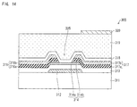
- Fig. 14 is a cross-sectional view partially illustrating the conventional active matrix substrate. Specifically, Fig. 14 illustrates only part of a TFT 325 and its surrounding of a conventional active matrix substrate 300.
- the conventional active matrix substrate 300 includes TFTs 325 in each of which a glass 311, a scanning line 312, an insulating layer 313, a semiconductor layer 314, a signal electrode 316, a drain electrode 317, a protective layer 318, an interlayer insulating layer 319, and a pixel electrode 320 are stacked as illustrated in Fig. 14 .
- the semiconductor layer 314 is constituted by a channel layer 314a and an electrode contact layer 314b.
- the signal electrode 316 includes a lower signal electrode 316a and an upper signal electrode 316b.
- the drain electrode 317 includes a lower drain electrode 317a and an upper drain electrode 317b.
- the upper layer is stacked on the lower layer so as to cover all over an upper surface of the lower layer (see Fig. 14 ).
- a material for the upper drain electrode 317b is possibly spread during production of the active matrix substrate 300. Specifically, the material is possibly spread, for example, by dry etching the drain electrode 317 or by forming the protective layer 318 by means of CVD. Such spread of the material onto the semiconductor layer 314 deteriorates the property of the TFT.
- Fig. 13 is a view for explaining a method for producing the conventional active matrix substrate.
- Fig. 13 particularly illustrates a cross-sectional structure of the conventional active matrix substrate in which the drain electrode 317 is patterned.
- the upper drain electrode 317b is close to the semiconductor layer 314 in the conventional active matrix substrate 300. Therefore, the material for the upper drain electrode 317b, which is spread by, for example, dry etching, is highly likely to move onto the semiconductor layer 314 as indicated by an arrow of Fig. 13 .
- Patent Literature 1 does not describe how to solve the problem.
- Paten Literature 1 describes that (i) the source electrode and the drain electrode are patterned by wet etching and (ii) barrier patterns are formed by dry etching so that the source electrode and the drain electrode are more etched (over-etched) than the barrier patterns. Patent Literature 1, however, does not describe at all how much the source electrode and the drain electrode are over-etched. In a case where the source electrode and the drain electrode are less over-etched, a material for the source electrode and a material for the drain electrode will spread onto the semiconductor layer. In contrast, in a case where the source electrode and the drain electrode are more over-etched, a resist will peel off or it will become difficult to form a thin wire.
- Patent Literature 1 describes neither the problems nor how to solve the problems. It is therefore difficult to easily form TFTs having a stable property on the basis of a wiring structure built by a conventional technique.
- the present invention was made in view of the problems of the conventional technique, and an object of the present invention is to provide an active matrix substrate having a wiring structure which allows TFTs having a stable property to be easily formed, and a display panel and a display device each of which includes the active matrix substrate.
- an active matrix substrate in accordance with an embodiment of the present invention is configured to include thin film transistors each of which includes (i) a semiconductor layer and (ii) an electrode which is electrically connected to the semiconductor layer, the electrode including (i) a first metal layer stacked on the semiconductor layer so as to partially cover an upper surface of the semiconductor layer and (ii) a second metal layer stacked on the first metal layer, the semiconductor layer, the first metal layer, and the second metal layer forming steps, and in a step part in which the steps are formed, a distance between a periphery of the first metal layer and a periphery of the second metal layer being more than 0.4 ⁇ m but less than 1.5 ⁇ m.
- the first metal layer is provided, and the distance between the periphery of the first metal layer and the periphery of the second metal layer is more than 0.4 ⁇ m. It is therefore possible to sufficiently separate the semiconductor layer and the second metal layer from each other. This makes it possible to prevent a material for the second metal layer from being moved onto the semiconductor layer due to, for example, pattering of the electrode during production of the active matrix substrate.
- the distance between the periphery of the first metal layer and the periphery of the second metal layer is less than 1.5 ⁇ m. It is therefore possible to prevent a resist for use in pattering of the electrode from peeling off, and to easily form a wire even in a case where the wire is thin. As such, according to the present invention, it is possible to provide an active matrix substrate in which TFTs having a stable property can be easily formed.
- An active matrix substrate of the present invention includes thin film transistors each of which includes (i) a semiconductor layer and (ii) an electrode which is electrically connected to the semiconductor layer, the electrode including (i) a first metal layer stacked on the semiconductor layer so as to partially cover an upper surface of the semiconductor layer and (ii) a second metal layer stacked on the first metal layer, the semiconductor layer, the first metal layer, and the second metal layer forming steps, and in a step part in which the steps are formed, (i) an upper surface of the first metal layer having a first part which is not covered by the second metal layer, which first part is made by projecting the first metal layer farther than the second metal layer toward a second part of the upper surface of the semiconductor layer, which second part is not covered by the first metal layer and (ii) a distance between a periphery of the first metal layer and a periphery of the second metal layer being more than 0.4 ⁇ m but less than 1.5 ⁇ m. It is therefore possible to provide an active matrix substrate having a wiring structure which allows T
- Embodiment 1 of a liquid crystal display device of the present invention will discuss in detail Embodiment 1 of a liquid crystal display device of the present invention.
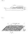
- Fig. 3 is a view illustrating the liquid crystal display device in accordance with Embodiment 1 of the present invention.
- the liquid crystal display device 1 includes an active matrix liquid crystal display panel (display panel) 2.
- the liquid crystal display panel 2 includes an active matrix substrate 10A, a counter substrate 30, and a liquid crystal layer (not illustrated) via which the active matrix substrate 10A is combined with the counter substrate 30 (see Fig. 3 ).
- the active matrix substrate 10A includes pixel electrodes (not illustrated) arranged in a matrix manner, and has (i) a display region where an image to be viewed by a viewer is displayed and (ii) a non-display region which is provided outside of the display region and in which a viewer views no image.
- a scanning line terminal section 41 is provided so that external signals are supplied to a plurality of scanning lines 12 via the scanning line terminal section 41 and
- a signal line terminal section 42 is provided so that external signals are supplied to a plurality of signal lines via the signal line terminal section 42.
- the scanning line terminal section 41 is connected to the plurality of scanning lines 12 via respective terminal lines 43.
- the signal line terminal section 42 is connected to the plurality of signal lines directly via respective terminal lines 43.
- the plurality of scanning lines 12 intersect with the plurality of signal lines, and thin film transistors (hereinafter referred to as "TFTs") 25, each of which constitutes a pixel section, are provided in the vicinity of respective intersections of the plurality of scanning lines 12 and the plurality of signal lines.
- TFTs thin film transistors
- a signal electrode (electrode) 16 a drain electrode (electrode) 17, and a pixel electrode 20 are provided. Note that a structure of a TFT 25 will be described later.
- Fig. 1 is a cross-sectional view partially illustrating the active matrix substrate in accordance with Embodiment 1 of the present invention. Note that Fig. 1 illustrates only part of the TFT 25 and its surrounding in the active matrix substrate 10A.
- the active matrix substrate 10A includes the TFTs 25 in each of which a glass 11, a scanning line 12, an insulating layer 13, a semiconductor layer 14, a signal electrode 16, a drain electrode 17, a protective layer 18, an interlayer insulating layer 19, and a pixel electrode 20 are stacked as illustrated in Fig. 1 .
- Each of the TFTs 25 has an inversely staggered (bottom gate) structure. That is, each of the TFTs 25 has a structure in which (i) the scanning line 12 is provided in a lowest layer, (ii) the insulating layer 13 and the semiconductor layer 14 are stacked on the scanning line 12 and (iii) the signal electrode 16 and the drain electrode 17 are provided on the insulating layer 13 and the semiconductor layer 14.
- the semiconductor layer 14 is constituted by a channel layer 14a and an electrode contact layer 14b.
- the semiconductor layer 14 is provided for electrically connecting the signal electrode 16 and the drain electrode 17 to each other.
- the channel layer 14a can be made from a material such as amorphous silicon.
- the channel layer 14a can be made from an oxide semiconductor of, for example, (i) zinc oxide (ZnO) or (ii) an amorphous thin film having a composition of indium oxide, gallium oxide and zinc oxide (IGZO).
- the electrode contact layer 14b can be a layer such as an N + contact layer which is doped with high concentration n-type impurities, and therefore can be made from a material such as N + amorphous silicon.
- the signal electrode 16 is provided for a signal line.
- the signal electrode 16 includes a lower signal electrode (first metal layer) 16a and an upper signal electrode (second metal layer) 16b, and is electrically connected to the semiconductor layer 14.
- the drain electrode 17 includes a lower drain electrode (first metal layer) 17a and an upper drain electrode (second metal layer) 17b, and is electrically connected to the signal electrode 16 via the semiconductor layer 14.
- a material for the lower signal electrode 16a and the lower drain electrode 17a is not limited to a specific one. It is, however, preferable that the material is a metal which is unlikely to spread during production. Examples of the metal encompass titanium (Ti), tantalum (Ta), molybdenum (Mo), and alloys thereof.
- the lower signal electrode 16a and the lower drain electrode 17a, each of which is made of the metal, do not spread onto the semiconductor layer 14. It is therefore possible to form TFTs having a favorable property.
- a material for the upper signal electrode 16b and the upper drain electrode 17b is not limited to a specific one.
- the material encompass copper (Cu), a copper alloy, and aluminum (Al).
- the material is particularly copper or the copper alloy because copper and the copper alloy have low resistances. This allows the signal electrode 16 and the drain electrode 17 to have low resistances.
- An Example of the copper is pure copper.
- Examples of the copper alloy encompass an alloy of copper and magnesium (CuMg), an alloy of copper and manganese (CuMn), an alloy of copper and aluminum (CuAl), an alloy of copper and titanium (CuTi), an alloy of copper and zirconium (CuZr), and an alloy of copper and molybdenum (CuMo).
- the scanning line 12 includes a lower scanning line 12a and an upper scanning line 12b which are not illustrated in Fig. 1 .
- the lower scanning line 12a can be made from the material for the lower signal electrode 16a and the lower drain electrode 17a.
- the upper scanning line 12b can be made from a metallic material for the upper signal electrode 16b and the upper drain electrode 17b.
- the insulating layer can be made from a material such as silicon nitride (SiNx) or silicon dioxide (SiO 2 ).
- the insulating layer 13 can be a double layer in which a layer of SiNx and a layer of SiO 2 are stacked.
- a gate insulating film 103 preferably has a thickness which falls within a range from 1000 ⁇ to 5000 ⁇ .
- the protective layer 18 can be made from a material such as silicon nitride (SiNx) or silicon dioxide (SiO 2 ).
- the interlayer insulating layer 19 is preferably made from a photosensitive material, and therefore can be made from a resin such as a photosensitive acrylic resin.
- the pixel electrode 20 can be made from a transparent conductive material such as indium tin oxide (ITO) or indium zinc oxide (IZO).
- ITO indium tin oxide
- IZO indium zinc oxide
- Fig. 2 is a cross-sectional view illustrating a main part of the active matrix substrate in accordance with Embodiment 1 of the present invention. Note here that the structure of only the drain electrode 17 will be described below, and the signal electrode 16 is identical in structure to the drain electrode 17.
- the drain electrode 17, the lower drain electrode 17a, and the upper drain electrode 17b can be read as the signal electrode 16, the lower signal electrode 16a, and the upper signal electrode 16b, respectively, as appropriate.
- Each of the TFTs 25 is configured so that (i) the lower drain electrode 17a of the drain electrode 17 is stacked on the semiconductor layer 14 so as to partially cover an upper surface of the semiconductor layer 14, specifically, in Fig. 2 , so as to partially cover an upper surface of the electrode contact layer 14b of the semiconductor layer 14, (ii) the upper drain electrode 17b is stacked on the lower drain electrode 17a and (iii) the channel layer 14a, the electrode contact layer 14b, the lower drain electrode 17a, and the upper drain electrode 17b are stacked so as to form steps.
- the lower drain electrode 17a projects farther than the upper drain electrode 17b toward a part 14aa and a part 14ba of the upper surface of the semiconductor layer 14, which parts 14aa and 14ba are not covered by the lower drain electrode 17a, so that the lower drain electrode 17a has a part 17aa which is not covered by the upper drain electrode 17b.
- a distance A between a periphery of the lower drain electrode 17a and a periphery of the upper drain electrode 17b is more than 0.4 ⁇ m but less than 1.5 ⁇ m.
- the "periphery of the lower drain electrode 17a” indicates a part where an upper surface of the lower drain electrode 17a or an end surface continuous with the upper surface of the lower drain electrode 17a is in contact with the upper surface of the semiconductor layer 14 and (ii) the "periphery of the upper drain electrode 17b” indicates a part where an upper surface of the upper drain electrode 17b or an end surface continuous with the upper surface of the upper drain electrode 17b is in contact with the upper surface of the lower drain electrode 17a.
- Fig. 12 is a view for explaining the method for producing the active matrix substrate in accordance with Embodiment 1 of the present invention.
- Fig. 12 particularly illustrates a cross-sectional structure of the active matrix substrate in which the drain electrode 17 has been patterned.
- the upper drain electrode 17b and the semiconductor layer 14 are sufficiently separated from each other in the active matrix substrate 10A of Embodiment 1. It is therefore possible to prevent the material for the upper drain electrode 17b from being moved onto the semiconductor layer 14 due to patterning of the drain electrode 17.
- Embodiment 1 even in a case where the material for the upper drain electrode 17b is any kind of metal, it is possible to prevent the metal from moving onto the semiconductor layer 14 during production. This ultimately makes it possible to prevent a TFT property from deteriorating and to keep the TFT property stable. In other words, according to Embodiment 1, it is possible to employ any kind of metal as the material for the upper drain electrode 17b without deteriorating the TFT property.
- Embodiment 1 since the distance A is less than 1.5 ⁇ m, it is possible to (i) prevent a resist from peeling off in a case where the resist is used to carry out patterning of the drain electrode 17 and (ii) easily form a wire even if the wire is thin. That is, according to a wiring structure of Embodiment 1, TFTs having a stable property can be easily formed.
- the lower drain electrode 17a can be stacked on the semiconductor layer 14 so as to completely cover the electrode contact layer 14b.
- the lower drain electrode 17a and the electrode contact layer 14b are stacked so as to partially cover an upper surface of the channel layer 14a and
- the channel layer 14a, the lower drain electrode 17a, and the upper drain electrode 17b are stacked so as to form steps.
- the electrode contact layer 14b can completely cover the channel layer 14a.
- the lower drain electrode 17a is stacked on the semiconductor layer 14 so as to partially cover the upper surface of the electrode contact layer 14b and (ii) the electrode contact layer 14b, the lower drain electrode 17a, and the upper drain electrode 17b are stacked so as to form steps.
- the active matrix substrate of Embodiment 1 is suitably applicable to a display panel of a display device.
- Embodiment 1 a process of producing the active matrix substrate 10A of Embodiment 1 will be described below. Note that the process will be described in Embodiment 1 where (i) the lower scanning line 12a, the lower signal electrode 16a and the lower drain electrode 17a are made of Ti and (ii) the upper scanning line 12b, the upper signal electrode 16b, and the upper drain electrode 17b are made of Cu.
- the active matrix substrate 10A of Embodiment 1 is produced through five photolithography steps.
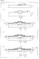
- FIG. 4 are views for explaining the method for producing the active matrix substrate in accordance with Embodiment 1 of the present invention.
- Each of (a) through (e) of Fig. 4 illustrates a cross-sectional structure obtained in a case where a corresponding one of the steps (1) through (5) has been carried out.
- each of (a) through (e) of Fig. 4 illustrates only part of a TFT 25 and its surrounding of the active matrix substrate 10A. Therefore, what will be described below is a process of producing the TFT 25 and its surrounding.
- a scanning line 12 is formed as illustrated in (a) of Fig. 4 .
- a film of Ti and a film of Cu are consecutively formed on a glass 11 by use of a sputtering method as a lower scanning line 12a and an upper scanning line 12b, respectively.
- a pattern of a resist is formed by means of photolithography.
- the lower scanning line 12a and the upper scanning line 12b are patterned by use of a wet etching method (later described).
- the resist is washed out so as to be removed.
- neither a thickness of the film of Ti nor a thickness of the film of Cu is limited to specific ones. It is, however, preferable that (i) the thickness of the film of Ti falls within a range from 30 nm to 150 nm and (ii) the thickness of the film of Cu falls within a range from 200 nm to 500 nm.
- an insulating layer 13, a channel layer 14a, and an electrode contact layer 14b are formed as illustrated in (b) of Fig. 4 .
- a film of silicon nitride, a film of amorphous silicon, and a film of n+ amorphous silicon are consecutively formed by means of CVD as the insulating layer 13, the channel layer 14a, and the electrode contact layer 14b, respectively.
- a pattern of a resist is formed by means of photolithography.
- the channel layer 14a and the electrode contact layer 14b are patterned by means of dry etching.
- the resist is washed out so as to be removed.
- thicknesses of the insulating layer 13, the channel layer 14a, and the electrode contact layer 14b are not limited to specific ones. It is, however, preferable that (i) the thickness of the insulating layer 13 made from silicon nitride falls within a range from 200 nm to 500 nm, (ii) the thickness of the channel layer 14a made from amorphous silicon falls within a range from 30 nm to 300 nm and (iii) the thickness of the electrode contact layer 14b made from n + amorphous silicon falls within a range from 50 nm to 150 nm.
- a signal electrode 16 and a drain electrode 17 are formed as illustrated in (c) of Fig. 4 .
- the signal electrode 16 and the drain electrode 18 are formed by carrying out patterning of a same film in a same layer.
- a film of Ti which serves as a lower signal electrode 16a and a lower drain electrode 17a
- a film of Cu which serves as an upper signal electrode 16b and an upper drain electrode 17b
- a pattern of a resist is formed by means of photolithography.
- the lower signal electrode 16a, the upper signal electrode 16b, the lower drain electrode 17a, and the upper drain electrode 17b are formed by carrying out patterning by use of a wet etching method (later described).
- the electrode contact layer 14b is partially removed by means of dry etching.
- the resist is washed out so as to be removed.
- neither a thickness of the film of Ti nor a thickness of the film of Cu is limited to specific ones. It is, however, preferable that (i) the thickness of the film of Ti falls within a range from 30 nm to 150 nm and (ii) the thickness of the film of Cu falls within a range from 100 nm to 400 nm.
- a protective layer 18 and an interlayer insulating layer 19 are formed as illustrated in (d) of Fig. 4 .
- a film of silicon nitride is formed as the protective layer 18 by means of CVD.
- a film of a photosensitive interlayer insulating film material is formed as the interlayer insulating layer 19.
- the film of silicon nitride and the film of the photosensitive interlayer insulating film material are subjected to photolithography and dry etching so that the protective layer 18 and the interlayer insulating layer 19 are patterned.
- a thickness of the film of silicon nitride to be formed as the protective layer 18 is not limited to a specific one. It is, however, preferable that the thickness of the film of silicon nitride falls within a range from 100 nm to 700 nm.
- a pixel electrode 20 is formed as illustrated in (e) of Fig. 4 .
- a film of a transparent conductive material such as indium tin oxide (ITO) or indium zinc oxide (IZO) is formed as the pixel electrode 20 by use of a sputtering method.
- a pattern of a resist is formed by means of photolithography.
- the pixel electrode 20 is patterned by means of wet etching.
- the resist is washed out so as to be removed.
- a thickness of the film of the transparent conductive material to be formed as the pixel electrode 20 is not limited to a specific one. It is, however, preferable that the thickness of the film of the transparent conductive material falls within a range from 50 nm to 200 nm.
- the active matrix substrate 10A is thus produced through the first to fifth steps. Note, however, that the present invention is not necessarily limited to the above-described materials and layer thicknesses, but the active matrix substrate 10A can be made from conventionally and generally used materials for an active matrix substrate.
- Each of the scanning line 12, the signal electrode 16, and the drain electrode 17 in the TFT 25 of Embodiment 1 has a two-layer structure of a lower layer and an upper layer which are stacked so as to form steps (see (e) of Fig. 4 ).
- the two-layer structures are built by carrying out the wet etching methods in the respective first and third steps in the following manner.
- the wet etching method in the first step is carried out through the following steps (1) through (3) so as to pattern the scanning line 12.
- the etchant contains (i) H 2 O 2 whose concentration is not less than 5% but is less than 20% and (ii) a fluorine compound whose concentration is not less than 0.5% but is less than 3%.
- H 2 O 2 whose concentration is not less than 5% but is less than 20%
- fluorine compound whose concentration is not less than 0.5% but is less than 3%.
- the etchant employed in Embodiment 1 is not limited to a specific one but preferably contains H 2 O 2 and a fluorine compound. This is because in a case where the etchant contains H 2 O 2 and a fluorine compound, (i) the shift amount of the film of Cu can be adjusted by changing the concentration of the H 2 O 2 contained in the etchant and (ii) the shift amount of the film of Ti can be adjusted by changing the concentration of the fluorine compound contained in the etchant. It is therefore preferable that the concentration of the H 2 O 2 contained in the etchant and the concentration of the fluorine compound contained in the etchant are adjusted as appropriate according to desired shift amounts of the film of Cu and the film of Ti.
- the wet etching method in the third step is carried out through the above-described steps (1) through (3) so as to pattern the signal electrode 16 and the drain electrode 17.
- an etchant used in the step (2) in the third step contains (i) H 2 O 2 whose concentration is not less than 5% but is less than 20% and (ii) a fluorine compound whose concentration is not less than 0.5% but is less than 3%, and it is also preferable that an etching time is 1.3 to 3 times as long as a just etching time.
- the "just etching time” means a time which is required for an upper layer (the film of Cu in the third step) of each of the signal electrode 16 and the drain electrode 17 to be etched to have a width equal to that of a resist 50.
- the wet etching method in the third step allows each of the signal electrode 16 and the drain electrode 17 to have a distance A of more than 0.4 ⁇ m but less than 1.5 ⁇ m between a periphery of a lower layer and a periphery of the upper layer.
- FIG. 5 are views for explaining a method for producing the counter substrate in accordance with Embodiment 1 of the present invention.
- Each of (a) through (c) of Fig. 5 illustrates a cross-sectional structure obtained in a case where a corresponding step has been carried out.
- the counter substrate 30 is produced through the following three photolithography steps (1) through (3).
- the active matrix substrate 10A and the counter substrate 30 are combined with each other so that a liquid crystal layer is formed between the active matrix substrate 10A and the counter substrate 30.
- a combining process will be described in the following (1) through (3).
- the liquid crystal display device 1 of Embodiment 1 is produced in which the active matrix substrate 10A is combined with the counter substrate 30 via the liquid crystal layer.
- the active matrix substrate and the display panel in accordance with Embodiment 1 of the present invention are not limitedly applied to the above described liquid crystal display device but can be applied to display devices such as an organic EL display device, an inorganic EL display device, and an electrophoretic display device. It is therefore possible to easily produce a high quality display device by providing, in the display device, an active matrix substrate in which TFTs, which have a stable property, can be easily formed.
- Embodiment 2 of the liquid crystal display device of the present invention will discuss Embodiment 2 of the liquid crystal display device of the present invention.
- Embodiment 2 is identical to Embodiment 1 except for a process of producing an active matrix substrate 10A. Therefore, Embodiment 2 will describe only a difference from Embodiment 1. Identical reference numerals are given to members having respective configurations identical to those of Embodiment 1, and descriptions of the members are omitted in Embodiment 2.
- a signal electrode 16 and a drain electrode 17 are patterned by use of a wet etching method and a dry etching method in a step which corresponds to the third step of the process of producing the active matrix substrate 10A of Embodiment 1. Except for this, Embodiment 2 employs processes identical with those in Embodiment 1.
- the signal electrode 16, the drain electrode 17, and a scanning line 12 of Embodiment 2 are patterned by use of the following methods.
- a wet etching method carried out in a first step of Embodiment 2 will be described with reference to (a) through (c) of Fig. 6 .
- the wet etching method is carried out through the following steps (1) through (3) so as to pattern the scanning line 12.
- the etchant contains (i) H 2 O 2 whose concentration is not less than 5% but is less than 20% and (ii) a fluorine compound whose concentration is not less than 0.5% but is less than 3%.
- H 2 O 2 whose concentration is not less than 5% but is less than 20%
- fluorine compound whose concentration is not less than 0.5% but is less than 3%.
- the etchant employed in Embodiment 2 is not limited to a specific one but preferably contains H 2 O 2 and a fluorine compound. This is because in a case where the etchant contains H 2 O 2 and a fluorine compound, (i) the shift amount of the film of Cu can be adjusted by changing the concentration of the H 2 O 2 contained in the etchant and (ii) the shift amount of the film of Ti can be adjusted by changing the concentration of the fluorine compound contained in the etchant. It is therefore preferable that the concentration of the H 2 O 2 contained in the etchant and the concentration of the fluorine compound contained in the etchant are adjusted as appropriate according to desired shift amounts of the film of Cu and the film of Ti.
- FIG. 7 are views for explaining a method for producing an active matrix substrate in accordance with Embodiment 2 of the present invention.
- FIG. 7 are cross-sectional views particularly illustrating respective steps which are carried out for patterning the signal electrode 16. Each of the signal electrode 16 and the drain electrode 17 is patterned through the steps.
- the wet etching method and the dry etching method are carried out through the following steps (4) through (7) so as to pattern the signal electrode 16 and the drain electrode 17.
- Embodiment 2 (i) the film of Cu is etched so as to have a width smaller than that of the resist 50 because the resist 50 is not etched by the wet etching method and then (ii) the film of Ti is etched by the dry etching method so as to have the width equal to that of the resist 50. It is therefore possible to increase a difference in shift amount between the film of Cu and the film of Ti. Note that a wet etching time of Embodiment 2 is not limited to a specific one but is preferably adjusted as appropriate according to a desired difference in shift amount between the film of Cu and the film of Ti.
- Embodiment 2 thus allows the lower signal electrode 16a and the upper signal electrode 16b to be stacked to form steps by causing the shift amount of the film of Cu to be larger than that of the film of Ti.
- the etchant used in the wet etching method and (ii) the wet etching time are adjusted so that a distance A between a periphery of a lower layer and a periphery of an upper layer of each of the signal electrode 16 and the drain electrode 17 is more than 0.4 ⁇ m but less than 1.5 ⁇ m.
- the upper layer is preferably etched (i) with use of an etchant which contains H 2 O 2 whose concentration is not less than 5% but is less than 10% and (ii) for a time that is twice to four times as long as the just etching time. This allows the distance A to be more than 0.4 ⁇ m but less than 1.5 ⁇ m.
- Embodiment 3 of the liquid crystal display device of the present invention will discuss Embodiment 3 of the liquid crystal display device of the present invention.
- Embodiment 3 is identical to Embodiments 1 and 2 except that no interlayer insulating layer 19 is provided in an active matrix substrate 10B of Embodiment 3. Therefore, Embodiment 3 will describe only a difference from Embodiments 1 and 2. Identical reference numerals are given to members having respective configurations identical to those of Embodiments 1 and 2, and descriptions of the members are omitted in Embodiment 3.
- FIG. 8 A process of producing the active matrix substrate 10B of Embodiment 3 will be described in order of the following steps (1) through (5), with reference to (a) through (e) of Fig. 8.
- FIG. 8 are views for explaining a method for producing the active matrix substrate in accordance with Embodiment 3 of the present invention.
- Each of (a) through (e) of Fig. 8 illustrates a cross-sectional structure obtained in a case where a corresponding one of the steps (1) through (5) has been carried out.
- each of (a) through (e) of Fig. 8 illustrates only part of a TFT 25 and its surrounding of the active matrix substrate 10A. Therefore, what will be described below is a process of producing the TFT 25 and its surrounding.
- a scanning line 12 is formed (see (a) of Fig. 8 ) in the same manner as the first step of Embodiment 1 or 2.
- an insulating layer 13, a channel layer 14a, and an electrode contact layer 14b are formed (see (b) of Fig. 8 ) in the same manner as the second step of Embodiment 1 or 2.
- a signal electrode 16 and a drain electrode 17 are formed (see (c) of Fig. 8 ) in the same manner as the third step of Embodiment 1 or 2.
- a protective layer 18 is formed (see (d) of Fig. 8 ).
- a film of silicon nitride is formed as the protective layer 18 by means of CVD.
- a pattern of a resist is formed by means of photolithography.
- the protective layer 18 is patterned by means of dry etching.
- the resist is washed out so as to be removed.
- a thickness of the film of silicon nitride to be formed as the protective layer 18 is not limited to a specific one but preferably falls within a range from 100 nm to 700 nm.
- a pixel electrode 20 is formed (see (e) of Fig. 8 ) in the same manner as the fifth step of Embodiment 1 or 2.
- the active matrix substrate 10B is thus produced through the above-described first to fifth steps.
- Embodiment 4 of the liquid crystal display device of the present invention will discuss Embodiment 4 of the liquid crystal display device of the present invention.
- Embodiment 4 is identical to Embodiments 1 and 2 except that a channel protective layer 21 is provided in an active matrix substrate 10C of Embodiment 4. Therefore, Embodiment 4 will describe only a difference from Embodiments 1 and 2. Identical reference numerals are given to members having respective configurations identical to those of Embodiments 1 and 2, and descriptions of the members are omitted in Embodiment 4.
- FIG. 9 A process of producing the active matrix substrate 10C of Embodiment 4 will be described in order of the following steps (1) through (5), with reference to (a) through (f) of Fig.9.
- FIG. 9 are views for explaining a method for producing the active matrix substrate in accordance with Embodiment 4 of the present invention.
- Each of (a) through (f) of Fig. 9 illustrates a cross-sectional structure obtained in a case where a corresponding one of the steps (1) through (5) has been carried out.
- each of (a) through (f) of Fig. 9 illustrates only part of a TFT 25 and its surrounding of the active matrix substrate 10C. Therefore, what will be described below is a process of producing the TFT 25 and its surrounding.
- a scanning line 12 is formed (see (a) of Fig. 9 ) in the same manner as the first step of Embodiment 1 or 2.
- an insulating layer 13, a channel layer 14a, and a channel protective layer 21 are formed (see (b) of Fig. 9 ).
- a film of silicon nitride, a film of amorphous silicon, and a film of silicon nitride are consecutively formed by means of CVD as the insulating layer 13, the channel layer 14a, and the channel protective layer 21, respectively.
- a pattern of a resist is formed by means of photolithography.
- the channel protective layer 21 is patterned by means of dry etching.
- the resist is washed out so as to be removed.
- thicknesses of the insulating layer 13, the channel layer 14a and the channel protective layer 21 are not limited to specific ones. It is, however, preferable that (i) the thickness of the insulating layer 13 made from silicon nitride falls within a range from 200 nm to 500 nm, (ii) the thickness of the channel layer 14a made from amorphous silicon falls within a range from 30 nm to 300 nm and (iii) the thickness of the channel protective layer 21 made from silicon nitride falls within a range from 100 nm to 300 nm.
- an electrode contact layer 14b, a signal electrode 16, and a drain electrode 17 are formed.
- the signal electrode 16 and the drain electrode 17 are formed by carrying out patterning of a same film in a same layer.
- a film of n+ amorphous silicon is formed as the electrode contact layer 14b by means of CVD (see (c) of Fig. 9 ). Then, (i) a film of Ti, which serves as a lower signal electrode 16a and a lower drain electrode 17a, and (ii) a film of Cu, which serves as an upper signal electrode 16b and an upper drain electrode 17b, are consecutively formed by use of a sputtering method (see (d) of Fig. 9 ). Then, a pattern of a resist is formed by means of photolithography.
- the lower signal electrode 16a, the upper signal electrode 16b, the lower drain electrode 17a, and the upper drain electrode 17b are formed by carrying out patterning by use of a method that is described in Embodiment 1 or 2. Further, the electrode contact layer 14b on the channel protective layer 21 is partially removed by means of dry etching. Lastly, the resist is washed out so as to be removed.
- thicknesses of the electrode contact layer 14b, the film of Ti and the film of Cu are not limited to specific ones. It is, however, preferable that (i) the thickness of the electrode contact layer 14b made from n + amorphous silicon falls within a range from 50 nm to 150 nm, (ii) the thickness of the film of Ti falls within a range from 30 nm to 150 nm and (iii) the thickness of the film of Cu falls within a range from 100 nm to 400 nm.
- a protective layer 18 and an interlayer insulating layer 19 are formed (see (e) of Fig. 9 ) in the same manner as the fourth step of Embodiment 1 or 2.
- a pixel electrode 20 is formed (see (f) of Fig. 9 ) in the same manner as the fifth step of Embodiment 1 or 2.
- the active matrix substrate 10C is thus produced through the above-described first to fifth steps.
- Embodiment 5 of the liquid crystal display device of the present invention will discuss Embodiment 5 of the liquid crystal display device of the present invention.
- Embodiment 5 is identical to Embodiments 1 and 2 except that an active matrix substrate 10D of Embodiment 5 includes a black matrix 22 and a color filter 23 between a protective layer 18 and an interlayer insulating layer 19 but a counter substrate of Embodiment 5 includes no layer of a black matrix 32 and a color filter 33. Therefore, Embodiment 5 will describe only a difference from Embodiments 1 and 2. Identical reference numerals are given to members having respective configurations identical to those of Embodiments 1 and 2, and descriptions of the members are omitted in Embodiment 5.
- FIG. 10 A process of producing the active matrix substrate 10D of Embodiment 5 will be described in order of the following steps (1) through (6), with reference to (a) through (f) of Fig.10.
- FIG. 10 are views for explaining a method for producing the active matrix substrate in accordance with Embodiment 5 of the present invention.
- Each of (a) through (f) of Fig. 10 illustrates a cross-sectional structure obtained in a case where a corresponding one of the steps (1) through (6) has been carried out.
- each of (a) through (f) of Fig. 10 illustrates only part of a TFT 25 and its surrounding of the active matrix substrate 10D. Therefore, what will be described below is a process of producing the TFT 25 and its surrounding.
- a protective layer 18, a black matrix 22, and a color filter 23 are formed (see (d) of Fig. 10 ).
- a film of silicon nitride is formed as the protective layer 18 by means of CVD.
- the black matrix 22, and a red, green or blue color filter 23 are formed with use of photosensitive materials by means of photolithography.
- a thickness of the film of silicon nitride to be formed as the protective layer 18 is not limited to a specific one but preferably falls within a range from 100 nm to 700 nm.
- an interlayer insulating layer 19 is formed (see (e) of Fig. 10 ). Specifically, a film of a photosensitive interlayer insulating film material is formed as the interlayer insulating layer 19, and then subjected to photolithography and dry etching so that the interlayer insulating layer 19 is patterned.
- a pixel electrode 20 is formed (see (f) of Fig. 10 ).
- a film of a transparent conductive material such as ITO (or IZO) is formed as the pixel electrode 20 by use of a sputtering method.
- a pattern of a resist is formed by means of photolithography.
- the pixel electrode 20 is patterned by means of wet etching.
- the resist is washed out so as to be removed.
- a thickness of the film of the transparent conductive material to be formed as the pixel electrode 20 is not limited to a specific one but preferably falls within a range from 50 nm to 200 nm.
- the active matrix substrate 10D is thus produced through the above-described first to sixth steps.
- the counter substrate since the active matrix substrate 10D includes the black matrix 22 and the color filter 23, the counter substrate does not need to include any layer of a black matrix and a color filter. Therefore, the counter substrate of Embodiment 5 includes neither a black matrix nor a color filter (not illustrated).
- Active matrix substrates each of which included TFTs which were identical in structure to the TFT illustrated in Fig. 1 , were prepared, and the property of the TFTs was measured. Note that the active matrix substrates were prepared by use of the method described in Embodiment 2. That is, in a third step of Example 1, patterning of a signal electrode 16 and a drain electrode 17 was carried out by use of a wet etching method and a dry etching method.
- the wet etching method was carried out under different first through third conditions so that respective first through third active matrix substrates were prepared. Under the different first through third conditions, the wet etching method was carried out for respective wet etching times of 1.5 times, 1.75 times and twice as long as a just etching time with use of an etchant having an appropriate H 2 O 2 concentration. In a case where the wet etching time was 1.5 times as long as the just etching time, a distance A was 0.2 ⁇ m between a periphery of a lower layer and a periphery of an upper layer of each of the signal electrode 16 and the drain electrode 17 of each TFT in the first active matrix substrate.
- a distance A was 0.3 ⁇ m between a periphery of a lower layer and a periphery of an upper layer of each of the signal electrode 16 and the drain electrode 17 of each TFT in the second active matrix substrate.
- each of the signal electrode 16 and the drain electrode 17a distance A was 0.45 ⁇ m between a periphery of a lower layer and a periphery of an upper layer of each of the signal electrode 16 and the drain electrode 17 of each TFT in the third active matrix substrate.
- the property of the TFTs in each of the first through third active matrix substrates was analyzed by use of a manual prober and a semiconductor parameter analyzer (that is manufactured by Agilent Technologies).
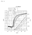
- Fig. 11 illustrates the result of the analysis.
- Fig. 11 is a graph illustrating the property of the TFTs in each of the first through third active matrix substrates in accordance with Example 1 of the present invention.
- the TFTs in each of which the distance A was 0.45 ⁇ m had a favorable property.
- Active matrix substrates each of which includes TFTs which are identical in structure to the TFT illustrated in Fig. 1 , were prepared, and conditions, under which the respective active matrix substrates were prepared, were evaluated. Note that the active matrix substrates were prepared by use of a method described in Embodiment 1. That is, in a third step of Example 2, patterning of a signal electrode 16 and a drain electrode 17 was carried out only by use of a wet etching method.
- the wet etching method was carried out under different first through third conditions so that respective first through third active matrix substrates were prepared.
- the wet etching method was carried out with use of respective first through third etchants having different H 2 O 2 concentrations.
- a distance A was 1.0 ⁇ m between a periphery of a lower layer and a periphery of an upper layer of each of the signal electrode 16 and the drain electrode 17 of each TFT in the first active matrix substrate.
- a distance A was 1.3 ⁇ m between a periphery of a lower layer and a periphery of an upper layer of each of the signal electrode 16 and the drain electrode 17 of each TFT in the second active matrix substrate.
- a distance A was 1.6 ⁇ m between a periphery of a lower layer and a periphery of an upper layer of each of the signal electrode 16 and the drain electrode 17 of each TFT in the third active matrix substrate.
- a cross-sectional shape of the drain electrode 17 and a resist 50 (photoresist) in each of the first through third active matrix substrates where wet etching of the third step has been carried out was observed through an electronic microscope.
- (a) through (c) of Fig. 15 illustrate the result of the observation.
- the resist 50 was stably left in both (i) the first active matrix substrate in which the distance A was 1.0 ⁇ m (see (a) of Fig. 15 ) and (ii) the second active matrix substrate in which the distance A was 1.3 ⁇ m (see (b) of Fig. 15 ). Therefore, the first and second active matrix substrates were capable of being subjected to dry etching immediately after the wet etching.
- the third active matrix substrate (see (c) and (d) of Fig. 15 ) in which the distance A was 1.6 ⁇ m, however, the resist 50 was peeled off in a narrow part of the drain electrode 17. Therefore, the third active matrix substrate was not capable of being subjected to dry etching immediately after the wet etching.
- Example 2 demonstrated that in a case where the distance A was 1.0 ⁇ m or 1.3 ⁇ m, it was possible to prevent the resist 50 for use in pattering of the drain electrode 17 from peeling off. That is, Example 2 strongly suggested that in a case where the distance A is less than 1.5 ⁇ m, it is possible to (i) prevent a resist from peeling off and (ii) easily form a wire even in a case where the wire is thin.
- the active matrix substrate in accordance with an embodiment of the present invention such that the second metal layer contains copper or a copper alloy.
- the configuration it is possible to reduce the resistance of the electrode because the copper and the copper alloy are low in resistance. Further, according to the configuration, it is possible to prevent the copper or the copper alloy from moving onto the semiconductor layer during production of the active matrix substrate. This makes it possible to prevent a TFT property from deteriorating and to keep the TFT property stable.
- the active matrix substrate in accordance with an embodiment of the present invention such that the first metal layer contains at least one selected from the group consisting of titanium, tantalum, molybdenum, and alloys thereof.
- the first metal layer does not move onto the semiconductor layer during production of the active matrix substrate because titanium, tantalum, molybdenum, and alloys thereof are unlikely to spread due to, for example, dry etching. It is therefore possible to prevent the TFT property from deteriorating and to keep it stable.
- the electrode is a signal electrode or a drain electrode.
- the configuration it is possible to employ any kind of metal as a material for the second metal layer of the signal electrode or the drain electrode without deteriorating the TFT property. Further, according to the configuration, it is possible to (i) prevent a resist for use in pattering of the signal electrode or the drain electrode from peeling off and (ii) easily form the signal electrode or the drain electrode even in a case where the signal electrode or the drain electrode is thin.
- each of the thin film transistors includes two electrodes each of which is the electrode, and the two electrodes are arranged so that the step part of one of the two electrodes faces the step part of the other of the two electrodes via a part of the upper surface of the semiconductor layer, which part is not covered by the first metal layers of the respective two electrodes.
- the active matrix substrate in accordance with an embodiment of the present invention such that the one of the two electrodes is a signal electrode, and the other of the two electrodes is a drain electrode.
- the configuration it is possible to employ any kind of metal as each material for the second metal layers of the signal electrode and the drain electrode without deteriorating the TFT property. Further, according to the configuration, it is possible to (i) prevent a resist for use in pattering of the signal electrode and the drain electrode from peeling off and (ii) easily form the signal electrode and the drain electrode even in a case where the signal electrode and the drain electrode are thin.
- a display panel in accordance with an embodiment of the present invention is configured to include any one of the above-described active matrix substrates.
- a display device in accordance with an embodiment of the present invention is configured to include the display panel.
- a display panel and a display device each of which includes an active matrix substrate in which TFTs having a stable property can be easily formed.
- TFTs having a stable property can be easily formed. Therefore, the present invention is suitably applicable to a case where a high quality active matrix substrate and a liquid crystal display device are produced.
Landscapes
- Physics & Mathematics (AREA)
- Nonlinear Science (AREA)
- Engineering & Computer Science (AREA)
- Microelectronics & Electronic Packaging (AREA)
- Mathematical Physics (AREA)
- Chemical & Material Sciences (AREA)
- Crystallography & Structural Chemistry (AREA)
- General Physics & Mathematics (AREA)
- Optics & Photonics (AREA)
- Thin Film Transistor (AREA)
- Liquid Crystal (AREA)
- Electrodes Of Semiconductors (AREA)
Abstract
Description
- The present invention relates to an active matrix substrate including thin film transistors, and a display panel and a display device each of which includes the active matrix substrate.
- Recently, liquid crystal display devices have rapidly become popular because they consume less electric power and are more easily downsized than CRTs (Cathode-Ray-Tubes). Among the liquid crystal display devices, active matrix liquid crystal display devices, which respond at high speed and easily carry out multi-gradation display, have been in widespread use.
- An active matrix liquid crystal display device includes (i) an active matrix substrate in which a plurality of pixels are arranged in a matrix manner, (ii) a counter substrate provided so as to face the active matrix substrate and (iii) a liquid crystal layer which is a display medium and sandwiched between the active matrix substrate and the counter substrate. In the active matrix substrate, a plurality of scanning lines and a plurality of signal lines are provided so as to intersect with each other, and pixel sections each including a thin film transistor (TFT) are provided in the vicinity of respective parts in which the plurality of scanning lines intersect with the plurality of signal lines.
-
Patent Literature 1 describes an array substrate for use in a liquid crystal display device, which array substrate includes (i) a first ohmic contact layer and a second ohmic contact layer which are provided on an active layer so as to separate from each other by a first distance, (ii) a first barrier pattern and a second barrier pattern which are provided on the first ohmic contact layer and the second ohmic contact layer, respectively, so as to separate from each other by the first distance so that the active layer is exposed between the first barrier pattern and the second barrier pattern and (iii) a source electrode and a drain electrode which are provided on the first barrier pattern and the second barrier pattern, respectively, so as to separate from each other by a second distance that is larger than the first distance, the source electrode being connected to a corresponding data line. -
Patent Literature 1
Japanese Patent Application Publication, Tokukai, No.2008-166789 A (Publication Date: July 17, 2008 - The following description will discuss an example of a conventional active matrix substrate with reference to
Figs. 13 and14. Fig. 14 is a cross-sectional view partially illustrating the conventional active matrix substrate. Specifically,Fig. 14 illustrates only part of aTFT 325 and its surrounding of a conventionalactive matrix substrate 300. - The conventional
active matrix substrate 300 includesTFTs 325 in each of which aglass 311, ascanning line 312, aninsulating layer 313, asemiconductor layer 314, asignal electrode 316, adrain electrode 317, aprotective layer 318, aninterlayer insulating layer 319, and apixel electrode 320 are stacked as illustrated inFig. 14 . Thesemiconductor layer 314 is constituted by achannel layer 314a and anelectrode contact layer 314b. Thesignal electrode 316 includes alower signal electrode 316a and anupper signal electrode 316b. Thedrain electrode 317 includes alower drain electrode 317a and anupper drain electrode 317b. - In each of the
signal electrode 316 and thedrain electrode 317 of the conventionalactive matrix substrate 300, the upper layer is stacked on the lower layer so as to cover all over an upper surface of the lower layer (seeFig. 14 ). - Note here that a material for the
upper drain electrode 317b is possibly spread during production of theactive matrix substrate 300. Specifically, the material is possibly spread, for example, by dry etching thedrain electrode 317 or by forming theprotective layer 318 by means of CVD. Such spread of the material onto thesemiconductor layer 314 deteriorates the property of the TFT. -
Fig. 13 is a view for explaining a method for producing the conventional active matrix substrate.Fig. 13 particularly illustrates a cross-sectional structure of the conventional active matrix substrate in which thedrain electrode 317 is patterned. Theupper drain electrode 317b is close to thesemiconductor layer 314 in the conventionalactive matrix substrate 300. Therefore, the material for theupper drain electrode 317b, which is spread by, for example, dry etching, is highly likely to move onto thesemiconductor layer 314 as indicated by an arrow ofFig. 13 . - According to the conventional
active matrix substrate 300, such movement of the material for theupper drain electrode 317b onto thesemiconductor layer 314 causes a problem that the property of theTFT 325 is deteriorated.Patent Literature 1 does not describe how to solve the problem. - Paten
Literature 1 describes that (i) the source electrode and the drain electrode are patterned by wet etching and (ii) barrier patterns are formed by dry etching so that the source electrode and the drain electrode are more etched (over-etched) than the barrier patterns.Patent Literature 1, however, does not describe at all how much the source electrode and the drain electrode are over-etched. In a case where the source electrode and the drain electrode are less over-etched, a material for the source electrode and a material for the drain electrode will spread onto the semiconductor layer. In contrast, in a case where the source electrode and the drain electrode are more over-etched, a resist will peel off or it will become difficult to form a thin wire. -
Patent Literature 1 describes neither the problems nor how to solve the problems. It is therefore difficult to easily form TFTs having a stable property on the basis of a wiring structure built by a conventional technique. - The present invention was made in view of the problems of the conventional technique, and an object of the present invention is to provide an active matrix substrate having a wiring structure which allows TFTs having a stable property to be easily formed, and a display panel and a display device each of which includes the active matrix substrate.
- In order to attain the object, an active matrix substrate in accordance with an embodiment of the present invention is configured to include thin film transistors each of which includes (i) a semiconductor layer and (ii) an electrode which is electrically connected to the semiconductor layer, the electrode including (i) a first metal layer stacked on the semiconductor layer so as to partially cover an upper surface of the semiconductor layer and (ii) a second metal layer stacked on the first metal layer, the semiconductor layer, the first metal layer, and the second metal layer forming steps, and in a step part in which the steps are formed, a distance between a periphery of the first metal layer and a periphery of the second metal layer being more than 0.4 µm but less than 1.5 µm.
- According to the configuration, the first metal layer is provided, and the distance between the periphery of the first metal layer and the periphery of the second metal layer is more than 0.4 µm. It is therefore possible to sufficiently separate the semiconductor layer and the second metal layer from each other. This makes it possible to prevent a material for the second metal layer from being moved onto the semiconductor layer due to, for example, pattering of the electrode during production of the active matrix substrate.
- As such, according to the configuration, it is possible to prevent a TFT property from deteriorating, and to keep the TFT property stable. It is also possible to employ any kind of metal as the material for the second metal layer without deteriorating the TFT property.
- Further, according to the configuration, the distance between the periphery of the first metal layer and the periphery of the second metal layer is less than 1.5 µm. It is therefore possible to prevent a resist for use in pattering of the electrode from peeling off, and to easily form a wire even in a case where the wire is thin. As such, according to the present invention, it is possible to provide an active matrix substrate in which TFTs having a stable property can be easily formed.
- For a fuller understanding of the nature and advantages of the invention, reference should be made to the ensuing detailed description taken in conjunction with the accompanying drawings.
- An active matrix substrate of the present invention includes thin film transistors each of which includes (i) a semiconductor layer and (ii) an electrode which is electrically connected to the semiconductor layer, the electrode including (i) a first metal layer stacked on the semiconductor layer so as to partially cover an upper surface of the semiconductor layer and (ii) a second metal layer stacked on the first metal layer, the semiconductor layer, the first metal layer, and the second metal layer forming steps, and in a step part in which the steps are formed, (i) an upper surface of the first metal layer having a first part which is not covered by the second metal layer, which first part is made by projecting the first metal layer farther than the second metal layer toward a second part of the upper surface of the semiconductor layer, which second part is not covered by the first metal layer and (ii) a distance between a periphery of the first metal layer and a periphery of the second metal layer being more than 0.4 µm but less than 1.5 µm. It is therefore possible to provide an active matrix substrate having a wiring structure which allows TFTs having a stable property to be easily formed.
-
-
Fig. 1 is a cross-sectional view partially illustrating an active matrix substrate in accordance with an embodiment of the present invention. -
Fig. 2 is a cross-sectional view illustrating a main part of the active matrix substrate in accordance with the embodiment of the present invention. -
Fig. 3 is a view illustrating a liquid crystal display device in accordance with the embodiment of the present invention.- (a) through (e) of
Fig. 4 are views for explaining a method for producing the active matrix substrate in accordance with the embodiment of the present invention. - (a) through (c) of
Fig. 5 are views for explaining a method for producing a counter substrate in accordance with the embodiment of the present invention. - (a) through (c) of
Fig. 6 are views for explaining a method for producing an active matrix substrate in accordance with another embodiment of the present invention. - (a) through (d) of
Fig. 7 are views for explaining the method for producing the active matrix substrate in accordance with the another embodiment of the present invention. - (a) through (e) of
Fig. 8 are views for explaining a method for producing an active matrix substrate in accordance with another embodiment of the present invention. - (a) through (f) of
Fig. 9 are views for explaining a method for producing an active matrix substrate in accordance with another embodiment of the present invention. - (a) through (f) of
Fig. 10 are views for explaining a method for producing an active matrix substrate in accordance with another embodiment of the present invention.
- (a) through (e) of
-
Fig. 11 is a graph illustrating the property of TFTs of each active matrix substrate in accordance with an example of the present invention. -
Fig. 12 is a view for explaining the method for producing the active matrix substrate in accordance with the embodiment of the present invention. -
Fig. 13 is a view for explaining a method for producing a conventional active matrix substrate. -
Fig. 14 is a cross-sectional view partially illustrating the conventional active matrix substrate.- (a) through (d) of
Fig. 15 illustrate electron microscopic images of active matrix substrates in each of which wet etching of a third step has been carried out.
- (a) through (d) of
- The following description will discuss in
detail Embodiment 1 of a liquid crystal display device of the present invention. - First, a configuration of a liquid crystal display device (display device) 1 of
Embodiment 1 will be described. - The configuration of the liquid
crystal display device 1 will be described with reference toFigs. 1 through 3 . First, an overall configuration of the liquidcrystal display device 1 will be described with reference toFig. 3. Fig. 3 is a view illustrating the liquid crystal display device in accordance withEmbodiment 1 of the present invention. - The liquid
crystal display device 1 includes an active matrix liquid crystal display panel (display panel) 2. The liquidcrystal display panel 2 includes anactive matrix substrate 10A, acounter substrate 30, and a liquid crystal layer (not illustrated) via which theactive matrix substrate 10A is combined with the counter substrate 30 (seeFig. 3 ). - The
active matrix substrate 10A includes pixel electrodes (not illustrated) arranged in a matrix manner, and has (i) a display region where an image to be viewed by a viewer is displayed and (ii) a non-display region which is provided outside of the display region and in which a viewer views no image. In the non-display region, (i) a scanningline terminal section 41 is provided so that external signals are supplied to a plurality ofscanning lines 12 via the scanningline terminal section 41 and (ii) a signalline terminal section 42 is provided so that external signals are supplied to a plurality of signal lines via the signalline terminal section 42. The scanningline terminal section 41 is connected to the plurality ofscanning lines 12 via respective terminal lines 43. The signalline terminal section 42 is connected to the plurality of signal lines directly via respective terminal lines 43. - In the
active matrix substrate 10A, the plurality ofscanning lines 12 intersect with the plurality of signal lines, and thin film transistors (hereinafter referred to as "TFTs") 25, each of which constitutes a pixel section, are provided in the vicinity of respective intersections of the plurality ofscanning lines 12 and the plurality of signal lines. For each of theTFTs 25, a signal electrode (electrode) 16, a drain electrode (electrode) 17, and apixel electrode 20 are provided. Note that a structure of aTFT 25 will be described later. - A basic structure of a
TFT 25 that is provided in theactive matrix substrate 10A will be described below with reference toFig. 1. Fig. 1 is a cross-sectional view partially illustrating the active matrix substrate in accordance withEmbodiment 1 of the present invention. Note thatFig. 1 illustrates only part of theTFT 25 and its surrounding in theactive matrix substrate 10A. - The
active matrix substrate 10A includes theTFTs 25 in each of which aglass 11, ascanning line 12, an insulatinglayer 13, asemiconductor layer 14, asignal electrode 16, adrain electrode 17, aprotective layer 18, aninterlayer insulating layer 19, and apixel electrode 20 are stacked as illustrated inFig. 1 . - Each of the
TFTs 25 has an inversely staggered (bottom gate) structure. That is, each of theTFTs 25 has a structure in which (i) thescanning line 12 is provided in a lowest layer, (ii) the insulatinglayer 13 and thesemiconductor layer 14 are stacked on thescanning line 12 and (iii) thesignal electrode 16 and thedrain electrode 17 are provided on the insulatinglayer 13 and thesemiconductor layer 14. - The
semiconductor layer 14 is constituted by achannel layer 14a and anelectrode contact layer 14b. Thesemiconductor layer 14 is provided for electrically connecting thesignal electrode 16 and thedrain electrode 17 to each other. - The
channel layer 14a can be made from a material such as amorphous silicon. Alternatively, thechannel layer 14a can be made from an oxide semiconductor of, for example, (i) zinc oxide (ZnO) or (ii) an amorphous thin film having a composition of indium oxide, gallium oxide and zinc oxide (IGZO). - The
electrode contact layer 14b can be a layer such as an N+ contact layer which is doped with high concentration n-type impurities, and therefore can be made from a material such as N+ amorphous silicon. - The
signal electrode 16 is provided for a signal line. Thesignal electrode 16 includes a lower signal electrode (first metal layer) 16a and an upper signal electrode (second metal layer) 16b, and is electrically connected to thesemiconductor layer 14. - The
drain electrode 17 includes a lower drain electrode (first metal layer) 17a and an upper drain electrode (second metal layer) 17b, and is electrically connected to thesignal electrode 16 via thesemiconductor layer 14. - A material for the
lower signal electrode 16a and thelower drain electrode 17a is not limited to a specific one. It is, however, preferable that the material is a metal which is unlikely to spread during production. Examples of the metal encompass titanium (Ti), tantalum (Ta), molybdenum (Mo), and alloys thereof. Thelower signal electrode 16a and thelower drain electrode 17a, each of which is made of the metal, do not spread onto thesemiconductor layer 14. It is therefore possible to form TFTs having a favorable property. - A material for the
upper signal electrode 16b and theupper drain electrode 17b is not limited to a specific one. Examples of the material encompass copper (Cu), a copper alloy, and aluminum (Al). Among the examples, it is preferable that the material is particularly copper or the copper alloy because copper and the copper alloy have low resistances. This allows thesignal electrode 16 and thedrain electrode 17 to have low resistances. - An Example of the copper is pure copper. Examples of the copper alloy encompass an alloy of copper and magnesium (CuMg), an alloy of copper and manganese (CuMn), an alloy of copper and aluminum (CuAl), an alloy of copper and titanium (CuTi), an alloy of copper and zirconium (CuZr), and an alloy of copper and molybdenum (CuMo).
- The
scanning line 12 includes alower scanning line 12a and anupper scanning line 12b which are not illustrated inFig. 1 . Thelower scanning line 12a can be made from the material for thelower signal electrode 16a and thelower drain electrode 17a. Theupper scanning line 12b can be made from a metallic material for theupper signal electrode 16b and theupper drain electrode 17b. - The insulating layer can be made from a material such as silicon nitride (SiNx) or silicon dioxide (SiO2). Alternatively, the insulating
layer 13 can be a double layer in which a layer of SiNx and a layer of SiO2 are stacked. A gate insulating film 103 preferably has a thickness which falls within a range from 1000 Å to 5000 Å. - The
protective layer 18 can be made from a material such as silicon nitride (SiNx) or silicon dioxide (SiO2). - The interlayer insulating
layer 19 is preferably made from a photosensitive material, and therefore can be made from a resin such as a photosensitive acrylic resin. - The
pixel electrode 20 can be made from a transparent conductive material such as indium tin oxide (ITO) or indium zinc oxide (IZO). - The following description will discuss in further detail structures of the
signal electrode 16 and thedrain electrode 17 of each of theTFTs 25. - The structures of the
signal electrode 16 and thedrain electrode 17 of each of theTFTs 25 will be described with reference toFig. 2. Fig. 2 is a cross-sectional view illustrating a main part of the active matrix substrate in accordance withEmbodiment 1 of the present invention. Note here that the structure of only thedrain electrode 17 will be described below, and thesignal electrode 16 is identical in structure to thedrain electrode 17. - That is, in the following description, the
drain electrode 17, thelower drain electrode 17a, and theupper drain electrode 17b can be read as thesignal electrode 16, thelower signal electrode 16a, and theupper signal electrode 16b, respectively, as appropriate. - Each of the
TFTs 25 is configured so that (i) thelower drain electrode 17a of thedrain electrode 17 is stacked on thesemiconductor layer 14 so as to partially cover an upper surface of thesemiconductor layer 14, specifically, inFig. 2 , so as to partially cover an upper surface of theelectrode contact layer 14b of thesemiconductor layer 14, (ii) theupper drain electrode 17b is stacked on thelower drain electrode 17a and (iii) thechannel layer 14a, theelectrode contact layer 14b, thelower drain electrode 17a, and theupper drain electrode 17b are stacked so as to form steps. - In a step part where the steps are formed, the
lower drain electrode 17a projects farther than theupper drain electrode 17b toward a part 14aa and a part 14ba of the upper surface of thesemiconductor layer 14, which parts 14aa and 14ba are not covered by thelower drain electrode 17a, so that thelower drain electrode 17a has a part 17aa which is not covered by theupper drain electrode 17b. - Further, in the step part, a distance A between a periphery of the
lower drain electrode 17a and a periphery of theupper drain electrode 17b is more than 0.4 µm but less than 1.5 µm. - Note here that (i) the "periphery of the
lower drain electrode 17a" indicates a part where an upper surface of thelower drain electrode 17a or an end surface continuous with the upper surface of thelower drain electrode 17a is in contact with the upper surface of thesemiconductor layer 14 and (ii) the "periphery of theupper drain electrode 17b" indicates a part where an upper surface of theupper drain electrode 17b or an end surface continuous with the upper surface of theupper drain electrode 17b is in contact with the upper surface of thelower drain electrode 17a. - According to
Embodiment 1, since thelower drain electrode 17a is provided and the distance A is more than 0.4 µm, thesemiconductor layer 14 and theupper drain electrode 17b can be sufficiently separated from each other.Fig. 12 is a view for explaining the method for producing the active matrix substrate in accordance withEmbodiment 1 of the present invention.Fig. 12 particularly illustrates a cross-sectional structure of the active matrix substrate in which thedrain electrode 17 has been patterned. As illustrated inFig. 12 , theupper drain electrode 17b and thesemiconductor layer 14 are sufficiently separated from each other in theactive matrix substrate 10A ofEmbodiment 1. It is therefore possible to prevent the material for theupper drain electrode 17b from being moved onto thesemiconductor layer 14 due to patterning of thedrain electrode 17. - As such, according to
Embodiment 1, even in a case where the material for theupper drain electrode 17b is any kind of metal, it is possible to prevent the metal from moving onto thesemiconductor layer 14 during production. This ultimately makes it possible to prevent a TFT property from deteriorating and to keep the TFT property stable. In other words, according toEmbodiment 1, it is possible to employ any kind of metal as the material for theupper drain electrode 17b without deteriorating the TFT property. - According to
Embodiment 1, since the distance A is less than 1.5 µm, it is possible to (i) prevent a resist from peeling off in a case where the resist is used to carry out patterning of thedrain electrode 17 and (ii) easily form a wire even if the wire is thin. That is, according to a wiring structure ofEmbodiment 1, TFTs having a stable property can be easily formed. - Note that the
lower drain electrode 17a can be stacked on thesemiconductor layer 14 so as to completely cover theelectrode contact layer 14b. In this case, (i) thelower drain electrode 17a and theelectrode contact layer 14b are stacked so as to partially cover an upper surface of thechannel layer 14a and (ii) thechannel layer 14a, thelower drain electrode 17a, and theupper drain electrode 17b are stacked so as to form steps. - Alternatively, the
electrode contact layer 14b can completely cover thechannel layer 14a. In this case, (i) thelower drain electrode 17a is stacked on thesemiconductor layer 14 so as to partially cover the upper surface of theelectrode contact layer 14b and (ii) theelectrode contact layer 14b, thelower drain electrode 17a, and theupper drain electrode 17b are stacked so as to form steps. - The active matrix substrate of
Embodiment 1 is suitably applicable to a display panel of a display device. - The following description will discuss a method for producing the liquid
crystal display device 1 ofEmbodiment 1. - First, a process of producing the
active matrix substrate 10A ofEmbodiment 1 will be described below. Note that the process will be described inEmbodiment 1 where (i) thelower scanning line 12a, thelower signal electrode 16a and thelower drain electrode 17a are made of Ti and (ii) theupper scanning line 12b, theupper signal electrode 16b, and theupper drain electrode 17b are made of Cu. - The
active matrix substrate 10A ofEmbodiment 1 is produced through five photolithography steps. - The process of producing the
active matrix substrate 10A ofEmbodiment 1 will be described in order of the following steps (1) through (5), with reference to (a) through (e) ofFig. 4. (a) through (e) ofFig. 4 are views for explaining the method for producing the active matrix substrate in accordance withEmbodiment 1 of the present invention. Each of (a) through (e) ofFig. 4 illustrates a cross-sectional structure obtained in a case where a corresponding one of the steps (1) through (5) has been carried out. Specifically, each of (a) through (e) ofFig. 4 illustrates only part of aTFT 25 and its surrounding of theactive matrix substrate 10A. Therefore, what will be described below is a process of producing theTFT 25 and its surrounding. - In a first step, a
scanning line 12 is formed as illustrated in (a) ofFig. 4 . First, a film of Ti and a film of Cu are consecutively formed on aglass 11 by use of a sputtering method as alower scanning line 12a and anupper scanning line 12b, respectively. Then, a pattern of a resist is formed by means of photolithography. Subsequently, thelower scanning line 12a and theupper scanning line 12b are patterned by use of a wet etching method (later described). Lastly, the resist is washed out so as to be removed. - In the first step, neither a thickness of the film of Ti nor a thickness of the film of Cu is limited to specific ones. It is, however, preferable that (i) the thickness of the film of Ti falls within a range from 30 nm to 150 nm and (ii) the thickness of the film of Cu falls within a range from 200 nm to 500 nm.
- In a second step, an insulating
layer 13, achannel layer 14a, and anelectrode contact layer 14b are formed as illustrated in (b) ofFig. 4 . First, a film of silicon nitride, a film of amorphous silicon, and a film of n+ amorphous silicon are consecutively formed by means of CVD as the insulatinglayer 13, thechannel layer 14a, and theelectrode contact layer 14b, respectively. Then, a pattern of a resist is formed by means of photolithography. Subsequently, thechannel layer 14a and theelectrode contact layer 14b are patterned by means of dry etching. Lastly, the resist is washed out so as to be removed. - In the second step, thicknesses of the insulating
layer 13, thechannel layer 14a, and theelectrode contact layer 14b are not limited to specific ones. It is, however, preferable that (i) the thickness of the insulatinglayer 13 made from silicon nitride falls within a range from 200 nm to 500 nm, (ii) the thickness of thechannel layer 14a made from amorphous silicon falls within a range from 30 nm to 300 nm and (iii) the thickness of theelectrode contact layer 14b made from n+ amorphous silicon falls within a range from 50 nm to 150 nm. - In a third step, a
signal electrode 16 and adrain electrode 17 are formed as illustrated in (c) ofFig. 4 . Specifically, thesignal electrode 16 and thedrain electrode 18 are formed by carrying out patterning of a same film in a same layer. - First, (i) a film of Ti, which serves as a
lower signal electrode 16a and alower drain electrode 17a, and (ii) a film of Cu, which serves as anupper signal electrode 16b and anupper drain electrode 17b, are consecutively formed by use of a sputtering method. Then, a pattern of a resist is formed by means of photolithography. Subsequently, thelower signal electrode 16a, theupper signal electrode 16b, thelower drain electrode 17a, and theupper drain electrode 17b are formed by carrying out patterning by use of a wet etching method (later described). Further, theelectrode contact layer 14b is partially removed by means of dry etching. Lastly, the resist is washed out so as to be removed. - In the third step, neither a thickness of the film of Ti nor a thickness of the film of Cu is limited to specific ones. It is, however, preferable that (i) the thickness of the film of Ti falls within a range from 30 nm to 150 nm and (ii) the thickness of the film of Cu falls within a range from 100 nm to 400 nm.
- In a fourth step, a
protective layer 18 and an interlayer insulatinglayer 19 are formed as illustrated in (d) ofFig. 4 . First, a film of silicon nitride is formed as theprotective layer 18 by means of CVD. Then, a film of a photosensitive interlayer insulating film material is formed as theinterlayer insulating layer 19. Subsequently, the film of silicon nitride and the film of the photosensitive interlayer insulating film material are subjected to photolithography and dry etching so that theprotective layer 18 and the interlayer insulatinglayer 19 are patterned. - In the fourth step, a thickness of the film of silicon nitride to be formed as the
protective layer 18 is not limited to a specific one. It is, however, preferable that the thickness of the film of silicon nitride falls within a range from 100 nm to 700 nm. - In a fifth step, a
pixel electrode 20 is formed as illustrated in (e) ofFig. 4 . First, a film of a transparent conductive material such as indium tin oxide (ITO) or indium zinc oxide (IZO) is formed as thepixel electrode 20 by use of a sputtering method. Then, a pattern of a resist is formed by means of photolithography. Subsequently, thepixel electrode 20 is patterned by means of wet etching. Lastly, the resist is washed out so as to be removed. - In the fifth step, a thickness of the film of the transparent conductive material to be formed as the
pixel electrode 20 is not limited to a specific one. It is, however, preferable that the thickness of the film of the transparent conductive material falls within a range from 50 nm to 200 nm. - The
active matrix substrate 10A is thus produced through the first to fifth steps. Note, however, that the present invention is not necessarily limited to the above-described materials and layer thicknesses, but theactive matrix substrate 10A can be made from conventionally and generally used materials for an active matrix substrate. - Each of the
scanning line 12, thesignal electrode 16, and thedrain electrode 17 in theTFT 25 ofEmbodiment 1 has a two-layer structure of a lower layer and an upper layer which are stacked so as to form steps (see (e) ofFig. 4 ). - According to
Embodiment 1, the two-layer structures are built by carrying out the wet etching methods in the respective first and third steps in the following manner. - The wet etching method carried out in the first step of
Embodiment 1 will be described with reference to (a) through (c) ofFig. 6. (a) through (c) ofFig. 6 are views for explaining the method for producing the active matrix substrate in accordance withEmbodiment 1 of the present invention. (a) through (c) ofFig. 6 are cross-sectional views particularly illustrating respective steps which are carried out for patterning thescanning line 12. - The wet etching method in the first step is carried out through the following steps (1) through (3) so as to pattern the
scanning line 12. - (1) Immediately before the wet etching method is carried out in the first step, (i) the film of Ti and the film of Cu are formed and stacked in this order on the
glass 11 as thelower scanning line 12a and theupper scanning line 12b, respectively and then (ii) a resist 50 is formed by means of photolithography (see (a) ofFig. 6 ). - (2) The film of Ti and the film of Cu are simultaneously etched by the wet etching method with use of an etchant which contains hydrogen peroxide (H2O2) and a fluorine compound (see (b) of
Fig. 6 ). - It is preferable in
Embodiment 1 that the etchant contains (i) H2O2 whose concentration is not less than 5% but is less than 20% and (ii) a fluorine compound whose concentration is not less than 0.5% but is less than 3%. With use of the etchant, it is possible to etch the film of Cu faster than to etch the film of Ti. Such etching causes a shift amount (etching rate) of the film of Cu to be larger than that of the film of Ti. This allows thelower scanning line 12a and theupper scanning line 12b to be stacked to form steps (see (b) ofFig. 6 ). - Note that the etchant employed in
Embodiment 1 is not limited to a specific one but preferably contains H2O2 and a fluorine compound. This is because in a case where the etchant contains H2O2 and a fluorine compound, (i) the shift amount of the film of Cu can be adjusted by changing the concentration of the H2O2 contained in the etchant and (ii) the shift amount of the film of Ti can be adjusted by changing the concentration of the fluorine compound contained in the etchant. It is therefore preferable that the concentration of the H2O2 contained in the etchant and the concentration of the fluorine compound contained in the etchant are adjusted as appropriate according to desired shift amounts of the film of Cu and the film of Ti. - (3) The resist 50 is washed out so as to be removed. This ultimately completes a pattern of the scanning line 12 (see (c) of
Fig. 6 ). - The wet etching method in the third step is carried out through the above-described steps (1) through (3) so as to pattern the
signal electrode 16 and thedrain electrode 17. Note that it is preferable that an etchant used in the step (2) in the third step contains (i) H2O2 whose concentration is not less than 5% but is less than 20% and (ii) a fluorine compound whose concentration is not less than 0.5% but is less than 3%, and it is also preferable that an etching time is 1.3 to 3 times as long as a just etching time. Note that the "just etching time" means a time which is required for an upper layer (the film of Cu in the third step) of each of thesignal electrode 16 and thedrain electrode 17 to be etched to have a width equal to that of a resist 50. - The wet etching method in the third step allows each of the
signal electrode 16 and thedrain electrode 17 to have a distance A of more than 0.4 µm but less than 1.5 µm between a periphery of a lower layer and a periphery of the upper layer. - The following description will discuss a process of producing a
counter substrate 30 ofEmbodiment 1, with reference to (a) through (c) ofFig. 5. (a) through (c) ofFig. 5 are views for explaining a method for producing the counter substrate in accordance withEmbodiment 1 of the present invention. Each of (a) through (c) ofFig. 5 illustrates a cross-sectional structure obtained in a case where a corresponding step has been carried out. - The
counter substrate 30 is produced through the following three photolithography steps (1) through (3). - (1) A
black matrix 32, and a red, green orblue color filter 33 are formed on aglass 31 with use of photosensitive materials by means of photolithography (see (a) ofFig. 5 ). - (2) A
pixel electrode 34 of 50 nm to 200 nm in thickness is formed by use of a sputtering method, and then patterned by means of photolithography and wet etching (see (b) ofFig. 5 ). This forms a common electrode. - (3)
Photo spacers 35 are formed with use of a photosensitive material by means of photolithography (see (c) ofFig. 5 ). - The
active matrix substrate 10A and thecounter substrate 30 are combined with each other so that a liquid crystal layer is formed between theactive matrix substrate 10A and thecounter substrate 30. A combining process will be described in the following (1) through (3). - (1) First, an alignment film of polyimide is formed on each of the
active matrix substrate 10A and thecounter substrate 30 by use of a printing method. - (2) The
active matrix substrate 10A and thecounter substrate 30 are combined with each other after a sealing agent is printed and liquid crystal is dropped. - (3) The
active matrix substrate 10A and thecounter substrate 30 thus combined are diced. - Through the steps (1) through (3), the liquid
crystal display device 1 ofEmbodiment 1 is produced in which theactive matrix substrate 10A is combined with thecounter substrate 30 via the liquid crystal layer. - Note that the active matrix substrate and the display panel in accordance with
Embodiment 1 of the present invention are not limitedly applied to the above described liquid crystal display device but can be applied to display devices such as an organic EL display device, an inorganic EL display device, and an electrophoretic display device. It is therefore possible to easily produce a high quality display device by providing, in the display device, an active matrix substrate in which TFTs, which have a stable property, can be easily formed. - The following description will discuss
Embodiment 2 of the liquid crystal display device of the present invention. -
Embodiment 2 is identical toEmbodiment 1 except for a process of producing anactive matrix substrate 10A. Therefore,Embodiment 2 will describe only a difference fromEmbodiment 1. Identical reference numerals are given to members having respective configurations identical to those ofEmbodiment 1, and descriptions of the members are omitted inEmbodiment 2. - In
Embodiment 2, asignal electrode 16 and adrain electrode 17 are patterned by use of a wet etching method and a dry etching method in a step which corresponds to the third step of the process of producing theactive matrix substrate 10A ofEmbodiment 1. Except for this,Embodiment 2 employs processes identical with those inEmbodiment 1. Thesignal electrode 16, thedrain electrode 17, and ascanning line 12 ofEmbodiment 2 are patterned by use of the following methods. - First, a wet etching method carried out in a first step of
Embodiment 2 will be described with reference to (a) through (c) ofFig. 6 . In the first step, the wet etching method is carried out through the following steps (1) through (3) so as to pattern thescanning line 12. - (1) Immediately before the wet etching method is carried out in the first step, (i) a film of Ti and a film of Cu are formed and stacked in this order on a
glass 11 as alower scanning line 12a and anupper scanning line 12b, respectively and then (ii) a resist 50 is formed by means of photolithography (see (a) ofFig. 6 ). - (2) The film of Ti and the film of Cu are simultaneously etched by the wet etching method with use of an etchant which contains hydrogen peroxide (H2O2) and a fluorine compound (see (b) of
Fig. 6 ). - It is preferable in
Embodiment 2 that the etchant contains (i) H2O2 whose concentration is not less than 5% but is less than 20% and (ii) a fluorine compound whose concentration is not less than 0.5% but is less than 3%. With use of the etchant, it is possible to etch the film of Cu faster than to etch the film of Ti. Such etching causes a shift amount (etching rate) of the film of Cu to be larger than that of the film of Ti. This allows thelower scanning line 12a and theupper scanning line 12b to be stacked to form steps (see (b) ofFig. 6 ). - Note that the etchant employed in
Embodiment 2 is not limited to a specific one but preferably contains H2O2 and a fluorine compound. This is because in a case where the etchant contains H2O2 and a fluorine compound, (i) the shift amount of the film of Cu can be adjusted by changing the concentration of the H2O2 contained in the etchant and (ii) the shift amount of the film of Ti can be adjusted by changing the concentration of the fluorine compound contained in the etchant. It is therefore preferable that the concentration of the H2O2 contained in the etchant and the concentration of the fluorine compound contained in the etchant are adjusted as appropriate according to desired shift amounts of the film of Cu and the film of Ti. - (3) The resist 50 is washed out so as to be removed. This ultimately completes a pattern of the scanning line 12 (see (c) of
Fig. 6 ). - Next, a wet etching method and a dry etching method, which are carried out in a third step of
Embodiment 2, will be described with reference to (a) through (d) ofFig. 7. (a) through (d) ofFig. 7 are views for explaining a method for producing an active matrix substrate in accordance withEmbodiment 2 of the present invention. (a) through (d) ofFig. 7 are cross-sectional views particularly illustrating respective steps which are carried out for patterning thesignal electrode 16. Each of thesignal electrode 16 and thedrain electrode 17 is patterned through the steps. - In the third step, the wet etching method and the dry etching method are carried out through the following steps (4) through (7) so as to pattern the
signal electrode 16 and thedrain electrode 17. - (4) Immediately before the wet etching method and the dry etching method are carried out in the third step, (i) a film of Ti and a film of Cu are formed and stacked in this order on a base as a
lower signal electrode 16a and anupper signal electrode 16b, respectively and then (ii) a resist 50 is formed by means of photolithography (see (a) ofFig. 7 ). - (5) The film of Cu is etched by the wet etching method with use of an etchant which contains hydrogen peroxide (H2O2) (see (b) of
Fig. 7 ). - (6) The film of Ti is etched by use of the dry etching method so as to have a width equal to that of the resist 50 (see (c) of
Fig. 7 ). - (7) The resist 50 is washed out so as to be removed. This ultimately completes a pattern of the signal electrode 16 (see (d) of
Fig. 7 ). - According to
Embodiment 2, (i) the film of Cu is etched so as to have a width smaller than that of the resist 50 because the resist 50 is not etched by the wet etching method and then (ii) the film of Ti is etched by the dry etching method so as to have the width equal to that of the resist 50. It is therefore possible to increase a difference in shift amount between the film of Cu and the film of Ti. Note that a wet etching time ofEmbodiment 2 is not limited to a specific one but is preferably adjusted as appropriate according to a desired difference in shift amount between the film of Cu and the film of Ti. -
Embodiment 2 thus allows thelower signal electrode 16a and theupper signal electrode 16b to be stacked to form steps by causing the shift amount of the film of Cu to be larger than that of the film of Ti. - Note that, in the step (5) of the third step, it is preferable that (i) the etchant used in the wet etching method and (ii) the wet etching time are adjusted so that a distance A between a periphery of a lower layer and a periphery of an upper layer of each of the
signal electrode 16 and thedrain electrode 17 is more than 0.4 µm but less than 1.5 µm. For example, in a case where the upper layer is made of copper, the upper layer is preferably etched (i) with use of an etchant which contains H2O2 whose concentration is not less than 5% but is less than 10% and (ii) for a time that is twice to four times as long as the just etching time. This allows the distance A to be more than 0.4 µm but less than 1.5 µm. - The following description will discuss Embodiment 3 of the liquid crystal display device of the present invention.
- Embodiment 3 is identical to Embodiments 1 and 2 except that no
interlayer insulating layer 19 is provided in anactive matrix substrate 10B of Embodiment 3. Therefore, Embodiment 3 will describe only a difference fromEmbodiments Embodiments - A process of producing the
active matrix substrate 10B of Embodiment 3 will be described in order of the following steps (1) through (5), with reference to (a) through (e) ofFig. 8. (a) through (e) ofFig. 8 are views for explaining a method for producing the active matrix substrate in accordance with Embodiment 3 of the present invention. Each of (a) through (e) ofFig. 8 illustrates a cross-sectional structure obtained in a case where a corresponding one of the steps (1) through (5) has been carried out. Specifically, each of (a) through (e) ofFig. 8 illustrates only part of aTFT 25 and its surrounding of theactive matrix substrate 10A. Therefore, what will be described below is a process of producing theTFT 25 and its surrounding. - In a first step, a
scanning line 12 is formed (see (a) ofFig. 8 ) in the same manner as the first step ofEmbodiment - In a second step, an insulating
layer 13, achannel layer 14a, and anelectrode contact layer 14b are formed (see (b) ofFig. 8 ) in the same manner as the second step ofEmbodiment - In a third step, a
signal electrode 16 and adrain electrode 17 are formed (see (c) ofFig. 8 ) in the same manner as the third step ofEmbodiment - In a fourth step, a
protective layer 18 is formed (see (d) ofFig. 8 ). First, a film of silicon nitride is formed as theprotective layer 18 by means of CVD. Then, a pattern of a resist is formed by means of photolithography. Subsequently, theprotective layer 18 is patterned by means of dry etching. Lastly, the resist is washed out so as to be removed. - In the fourth step, a thickness of the film of silicon nitride to be formed as the
protective layer 18 is not limited to a specific one but preferably falls within a range from 100 nm to 700 nm. - In a fifth step, a
pixel electrode 20 is formed (see (e) ofFig. 8 ) in the same manner as the fifth step ofEmbodiment - The
active matrix substrate 10B is thus produced through the above-described first to fifth steps. - The following description will discuss Embodiment 4 of the liquid crystal display device of the present invention.
- Embodiment 4 is identical to Embodiments 1 and 2 except that a channel
protective layer 21 is provided in an active matrix substrate 10C of Embodiment 4. Therefore, Embodiment 4 will describe only a difference fromEmbodiments Embodiments - A process of producing the active matrix substrate 10C of Embodiment 4 will be described in order of the following steps (1) through (5), with reference to (a) through (f) of
Fig.9. (a) through (f) ofFig. 9 are views for explaining a method for producing the active matrix substrate in accordance with Embodiment 4 of the present invention. Each of (a) through (f) ofFig. 9 illustrates a cross-sectional structure obtained in a case where a corresponding one of the steps (1) through (5) has been carried out. Specifically, each of (a) through (f) ofFig. 9 illustrates only part of aTFT 25 and its surrounding of the active matrix substrate 10C. Therefore, what will be described below is a process of producing theTFT 25 and its surrounding. - In a first step, a
scanning line 12 is formed (see (a) ofFig. 9 ) in the same manner as the first step ofEmbodiment - In a second step, an insulating
layer 13, achannel layer 14a, and a channelprotective layer 21 are formed (see (b) ofFig. 9 ). First, a film of silicon nitride, a film of amorphous silicon, and a film of silicon nitride are consecutively formed by means of CVD as the insulatinglayer 13, thechannel layer 14a, and the channelprotective layer 21, respectively. Then, a pattern of a resist is formed by means of photolithography. Subsequently, the channelprotective layer 21 is patterned by means of dry etching. Lastly, the resist is washed out so as to be removed. - In the second step, thicknesses of the insulating
layer 13, thechannel layer 14a and the channelprotective layer 21 are not limited to specific ones. It is, however, preferable that (i) the thickness of the insulatinglayer 13 made from silicon nitride falls within a range from 200 nm to 500 nm, (ii) the thickness of thechannel layer 14a made from amorphous silicon falls within a range from 30 nm to 300 nm and (iii) the thickness of the channelprotective layer 21 made from silicon nitride falls within a range from 100 nm to 300 nm. - In a third step, an
electrode contact layer 14b, asignal electrode 16, and adrain electrode 17 are formed. Thesignal electrode 16 and thedrain electrode 17 are formed by carrying out patterning of a same film in a same layer. - First, a film of n+ amorphous silicon is formed as the
electrode contact layer 14b by means of CVD (see (c) ofFig. 9 ). Then, (i) a film of Ti, which serves as alower signal electrode 16a and alower drain electrode 17a, and (ii) a film of Cu, which serves as anupper signal electrode 16b and anupper drain electrode 17b, are consecutively formed by use of a sputtering method (see (d) ofFig. 9 ). Then, a pattern of a resist is formed by means of photolithography. Subsequently, thelower signal electrode 16a, theupper signal electrode 16b, thelower drain electrode 17a, and theupper drain electrode 17b are formed by carrying out patterning by use of a method that is described inEmbodiment electrode contact layer 14b on the channelprotective layer 21 is partially removed by means of dry etching. Lastly, the resist is washed out so as to be removed. - In the third step, thicknesses of the
electrode contact layer 14b, the film of Ti and the film of Cu are not limited to specific ones. It is, however, preferable that (i) the thickness of theelectrode contact layer 14b made from n+ amorphous silicon falls within a range from 50 nm to 150 nm, (ii) the thickness of the film of Ti falls within a range from 30 nm to 150 nm and (iii) the thickness of the film of Cu falls within a range from 100 nm to 400 nm. - In a fourth step, a
protective layer 18 and an interlayer insulatinglayer 19 are formed (see (e) ofFig. 9 ) in the same manner as the fourth step ofEmbodiment - In a fifth step, a
pixel electrode 20 is formed (see (f) ofFig. 9 ) in the same manner as the fifth step ofEmbodiment - The active matrix substrate 10C is thus produced through the above-described first to fifth steps.
- The following description will discuss Embodiment 5 of the liquid crystal display device of the present invention.
- Embodiment 5 is identical to Embodiments 1 and 2 except that an
active matrix substrate 10D of Embodiment 5 includes ablack matrix 22 and acolor filter 23 between aprotective layer 18 and an interlayer insulatinglayer 19 but a counter substrate of Embodiment 5 includes no layer of ablack matrix 32 and acolor filter 33. Therefore, Embodiment 5 will describe only a difference fromEmbodiments Embodiments - A process of producing the
active matrix substrate 10D of Embodiment 5 will be described in order of the following steps (1) through (6), with reference to (a) through (f) ofFig.10. (a) through (f) ofFig. 10 are views for explaining a method for producing the active matrix substrate in accordance with Embodiment 5 of the present invention. Each of (a) through (f) ofFig. 10 illustrates a cross-sectional structure obtained in a case where a corresponding one of the steps (1) through (6) has been carried out. Specifically, each of (a) through (f) ofFig. 10 illustrates only part of aTFT 25 and its surrounding of theactive matrix substrate 10D. Therefore, what will be described below is a process of producing theTFT 25 and its surrounding. - (1) First Step, (2) Second Step, and (3) Third Step of Embodiment 5 are exactly the same as those of
Embodiment Fig. 10 illustrates a cross-sectional structure obtained in a case where a corresponding one of the respective first through third steps has been carried out. - In a fourth step, a
protective layer 18, ablack matrix 22, and acolor filter 23 are formed (see (d) ofFig. 10 ). First, a film of silicon nitride is formed as theprotective layer 18 by means of CVD. Then, theblack matrix 22, and a red, green orblue color filter 23 are formed with use of photosensitive materials by means of photolithography. - In the fourth step, a thickness of the film of silicon nitride to be formed as the
protective layer 18 is not limited to a specific one but preferably falls within a range from 100 nm to 700 nm. - In a fifth step, an
interlayer insulating layer 19 is formed (see (e) ofFig. 10 ). Specifically, a film of a photosensitive interlayer insulating film material is formed as theinterlayer insulating layer 19, and then subjected to photolithography and dry etching so that the interlayer insulatinglayer 19 is patterned. - In a sixth step, a
pixel electrode 20 is formed (see (f) ofFig. 10 ). First, a film of a transparent conductive material such as ITO (or IZO) is formed as thepixel electrode 20 by use of a sputtering method. Then, a pattern of a resist is formed by means of photolithography. Subsequently, thepixel electrode 20 is patterned by means of wet etching. Lastly, the resist is washed out so as to be removed. - In the sixth step, a thickness of the film of the transparent conductive material to be formed as the
pixel electrode 20 is not limited to a specific one but preferably falls within a range from 50 nm to 200 nm. - The
active matrix substrate 10D is thus produced through the above-described first to sixth steps. - According to Embodiment 5, since the
active matrix substrate 10D includes theblack matrix 22 and thecolor filter 23, the counter substrate does not need to include any layer of a black matrix and a color filter. Therefore, the counter substrate of Embodiment 5 includes neither a black matrix nor a color filter (not illustrated). - The present invention is not limited to the description of the embodiments above, and can therefore be modified by a skilled person in the art within the scope of the claims. Namely, an embodiment derived from a proper combination of technical means disclosed in different embodiments is encompassed in the technical scope of the present invention.
- Active matrix substrates, each of which included TFTs which were identical in structure to the TFT illustrated in
Fig. 1 , were prepared, and the property of the TFTs was measured. Note that the active matrix substrates were prepared by use of the method described inEmbodiment 2. That is, in a third step of Example 1, patterning of asignal electrode 16 and adrain electrode 17 was carried out by use of a wet etching method and a dry etching method. - In the third step, the wet etching method was carried out under different first through third conditions so that respective first through third active matrix substrates were prepared. Under the different first through third conditions, the wet etching method was carried out for respective wet etching times of 1.5 times, 1.75 times and twice as long as a just etching time with use of an etchant having an appropriate H2O2 concentration. In a case where the wet etching time was 1.5 times as long as the just etching time, a distance A was 0.2 µm between a periphery of a lower layer and a periphery of an upper layer of each of the
signal electrode 16 and thedrain electrode 17 of each TFT in the first active matrix substrate. In a case where the wet etching time was 1.75 times as long as the just etching time, a distance A was 0.3 µm between a periphery of a lower layer and a periphery of an upper layer of each of thesignal electrode 16 and thedrain electrode 17 of each TFT in the second active matrix substrate. In a case where the wet etching time was twice as long as the just etching time, each of thesignal electrode 16 and thedrain electrode 17a distance A was 0.45 µm between a periphery of a lower layer and a periphery of an upper layer of each of thesignal electrode 16 and thedrain electrode 17 of each TFT in the third active matrix substrate. - The property of the TFTs in each of the first through third active matrix substrates was analyzed by use of a manual prober and a semiconductor parameter analyzer (that is manufactured by Agilent Technologies).
-
Fig. 11 illustrates the result of the analysis.Fig. 11 is a graph illustrating the property of the TFTs in each of the first through third active matrix substrates in accordance with Example 1 of the present invention. As is clear fromFig. 11 , the property of the TFTs, in each of which the distance A was not more than 0.5 µm, that is, the distance A was 0.2 µm or 0.3 µm, remarkably shifted toward a positive side. On the other hand, the TFTs in each of which the distance A was 0.45 µm had a favorable property. - Active matrix substrates, each of which includes TFTs which are identical in structure to the TFT illustrated in
Fig. 1 , were prepared, and conditions, under which the respective active matrix substrates were prepared, were evaluated. Note that the active matrix substrates were prepared by use of a method described inEmbodiment 1. That is, in a third step of Example 2, patterning of asignal electrode 16 and adrain electrode 17 was carried out only by use of a wet etching method. - In the third step, the wet etching method was carried out under different first through third conditions so that respective first through third active matrix substrates were prepared.
- Under different first through third conditions, the wet etching method was carried out with use of respective first through third etchants having different H2O2 concentrations. In a case where the first etchant was used, a distance A was 1.0 µm between a periphery of a lower layer and a periphery of an upper layer of each of the
signal electrode 16 and thedrain electrode 17 of each TFT in the first active matrix substrate. In a case where the second etchant was used, a distance A was 1.3 µm between a periphery of a lower layer and a periphery of an upper layer of each of thesignal electrode 16 and thedrain electrode 17 of each TFT in the second active matrix substrate. In a case where the third etchant was used, a distance A was 1.6 µm between a periphery of a lower layer and a periphery of an upper layer of each of thesignal electrode 16 and thedrain electrode 17 of each TFT in the third active matrix substrate. - A cross-sectional shape of the
drain electrode 17 and a resist 50 (photoresist) in each of the first through third active matrix substrates where wet etching of the third step has been carried out was observed through an electronic microscope. (a) through (c) ofFig. 15 illustrate the result of the observation. - (a) through (d) of
Fig. 15 illustrate electron microscopic images of the first through third active matrix substrates in each of which wet etching of the third step has been carried out. Specifically, (a) ofFig. 15 illustrates a cross section of the first active matrix substrate in which the distance A is 1.0 µm, (b) ofFig. 15 illustrates a cross section of the second active matrix substrate in which the distance A is 1.3 µm, and (c) ofFig. 15 illustrates a cross section of the third active matrix substrate in which the distance A is 1.6 µm. (d) ofFig. 15 is a top view illustrating the third active matrix substrate (which is illustrated in (c) ofFig. 15 ) from which the resist 50 has been removed. - The resist 50 was stably left in both (i) the first active matrix substrate in which the distance A was 1.0 µm (see (a) of
Fig. 15 ) and (ii) the second active matrix substrate in which the distance A was 1.3 µm (see (b) ofFig. 15 ). Therefore, the first and second active matrix substrates were capable of being subjected to dry etching immediately after the wet etching. - In the third active matrix substrate (see (c) and (d) of
Fig. 15 ) in which the distance A was 1.6 µm, however, the resist 50 was peeled off in a narrow part of thedrain electrode 17. Therefore, the third active matrix substrate was not capable of being subjected to dry etching immediately after the wet etching. - Example 2 demonstrated that in a case where the distance A was 1.0 µm or 1.3 µm, it was possible to prevent the resist 50 for use in pattering of the
drain electrode 17 from peeling off. That is, Example 2 strongly suggested that in a case where the distance A is less than 1.5 µm, it is possible to (i) prevent a resist from peeling off and (ii) easily form a wire even in a case where the wire is thin. - It is preferable to configure the active matrix substrate in accordance with an embodiment of the present invention such that the second metal layer contains copper or a copper alloy.
- According to the configuration, it is possible to reduce the resistance of the electrode because the copper and the copper alloy are low in resistance. Further, according to the configuration, it is possible to prevent the copper or the copper alloy from moving onto the semiconductor layer during production of the active matrix substrate. This makes it possible to prevent a TFT property from deteriorating and to keep the TFT property stable.
- It is preferable to configure the active matrix substrate in accordance with an embodiment of the present invention such that the first metal layer contains at least one selected from the group consisting of titanium, tantalum, molybdenum, and alloys thereof.
- According to the configuration, the first metal layer does not move onto the semiconductor layer during production of the active matrix substrate because titanium, tantalum, molybdenum, and alloys thereof are unlikely to spread due to, for example, dry etching. It is therefore possible to prevent the TFT property from deteriorating and to keep it stable.
- It is preferable to configure the active matrix substrate in accordance with an embodiment of the present invention such that the electrode is a signal electrode or a drain electrode.
- According to the configuration, it is possible to employ any kind of metal as a material for the second metal layer of the signal electrode or the drain electrode without deteriorating the TFT property. Further, according to the configuration, it is possible to (i) prevent a resist for use in pattering of the signal electrode or the drain electrode from peeling off and (ii) easily form the signal electrode or the drain electrode even in a case where the signal electrode or the drain electrode is thin.
- It is preferable to configure the active matrix substrate in accordance with an embodiment of the present invention such that each of the thin film transistors includes two electrodes each of which is the electrode, and the two electrodes are arranged so that the step part of one of the two electrodes faces the step part of the other of the two electrodes via a part of the upper surface of the semiconductor layer, which part is not covered by the first metal layers of the respective two electrodes.
- According to the configuration, it is possible to provide TFTs having a stable property.
- It is preferable to configure the active matrix substrate in accordance with an embodiment of the present invention such that the one of the two electrodes is a signal electrode, and the other of the two electrodes is a drain electrode.
- According to the configuration, it is possible to employ any kind of metal as each material for the second metal layers of the signal electrode and the drain electrode without deteriorating the TFT property. Further, according to the configuration, it is possible to (i) prevent a resist for use in pattering of the signal electrode and the drain electrode from peeling off and (ii) easily form the signal electrode and the drain electrode even in a case where the signal electrode and the drain electrode are thin.
- In order to attain the object, a display panel in accordance with an embodiment of the present invention is configured to include any one of the above-described active matrix substrates. A display device in accordance with an embodiment of the present invention is configured to include the display panel.
- According to the configurations, it is possible to provide a display panel and a display device each of which includes an active matrix substrate in which TFTs having a stable property can be easily formed.
- The embodiments and concrete examples of implementation discussed in the foregoing detailed explanation serve solely to illustrate the technical details of the present invention, which should not be narrowly interpreted within the limits of such embodiments and concrete examples, but rather may be applied in many variations within the spirit of the present invention, provided such variations do not exceed the scope of the patent claims set forth below.
- According to the present invention, TFTs having a stable property can be easily formed. Therefore, the present invention is suitably applicable to a case where a high quality active matrix substrate and a liquid crystal display device are produced.
-
- 1: liquid crystal display device (display device)
- 2: liquid crystal display panel (display panel)
- 10A: active matrix substrate
- 14: semiconductor layer
- 16: signal electrode (electrode)
- 16a: lower signal electrode (first metal layer)
- 16b: upper signal electrode (second metal layer)
- 17: drain electrode (electrode)
- 17a: lower drain electrode (first metal layer)
- 17b: upper drain electrode (second metal layer)
- 25: TFT (thin film transistor)
Claims (8)
- An active matrix substrate, comprising thin film transistors each of which includes (i) a semiconductor layer and (ii) an electrode which is electrically connected to the semiconductor layer,
the electrode including (i) a first metal layer stacked on the semiconductor layer so as to partially cover an upper surface of the semiconductor layer and (ii) a second metal layer stacked on the first metal layer,
the semiconductor layer, the first metal layer, and the second metal layer forming steps, and
in a step part in which the steps are formed, a distance between a periphery of the first metal layer and a periphery of the second metal layer being more than 0.4 µm but less than 1.5 µm. - The active matrix substrate as set forth in claim 1, wherein the second metal layer contains copper or a copper alloy.
- The active matrix substrate as set forth in claim 1 or 2, wherein the first metal layer contains at least one selected from the group consisting of titanium, tantalum, molybdenum, and alloys thereof.
- The active matrix substrate as set forth in any one of claims 1 through 3, wherein the electrode is a signal electrode or a drain electrode.
- The active matrix substrate as set forth in any one of claims 1 through 4, wherein:each of the thin film transistors includes two electrodes each of which is the electrode; andthe two electrodes are arranged so that the step part of one of the two electrodes faces the step part of the other of the two electrodes via a part of the upper surface of the semiconductor layer, which part is not covered by the first metal layers of the respective two electrodes.
- The active matrix substrate as set forth in claim 5, wherein the one of the two electrodes is a signal electrode, and the other of the two electrodes is a drain electrode.
- A display panel, comprising an active matrix substrate recited in any one of claims 1 through 6.
- A display device, comprising a display panel recited in claim 7.
Applications Claiming Priority (2)
| Application Number | Priority Date | Filing Date | Title |
|---|---|---|---|
| JP2011024299 | 2011-02-07 | ||
| PCT/JP2012/052107 WO2012108301A1 (en) | 2011-02-07 | 2012-01-31 | Active matrix substrate, display panel, and display device |
Publications (2)
| Publication Number | Publication Date |
|---|---|
| EP2674981A1 true EP2674981A1 (en) | 2013-12-18 |
| EP2674981A4 EP2674981A4 (en) | 2017-08-30 |
Family
ID=46638517
Family Applications (1)
| Application Number | Title | Priority Date | Filing Date |
|---|---|---|---|
| EP12745003.9A Withdrawn EP2674981A4 (en) | 2011-02-07 | 2012-01-31 | Active matrix substrate, display panel, and display device |
Country Status (7)
| Country | Link |
|---|---|
| US (1) | US9070600B2 (en) |
| EP (1) | EP2674981A4 (en) |
| JP (1) | JP5315468B2 (en) |
| KR (1) | KR101486180B1 (en) |
| CN (1) | CN103348484B (en) |
| TW (1) | TWI507800B (en) |
| WO (1) | WO2012108301A1 (en) |
Cited By (2)
| Publication number | Priority date | Publication date | Assignee | Title |
|---|---|---|---|---|
| CN104319285A (en) * | 2014-10-27 | 2015-01-28 | 京东方科技集团股份有限公司 | Thin film transistor, manufacturing method thereof and array substrate |
| US10566455B2 (en) | 2013-03-28 | 2020-02-18 | Semiconductor Energy Laboratory Co., Ltd. | Semiconductor device and manufacturing method thereof |
Families Citing this family (12)
| Publication number | Priority date | Publication date | Assignee | Title |
|---|---|---|---|---|
| JP6283191B2 (en) * | 2012-10-17 | 2018-02-21 | 株式会社半導体エネルギー研究所 | Semiconductor device |
| CN103295970B (en) * | 2013-06-05 | 2015-04-29 | 京东方科技集团股份有限公司 | Array substrate and manufacturing method thereof and display device |
| KR102290801B1 (en) * | 2013-06-21 | 2021-08-17 | 가부시키가이샤 한도오따이 에네루기 켄큐쇼 | Semiconductor device and manufacturing method thereof |
| KR101527117B1 (en) * | 2013-06-27 | 2015-06-09 | 삼성디스플레이 주식회사 | Etchant and manufacturing method of metal wiring and thin film transistor substrate using the same |
| US10164118B2 (en) | 2014-11-28 | 2018-12-25 | Sharp Kabushiki Kaisha | Semiconductor device and method for producing same |
| TWI585954B (en) * | 2016-03-02 | 2017-06-01 | 群創光電股份有限公司 | Transistor array substrate and display panel using the same |
| KR102068870B1 (en) * | 2016-06-17 | 2020-01-21 | 주식회사 엘지화학 | Electrode structure, electronic device comprising the same and manufacturing method thereof |
| CN107039284A (en) * | 2017-04-17 | 2017-08-11 | 武汉华星光电技术有限公司 | A kind of method for making low-temperature polysilicon film transistor |
| US10651257B2 (en) * | 2017-12-18 | 2020-05-12 | Wuhan China Star Optoelectronics Semiconductor Display Technology Co., Ltd. | Array substrate and manufacturing method thereof |
| KR20210062478A (en) | 2019-11-21 | 2021-05-31 | 대한민국(전북기계공업고등학교장) | voice-activated ultraviolet fiber sterilizer |
| US12238957B2 (en) | 2020-08-04 | 2025-02-25 | Samsung Display Co., Ltd. | Display apparatus |
| CN112599630B (en) * | 2020-12-07 | 2022-06-10 | Tcl华星光电技术有限公司 | Optical sensor and display device |
Family Cites Families (11)
| Publication number | Priority date | Publication date | Assignee | Title |
|---|---|---|---|---|
| JP2590938B2 (en) * | 1987-10-02 | 1997-03-19 | 旭硝子株式会社 | Thin film transistor substrate |
| US5539219A (en) * | 1995-05-19 | 1996-07-23 | Ois Optical Imaging Systems, Inc. | Thin film transistor with reduced channel length for liquid crystal displays |
| JP2000101091A (en) * | 1998-09-28 | 2000-04-07 | Sharp Corp | Thin film transistor |
| KR100799464B1 (en) * | 2001-03-21 | 2008-02-01 | 엘지.필립스 엘시디 주식회사 | LCD and its manufacturing method |
| JP2002341373A (en) * | 2001-05-17 | 2002-11-27 | Matsushita Electric Ind Co Ltd | Active matrix substrate |
| EP1998373A3 (en) * | 2005-09-29 | 2012-10-31 | Semiconductor Energy Laboratory Co, Ltd. | Semiconductor device having oxide semiconductor layer and manufacturing method thereof |
| JP2006261705A (en) * | 2006-06-23 | 2006-09-28 | Sharp Corp | Thin film transistor and manufacturing method thereof |
| KR100937173B1 (en) | 2006-12-26 | 2010-01-15 | 엘지디스플레이 주식회사 | Array substrate for thin film transistor liquid crystal display device and manufacturing method thereof |
| JP5435907B2 (en) * | 2007-08-17 | 2014-03-05 | 株式会社半導体エネルギー研究所 | Method for manufacturing display device |
| US9024311B2 (en) | 2009-06-24 | 2015-05-05 | Sharp Kabushiki Kaisha | Thin film transistor, method for manufacturing same, active matrix substrate, display panel and display device |
| TWI596741B (en) * | 2009-08-07 | 2017-08-21 | 半導體能源研究所股份有限公司 | Semiconductor device and method of manufacturing same |
-
2012
- 2012-01-31 JP JP2012556833A patent/JP5315468B2/en not_active Expired - Fee Related
- 2012-01-31 WO PCT/JP2012/052107 patent/WO2012108301A1/en not_active Ceased
- 2012-01-31 KR KR1020137020500A patent/KR101486180B1/en not_active Expired - Fee Related
- 2012-01-31 EP EP12745003.9A patent/EP2674981A4/en not_active Withdrawn
- 2012-01-31 US US13/983,655 patent/US9070600B2/en not_active Expired - Fee Related
- 2012-01-31 CN CN201280007738.XA patent/CN103348484B/en not_active Expired - Fee Related
- 2012-02-06 TW TW101103799A patent/TWI507800B/en not_active IP Right Cessation
Non-Patent Citations (1)
| Title |
|---|
| See references of WO2012108301A1 * |
Cited By (4)
| Publication number | Priority date | Publication date | Assignee | Title |
|---|---|---|---|---|
| US10566455B2 (en) | 2013-03-28 | 2020-02-18 | Semiconductor Energy Laboratory Co., Ltd. | Semiconductor device and manufacturing method thereof |
| US11024742B2 (en) | 2013-03-28 | 2021-06-01 | Semiconductor Energy Laboratory Co., Ltd. | Semiconductor device and manufacturing method thereof |
| US11990551B2 (en) | 2013-03-28 | 2024-05-21 | Semiconductor Energy Laboratory Co., Ltd. | Semiconductor device and manufacturing method thereof |
| CN104319285A (en) * | 2014-10-27 | 2015-01-28 | 京东方科技集团股份有限公司 | Thin film transistor, manufacturing method thereof and array substrate |
Also Published As
| Publication number | Publication date |
|---|---|
| WO2012108301A1 (en) | 2012-08-16 |
| EP2674981A4 (en) | 2017-08-30 |
| CN103348484B (en) | 2016-03-30 |
| JPWO2012108301A1 (en) | 2014-07-03 |
| US20140014952A1 (en) | 2014-01-16 |
| US9070600B2 (en) | 2015-06-30 |
| JP5315468B2 (en) | 2013-10-16 |
| TWI507800B (en) | 2015-11-11 |
| KR101486180B1 (en) | 2015-01-23 |
| CN103348484A (en) | 2013-10-09 |
| TW201248280A (en) | 2012-12-01 |
| KR20130106877A (en) | 2013-09-30 |
Similar Documents
| Publication | Publication Date | Title |
|---|---|---|
| US9070600B2 (en) | Active matrix substrate, display panel, and display device | |
| KR101425064B1 (en) | Oxide thin film transistor and method of fabricating the same | |
| US9001299B2 (en) | Low resistance wiring structure and liquid crystal display device using the same | |
| CN101344695B (en) | Display panel and method of manufacturing the same | |
| KR101392276B1 (en) | Thin film transistor substrate and method of manufacturing the same | |
| JP6124668B2 (en) | Thin film transistor substrate and manufacturing method thereof | |
| JP4727702B2 (en) | Liquid crystal display device and manufacturing method thereof | |
| CN103915451B (en) | A kind of array base palte and manufacture method thereof, display unit | |
| US20150287799A1 (en) | Semiconductor device, display panel, and semiconductor device manufacturing method | |
| WO2010150446A1 (en) | Thin film transistor, method for manufacturing same, active matrix substrate, display panel and display device | |
| JP6501514B2 (en) | Thin film transistor substrate and method of manufacturing the same | |
| US10254609B2 (en) | Array substrate including pixel electrode and drain electrode in direct contact to each other, and method of manufacturing the same, display panel, and display device | |
| TW201330277A (en) | Thin film transistor substrate, display device therewith, and method of manufacturing thin film transistor substrate | |
| US9502437B2 (en) | Method of manufacturing array substrate, array substrate and display device | |
| KR101545923B1 (en) | Oxide thin film transistor and manufacturing method thereof | |
| CN109979945A (en) | Thin film transistor base plate and its manufacturing method and liquid crystal display device | |
| US10586714B2 (en) | Thin film transistor substrate, liquid crystal display panel having the same and method of manufacturing the same | |
| JP2006210477A (en) | THIN FILM TRANSISTOR, ITS MANUFACTURING METHOD, THIN FILM TRANSISTOR SUBSTRATE, ITS MANUFACTURING METHOD, LIQUID CRYSTAL DISPLAY DEVICE, ORGANIC EL DISPLAY DEVICE, AND TRANSPARENT CONDUCTIVE LAMINATED SUBSTRATE USING THE THIN FILM TRANSISTOR | |
| KR20120075110A (en) | Method of fabricating oxide thin film transistor | |
| KR20130025269A (en) | Oxide thin film transistor and method for fabricating the same | |
| JP6180200B2 (en) | Active matrix substrate and manufacturing method thereof | |
| KR20110058519A (en) | Method of manufacturing thin film transistor substrate | |
| WO2016084687A1 (en) | Semiconductor device and method for producing same | |
| JP2008242086A (en) | Manufacturing method of electrooptical device | |
| KR20160092423A (en) | Color filter array substrate and method for fabricating the same, and liquid crystal display device and method for fabricating the same |
Legal Events
| Date | Code | Title | Description |
|---|---|---|---|
| PUAI | Public reference made under article 153(3) epc to a published international application that has entered the european phase |
Free format text: ORIGINAL CODE: 0009012 |
|
| 17P | Request for examination filed |
Effective date: 20130807 |
|
| AK | Designated contracting states |
Kind code of ref document: A1 Designated state(s): AL AT BE BG CH CY CZ DE DK EE ES FI FR GB GR HR HU IE IS IT LI LT LU LV MC MK MT NL NO PL PT RO RS SE SI SK SM TR |
|
| DAX | Request for extension of the european patent (deleted) | ||
| RA4 | Supplementary search report drawn up and despatched (corrected) |
Effective date: 20170731 |
|
| RIC1 | Information provided on ipc code assigned before grant |
Ipc: H01L 29/786 20060101ALI20170725BHEP Ipc: H01L 29/66 20060101ALI20170725BHEP Ipc: H01L 29/417 20060101AFI20170725BHEP Ipc: H01L 29/45 20060101ALI20170725BHEP Ipc: G02F 1/1368 20060101ALI20170725BHEP |
|
| STAA | Information on the status of an ep patent application or granted ep patent |
Free format text: STATUS: THE APPLICATION HAS BEEN WITHDRAWN |
|
| 18W | Application withdrawn |
Effective date: 20171222 |