EP2674767A2 - System and method for controlled overvoltage detection - Google Patents
System and method for controlled overvoltage detection Download PDFInfo
- Publication number
- EP2674767A2 EP2674767A2 EP13157943.5A EP13157943A EP2674767A2 EP 2674767 A2 EP2674767 A2 EP 2674767A2 EP 13157943 A EP13157943 A EP 13157943A EP 2674767 A2 EP2674767 A2 EP 2674767A2
- Authority
- EP
- European Patent Office
- Prior art keywords
- voltage
- capacitor
- overvoltage
- module
- inverting amplifier
- Prior art date
- Legal status (The legal status is an assumption and is not a legal conclusion. Google has not performed a legal analysis and makes no representation as to the accuracy of the status listed.)
- Granted
Links
Images


Classifications
-
- G—PHYSICS
- G01—MEASURING; TESTING
- G01R—MEASURING ELECTRIC VARIABLES; MEASURING MAGNETIC VARIABLES
- G01R19/00—Arrangements for measuring currents or voltages or for indicating presence or sign thereof
- G01R19/165—Indicating that current or voltage is either above or below a predetermined value or within or outside a predetermined range of values
-
- H—ELECTRICITY
- H02—GENERATION; CONVERSION OR DISTRIBUTION OF ELECTRIC POWER
- H02H—EMERGENCY PROTECTIVE CIRCUIT ARRANGEMENTS
- H02H1/00—Details of emergency protective circuit arrangements
- H02H1/0007—Details of emergency protective circuit arrangements concerning the detecting means
-
- G—PHYSICS
- G01—MEASURING; TESTING
- G01R—MEASURING ELECTRIC VARIABLES; MEASURING MAGNETIC VARIABLES
- G01R19/00—Arrangements for measuring currents or voltages or for indicating presence or sign thereof
- G01R19/25—Arrangements for measuring currents or voltages or for indicating presence or sign thereof using digital measurement techniques
- G01R19/2506—Arrangements for conditioning or analysing measured signals, e.g. for indicating peak values ; Details concerning sampling, digitizing or waveform capturing
-
- H—ELECTRICITY
- H02—GENERATION; CONVERSION OR DISTRIBUTION OF ELECTRIC POWER
- H02H—EMERGENCY PROTECTIVE CIRCUIT ARRANGEMENTS
- H02H3/00—Emergency protective circuit arrangements for automatic disconnection directly responsive to an undesired change from normal electric working condition with or without subsequent reconnection ; integrated protection
- H02H3/02—Details
- H02H3/027—Details with automatic disconnection after a predetermined time
-
- H—ELECTRICITY
- H02—GENERATION; CONVERSION OR DISTRIBUTION OF ELECTRIC POWER
- H02H—EMERGENCY PROTECTIVE CIRCUIT ARRANGEMENTS
- H02H3/00—Emergency protective circuit arrangements for automatic disconnection directly responsive to an undesired change from normal electric working condition with or without subsequent reconnection ; integrated protection
- H02H3/20—Emergency protective circuit arrangements for automatic disconnection directly responsive to an undesired change from normal electric working condition with or without subsequent reconnection ; integrated protection responsive to excess voltage
Definitions
- the present invention relates to overvoltage detection, and in particular to a system and method for controlled overvoltage detection.
- Electric power systems such as those on an aircraft, are susceptible to overvoltage conditions.
- An overvoltage condition exists when the voltage applied to a load, for example, is larger than a voltage the load is rated to handle. These conditions may occur, for example, due to a lightning strike. If the voltage is large enough, or exists for long enough, permanent damage can be incurred by the system. Therefore, it is necessary to detect overvoltage conditions so that they may be handled prior to damaging the circuit.
- overvoltage conditions may occur due to predictable events such as removing or adding power to a load. These events can create transients within the power system that do not pose a threat to the system if their duration is short. These transients have a natural recovery time, and it is desirable to not indicate an overvoltage condition if the system recovers within this natural recovery time. Therefore, timed trip overvoltage detection has been implemented to accommodate these expected short transients.
- Timed trip overvoltage detection has been accomplished in the past using a simple resistor-capacitor (RC) circuit.
- a sensed voltage is input to the RC circuit, and the voltage across the capacitor is compared to a reference voltage.
- the rate of change of the trip curve is equal to the rate of change of the voltage across the resistor of the RC circuit, which is approximately 1-[1/e ⁇ (t/ ⁇ )]. Because of this, using solely an RC circuit greatly limits control of the characteristics of the timed trip curve.
- An overvoltage detection system includes a sensed voltage, an active reference module, and a timed trip module.
- the active reference module generates an active reference signal that has a magnitude that varies inversely with a magnitude of the sensed voltage.
- the timed trip module includes a resistor and a capacitor, and detects an overvoltage condition as a function of the sensed voltage, the active reference signal, and time.
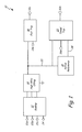
- FIG. 1 is a block diagram illustrating an overvoltage detection system according to an embodiment of the present invention.
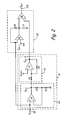
- FIG. 2 is a circuit diagram illustrating an active reference module and an overvoltage timed trip module according to an embodiment of the present invention.
- FIG. 3 is a chart illustrating an inverse time curve according to an embodiment of the present invention.
- FIG. 4 is a flowchart illustrating a method of detecting an overvoltage condition according to an embodiment of the present invention.
- the present invention describes a system and method for controlled overvoltage detection.
- the system includes an active reference circuit and an overvoltage timed trip circuit.
- the active reference circuit receives a sensed voltage and provides an output having a magnitude that varies inversely with a magnitude of the sensed voltage.
- the output of the active reference circuit is provided as input to the timed trip circuit. Because the active reference varies inversely with the sensed voltage, the overvoltage timed trip curve can be flattened below a traditional resistor-capacitor (RC) inverse time curve.
- RC resistor-capacitor
- FIG. 1 is a block diagram illustrating a system 10 for detecting an overvoltage condition.
- System 10 comprises a scaling module 12, a high-wins OR'ing module 14, an overvoltage fast trip module 16, an active reference module 18, and an overvoltage timed trip module 20, phase inputs 22a-22c, neutral input 24, overvoltage reference inputs 26a-26b, overvoltage reference line 28, sensed voltage line 30, and overvoltage outputs 32a-32b.
- AC alternating current
- DC direct current
- Scaling module 12 scales down phase inputs 22a-22c by any desired factor, such as 100.
- High-wins OR'ing module 14 converts the phase signals from AC to DC and selects the phase with the highest voltage using, for example, diode OR'ing.
- the output of high-wins OR'ing module 14 is a sensed DC voltage provided on sensed voltage line 30.
- Overvoltage fast trip module 16 indicates an overvoltage condition if the voltage on sensed voltage line 30 is larger than the voltage on overvoltage reference input 26a.
- the voltage on reference input 26a is defined by the system and can be any value for which an overvoltage condition should immediately be flagged.
- Overvoltage fast trip module 16 is implemented, for example, using a comparator.
- Active reference module 18 and timed trip module 20 act together to provide a time dependent overvoltage indication on overvoltage output 32b.
- Active reference module 18 receives input on sensed voltage line 30.
- Active reference module 18 provides output on overvoltage reference line 28 that is inversely proportional to the voltage on sensed voltage line 30. This output is provided to timed trip module 20 to be used as an active reference voltage.
- Timed trip module 20 is implemented using a resistor-capacitor (RC) circuit. The capacitor begins charging when the voltage on sensed voltage line 30 is larger than the voltage on overvoltage reference input 26b. The voltage across the capacitor is compared to the voltage on overvoltage reference line 28 in order to determine if an overvoltage condition is present.
- RC resistor-capacitor
- FIG. 2 is a circuit diagram illustrating an active reference module 18 and timed trip module 20 according to an embodiment of the present invention.
- Active reference module 18 is a circuit that includes non-inverting amplifier circuit 40, and inverting amplifier circuit 42.
- Non-inverting amplifier circuit 40 includes operational amplifier 44, resistors R1 and R2, and receives input on sensed voltage line 30 (V IN ).
- Inverting amplifier circuit 42 includes operational amplifier 46 and resistors R3 and R4.
- Timed trip module 20 is a circuit that includes capacitor C1, resistor R5, comparators 48 and 50, receives input on overvoltage reference input 26b (V REF2 ), and provides output on overvoltage output 32b (V OUT ).
- Non-inverting amplifier circuit 42 receives input voltage V IN .
- This input voltage is a sensed voltage and is provided to the non-inverting input of operational amplifier 44.
- This output is provided to inverting amplifier circuit 42.
- Resistor R3 is connected between V MID and the inverting input of operational amplifier 46.
- Resistor R4 is connected between the inverting input of operational amplifier 46 and the output of inverting amplifier 42, V REF1 .
- the non-inverting input of operational amplifier 46 is connected to a voltage V OFFSET which is defined by the system.
- V REF1 V OFFSET * (1 + R4/R3) - (R4/R3) * (V IN * (1 + R1/R2)). Therefore, as V IN increases, V REF1 decreases at a rate dependent upon selected values of V OFFSET , and R1-R4.
- Timed trip circuit 20 provides output V OUT that indicates an overvoltage fault.
- the sensed voltage, V IN is provided as input to comparator 48 along with an overvoltage reference V REF2 .
- Resistor R5 is connected between V IN and the output of comparator 48.
- Capacitor C1 is connected between the output of comparator 48 and ground. The voltage across the capacitor is input into comparator 50 along with V REF1.
- V IN is greater than V REF2
- capacitor C1 begins to charge.
- V IN is less than V REF2
- capacitor C1 discharges. If the voltage across capacitor C1 is ever larger than V REF1 , an overvoltage fault is indicated by the output of comparator 50.
- FIG. 3 is a chart illustrating an overvoltage trip curve 70 according to an embodiment of the present invention.
- Trip curve 70 represents a voltage V IN required to indicate an overvoltage condition over time for system 10.
- Dashed line 72 illustrates a value of voltage over time of V IN for which an overvoltage will be detected if active reference module 18 were removed and V REF1 simply equaled V REF2 .
- the primary advantage of adding active reference module 18 is shown in the difference between dashed line 72 and trip curve 70.
- the rate at which trip curve decreases over time can essentially be 'flattened,' lowering it below the standard RC rate of 1-[1/e ⁇ (t/ ⁇ )], allowing greater customizability of the system.
- V IN required at 1 ⁇ for a simple RC system is approximately V REF2 / 0.63. This value can be decreased, as illustrated, using active reference module 18 while keeping the same trip value, V REF2 , at 5 ⁇ .
- Dashed line 74 illustrates a further possible trip curve that could be obtained by adjusting the values of R1-R4 and V OFFSET .
- FIG. 4 is a flowchart illustrating a method 90 of detecting an overvoltage according to an embodiment of the present invention.
- a voltage is sensed by system 10. This voltage is provided to active reference module 18.
- active reference module 18 provides a reference voltage that is inversely proportional to the sensed voltage.
- it is determined if the voltage sensed by the system is greater than a fixed reference voltage. If it is, method 90 proceeds to step 96 and charges capacitor C1. If it is not, method 90 proceeds to step 98 and discharges the capacitor. Following step 98, method 90 returns to step 92.
- step 100 it is determined if the voltage across capacitor C1 is greater than the active reference voltage. If it is, method 90 proceeds to step 102 and indicates an overvoltage fault. If it is not, method 90 returns to step 92.
Landscapes
- Physics & Mathematics (AREA)
- General Physics & Mathematics (AREA)
- Protection Of Static Devices (AREA)
- Emergency Protection Circuit Devices (AREA)
Abstract
Description
- The present invention relates to overvoltage detection, and in particular to a system and method for controlled overvoltage detection.
- Electric power systems, such as those on an aircraft, are susceptible to overvoltage conditions. An overvoltage condition exists when the voltage applied to a load, for example, is larger than a voltage the load is rated to handle. These conditions may occur, for example, due to a lightning strike. If the voltage is large enough, or exists for long enough, permanent damage can be incurred by the system. Therefore, it is necessary to detect overvoltage conditions so that they may be handled prior to damaging the circuit.
- Aside from unpredictable occurrences such as lighting strikes, overvoltage conditions may occur due to predictable events such as removing or adding power to a load. These events can create transients within the power system that do not pose a threat to the system if their duration is short. These transients have a natural recovery time, and it is desirable to not indicate an overvoltage condition if the system recovers within this natural recovery time. Therefore, timed trip overvoltage detection has been implemented to accommodate these expected short transients.
- Timed trip overvoltage detection has been accomplished in the past using a simple resistor-capacitor (RC) circuit. A sensed voltage is input to the RC circuit, and the voltage across the capacitor is compared to a reference voltage. This reference voltage is generally set to a voltage that will cause an overvoltage indication at 5τ, where τ = R * C (i.e., when the capacitor is fully charged). Therefore, the higher the sensed voltage, the faster the capacitor will reach that trip threshold. This creates a "trip curve" where the necessary voltage to indicate an overvoltage fault decreases with time. The rate of change of the trip curve is equal to the rate of change of the voltage across the resistor of the RC circuit, which is approximately 1-[1/e^(t/τ)]. Because of this, using solely an RC circuit greatly limits control of the characteristics of the timed trip curve.
- An overvoltage detection system includes a sensed voltage, an active reference module, and a timed trip module. The active reference module generates an active reference signal that has a magnitude that varies inversely with a magnitude of the sensed voltage. The timed trip module includes a resistor and a capacitor, and detects an overvoltage condition as a function of the sensed voltage, the active reference signal, and time.
-
FIG. 1 is a block diagram illustrating an overvoltage detection system according to an embodiment of the present invention. -
FIG. 2 is a circuit diagram illustrating an active reference module and an overvoltage timed trip module according to an embodiment of the present invention. -
FIG. 3 is a chart illustrating an inverse time curve according to an embodiment of the present invention. -
FIG. 4 is a flowchart illustrating a method of detecting an overvoltage condition according to an embodiment of the present invention. - The present invention describes a system and method for controlled overvoltage detection. The system includes an active reference circuit and an overvoltage timed trip circuit. The active reference circuit receives a sensed voltage and provides an output having a magnitude that varies inversely with a magnitude of the sensed voltage. The output of the active reference circuit is provided as input to the timed trip circuit. Because the active reference varies inversely with the sensed voltage, the overvoltage timed trip curve can be flattened below a traditional resistor-capacitor (RC) inverse time curve.
-
FIG. 1 is a block diagram illustrating asystem 10 for detecting an overvoltage condition.System 10 comprises ascaling module 12, a high-wins OR'ingmodule 14, an overvoltagefast trip module 16, anactive reference module 18, and an overvoltagetimed trip module 20,phase inputs 22a-22c,neutral input 24,overvoltage reference inputs 26a-26b,overvoltage reference line 28, sensedvoltage line 30, andovervoltage outputs 32a-32b. Although illustrated as having three alternating current (AC)phase inputs 22a-22c,system 10 can be implemented with any number of phase inputs, both AC and direct current (DC).Scaling module 12 scales downphase inputs 22a-22c by any desired factor, such as 100. High-wins OR'ingmodule 14 converts the phase signals from AC to DC and selects the phase with the highest voltage using, for example, diode OR'ing. The output of high-wins OR'ingmodule 14 is a sensed DC voltage provided on sensedvoltage line 30. - If the DC voltage on sensed
voltage line 30 is large enough,system 10 will immediately indicate an overvoltage condition onovervoltage output 32a. Overvoltagefast trip module 16 indicates an overvoltage condition if the voltage on sensedvoltage line 30 is larger than the voltage onovervoltage reference input 26a. The voltage onreference input 26a is defined by the system and can be any value for which an overvoltage condition should immediately be flagged. Overvoltagefast trip module 16 is implemented, for example, using a comparator. -
Active reference module 18 and timedtrip module 20 act together to provide a time dependent overvoltage indication onovervoltage output 32b.Active reference module 18 receives input on sensedvoltage line 30.Active reference module 18 provides output onovervoltage reference line 28 that is inversely proportional to the voltage on sensedvoltage line 30. This output is provided to timedtrip module 20 to be used as an active reference voltage.Timed trip module 20 is implemented using a resistor-capacitor (RC) circuit. The capacitor begins charging when the voltage on sensedvoltage line 30 is larger than the voltage onovervoltage reference input 26b. The voltage across the capacitor is compared to the voltage onovervoltage reference line 28 in order to determine if an overvoltage condition is present. -
FIG. 2 is a circuit diagram illustrating anactive reference module 18 and timedtrip module 20 according to an embodiment of the present invention.Active reference module 18 is a circuit that includesnon-inverting amplifier circuit 40, and invertingamplifier circuit 42.Non-inverting amplifier circuit 40 includesoperational amplifier 44, resistors R1 and R2, and receives input on sensed voltage line 30 (VIN). Invertingamplifier circuit 42 includesoperational amplifier 46 and resistors R3 and R4.Timed trip module 20 is a circuit that includes capacitor C1, resistor R5,comparators overvoltage reference input 26b (VREF2), and provides output onovervoltage output 32b (VOUT). - Non-inverting
amplifier circuit 42 receives input voltage VIN. This input voltage is a sensed voltage and is provided to the non-inverting input ofoperational amplifier 44. The inverting input ofoperational amplifier 44 is connected to ground. Therefore, the output voltage ofnon-inverting amplifier circuit 42 is VMID = VIN * (1 + R1/R2). This output is provided to invertingamplifier circuit 42. Resistor R3 is connected between VMID and the inverting input ofoperational amplifier 46. Resistor R4 is connected between the inverting input ofoperational amplifier 46 and the output of invertingamplifier 42, VREF1. The non-inverting input ofoperational amplifier 46 is connected to a voltage VOFFSET which is defined by the system. Thus, the transfer function foractive reference circuit 18 is: VREF1 = VOFFSET * (1 + R4/R3) - (R4/R3) * (VIN * (1 + R1/R2)). Therefore, as VIN increases, VREF1 decreases at a rate dependent upon selected values of VOFFSET, and R1-R4. -
Timed trip circuit 20 provides output VOUT that indicates an overvoltage fault. The sensed voltage, VIN, is provided as input tocomparator 48 along with an overvoltage reference VREF2. Resistor R5 is connected between VIN and the output ofcomparator 48. Capacitor C1 is connected between the output ofcomparator 48 and ground. The voltage across the capacitor is input intocomparator 50 along with VREF1. When VIN is greater than VREF2, capacitor C1 begins to charge. When VIN is less than VREF2, capacitor C1 discharges. If the voltage across capacitor C1 is ever larger than VREF1, an overvoltage fault is indicated by the output ofcomparator 50. Therefore, if the voltage at VIN is greater than VREF2 for a long enough time period, an overvoltage fault will be indicated. Because ofactive reference module 18, the larger VIN is, the lower the voltage across capacitor C1 needs to be in order to detect an overvoltage fault. -
FIG. 3 is a chart illustrating anovervoltage trip curve 70 according to an embodiment of the present invention.Trip curve 70 represents a voltage VIN required to indicate an overvoltage condition over time forsystem 10. Dashedline 72 illustrates a value of voltage over time of VIN for which an overvoltage will be detected ifactive reference module 18 were removed and VREF1 simply equaled VREF2. This time curve is an RC time curve that decreases at a rate of approximately 1-[1/e^(t/τ)], where τ = R5 * C1. At t=5τ , the capacitor is essentially fully charged. The primary advantage of addingactive reference module 18 is shown in the difference between dashedline 72 andtrip curve 70. By providing an active reference that varies inversely with the sensed voltage, the rate at which trip curve decreases over time can essentially be 'flattened,' lowering it below the standard RC rate of 1-[1/e^(t/τ)], allowing greater customizability of the system. For example, the voltage VIN required at 1τ for a simple RC system is approximately VREF2 / 0.63. This value can be decreased, as illustrated, usingactive reference module 18 while keeping the same trip value, VREF2, at 5τ. Dashedline 74 illustrates a further possible trip curve that could be obtained by adjusting the values of R1-R4 and VOFFSET. -
FIG. 4 is a flowchart illustrating amethod 90 of detecting an overvoltage according to an embodiment of the present invention. Atstep 92, a voltage is sensed bysystem 10. This voltage is provided toactive reference module 18. Atstep 92,active reference module 18 provides a reference voltage that is inversely proportional to the sensed voltage. Atstep 94, it is determined if the voltage sensed by the system is greater than a fixed reference voltage. If it is,method 90 proceeds to step 96 and charges capacitor C1. If it is not,method 90 proceeds to step 98 and discharges the capacitor. Followingstep 98,method 90 returns to step 92. Atstep 100, it is determined if the voltage across capacitor C1 is greater than the active reference voltage. If it is,method 90 proceeds to step 102 and indicates an overvoltage fault. If it is not,method 90 returns to step 92. - In this way, the present invention describes a controlled overvoltage detection system. Although the present invention has been described with reference to preferred embodiments, workers skilled in the art will recognize that changes may be made in form and detail without departing from the scope of the invention, which is defined by the claims.
Claims (11)
- An overvoltage detection system comprising:a sensed voltage line for providing a sensed voltage;an active reference module that generates an active reference signal having a magnitude that varies inversely with a magnitude of the sensed voltage; anda timed trip module that includes a reference resistor and a capacitor, wherein the timed trip module detects an overvoltage condition as a function of the sensed voltage, the active reference signal, and time.
- The system of claim 1, wherein a voltage required for the timed trip module to detect an overvoltage condition decreases at a rate less than 1-[1/e^(t/τ)] between t=1τ and t=5τ seconds from when the capacitor begins to charge, wherein t is time and τ is equal to a resistance of the reference resistor multiplied by a capacitance of the capacitor.
- The system of claim 1 or 2, wherein the active reference module comprises:a non-inverting amplifier that receives the sensed voltage as input; andan inverting amplifier that receives an output of the non-inverting amplifier as its inverting input and an offset voltage as its non-inverting input, wherein the active reference signal is output from the inverting amplifier.
- The system of claim 3, wherein the transfer function of the active reference module is:VREF = VOFFSET * (1 + R4/R3) - (R4/R3) * (VIN * (1 + R1/R2)) wherein:VREF = the active reference signal;VOFFSET = the offset voltage;R1 = a first reference resistor of the non-inverting amplifier;R2 = a second reference resistor of the non-inverting amplifier;R3 = a first reference resistor of the inverting amplifier;R4 = a second reference resistor of the inverting amplifier; andVIN = the sensed voltage.
- The system of claim 1, 2, 3 or 4, wherein the timed trip module comprises:a first comparator, wherein when the sensed voltage is larger than a fixed reference voltage, the capacitor begins to charge; anda second comparator, wherein when a voltage across the capacitor is larger than the active reference signal, the output of the comparator indicates an overvoltage fault.
- The system of any preceding claim, further comprising:a scaling module for scaling down a three-phase AC input voltage; anda high-wins OR'ing module for converting the scaled three-phase AC input voltage into a single DC voltage, wherein the sensed voltage is equal to the single DC voltage.
- The system of claim 6, further comprising a fast trip module for immediately detecting an overvoltage fault if the sensed voltage is greater than a fast trip reference voltage.
- A method of detecting an overvoltage, the method comprising:monitoring a voltage;actively controlling an active reference voltage, wherein a magnitude of the active reference voltage varies inversely with a magnitude of the monitored voltage;charging a capacitor if the monitored voltage is larger than a fixed reference voltage; andindicating an overvoltage fault if a voltage across the capacitor is larger than the active reference voltage.
- The method of claim 8, wherein actively controlling an active reference voltage comprises:inputting the monitored voltage into a non-inverting input of a non-inverting amplifier; andinputting an output of the non-inverting amplifier into an inverting input of an inverting amplifier, wherein an offset voltage is input into a non-inverting input of the inverting amplifier.
- The method of claim 8 or 9, wherein charging a capacitor if the monitored voltage is larger than a fixed reference voltage comprises:comparing the monitored voltage with the fixed reference voltage;charging the capacitor using the monitored voltage if the monitored voltage is greater than the fixed reference voltage; anddischarging the capacitor if the monitored voltage is less than the fixed reference voltage.
- The method of claim 8, 9 or 10, wherein monitoring a voltage comprises:scaling down a three-phase voltage by a predetermined factor; andselecting the phase with the greatest amplitude and converting the selected phase to a DC voltage, wherein the DC voltage is provided as the monitored voltage.
Applications Claiming Priority (1)
| Application Number | Priority Date | Filing Date | Title |
|---|---|---|---|
| US13/495,457 US8929044B2 (en) | 2012-06-13 | 2012-06-13 | System and method for controlled overvoltage detection |
Publications (3)
| Publication Number | Publication Date |
|---|---|
| EP2674767A2 true EP2674767A2 (en) | 2013-12-18 |
| EP2674767A3 EP2674767A3 (en) | 2015-08-12 |
| EP2674767B1 EP2674767B1 (en) | 2019-09-11 |
Family
ID=47912951
Family Applications (1)
| Application Number | Title | Priority Date | Filing Date |
|---|---|---|---|
| EP13157943.5A Active EP2674767B1 (en) | 2012-06-13 | 2013-03-06 | System and method for controlled overvoltage detection |
Country Status (2)
| Country | Link |
|---|---|
| US (1) | US8929044B2 (en) |
| EP (1) | EP2674767B1 (en) |
Families Citing this family (2)
| Publication number | Priority date | Publication date | Assignee | Title |
|---|---|---|---|---|
| CN104749454A (en) * | 2013-12-30 | 2015-07-01 | 上海普锐马电子有限公司 | Program-controlled monitoring circuit for high voltage capacitor |
| US10139454B2 (en) | 2016-01-20 | 2018-11-27 | Test Research, Inc. | Test device and alternating current power detection method of the same |
Family Cites Families (8)
| Publication number | Priority date | Publication date | Assignee | Title |
|---|---|---|---|---|
| US3480834A (en) * | 1966-09-19 | 1969-11-25 | Westinghouse Electric Corp | Miniature overvoltage protection circuit having separate voltage sensing and time delay circuits |
| US3944890A (en) * | 1974-09-10 | 1976-03-16 | General Electric Co. | Static overcurrent relay |
| FR2530089A1 (en) * | 1982-07-12 | 1984-01-13 | Merlin Gerin | ANALOGUE ELECTRONIC SENSOR FOR CIRCUIT BREAKER AGAINST OVERCURRENT OF AN ALTERNATING CURRENT NETWORK |
| US5073724A (en) * | 1990-07-18 | 1991-12-17 | Westinghouse Electric Corp. | Programmable inverse time delay circuit |
| US5276434A (en) * | 1992-04-03 | 1994-01-04 | Brooks Elgin C | Carbon monoxide concentration indicator and alarm |
| JP2003317982A (en) * | 2002-04-19 | 2003-11-07 | Hitachi Media Electoronics Co Ltd | Discharge lamp lighting device |
| KR100714633B1 (en) * | 2006-06-20 | 2007-05-07 | 삼성전기주식회사 | LC backlight inverter |
| US8232778B1 (en) * | 2011-01-28 | 2012-07-31 | Hamilton Sundstrand Corporation | Independent, redundant overvoltage protection for a generator |
-
2012
- 2012-06-13 US US13/495,457 patent/US8929044B2/en active Active
-
2013
- 2013-03-06 EP EP13157943.5A patent/EP2674767B1/en active Active
Non-Patent Citations (1)
| Title |
|---|
| None |
Also Published As
| Publication number | Publication date |
|---|---|
| US8929044B2 (en) | 2015-01-06 |
| EP2674767A3 (en) | 2015-08-12 |
| EP2674767B1 (en) | 2019-09-11 |
| US20130335872A1 (en) | 2013-12-19 |
Similar Documents
| Publication | Publication Date | Title |
|---|---|---|
| US7408750B2 (en) | Methods of detecting arc faults characterized by consecutive periods of arcing | |
| US7898781B2 (en) | Arc fault detection apparatus employing a comparator with a continuously variable threshold | |
| EP2309280B1 (en) | Ground fault sensing device | |
| EP2999075B1 (en) | Power supply with surge voltage protection | |
| US10890606B2 (en) | Detection circuit for an active discharge circuit of an X-capacitor, related active discharge circuit, integrated circuit and method | |
| CN102749498B (en) | Alternating voltage detection circuit and method thereof and safety capacitor discharge circuit | |
| EP2762903B1 (en) | Ac input voltage interruption detection method and circuit | |
| CN107211499B (en) | Driver circuits capable of monitoring the use of surge protection arrangements | |
| TW201021379A (en) | Protection apparatus and method for boost converter | |
| EP2808194B1 (en) | Loose plug detection | |
| US10916939B2 (en) | Low leakage transient overvoltage protection circuit using a series connected metal oxide varistor (MOV) and silicon controlled rectifier (SCR) | |
| US8929044B2 (en) | System and method for controlled overvoltage detection | |
| CN101673937A (en) | Surge interference identification method during differential protection and differential protection method | |
| CN203813421U (en) | Photovoltaic energy-storage inversion control integrated machine short-circuit and overload protecting circuit | |
| US10114048B2 (en) | Detection circuit | |
| JP6569489B2 (en) | Semiconductor integrated circuit for earth leakage breaker | |
| CN103715662A (en) | Short circuit and overload protection circuit of photovoltaic energy storage inverse control all-in-one machine | |
| CN111208360A (en) | Detection circuit, system and consumer | |
| CN108141146B (en) | Power converter | |
| CN211402683U (en) | Overcurrent protection detection circuit | |
| KR101434435B1 (en) | Inverter DC Link Voltage Control System And Method Thereof | |
| EP3499705B1 (en) | Creeping discharge element drive device and creeping discharge element drive method | |
| US12592557B2 (en) | Pre-charge short circuit detection | |
| CN103762545B (en) | A kind of multi-stage controllable current protection circuit | |
| JPS6229962B2 (en) |
Legal Events
| Date | Code | Title | Description |
|---|---|---|---|
| PUAI | Public reference made under article 153(3) epc to a published international application that has entered the european phase |
Free format text: ORIGINAL CODE: 0009012 |
|
| AK | Designated contracting states |
Kind code of ref document: A2 Designated state(s): AL AT BE BG CH CY CZ DE DK EE ES FI FR GB GR HR HU IE IS IT LI LT LU LV MC MK MT NL NO PL PT RO RS SE SI SK SM TR |
|
| AX | Request for extension of the european patent |
Extension state: BA ME |
|
| PUAL | Search report despatched |
Free format text: ORIGINAL CODE: 0009013 |
|
| AK | Designated contracting states |
Kind code of ref document: A3 Designated state(s): AL AT BE BG CH CY CZ DE DK EE ES FI FR GB GR HR HU IE IS IT LI LT LU LV MC MK MT NL NO PL PT RO RS SE SI SK SM TR |
|
| AX | Request for extension of the european patent |
Extension state: BA ME |
|
| RIC1 | Information provided on ipc code assigned before grant |
Ipc: G01R 19/25 20060101ALI20150703BHEP Ipc: H02H 3/22 20060101ALN20150703BHEP Ipc: G01R 19/165 20060101AFI20150703BHEP |
|
| 17P | Request for examination filed |
Effective date: 20160209 |
|
| RBV | Designated contracting states (corrected) |
Designated state(s): AL AT BE BG CH CY CZ DE DK EE ES FI FR GB GR HR HU IE IS IT LI LT LU LV MC MK MT NL NO PL PT RO RS SE SI SK SM TR |
|
| GRAP | Despatch of communication of intention to grant a patent |
Free format text: ORIGINAL CODE: EPIDOSNIGR1 |
|
| STAA | Information on the status of an ep patent application or granted ep patent |
Free format text: STATUS: GRANT OF PATENT IS INTENDED |
|
| RIC1 | Information provided on ipc code assigned before grant |
Ipc: H02H 3/027 20060101ALN20190218BHEP Ipc: H02H 1/00 20060101ALI20190218BHEP Ipc: H02H 3/20 20060101ALN20190218BHEP Ipc: G01R 19/165 20060101AFI20190218BHEP Ipc: G01R 19/25 20060101ALI20190218BHEP |
|
| INTG | Intention to grant announced |
Effective date: 20190320 |
|
| GRAS | Grant fee paid |
Free format text: ORIGINAL CODE: EPIDOSNIGR3 |
|
| GRAA | (expected) grant |
Free format text: ORIGINAL CODE: 0009210 |
|
| STAA | Information on the status of an ep patent application or granted ep patent |
Free format text: STATUS: THE PATENT HAS BEEN GRANTED |
|
| AK | Designated contracting states |
Kind code of ref document: B1 Designated state(s): AL AT BE BG CH CY CZ DE DK EE ES FI FR GB GR HR HU IE IS IT LI LT LU LV MC MK MT NL NO PL PT RO RS SE SI SK SM TR |
|
| REG | Reference to a national code |
Ref country code: GB Ref legal event code: FG4D |
|
| REG | Reference to a national code |
Ref country code: CH Ref legal event code: EP |
|
| REG | Reference to a national code |
Ref country code: AT Ref legal event code: REF Ref document number: 1179135 Country of ref document: AT Kind code of ref document: T Effective date: 20190915 |
|
| REG | Reference to a national code |
Ref country code: DE Ref legal event code: R096 Ref document number: 602013060263 Country of ref document: DE Ref country code: IE Ref legal event code: FG4D |
|
| REG | Reference to a national code |
Ref country code: NL Ref legal event code: MP Effective date: 20190911 |
|
| REG | Reference to a national code |
Ref country code: LT Ref legal event code: MG4D |
|
| PG25 | Lapsed in a contracting state [announced via postgrant information from national office to epo] |
Ref country code: FI Free format text: LAPSE BECAUSE OF FAILURE TO SUBMIT A TRANSLATION OF THE DESCRIPTION OR TO PAY THE FEE WITHIN THE PRESCRIBED TIME-LIMIT Effective date: 20190911 Ref country code: NO Free format text: LAPSE BECAUSE OF FAILURE TO SUBMIT A TRANSLATION OF THE DESCRIPTION OR TO PAY THE FEE WITHIN THE PRESCRIBED TIME-LIMIT Effective date: 20191211 Ref country code: SE Free format text: LAPSE BECAUSE OF FAILURE TO SUBMIT A TRANSLATION OF THE DESCRIPTION OR TO PAY THE FEE WITHIN THE PRESCRIBED TIME-LIMIT Effective date: 20190911 Ref country code: BG Free format text: LAPSE BECAUSE OF FAILURE TO SUBMIT A TRANSLATION OF THE DESCRIPTION OR TO PAY THE FEE WITHIN THE PRESCRIBED TIME-LIMIT Effective date: 20191211 Ref country code: HR Free format text: LAPSE BECAUSE OF FAILURE TO SUBMIT A TRANSLATION OF THE DESCRIPTION OR TO PAY THE FEE WITHIN THE PRESCRIBED TIME-LIMIT Effective date: 20190911 Ref country code: LT Free format text: LAPSE BECAUSE OF FAILURE TO SUBMIT A TRANSLATION OF THE DESCRIPTION OR TO PAY THE FEE WITHIN THE PRESCRIBED TIME-LIMIT Effective date: 20190911 |
|
| PG25 | Lapsed in a contracting state [announced via postgrant information from national office to epo] |
Ref country code: RS Free format text: LAPSE BECAUSE OF FAILURE TO SUBMIT A TRANSLATION OF THE DESCRIPTION OR TO PAY THE FEE WITHIN THE PRESCRIBED TIME-LIMIT Effective date: 20190911 Ref country code: ES Free format text: LAPSE BECAUSE OF FAILURE TO SUBMIT A TRANSLATION OF THE DESCRIPTION OR TO PAY THE FEE WITHIN THE PRESCRIBED TIME-LIMIT Effective date: 20190911 Ref country code: AL Free format text: LAPSE BECAUSE OF FAILURE TO SUBMIT A TRANSLATION OF THE DESCRIPTION OR TO PAY THE FEE WITHIN THE PRESCRIBED TIME-LIMIT Effective date: 20190911 Ref country code: GR Free format text: LAPSE BECAUSE OF FAILURE TO SUBMIT A TRANSLATION OF THE DESCRIPTION OR TO PAY THE FEE WITHIN THE PRESCRIBED TIME-LIMIT Effective date: 20191212 Ref country code: LV Free format text: LAPSE BECAUSE OF FAILURE TO SUBMIT A TRANSLATION OF THE DESCRIPTION OR TO PAY THE FEE WITHIN THE PRESCRIBED TIME-LIMIT Effective date: 20190911 |
|
| REG | Reference to a national code |
Ref country code: AT Ref legal event code: MK05 Ref document number: 1179135 Country of ref document: AT Kind code of ref document: T Effective date: 20190911 |
|
| PG25 | Lapsed in a contracting state [announced via postgrant information from national office to epo] |
Ref country code: PL Free format text: LAPSE BECAUSE OF FAILURE TO SUBMIT A TRANSLATION OF THE DESCRIPTION OR TO PAY THE FEE WITHIN THE PRESCRIBED TIME-LIMIT Effective date: 20190911 Ref country code: EE Free format text: LAPSE BECAUSE OF FAILURE TO SUBMIT A TRANSLATION OF THE DESCRIPTION OR TO PAY THE FEE WITHIN THE PRESCRIBED TIME-LIMIT Effective date: 20190911 Ref country code: PT Free format text: LAPSE BECAUSE OF FAILURE TO SUBMIT A TRANSLATION OF THE DESCRIPTION OR TO PAY THE FEE WITHIN THE PRESCRIBED TIME-LIMIT Effective date: 20200113 Ref country code: RO Free format text: LAPSE BECAUSE OF FAILURE TO SUBMIT A TRANSLATION OF THE DESCRIPTION OR TO PAY THE FEE WITHIN THE PRESCRIBED TIME-LIMIT Effective date: 20190911 Ref country code: IT Free format text: LAPSE BECAUSE OF FAILURE TO SUBMIT A TRANSLATION OF THE DESCRIPTION OR TO PAY THE FEE WITHIN THE PRESCRIBED TIME-LIMIT Effective date: 20190911 Ref country code: NL Free format text: LAPSE BECAUSE OF FAILURE TO SUBMIT A TRANSLATION OF THE DESCRIPTION OR TO PAY THE FEE WITHIN THE PRESCRIBED TIME-LIMIT Effective date: 20190911 Ref country code: AT Free format text: LAPSE BECAUSE OF FAILURE TO SUBMIT A TRANSLATION OF THE DESCRIPTION OR TO PAY THE FEE WITHIN THE PRESCRIBED TIME-LIMIT Effective date: 20190911 |
|
| PG25 | Lapsed in a contracting state [announced via postgrant information from national office to epo] |
Ref country code: SK Free format text: LAPSE BECAUSE OF FAILURE TO SUBMIT A TRANSLATION OF THE DESCRIPTION OR TO PAY THE FEE WITHIN THE PRESCRIBED TIME-LIMIT Effective date: 20190911 Ref country code: SM Free format text: LAPSE BECAUSE OF FAILURE TO SUBMIT A TRANSLATION OF THE DESCRIPTION OR TO PAY THE FEE WITHIN THE PRESCRIBED TIME-LIMIT Effective date: 20190911 Ref country code: CZ Free format text: LAPSE BECAUSE OF FAILURE TO SUBMIT A TRANSLATION OF THE DESCRIPTION OR TO PAY THE FEE WITHIN THE PRESCRIBED TIME-LIMIT Effective date: 20190911 Ref country code: IS Free format text: LAPSE BECAUSE OF FAILURE TO SUBMIT A TRANSLATION OF THE DESCRIPTION OR TO PAY THE FEE WITHIN THE PRESCRIBED TIME-LIMIT Effective date: 20200224 |
|
| REG | Reference to a national code |
Ref country code: DE Ref legal event code: R097 Ref document number: 602013060263 Country of ref document: DE |
|
| PLBE | No opposition filed within time limit |
Free format text: ORIGINAL CODE: 0009261 |
|
| STAA | Information on the status of an ep patent application or granted ep patent |
Free format text: STATUS: NO OPPOSITION FILED WITHIN TIME LIMIT |
|
| PG2D | Information on lapse in contracting state deleted |
Ref country code: IS |
|
| PG25 | Lapsed in a contracting state [announced via postgrant information from national office to epo] |
Ref country code: DK Free format text: LAPSE BECAUSE OF FAILURE TO SUBMIT A TRANSLATION OF THE DESCRIPTION OR TO PAY THE FEE WITHIN THE PRESCRIBED TIME-LIMIT Effective date: 20190911 Ref country code: IS Free format text: LAPSE BECAUSE OF FAILURE TO SUBMIT A TRANSLATION OF THE DESCRIPTION OR TO PAY THE FEE WITHIN THE PRESCRIBED TIME-LIMIT Effective date: 20200112 |
|
| 26N | No opposition filed |
Effective date: 20200615 |
|
| PG25 | Lapsed in a contracting state [announced via postgrant information from national office to epo] |
Ref country code: SI Free format text: LAPSE BECAUSE OF FAILURE TO SUBMIT A TRANSLATION OF THE DESCRIPTION OR TO PAY THE FEE WITHIN THE PRESCRIBED TIME-LIMIT Effective date: 20190911 |
|
| REG | Reference to a national code |
Ref country code: DE Ref legal event code: R119 Ref document number: 602013060263 Country of ref document: DE |
|
| PG25 | Lapsed in a contracting state [announced via postgrant information from national office to epo] |
Ref country code: MC Free format text: LAPSE BECAUSE OF FAILURE TO SUBMIT A TRANSLATION OF THE DESCRIPTION OR TO PAY THE FEE WITHIN THE PRESCRIBED TIME-LIMIT Effective date: 20190911 |
|
| REG | Reference to a national code |
Ref country code: CH Ref legal event code: PL |
|
| REG | Reference to a national code |
Ref country code: BE Ref legal event code: MM Effective date: 20200331 |
|
| PG25 | Lapsed in a contracting state [announced via postgrant information from national office to epo] |
Ref country code: LU Free format text: LAPSE BECAUSE OF NON-PAYMENT OF DUE FEES Effective date: 20200306 |
|
| PG25 | Lapsed in a contracting state [announced via postgrant information from national office to epo] |
Ref country code: CH Free format text: LAPSE BECAUSE OF NON-PAYMENT OF DUE FEES Effective date: 20200331 Ref country code: IE Free format text: LAPSE BECAUSE OF NON-PAYMENT OF DUE FEES Effective date: 20200306 Ref country code: DE Free format text: LAPSE BECAUSE OF NON-PAYMENT OF DUE FEES Effective date: 20201001 Ref country code: LI Free format text: LAPSE BECAUSE OF NON-PAYMENT OF DUE FEES Effective date: 20200331 |
|
| PG25 | Lapsed in a contracting state [announced via postgrant information from national office to epo] |
Ref country code: BE Free format text: LAPSE BECAUSE OF NON-PAYMENT OF DUE FEES Effective date: 20200331 |
|
| PG25 | Lapsed in a contracting state [announced via postgrant information from national office to epo] |
Ref country code: TR Free format text: LAPSE BECAUSE OF FAILURE TO SUBMIT A TRANSLATION OF THE DESCRIPTION OR TO PAY THE FEE WITHIN THE PRESCRIBED TIME-LIMIT Effective date: 20190911 Ref country code: MT Free format text: LAPSE BECAUSE OF FAILURE TO SUBMIT A TRANSLATION OF THE DESCRIPTION OR TO PAY THE FEE WITHIN THE PRESCRIBED TIME-LIMIT Effective date: 20190911 Ref country code: CY Free format text: LAPSE BECAUSE OF FAILURE TO SUBMIT A TRANSLATION OF THE DESCRIPTION OR TO PAY THE FEE WITHIN THE PRESCRIBED TIME-LIMIT Effective date: 20190911 |
|
| PG25 | Lapsed in a contracting state [announced via postgrant information from national office to epo] |
Ref country code: MK Free format text: LAPSE BECAUSE OF FAILURE TO SUBMIT A TRANSLATION OF THE DESCRIPTION OR TO PAY THE FEE WITHIN THE PRESCRIBED TIME-LIMIT Effective date: 20190911 |
|
| P01 | Opt-out of the competence of the unified patent court (upc) registered |
Effective date: 20230522 |
|
| PGFP | Annual fee paid to national office [announced via postgrant information from national office to epo] |
Ref country code: GB Payment date: 20260219 Year of fee payment: 14 |
|
| PGFP | Annual fee paid to national office [announced via postgrant information from national office to epo] |
Ref country code: FR Payment date: 20260220 Year of fee payment: 14 |