EP2672244A1 - Phase-locked delay device including an optical wedge pair - Google Patents
Phase-locked delay device including an optical wedge pair Download PDFInfo
- Publication number
- EP2672244A1 EP2672244A1 EP13168800.4A EP13168800A EP2672244A1 EP 2672244 A1 EP2672244 A1 EP 2672244A1 EP 13168800 A EP13168800 A EP 13168800A EP 2672244 A1 EP2672244 A1 EP 2672244A1
- Authority
- EP
- European Patent Office
- Prior art keywords
- pulse
- delay
- optical
- wedge
- input
- Prior art date
- Legal status (The legal status is an assumption and is not a legal conclusion. Google has not performed a legal analysis and makes no representation as to the accuracy of the status listed.)
- Granted
Links
Images





Classifications
-
- G—PHYSICS
- G01—MEASURING; TESTING
- G01J—MEASUREMENT OF INTENSITY, VELOCITY, SPECTRAL CONTENT, POLARISATION, PHASE OR PULSE CHARACTERISTICS OF INFRARED, VISIBLE OR ULTRAVIOLET LIGHT; COLORIMETRY; RADIATION PYROMETRY
- G01J3/00—Spectrometry; Spectrophotometry; Monochromators; Measuring colours
- G01J3/28—Investigating the spectrum
- G01J3/2889—Rapid scan spectrometers; Time resolved spectrometry
-
- G—PHYSICS
- G01—MEASURING; TESTING
- G01J—MEASUREMENT OF INTENSITY, VELOCITY, SPECTRAL CONTENT, POLARISATION, PHASE OR PULSE CHARACTERISTICS OF INFRARED, VISIBLE OR ULTRAVIOLET LIGHT; COLORIMETRY; RADIATION PYROMETRY
- G01J11/00—Measuring the characteristics of individual optical pulses or of optical pulse trains
-
- G—PHYSICS
- G01—MEASURING; TESTING
- G01J—MEASUREMENT OF INTENSITY, VELOCITY, SPECTRAL CONTENT, POLARISATION, PHASE OR PULSE CHARACTERISTICS OF INFRARED, VISIBLE OR ULTRAVIOLET LIGHT; COLORIMETRY; RADIATION PYROMETRY
- G01J3/00—Spectrometry; Spectrophotometry; Monochromators; Measuring colours
- G01J3/28—Investigating the spectrum
- G01J3/42—Absorption spectrometry; Double beam spectrometry; Flicker spectrometry; Reflection spectrometry
- G01J3/433—Modulation spectrometry; Derivative spectrometry
-
- G—PHYSICS
- G01—MEASURING; TESTING
- G01J—MEASUREMENT OF INTENSITY, VELOCITY, SPECTRAL CONTENT, POLARISATION, PHASE OR PULSE CHARACTERISTICS OF INFRARED, VISIBLE OR ULTRAVIOLET LIGHT; COLORIMETRY; RADIATION PYROMETRY
- G01J3/00—Spectrometry; Spectrophotometry; Monochromators; Measuring colours
- G01J3/28—Investigating the spectrum
- G01J3/45—Interferometric spectrometry
- G01J3/453—Interferometric spectrometry by correlation of the amplitudes
-
- H—ELECTRICITY
- H01—ELECTRIC ELEMENTS
- H01S—DEVICES USING THE PROCESS OF LIGHT AMPLIFICATION BY STIMULATED EMISSION OF RADIATION [LASER] TO AMPLIFY OR GENERATE LIGHT; DEVICES USING STIMULATED EMISSION OF ELECTROMAGNETIC RADIATION IN WAVE RANGES OTHER THAN OPTICAL
- H01S3/00—Lasers, i.e. devices using stimulated emission of electromagnetic radiation in the infrared, visible or ultraviolet wave range
- H01S3/005—Optical devices external to the laser cavity, specially adapted for lasers, e.g. for homogenisation of the beam or for manipulating laser pulses, e.g. pulse shaping
Definitions
- This disclosure relates to techniques for generating collinear and phase-locked replicas of an electromagnetic radiation pulse.
- 2D optical spectroscopy An important application that calls for a pair of phase-locked pulses is the so called Two-dimensional (2D) optical spectroscopy.
- This technique is used by a growing community of physicists, chemists and biologists both in the infrared (IR) range, targeting vibrational transitions (2DIR spectroscopy), and in the visible range, targeting electronic transitions (2D electronic spectroscopy).
- 2D spectroscopy uses a pump-probe geometry with two phase-locked collinear pulses exciting the sample, which is then probed by a third non-collinear pulse.
- a second application concerns the FTIR (Fourier Transform infrared) spectrometry.
- FTIR Fast Fourier Transform infrared
- phase-locked delayed pulse replicas is currently performed by means of two main techniques.
- the first technique is based on the Michelson interferometer according to which an interference pattern is produced by splitting a beam of light into two paths, bouncing the beams back and recombining them.
- This technique requires complex feedback circuits to keep the interferometer in stability conditions. Moreover, higher feedback accuracy is required for shorter wavelengths; therefore, it is observed that the Michelson interferometer method does not appear satisfying for generating pulse replicas of radiation with sub-wavelength accuracy.
- the second known technique is based on a "pulse shaper" which generates the pulse replicas by suitably applying spectral amplitude modulation and spectral phase modulation to a pulse.
- This technique appears particularly complex and expensive.
- Document US-2009-0161092 describes an optical device employed to generate delayed pulse replicas to be employed in a multidimensional spectrometer.
- the Babinet-Soleil compensator is a continuously variable, zero-order retarder employing a birefringent wedge which is movable and another birefringent wedge which is fixed to a compensator plate.
- the orientation of the long axis of the wedges is perpendicular to the long axis of the compensator plate.
- the known Babinet-Soleil compensators are employed in optics to introduce phase delays between two orthogonal polarizations of an electromagnetic field; such phase delays are limited to one optical cycle (e.g. a maximum phase delay of 5.5 fs at 1650 nm) and their effect is to rotate the polarization or act as phase equalizers. Movement of the birefringent wedge is required in order to tune the device to the given electromagnetic field frequency.
- a phase-locked delay device comprises:
- FIG. 1 shows a first embodiment of a phase-locked delay device 100.
- the phase-locked delay device 100 (hereinafter also “delay device”) is configured to generate two delayed, collinear replicas of an input electromagnetic radiation pulse.
- delay device With reference to the optical structure of the delay device 100, the following axes/directions can be defined:
- the first direction x and the second direction y define a plane which is orthogonal to the propagation direction z.
- the delay device 100 includes an adjustable Babinet-Soleil module 1 which is an optical device comprising optical components in birefringent material/s.
- an electromagnetic field can be always decomposed in the sum of two independent fields with orthogonal polarizations.
- the directions of such polarizations are determined by the structure of the material; the two orthogonal directions are named the "fast” and the “slow” polarization directions.
- the radiation having linear polarization along the fast direction sees the fast refractive index n f and travels with the fast group velocity v gf and the fast phase velocity v pf .
- the radiation having linear polarization along the slow direction sees the slow refractive index n s and travels with the slow group velocity v gs and the slow phase velocity v ps .
- Birefringent materials are classified "biaxial birefringent materials" when the two optical axes have different orientations in space, and “uniaxial birefringent materials” when the two optical axes degenerate in one axis only.
- the Babinet-Soleil module 1 defines, in accordance with the embodiment described, a first slow polarization direction OX1 parallel to the first direction x and a second slow polarization direction OX2 parallel to second direction y.
- the Babinet-Soleil module 1 is provided with an input port 2 and an output port 3.
- the delay device 100 can be configured to operate on pulses having carrier radiation at wavelength ⁇ comprised at least in the following range: 200 nm - 15000 nm (from the ultraviolet to the mid-infrared range).
- the optical cycle Tc of the electromagnetic radiation carrier is comprised between 0.66 femtoseconds (fs) and 50 fs.
- the electromagnetic radiation input pulse Pin (hereinafter also called input pulse) can be an ultra-short pulse and its duration T can be in the femtosecond (fs) to picosecond (ps) range.
- Such pulses have a broadband optical spectrum, and can be generated by laser systems starting from mode-locked oscillators.
- the Babinet-Soleil module 1 is configured to provide on the first output port 3 and from the input pulse Pin a first output electromagnetic radiation pulse P 2x (hereinafter: first output pulse), polarized along the first direction x, and a second electromagnetic radiation pulse P 2y (hereinafter: second output pulse) polarized along the second direction y.
- first output pulse a first output electromagnetic radiation pulse
- second output pulse a second electromagnetic radiation pulse
- the first output pulse P 2x and the second output pulse P 2y are collinear, i.e. both pulses propagate along the propagation direction z.
- the first output pulse P 2x and the second output pulse P 2y are relatively delayed, i.e. the first output pulse P 2x is temporally shifted with respect to the second output pulse P 2y .
- the delay device 100 is designed to introduce an adjustable relative group delay ⁇ T between the first output pulse P 2x and the second output pulse P 2y .
- the group delay ⁇ T is the delay between the envelopes of the two considered pulses.
- the delay device 100 is designed to allow an adjusting of the group delay ⁇ T between a minim value ⁇ T m and a maximum value ⁇ T M where the maximum value ⁇ T M is greater than 10 fs.
- the maximum value ⁇ T M is comprised between 10 fs and 10 ps, and more particularly, is comprised between 10 fs and 4 ps.
- the maximum value ⁇ T M is greater than 100 fs, or is greater than 500 fs.
- the group delay ⁇ T can be adjusted to assume values ranging from - 10 ps and + 10 ps; more particularly from -6ps and + 6ps.
- the group delay ⁇ T can be adjusted to assume values ranging from - 4ps and + 4 ps or from -2 ps to + 2 ps.
- the design of the delay device 100 to obtain the above indicated values of the group delay ⁇ T is based on the choice of suitable birefringent materials, the geometrical arrangement, the accuracy in the positioning of the optical materials, and the wavelength of the electromagnetic field.
- phase-locked delay device it is meant that the device is so as to allow a static control of the relative delay between the two pulses exiting the device itself which shows interferometric precision, that is, as an example, a precision of about Tc/1000, over a long observation time.
- the Babinet-Soleil module 1 comprises a first adjustable wedge pair 4 and an optical element B.
- the first adjustable wedge pair 4 is made of a first birefringent material and structured to introduce a first total shorter delay in radiation having linear polarization along the first slow polarization direction OX1 and a first total longer delay in the radiation having linear polarization along the second direction y.
- the first birefringent material can be a uniaxial material or a biaxial optical material.
- the first adjustable wedge pair 4 comprises a first optical wedge A1 and a second optical wedge A2.
- Both first A1 and second A2 optical wedges are in the first birefringent material and, as an example, show a first slow polarization direction OX1 parallel to the first direction x and a first fast polarization direction parallel to the second direction y.
- the first optical wedge A1 is an optical prism having a first triangular face S1, a second triangular face S2 parallel to the first triangular face S1 and a first joining face J1, a second joining face J2 and a third joining face J3, each joining parallel sides of the first and second parallel triangular faces S1 and S2.
- the first joining face J1, the second joining face J2 and the third joining face J3 are parallelograms which are orthogonal to the first and second triangular faces S1 and S2.
- the second joining face J2 and the third joining face J3 form a first apex angle ⁇ A1 ( figure 2 ) and the second joining face J2 and the first joining face J1 form a right angle.
- the second optical wedge A2 analogous to the first optical wedge A1, is an optical prism having a further first triangular face F1, a further second triangular face F2 parallel to the further first triangular face F1 and a further first joining face G1, a further second joining face G2 and a further third joining face G3.
- the further second joining face G2 and the further third joining face G3 form a second apex angle ⁇ A2 ( figure 2 ) and the further second joining face G2 and the further first joining face G1 form a right angle.
- the second optical wedge A2 is placed so as to show the further second joining face G2, which acts as first input 2, orthogonal to the propagation direction z.
- the first optical wedge A1 is placed in such a way to show the second joining face J2 orthogonal to the propagation direction z and the third face J3 faced to the further third face G3.
- the second optical wedge A2 is optically coupled to the first optical wedge A1.
- a first optical component is optically coupled to a second optical component
- electromagnetic radiation can be transmitted from the first optical component to the second optical component and viceversa, and the first optical component and the second optical component can be separated by free space or by a further optical component.
- the first optical wedge A1 and/or the second optical wedge A2 are movable so as to adjust a length of an optical path covered by radiation along the propagation direction z.
- the second optical wedge A2 is movable while the first optical wedge A1 is fixed.
- the second optical wedge A2 can be translated parallel to the first direction x and/or rotate around an axis parallel to the second direction y.
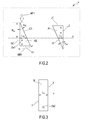
- the translation of the second optical wedge A2 can be obtained by employing a movable structure MT1 supporting the second optical wedge A2 (schematically represented in figure 2 by a dashed arrow) and the rotation of the second optical wedge A2 can be achieved the by means of a rotatable structure MR1 (represented by a dash-dotted arrow) mechanically coupled to the second optical wedge A2.
- the movable structure MT1 is structured to adjust the group delay ⁇ T with a delay increment ⁇ T lower than 10 attoseconds (as).
- the delay increment ⁇ T is lower than 5 as.
- the delay increment ⁇ T is comprised between 0.06 as and 5 as.
- the delay increment ⁇ T is comprised between 0.06 as and 3 as.
- the movable structure MT1 can comprise, as an example, a stepper motor and a servo motor allowing a translation increment of the second optical wedge A2 of 50 nm, so allowing a minimum delay increment ⁇ T of 3 as.
- the movable structure MT1 comprises a translation device based on a stick-slip principle as, for instance, the movement device sold by the company SmarAct GmBH (Germany), which allows a translation increment of the second optical wedge A2 of 1 nm, so allowing a minimum delay increment ⁇ T of 0.06 as.
- the optical element B ( figure 3 ) is made in a second birefringent material, which can be the same first material employed for the first wedge pair 4, and has a second slow polarization direction OX2 parallel to the second direction y, i.e. orthogonal to the first slow polarization direction OX1.
- the optical element B is optically coupled to the first optical wedge pair 4; particularly the first optical wedge pair 4 and the optical element B are separated by free space.
- the second birefringent material can be a uniaxial material or a biaxial optical material.
- the optical element B can be an optical plate having a first input face 7, which is orthogonal to the propagation direction z and faced to the second joining face J2, and an output face 8.
- a first input face 7 which is orthogonal to the propagation direction z and faced to the second joining face J2, and an output face 8.
- the input face 7 and the output face 8 are parallel each other, chromatic dispersion in the radiation passing through the optical element B is avoided, since no refraction phenomena occur when radiation traverses orthogonally face 7 and face 8.
- the delay device 100 can also comprise an optional second adjustable wedge pair device 9 having one optical axis OX3 parallel to the propagation direction z and thus introducing an equal delay in the electromagnetic radiation pulses propagating along the propagation direction z and having linear polarization along the first direction x and the electromagnetic radiation pulses propagating along the propagation direction z and having linear polarization along the second direction y.
- the second adjustable wedge pair device 9 optically coupled to the optical element B, can be analogous to the first adjustable wedge pair 4 and includes a third optical wedge C1 having said optical axis OX3 and a fourth optical wedge C2 having said optical axis OX3.
- the third optical wedge C1 and the fourth optical wedge C2 can be made in a third birefringent material, as an example the first material, and can be a uniaxial or a biaxial optical material.
- the third optical wedge C1 defines a first joining tilted face F1 which is faced to a second joining tilted face F2 of the fourth optical wedge C2.
- the third optical wedge C1 defines a third apex angle ⁇ C1 ( figure 4 ) and the fourth optical wedge C2 defines a fourth apex angle ⁇ C2 .
- the third optical wedge C1 and/or the fourth optical wedge C2 are movable so as to adjust a length of an optical path covered by electromagnetic radiation propagating along the propagation direction z.
- the fourth optical wedge C2 is movable while the third optical wedge C1 is fixed.
- the fourth optical wedge C1 can be translated parallel to the first direction x and/or rotated around an axis parallel to the second direction y.
- the translation of the fourth optical wedge C2 can be obtained by employing a further movable structure MT2, as an example analogous to the movable structure MT1, supporting the fourth optical wedge C2 (schematically represented in figure 4 by a dashed arrow) and the rotation of the fourth optical wedge C2 can be achieved by means of a further rotatable structure MR2 (represented by a dash-dotted arrow) mechanically coupled to the fourth optical wedge C2.
- the delay device 100 is optionally provided with a first output polarizer D ( figure 1 ) structured to project the polarization of incoming radiation along a given direction and provide at an output 10 radiation with a fixed output linear polarization forming an output polarization angle ⁇ P with the first direction x.
- a first output polarizer D figure 1
- ⁇ P output polarization angle
- the delay device 100 illustrated in figure 1 refers to an example in which the employed optical components are optically coupled in free space, i.e. without interposition of further optical components.
- the delay device 100 shows a total geometrical length, computed from the first input 2 to the output 10 along the propagation direction z, comprised between 0.8 - 1.5 cm.
- birefringent materials to be employed in the manufacturing of the first optical wedge pair 4 and/or the optical device B and/or the second optical wedge pair 9
- these materials can be chosen considering the spectral range of the input electromagnetic radiation and the total amount of the delay that the delay device 100 is supposed to introduce.
- employable birefringent materials are: calcite, ⁇ -barium borate ( ⁇ -BBO), magnesium fluoride, crystal quartz, cadmium selenide, cadmium sulphide, cadmium thiogallate and cadmium germanium arsenide.
- the above mentioned materials are "uniaxial birefringent materials”.
- suitable birefringent materials employable for the manufacturing of the Babinet-Soleil module 1 and, as an example, for the second optical wedge pair 9, such as ⁇ -BBO and calcite show a refractive slow index n s comprised between 1.672 and 1.657 and a fast refractive index n f comprised between 1.486 and 1.532.
- an input electromagnetic radiation or beam in the form of the input pulse Pin (shown as an example, in figure 6 ) is provided to the first input 2 of the Babinet - Soleil module 1.
- the input pulse Pin has an input linear polarization forming an angle ⁇ E with the first direction x; in other words, the electric field E associated with the input pulse Pin forms with the first direction x an angle ⁇ E .
- the input pulse Pin has an input linear polarization lying on a plane orthogonal to the propagation direction z and having a direction non-parallel to the first direction x and the second direction y, i.e.: ⁇ E ⁇ n ⁇ ⁇ and ⁇ E ⁇ ⁇ / 2 + n ⁇ ⁇
- the x-component E x travels with group velocity v gs (velocity for the slow direction) and E y travels with group velocity v gf (velocity for the fast direction).
- the x-component E x passes through the first optical pair 4 in time interval or delay T Ax by covering the distance L A1 in the first optical wedge A1 and the distance L A2 in the second optical wedge A2.
- T Ax L A ⁇ 1 + L A ⁇ 2 / v gs
- the y-component E y passes through the first optical pair 4 in another time interval or delay T Ay by covering the distance L A1 in the first optical wedge A1 and the distance L A2 in the second optical wedge A2.
- the time interval T Ax is shorter than the time interval T Ay.
- the movement of the second optical wedge A 2 allows changing the delays T Ax and T Ay , in order to obtain a wished value of the relative delay
- the x-component E x travels with the velocity v gf and the y-component E y travels with velocity v gs .
- the x-component E x passes through the optical element B, covering the distance L B ( figure 3 ), in a propagation time given by a delay T Bx .
- the y-component E y passes through the optical element B, covering the distance L B ( figure 3 ) in a propagation time given by T By .
- the optical element B exchanges the fast and slow polarization directions with respect to the optical wedge pair 4, reversing the relative delay of the pulses.
- Combination of thicknesses of the first and second optical wedges A1, A2 and optical element B allows imparting to the x-component E x and y-component E y any wished negative and positive relative delays.
- the first output pulse P 2x shows a delay T x ' with respect the input pulse Pin which is given by the sum of the delay T Ax of expression (2a) and the delay T Bx of expression (4a):
- the second output pulse P 2y shows a delay T y ' with respect the input pulse Pin which is given by the sum of the delay T Ay of expression (2b) and the delay T By of expression (4b):
- the beam enters the second adjustable wedge pair 9 ( figure 1 ) having the optical axis OX3 ( figure 4 ) parallel to the propagation direction z; in this situation both components E x and E y travel with a corresponding group velocity v g .
- the x-component E x and the y-components E y pass through the second adjustable wedge pair 9 covering a distance L C1 in the third optical wedge C1 and a distance L C2 in the fourth optical wedge C2 and undergoing the same delay T Cx and T Cy :
- Movement of fourth optical wedge C 2 changes by the same amount both delays T Cx and T Cy , but no changes of the relative delay is introduced.
- L tot l A ⁇ 1 + L A ⁇ 2 + L B + L C ⁇ 1 + L C ⁇ 2
- the second adjustable wedge pair 9 can be used to vary the distance L C2 in order to maintain constant the value of the total covered length L tot when an adjustment of the length L A2 has been made to obtain a wished relative delay between the pulses associated with the x-component and the y-component.
- the possibility of keeping at a constant value the total covered length L tot allows to minimize the difference in the total amount of the group velocity dispersion undergone by the x-component E x and the y-components E y passing through the delay device 100. This allows to obtain almost constant group velocity dispersion and pulse duration for different positions of the second optical wedge A2 along the first direction y (at distance M A2 ).
- the possibility of keeping at a constant value the total covered length L tot shows another advantage: it maintains at a constant value the time delay experienced by the propagation through 100 of the pulse having linear polarization along the direction y.
- T 2 T Ay + T
- T Cy L A ⁇ 1 + L A ⁇ 2 / v gf + L B / v gs + L C ⁇ 1 + L C ⁇ 2 / v g
- the second optical wedge pair 9 transmits on its output 10 a first delayed pulse P 1 having, as an example, linear polarization along the first direction x and a second delayed pulse P 2 having, as an example, linear polarization along the second direction y.
- the first delayed pulse P 1 (which can be, as an example, the fastest pulse) exits the second optical wedge pair 9at the delay T 1
- the second delayed pulse P 2 (as an example, the slowest pulse) exits the second optical wedge pair 9at delay T 2 , as shown in figure 8 .
- the beam exiting the second optical wedge 9 enters the output polarizer D which allows the projection of the x-component E x and the y-component E y along the transmission axis P ( Fig. 9 ).
- Fine tuning of the relative group delay ⁇ T can be achieved by moving the second optical wedge A2 and moving accordingly the fourth optical wedge C2 to keep constant the total covered length L tot .
- the second optical wedge A2 and the fourth optical wedge C2 are moved parallel to the first direction x by the same amount ⁇ M.
- the delay device 100 is used, in accordance with particular applications, to dynamically vary the group delay ⁇ T within the above indicated ranges, comprised between the minimum value ⁇ T m and the maximum value ⁇ T M , performing a plurality of adjustments of the group delay according the delay increment ⁇ T.
- the possibility of dynamically scanning a range of values of the group delay ⁇ T is not offered by the Babinet-Soleil compensators in accordance with prior art techniques.
- first optical wedge A1, the second optical wedge A2, the optical element B, the third optical wedge C1 and the fourth optical wedge C2 can be arranged with arbitrary order along the propagation direction z.
- the configurations a), b), c) and d), wherein the first optical wedge pair 4 and the second optical wedge pair 9 are placed in sequence along the propagation of the radiation allow to better adjust the time delays since one single movable structure, such as the first movable structure MT1, of figure 2 , can be employed to move the second optical wedge A2 and the fourth optical wedge C2 by the same amount ⁇ M.
- the second and fourth wedges A2 and C2 can be mounted in optical contact.
- first A1 and second A2 optical wedges are cut so that their slow polarization direction is parallel to the second direction y.
- the slow polarization direction of optical element B is parallel to the first direction x.
- the above described operation of the delay device 100 refers to beams having a finite transverse dimensions d, as an example, comprised between 0.5 mm and 1 cm.
- Figure 10 refers to a second embodiment in which an additional input optical element D0 has been employed in order to obtain an input pulse P in having a linear polarization ⁇ E in accordance with expression (1).
- the input optical element D0 is structured to convert a further input pulse P in ' having linear polarization not complying with expression (1) into the input pulse P in having the required linear polarization.
- the input optical element D0 can be a polarizer, a half-wave plate or a periscope.
- the input element D0 can be also used in any of the embodiments a) to e) above listed and the one of figure 1 .
- the conditions of expression (1) can be fulfilled by suitably rotating the delay device 100 around the propagation direction z.
- the Applicant has performed experiments by manufacturing and testing a delay device analogous to delay device 100 described with reference to figure 1 .
- the first wedge pair 4, the optical element B and the second wedge pair 9 have been realized in ⁇ -barium borate ( ⁇ -BBO).
- the ⁇ -BBO material is a negative uniaxial birefringent optical crystal.
- optical axis is oriented parallel to the second direction y and orthogonal to the first polarization direction OX1 of the first and second optical wedges A1 and A2; the optical axis is parallel to the first direction x and orthogonal to the second polarization direction OX2 of the optical element B; in negative uniaxial birefringent media this corresponds to defining the slow direction of the first and second optical wedges A1 and A2 along direction OX1, and the slow direction of the optical element B along OX2.
- the test was performed using an input pulse P in at a wavelength comprised in the range 500-700 nm.
- the two generated collinear delayed pulses P 1 and P 2 were coupled to a broadband spectrometer to observe spectral interferometry.
- the delayed pulses P 1 and P 2 produced spectral interference fringes, as can be noticed by figures 11a and 11b which show the obtained interference patterns for two different position conditions of the second optical wedge A2 and the fourth optical wedge C2.
- the density of fringes is correlated to the pulses relative delay. From spectral interferometry the following parameters can be measured: the relative pulse delay, the carrier phase and the stability of the relative delay for long experimental time.
- the evolution of the fringe pattern and group delay upon synchronously moving second and fourth wedges A2 and C2 is shown in figure 12 .
- the experimental curve shows the relative delay ⁇ T between the first delayed pulse P 1 and the second delayed pulse P 2 (i.e. the total delay introduced by passing through the delay line 100) versus the glass position, which is the translation M A2 of the second optical wedge A2 by means of the first movable structure MT1 ( figure 2 ).
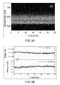
- FIG 13 a shows a sequence of fringe patterns
- figure 13 b) shows the delay between the first pulse P 1 and the second pulse P 2 , and their relative phase deduced from panel 13a) for a static configuration of the experimental set up of the delay device 100.
- the retrieved static fluctuations correspond to less than Tc/360.
- Figure 14 refers to the linear autocorrelation of the pulses exiting the delay device 100.
- figure 14 a) shows the spectrally resolved map
- figure 14 b) shows the intensity trace
- an inset shows the zoom of the trace.
- the inset of Figure 14 b) shows the very high temporal resolution of the delay device 100; it is noted that these data were acquired after moving adjustable distance M A2 with steps of 2 ⁇ m.
- the delay device 100 can introduce delays down to 3.6 as (attosecond).
- the delay device 100 as above described can be manufactured in compact and simple way and the delay between the two pulse replicas is controllable and reproducible over a small fraction of the optical wavelength.
- the two pulses are interferometrically phase locked without need of any active feedback control since there is no path separation that can be affected by thermal fluctuations in the device.
- Such device does not require any costly mechanism that adaptively corrects for delay/phase fluctuations and can be considered as a plug and play device in a standard transient absorption spectroscopy setup.
- FIG 15 shows an embodiment of a two-dimension (2D) spectroscopy system 200 employing a pump-probe geometry.
- the 2D spectroscopy system 200 includes: a first pulse source 201 of the input pulse P in , the phase-locked delay device 100, a second pulse source 202, a sample to be measured 203 in the beams focal plane, a mirror 204 and a spectrometer 205.
- the pump-probe geometry implemented by the system of figure 15 uses the first delayed pulse P 1 and the second delayed pulse P 2 (which are collinear) as the exciting sequence for the sample that is then probed by a third non-collinear pulse P 3 .
- the delay device 100 is particularly suited to generate the interferometrically locked pulses P 1 and P 2 used to excite the sample 203 since it can easily fit in existing pump-probe setups and commercial systems, in which only one pulse is used for excitation.
- the delay device 100 allows an easy and precise scan of the delay ⁇ without changing the T p value since one of the two pulse replicas is not delayed in an absolute temporal frame. The reliability and the sub-optical cycle control are then extremely important for an optimal data elaboration with the Fourier transform over the ⁇ axis. An additional advantage is the possibility to have different polarizations in the exciting pulse sequence as required for some two-dimensional spectroscopy experiments.
- the delay device 100 can also be used in applications concerning the Fourier Transform spectrometer, typically used in the MIR (Medium Infra-Red) spectral region.
- Figure 16 shows schematically a Fourier Transform spectrometer 300 comprising: a further pulse source 301 of the input pulse Pin, the delay device 100 and a detector 302.
- first pulse P 1 and second pulse P 2 collected by detector 302 gives rise to interference traces similar to the one shown in Figure 14(b) .
- Fourier transform of the trace gives the intensity spectrum of the further source 301.
- the detector 302 detects the transmitted energy corresponding to interferometric linear correlation of the first pulse P 1 and second pulse P 12 .
Landscapes
- Physics & Mathematics (AREA)
- Spectroscopy & Molecular Physics (AREA)
- General Physics & Mathematics (AREA)
- Mechanical Light Control Or Optical Switches (AREA)
Abstract
an input port (2) configured to receive an input electromagnetic radiation pulse (Pin); said input pulse being to be propagated along a propagation direction (z) and having a first linear polarization different from both a first direction (x), which is orthogonal to the propagation direction (z), and a second direction (y), which is orthogonal to the first direction (x) and the propagation direction (z);
an adjustable Babinet-Soleil module (1) optically coupled to said input port, having a first polarization direction (OX1) parallel to said first direction (x); wherein the adjustable Babinet-Soleil module is structured to:
provide from the input pulse (Pin) a first pulse (P2x) polarized along the first direction (x) and a second pulse (P2y) collinear to said first pulse and polarized along the second direction (y), and
introduce an adjustable group delay ΔT between the first pulse and the second pulse ranging from a minim value ΔTm and a maximum value ΔTM; the maximum value ΔTM being a value greater than 10 fs.
Description
- This disclosure relates to techniques for generating collinear and phase-locked replicas of an electromagnetic radiation pulse.
- An important application that calls for a pair of phase-locked pulses is the so called Two-dimensional (2D) optical spectroscopy. This technique is used by a growing community of physicists, chemists and biologists both in the infrared (IR) range, targeting vibrational transitions (2DIR spectroscopy), and in the visible range, targeting electronic transitions (2D electronic spectroscopy). In its most simple implementation, 2D spectroscopy uses a pump-probe geometry with two phase-locked collinear pulses exciting the sample, which is then probed by a third non-collinear pulse.
- A second application concerns the FTIR (Fourier Transform infrared) spectrometry. In this technique two delayed broadband beams impinge on a sample in order to measure its absorption spectrum.
- The generation of phase-locked delayed pulse replicas is currently performed by means of two main techniques. The first technique is based on the Michelson interferometer according to which an interference pattern is produced by splitting a beam of light into two paths, bouncing the beams back and recombining them. The Applicant observes that this technique requires complex feedback circuits to keep the interferometer in stability conditions. Moreover, higher feedback accuracy is required for shorter wavelengths; therefore, it is observed that the Michelson interferometer method does not appear satisfying for generating pulse replicas of radiation with sub-wavelength accuracy.
- The generation of delayed pulse replicas by means of a Michelson interferometer is described as an example in M. U. Wehner et al., Opt. Lett. 22, pages 1455-1457 (1997).
- The second known technique is based on a "pulse shaper" which generates the pulse replicas by suitably applying spectral amplitude modulation and spectral phase modulation to a pulse.. This technique appears particularly complex and expensive.
- Document
US-2009-0161092 describes an optical device employed to generate delayed pulse replicas to be employed in a multidimensional spectrometer. - In optics, the Babinet-Soleil compensator is known. The Babinet-Soleil compensator is a continuously variable, zero-order retarder employing a birefringent wedge which is movable and another birefringent wedge which is fixed to a compensator plate. The orientation of the long axis of the wedges is perpendicular to the long axis of the compensator plate. The known Babinet-Soleil compensators are employed in optics to introduce phase delays between two orthogonal polarizations of an electromagnetic field; such phase delays are limited to one optical cycle (e.g. a maximum phase delay of 5.5 fs at 1650 nm) and their effect is to rotate the polarization or act as phase equalizers. Movement of the birefringent wedge is required in order to tune the device to the given electromagnetic field frequency.
- In accordance with an embodiment, a phase-locked delay device comprises:
- an input port configured to receive an input electromagnetic radiation pulse; said input pulse being to be propagated along a propagation direction and having a first linear polarization different from a first direction, which is orthogonal to the propagation direction, and a second direction, which is orthogonal to the first direction and the propagation direction;
- an adjustable Babinet-Soleil module optically coupled to said input port, having a first polarization direction parallel to said first direction, wherein the adjustable Babinet-Soleil module is structured to:
- provide from the input pulse a first pulse polarized along the first direction and a second pulse collinear to said first pulse and polarized along the second direction, and
- introduce an adjustable group delay ΔT between the first pulse and the second pulse ranging from a minim value ΔTm and a maximum value ΔTM; the maximum value ΔTM being a value greater than 10 fs.
- Particular embodiments of the phase-locked delay device are described in the dependent claims 2-12. Claims 13-15 refer to an interferometry system.
- Further characteristics and advantages will be more apparent from the following description of a first embodiment and of its alternatives given as a way of an example with reference to the enclosed drawings in which:
-
Figure 1 schematically shows a first embodiment of a phase-locked delay device; -
Figure 2 schematically shows a lateral view of a first optical wedge pair employable in said phase-locked delay device; -
Figure 3 schematically shows a lateral view of an optical element employable in said phase-locked delay device; -
Figure 4 schematically shows a lateral view of a second optical wedge pair employable in said phase-locked delay device; -
Figure 5 shows a perspective view of an optical wedge employable in said first optical wedge pair; -
Figure 6 shows the shape of an input pulse entering said phase-locked delay device; -
Figure 7 shows an example of linear polarization of the electromagnetic radiation associated with said input pulse; -
Figure 8 shows the shape of two delayed output pulses exiting said phase-locked delay device; -
Figure 9 shows an example of a transmitted linear polarization imposed by an output polarizer included in said phase-locked delay device; -
Figure 10 shows another embodiment of a phase-locked delay device employing an input polarizer; -
Figure 11 shows two interferometry patterns of two pulses obtained with said phase-locked delay device in two different operating conditions; -
Figure 12 shows measured values of the group delay provided by said phase-locked delay device; -
Figure 13 a) shows the evolution of fringe pattern ofFigure 11 (b) andfigure 13 b) refers to the evolution of the group delay and relative phase for a static configuration of the phase-locked delay device; -
Figure 14 refers to linear autocorrelation of a pulse exiting said phase-locked delay device; -
Figure 15 shows an example of practical implementation of a 2D spectroscopy apparatus using said phase-locked delay device; -
Figure 16 shows an example of practical implementation of a FTIR apparatus using said phase-locked delay device. -
Figure 1 shows a first embodiment of a phase-lockeddelay device 100. The phase-locked delay device 100 (hereinafter also "delay device") is configured to generate two delayed, collinear replicas of an input electromagnetic radiation pulse. With reference to the optical structure of thedelay device 100, the following axes/directions can be defined: - a propagation direction z,
- a first direction x, which is orthogonal to the propagation direction z, and
- a second direction y, which is orthogonal to the first direction x and the propagation direction z.
- The first direction x and the second direction y define a plane which is orthogonal to the propagation direction z.
- The
delay device 100 includes an adjustable Babinet-Soleil module 1 which is an optical device comprising optical components in birefringent material/s. - As it is known by the skilled in the art, an electromagnetic field can be always decomposed in the sum of two independent fields with orthogonal polarizations. In a birefringent material the directions of such polarizations are determined by the structure of the material; the two orthogonal directions are named the "fast" and the "slow" polarization directions. The radiation having linear polarization along the fast direction sees the fast refractive index nf and travels with the fast group velocity v gf and the fast phase velocity v pf. The radiation having linear polarization along the slow direction sees the slow refractive index ns and travels with the slow group velocity v gs and the slow phase velocity v ps.
- It is also known by the skilled in the art that birefringence does not occur if the electromagnetic field propagates along one of the two privileged directions of the birefringent material, named "optical axes".
- Birefringent materials are classified "biaxial birefringent materials" when the two optical axes have different orientations in space, and "uniaxial birefringent materials" when the two optical axes degenerate in one axis only.
- The Babinet-Soleil module 1 defines, in accordance with the embodiment described, a first slow polarization direction OX1 parallel to the first direction x and a second slow polarization direction OX2 parallel to second direction y.
- The Babinet-Soleil module 1 is provided with an
input port 2 and an output port 3. Theinput port 2 is structured to receive an electromagnetic radiation input pulse Pin associated with an electromagnetic wave carrier having an optical cycle Tc, wherein Tc = 1/f ; f is the frequency of the electromagnetic wave carrier and f= c/λ, wherein c is the speed of light in vacuum and λ is the wavelength. Therefore the optical cycle Tc is λ/c. - Particularly, the
delay device 100 can be configured to operate on pulses having carrier radiation at wavelength λ comprised at least in the following range: 200 nm - 15000 nm (from the ultraviolet to the mid-infrared range). - The optical cycle Tc of the electromagnetic radiation carrier is comprised between 0.66 femtoseconds (fs) and 50 fs.
- The electromagnetic radiation input pulse Pin (hereinafter also called input pulse) can be an ultra-short pulse and its duration T can be in the femtosecond (fs) to picosecond (ps) range. Such pulses have a broadband optical spectrum, and can be generated by laser systems starting from mode-locked oscillators.
- The Babinet-Soleil module 1 is configured to provide on the first output port 3 and from the input pulse Pin a first output electromagnetic radiation pulse P2x (hereinafter: first output pulse), polarized along the first direction x, and a second electromagnetic radiation pulse P2y (hereinafter: second output pulse) polarized along the second direction y.
- The first output pulse P2x and the second output pulse P2y are collinear, i.e. both pulses propagate along the propagation direction z. The first output pulse P2x and the second output pulse P2y are relatively delayed, i.e. the first output pulse P2x is temporally shifted with respect to the second output pulse P2y.
- The
delay device 100 is designed to introduce an adjustable relative group delay ΔT between the first output pulse P2x and the second output pulse P2y. The group delay ΔT is the delay between the envelopes of the two considered pulses. Thedelay device 100 is designed to allow an adjusting of the group delay ΔT between a minim value ΔTm and a maximum value ΔTM where the maximum value ΔTM is greater than 10 fs. Particularly, the maximum value ΔTM is comprised between 10 fs and 10 ps, and more particularly, is comprised between 10 fs and 4 ps. Moreover, in accordance with particular embodiments the maximum value ΔTM is greater than 100 fs, or is greater than 500 fs. - Particularly, the group delay ΔT can be adjusted to assume values ranging from - 10 ps and + 10 ps; more particularly from -6ps and + 6ps. In accordance with some examples, the group delay ΔT can be adjusted to assume values ranging from - 4ps and + 4 ps or from -2 ps to + 2 ps.
- The design of the
delay device 100 to obtain the above indicated values of the group delay ΔT is based on the choice of suitable birefringent materials, the geometrical arrangement, the accuracy in the positioning of the optical materials, and the wavelength of the electromagnetic field. - It is observed that with the term "phase-locked delay device" it is meant that the device is so as to allow a static control of the relative delay between the two pulses exiting the device itself which shows interferometric precision, that is, as an example, a precision of about Tc/1000, over a long observation time.
- In greater detail and in accordance with the first embodiment, the Babinet-Soleil module 1 comprises a first
adjustable wedge pair 4 and an optical element B. The firstadjustable wedge pair 4 is made of a first birefringent material and structured to introduce a first total shorter delay in radiation having linear polarization along the first slow polarization direction OX1 and a first total longer delay in the radiation having linear polarization along the second direction y. The first birefringent material can be a uniaxial material or a biaxial optical material. - Particularly, the first
adjustable wedge pair 4 comprises a first optical wedge A1 and a second optical wedge A2. Both first A1 and second A2 optical wedges are in the first birefringent material and, as an example, show a first slow polarization direction OX1 parallel to the first direction x and a first fast polarization direction parallel to the second direction y. - As it is clear from
figure 5 , the first optical wedge A1 is an optical prism having a first triangular face S1, a second triangular face S2 parallel to the first triangular face S1 and a first joining face J1, a second joining face J2 and a third joining face J3, each joining parallel sides of the first and second parallel triangular faces S1 and S2. - The first joining face J1, the second joining face J2 and the third joining face J3 are parallelograms which are orthogonal to the first and second triangular faces S1 and S2. The second joining face J2 and the third joining face J3 form a first apex angle αA1 (
figure 2 ) and the second joining face J2 and the first joining face J1 form a right angle. - The second optical wedge A2, analogous to the first optical wedge A1, is an optical prism having a further first triangular face F1, a further second triangular face F2 parallel to the further first triangular face F1 and a further first joining face G1, a further second joining face G2 and a further third joining face G3. The further second joining face G2 and the further third joining face G3 form a second apex angle αA2 (
figure 2 ) and the further second joining face G2 and the further first joining face G1 form a right angle. - According to the first embodiment represented in
figure 1 , the second optical wedge A2 is placed so as to show the further second joining face G2, which acts asfirst input 2, orthogonal to the propagation direction z. The first optical wedge A1 is placed in such a way to show the second joining face J2 orthogonal to the propagation direction z and the third face J3 faced to the further third face G3. The second optical wedge A2 is optically coupled to the first optical wedge A1. - It is observed that the wording "a first optical component is optically coupled to a second optical component" means that electromagnetic radiation can be transmitted from the first optical component to the second optical component and viceversa, and the first optical component and the second optical component can be separated by free space or by a further optical component.
- It is observed that when the first apex angle αA1 is different from the second apex angle αA2 chromatic dispersion is introduced in the radiation passing through the
optical wedge pair 4 since the joining face J3 is not parallel to the joining face G3, and the combination of optical wedge A1 and optical wedge A2 acts as a prism. - The first optical wedge A1 and/or the second optical wedge A2 are movable so as to adjust a length of an optical path covered by radiation along the propagation direction z. According to the first embodiment, the second optical wedge A2 is movable while the first optical wedge A1 is fixed. Particularly, the second optical wedge A2 can be translated parallel to the first direction x and/or rotate around an axis parallel to the second direction y.
- The translation of the second optical wedge A2 can be obtained by employing a movable structure MT1 supporting the second optical wedge A2 (schematically represented in
figure 2 by a dashed arrow) and the rotation of the second optical wedge A2 can be achieved the by means of a rotatable structure MR1 (represented by a dash-dotted arrow) mechanically coupled to the second optical wedge A2. - In accordance with the described embodiment, the movable structure MT1 is structured to adjust the group delay ΔT with a delay increment δT lower than 10 attoseconds (as). Particularly, the delay increment δT is lower than 5 as. More particularly, the delay increment δT is comprised between 0.06 as and 5 as. In accordance with an example, the delay increment δT is comprised between 0.06 as and 3 as.
- The movable structure MT1 can comprise, as an example, a stepper motor and a servo motor allowing a translation increment of the second optical wedge A2 of 50 nm, so allowing a minimum delay increment δT of 3 as. In accordance with another example, the movable structure MT1 comprises a translation device based on a stick-slip principle as, for instance, the movement device sold by the company SmarAct GmBH (Germany), which allows a translation increment of the second optical wedge A2 of 1 nm, so allowing a minimum delay increment δT of 0.06 as.
- The optical element B (
figure 3 ) is made in a second birefringent material, which can be the same first material employed for thefirst wedge pair 4, and has a second slow polarization direction OX2 parallel to the second direction y, i.e. orthogonal to the first slow polarization direction OX1. The optical element B is optically coupled to the firstoptical wedge pair 4; particularly the firstoptical wedge pair 4 and the optical element B are separated by free space. The second birefringent material can be a uniaxial material or a biaxial optical material. - The optical element B can be an optical plate having a first input face 7, which is orthogonal to the propagation direction z and faced to the second joining face J2, and an
output face 8. In the case in which the input face 7 and theoutput face 8 are parallel each other, chromatic dispersion in the radiation passing through the optical element B is avoided, since no refraction phenomena occur when radiation traverses orthogonally face 7 andface 8. - In accordance with the first embodiment the
delay device 100 can also comprise an optional second adjustablewedge pair device 9 having one optical axis OX3 parallel to the propagation direction z and thus introducing an equal delay in the electromagnetic radiation pulses propagating along the propagation direction z and having linear polarization along the first direction x and the electromagnetic radiation pulses propagating along the propagation direction z and having linear polarization along the second direction y. - The second adjustable
wedge pair device 9, optically coupled to the optical element B, can be analogous to the firstadjustable wedge pair 4 and includes a third optical wedge C1 having said optical axis OX3 and a fourth optical wedge C2 having said optical axis OX3. - The third optical wedge C1 and the fourth optical wedge C2 can be made in a third birefringent material, as an example the first material, and can be a uniaxial or a biaxial optical material.
- The third optical wedge C1 defines a first joining tilted face F1 which is faced to a second joining tilted face F2 of the fourth optical wedge C2. The third optical wedge C1 defines a third apex angle αC1 (
figure 4 ) and the fourth optical wedge C2 defines a fourth apex angle αC2. - The third optical wedge C1 and/or the fourth optical wedge C2 are movable so as to adjust a length of an optical path covered by electromagnetic radiation propagating along the propagation direction z. According to the first embodiment, the fourth optical wedge C2 is movable while the third optical wedge C1 is fixed. Particularly, the fourth optical wedge C1 can be translated parallel to the first direction x and/or rotated around an axis parallel to the second direction y.
- The translation of the fourth optical wedge C2 can be obtained by employing a further movable structure MT2, as an example analogous to the movable structure MT1, supporting the fourth optical wedge C2 (schematically represented in
figure 4 by a dashed arrow) and the rotation of the fourth optical wedge C2 can be achieved by means of a further rotatable structure MR2 (represented by a dash-dotted arrow) mechanically coupled to the fourth optical wedge C2. - The
delay device 100 is optionally provided with a first output polarizer D (figure 1 ) structured to project the polarization of incoming radiation along a given direction and provide at anoutput 10 radiation with a fixed output linear polarization forming an output polarization angle ϕP with the first direction x. - The
delay device 100 illustrated infigure 1 refers to an example in which the employed optical components are optically coupled in free space, i.e. without interposition of further optical components. - As an example, the
delay device 100 shows a total geometrical length, computed from thefirst input 2 to theoutput 10 along the propagation direction z, comprised between 0.8 - 1.5 cm. - With reference to the selection of materials (particularly, birefringent materials) to be employed in the manufacturing of the first
optical wedge pair 4 and/or the optical device B and/or the secondoptical wedge pair 9, these materials can be chosen considering the spectral range of the input electromagnetic radiation and the total amount of the delay that thedelay device 100 is supposed to introduce. Examples of employable birefringent materials are: calcite, α-barium borate (α-BBO), magnesium fluoride, crystal quartz, cadmium selenide, cadmium sulphide, cadmium thiogallate and cadmium germanium arsenide. The above mentioned materials are "uniaxial birefringent materials". - Moreover, it is noticed that suitable birefringent materials employable for the manufacturing of the Babinet-Soleil module 1 and, as an example, for the second
optical wedge pair 9, such as α-BBO and calcite show a refractive slow index ns comprised between 1.672 and 1.657 and a fast refractive index nf comprised between 1.486 and 1.532. - With reference to the operation of the
delay device 100 offigure 1 , an input electromagnetic radiation or beam in the form of the input pulse Pin (shown as an example, infigure 6 ) is provided to thefirst input 2 of the Babinet - Soleil module 1. - As shown in
figure 7 , the input pulse Pin has an input linear polarization forming an angle ϕE with the first direction x; in other words, the electric field E associated with the input pulse Pin forms with the first direction x an angle ϕE. The input pulse Pin has an input linear polarization lying on a plane orthogonal to the propagation direction z and having a direction non-parallel to the first direction x and the second direction y, i.e.:
- The first input beam Pin enters the second optical wedge A2 and its projection along the first direction x and the second direction y gives an x-component of the electrical field Ex and an y-component of the electrical field Eycalculated as follows:


- Since the first slow polarization direction OX1 of the first and second optical wedges A1 and A2 is along the first direction x, the x-component Ex travels with group velocity vgs (velocity for the slow direction) and Ey travels with group velocity vgf (velocity for the fast direction). The x-component Ex passes through the first
optical pair 4 in time interval or delay TAx by covering the distance LA1 in the first optical wedge A1 and the distance LA2 in the second optical wedge A2. - The time interval or delay TAx for the x-component Ex is given by the following expression:

- The y-component Ey passes through the first
optical pair 4 in another time interval or delay TAy by covering the distance LA1 in the first optical wedge A1 and the distance LA2 in the second optical wedge A2. The delay TAy is given by the following expression:
- vgs<vgf, therefore the time interval TAx is shorter than the time interval TAy.
- It is observed that the movable structure MT1 (
figure 2 ) moves the second optical wedge A2 by an adjustable distance MA2 along the first direction x; the distance LA2 to be covered by the beam depends on the adjustable distance MA2 according to equation:
- Therefore, the movement of the second optical wedge A2 allows changing the delays TAx and TAy , in order to obtain a wished value of the relative delay | TAx - TAy |.
- The beam exiting the first
optical wedge pair 4, under the form of two delayed pulses, enters the optical element B, which has the second slow polarization direction OX2 parallel to the second direction y. Hence, the x-component Ex travels with the velocity vgf and the y-component Ey travels with velocity vgs. - The x-component Ex passes through the optical element B, covering the distance LB (
figure 3 ), in a propagation time given by a delay TBx .. The delay TBx for the x-component Ex is given by the following expression:
- The y-component Ey passes through the optical element B, covering the distance LB (
figure 3 ) in a propagation time given by TBy. The delay TBy for the y-component Ey is given by the following expression:
- As clear from a comparison with equations (2a) and (2b), the optical element B exchanges the fast and slow polarization directions with respect to the
optical wedge pair 4, reversing the relative delay of the pulses. The relative delay T0 between the y-component Ey and the x-component Ex is:
- The delay T0 defines a fixed delay between the pulses. As an example, if element B has thickness LB = 0, then T0 = 0.
- Combination of thicknesses of the first and second optical wedges A1, A2 and optical element B allows imparting to the x-component Ex and y-component Ey any wished negative and positive relative delays.
- At the output of Babinet-Soleil module 1, the first output pulse P2x shows a delay Tx' with respect the input pulse Pin which is given by the sum of the delay TAx of expression (2a) and the delay TBx of expression (4a):

- With reference to the y-component, at the output of the Babinet-Soleil module 1, the second output pulse P2y shows a delay Ty' with respect the input pulse Pin which is given by the sum of the delay TAy of expression (2b) and the delay TBy of expression (4b):

- The beam enters the second adjustable wedge pair 9 (
figure 1 ) having the optical axis OX3 (figure 4 ) parallel to the propagation direction z; in this situation both components Ex and Ey travel with a corresponding group velocity vg . The x-component Ex and the y-components Ey pass through the secondadjustable wedge pair 9 covering a distance LC1 in the third optical wedge C1 and a distance LC2 in the fourth optical wedge C2 and undergoing the same delay TCx and TCy :
- It is observed that the further movable structure MT2 (
figure 4 ) can be used to move the fourth optical wedge C2 by an adjustable distance MC2 along the first direction x; the distance LC2 to be covered by the beam depends on the adjustable distance MC2 according to equation:
- Movement of fourth optical wedge C2 changes by the same amount both delays TCx and TCy , but no changes of the relative delay is introduced.
- The total distance Ltot covered by the beam in passing through the Babinet-Soleil module 1 and the second
optical wedge pair 9 is given by the expression:
- In expression (9) the distance covered in free space propagation between the optical elements has been not included since it is not affecting the relative delay between the two pulses.
- It is observed that the second
adjustable wedge pair 9 can be used to vary the distance LC2 in order to maintain constant the value of the total covered length Ltot when an adjustment of the length LA2 has been made to obtain a wished relative delay between the pulses associated with the x-component and the y-component. - The possibility of keeping at a constant value the total covered length Ltot allows to minimize the difference in the total amount of the group velocity dispersion undergone by the x-component Ex and the y-components Ey passing through the
delay device 100. This allows to obtain almost constant group velocity dispersion and pulse duration for different positions of the second optical wedge A2 along the first direction y (at distance MA2). - Moreover, the possibility of keeping at a constant value the total covered length Ltot shows another advantage: it maintains at a constant value the time delay experienced by the propagation through 100 of the pulse having linear polarization along the direction y.
- The propagation through the Babinet-Soleil module 1 and the second
optical wedge 9 imparts to components Ex and Ey the following total delays T1 and T2 :

- The second
optical wedge pair 9 transmits on its output 10 a first delayed pulse P1 having, as an example, linear polarization along the first direction x and a second delayed pulse P2 having, as an example, linear polarization along the second direction y. - The first delayed pulse P1 (which can be, as an example, the fastest pulse) exits the second optical wedge pair 9at the delay T1 , the second delayed pulse P2 (as an example, the slowest pulse) exits the second optical wedge pair 9at delay T2 , as shown in
figure 8 . The relative group delay ΔT is ΔT = T2 - T1. - As an example, considering the distance LA1 +LA2 = 1.3 mm and LB = 1.6 mm, if the group velocities vgo and vge have the values 1.7544x10⁸ m/s and 1.9229x10⁸ m/s, the relative group delay is ΔT = 150 fs.
- If the input pulse Pin has intensity Iin, the first delayed pulse P1 and the second delayed pulse P2 have intensities:


- The beam exiting the second
optical wedge 9 enters the output polarizer D which allows the projection of the x-component Ex and the y-component Ey along the transmission axis P (Fig. 9 ). The intensities I(x)out and I(y)out of the x-component Ex and the y-component Ey after the output polarizer D are:

- Fine tuning of the relative group delay ΔT can be achieved by moving the second optical wedge A2 and moving accordingly the fourth optical wedge C2 to keep constant the total covered length Ltot.
- According to the considered example, the second optical wedge A2 and the fourth optical wedge C2 are moved parallel to the first direction x by the same amount ΔM. The distance covered by the beam in the second optical wedge A2 is given by the formula:

- The distance covered by the beam in the fourth optical wedge C2 is given by the formula:

- The delays Tx and Ty of expressions (10a) and (10b) become the delays Tx " and Ty" :

- It is observed from eq. (14b) that when α A2 = α C2 and vgf = vg, then Ty" = Ty = constant: the y-component Ey exhibits a delay which does not change when the second optical wedge A2 and the fourth optical wedge C2 are moved by the same amount ΔM.
- It is noted that when fabrication errors cause α A2 ≠ α C2 and/or when vgf ≠ vg the device is equipped to keep Ty constant: the systematic error can be compensated for by rotating the optical wedge with the smaller apex angle by means of the rotatable structure MR1 and the further rotatable structure MR2.
- When αA2 = αC2 and vgf = vg (or equivalently rotation is applied to one of the wedges), the delays are:


- Relative group delay ΔT is therefore:

- Therefore, fine regulation of the relative delay of the order of ΔM·tan(α A2 ) · [1/vgs - 1/vgf ] can be obtained. As an example, for apex angles of 7° and ΔM of 0.1 micrometers, relative delays of the order of 6 as can be obtained. The Applicants observe that the known Babinet-Soleil compensators are not designed and used to obtain the above mentioned maximum values ΔTM of the group delay ΔT which are obtainable with the described
delay device 100. - Moreover, it's also noticed that the
delay device 100 is used, in accordance with particular applications, to dynamically vary the group delay ΔT within the above indicated ranges, comprised between the minimum value ΔTm and the maximum value ΔTM, performing a plurality of adjustments of the group delay according the delay increment δT. The possibility of dynamically scanning a range of values of the group delay ΔT is not offered by the Babinet-Soleil compensators in accordance with prior art techniques. - It is noted that in accordance with further embodiments the first optical wedge A1, the second optical wedge A2, the optical element B, the third optical wedge C1 and the fourth optical wedge C2 can be arranged with arbitrary order along the propagation direction z.
- Particularly, the following further configurations are possible along the propagation direction z, wherein the output polarizer D is kept as the last component of the line:
- a) first
optical wedge pair 4, secondoptical wedge pair 9 and optical element B; - b) second
optical wedge pair 9, firstoptical wedge pair 4, optical element B; - c) optical component B, first
optical wedge pair 4, secondoptical wedge pair 9; - d) optical element B, second
optical wedge pair 9, firstoptical wedge pair 4; - e) second
optical wedge pair 9, optical element B, firstoptical wedge pair 4. - Particularly, the configurations a), b), c) and d), wherein the first
optical wedge pair 4 and the secondoptical wedge pair 9 are placed in sequence along the propagation of the radiation, allow to better adjust the time delays since one single movable structure, such as the first movable structure MT1, offigure 2 , can be employed to move the second optical wedge A2 and the fourth optical wedge C2 by the same amount ΔM. In addition, in configurations b) and d), the second and fourth wedges A2 and C2 can be mounted in optical contact. - In a further embodiment, the first A1 and second A2 optical wedges are cut so that their slow polarization direction is parallel to the second direction y. In this case, the slow polarization direction of optical element B is parallel to the first direction x.
- It is also observed that the above described operation of the
delay device 100 refers to beams having a finite transverse dimensions d, as an example, comprised between 0.5 mm and 1 cm. -
Figure 10 refers to a second embodiment in which an additional input optical element D0 has been employed in order to obtain an input pulse Pin having a linear polarization ϕE in accordance with expression (1). The input optical element D0 is structured to convert a further input pulse Pin' having linear polarization not complying with expression (1) into the input pulse Pin having the required linear polarization. The input optical element D0 can be a polarizer, a half-wave plate or a periscope. The input element D0 can be also used in any of the embodiments a) to e) above listed and the one offigure 1 . - According to another technique, the conditions of expression (1) can be fulfilled by suitably rotating the
delay device 100 around the propagation direction z. - The Applicant has performed experiments by manufacturing and testing a delay device analogous to delay
device 100 described with reference tofigure 1 . Thefirst wedge pair 4, the optical element B and thesecond wedge pair 9 have been realized in α-barium borate (α-BBO). The α-BBO material is a negative uniaxial birefringent optical crystal. Its optical axis is oriented parallel to the second direction y and orthogonal to the first polarization direction OX1 of the first and second optical wedges A1 and A2; the optical axis is parallel to the first direction x and orthogonal to the second polarization direction OX2 of the optical element B; in negative uniaxial birefringent media this corresponds to defining the slow direction of the first and second optical wedges A1 and A2 along direction OX1, and the slow direction of the optical element B along OX2. The optical axis of the third and fourth optical wedges C1 and C2 is oriented along the optical axis OX3, thus giving vgf = vg . - The above defined apex angles αA1, αA2, αC1, αC2 were equal to 7°: αA1 = αA2 = αC1 = αC2 = 7°.
- The angles defining the linear polarizations of the input pulse Pin and the delayed pulses P1 and P2 were ϕE = ϕP = 45°. The test was performed using an input pulse Pin at a wavelength comprised in the range 500-700 nm.
- The two generated collinear delayed pulses P1 and P2 were coupled to a broadband spectrometer to observe spectral interferometry. The delayed pulses P1 and P2 produced spectral interference fringes, as can be noticed by
figures 11a and 11b which show the obtained interference patterns for two different position conditions of the second optical wedge A2 and the fourth optical wedge C2. - The density of fringes is correlated to the pulses relative delay. From spectral interferometry the following parameters can be measured: the relative pulse delay, the carrier phase and the stability of the relative delay for long experimental time.
- The evolution of the fringe pattern and group delay upon synchronously moving second and fourth wedges A2 and C2 is shown in
figure 12 . The experimental curve shows the relative delay ΔT between the first delayed pulse P1 and the second delayed pulse P2 (i.e. the total delay introduced by passing through the delay line 100) versus the glass position, which is the translation MA2 of the second optical wedge A2 by means of the first movable structure MT1 (figure 2 ). - This result is in very good agreement with the delays calculated from the dispersion equations of α-BBO.
- The stability behaviour of the relative delay for a fixed position of wedges is shown in
figure 13. Figure 13 a) shows a sequence of fringe patterns;figure 13 b) shows the delay between the first pulse P1 and the second pulse P2, and their relative phase deduced from panel 13a) for a static configuration of the experimental set up of thedelay device 100. The retrieved static fluctuations correspond to less than Tc/360. -
Figure 14 refers to the linear autocorrelation of the pulses exiting thedelay device 100. In greater details,figure 14 a) shows the spectrally resolved map;figure 14 b) shows the intensity trace and an inset shows the zoom of the trace. - The inset of
Figure 14 b) shows the very high temporal resolution of thedelay device 100; it is noted that these data were acquired after moving adjustable distance MA2 with steps of 2 µm. With a first movable structure MT1 with 0.1 µm maximum resolution, thedelay device 100 can introduce delays down to 3.6 as (attosecond). - It is observed that the
delay device 100 as above described can be manufactured in compact and simple way and the delay between the two pulse replicas is controllable and reproducible over a small fraction of the optical wavelength. - Moreover, it is noticed that the two pulses are interferometrically phase locked without need of any active feedback control since there is no path separation that can be affected by thermal fluctuations in the device. Such device does not require any costly mechanism that adaptively corrects for delay/phase fluctuations and can be considered as a plug and play device in a standard transient absorption spectroscopy setup.
- In addition, it can be employed in various spectral ranges without any limitation.
-
Figure 15 shows an embodiment of a two-dimension (2D) spectroscopy system 200 employing a pump-probe geometry. The 2D spectroscopy system 200 includes: afirst pulse source 201 of the input pulse Pin, the phase-lockeddelay device 100, asecond pulse source 202, a sample to be measured 203 in the beams focal plane, amirror 204 and aspectrometer 205. - In particular, the pump-probe geometry implemented by the system of
figure 15 uses the first delayed pulse P1 and the second delayed pulse P2 (which are collinear) as the exciting sequence for the sample that is then probed by a third non-collinear pulse P3. Thespectrometer 205 measures the transient changes induced by the pulse pair P1 and P2 as a function of their delay ΔT = τ at a fixed delay Tp. - It is observed that an interferometric stability is required since a Fourier transform has to be operated over the time trace obtained by scanning the relative delay ΔT = τ between the first delayed pulse P1 and the second delayed pulse P2. In fact, these pulses will build up a nonlinear polarization oscillating with the optical cycle period thus requiring a high control of the optical delay with the relative pulse carriers jittering less than λ/100.
- The
delay device 100 is particularly suited to generate the interferometrically locked pulses P1 and P2 used to excite thesample 203 since it can easily fit in existing pump-probe setups and commercial systems, in which only one pulse is used for excitation. - The
delay device 100 allows an easy and precise scan of the delay τ without changing the Tp value since one of the two pulse replicas is not delayed in an absolute temporal frame. The reliability and the sub-optical cycle control are then extremely important for an optimal data elaboration with the Fourier transform over the τ axis. An additional advantage is the possibility to have different polarizations in the exciting pulse sequence as required for some two-dimensional spectroscopy experiments. - The
delay device 100 can also be used in applications concerning the Fourier Transform spectrometer, typically used in the MIR (Medium Infra-Red) spectral region.Figure 16 shows schematically a Fourier Transform spectrometer 300 comprising: afurther pulse source 301 of the input pulse Pin, thedelay device 100 and adetector 302. - At various delays τ, light from first pulse P1 and second pulse P2 collected by
detector 302 gives rise to interference traces similar to the one shown inFigure 14(b) . Fourier transform of the trace gives the intensity spectrum of thefurther source 301. Thedetector 302 detects the transmitted energy corresponding to interferometric linear correlation of the first pulse P1 and second pulse P12.
Claims (15)
- A phase-locked delay device (100), comprising:an input port (2) configured to receive an input electromagnetic radiation pulse (Pin); said input pulse being to be propagated along a propagation direction (z) and having a first linear polarization different from both a first direction (x), which is orthogonal to the propagation direction (z), and a second direction (y), which is orthogonal to the first direction (x) and the propagation direction (z);an adjustable Babinet-Soleil module (1) optically coupled to said input port, having a first polarization direction (OX1) parallel to said first direction (x); wherein the adjustable Babinet-Soleil module is structured to:provide from the input pulse (Pin) a first pulse (P2x) polarized along the first direction (x) and a second pulse (P2y) collinear to said first pulse and polarized along the second direction (y), andintroduce an adjustable group delay ΔT between the first pulse and the second pulse ranging from a minim value ΔTm and a maximum value ΔTM; the maximum value ΔTM being a value greater than 10 fs.
- The delay device of claim 1, wherein the maximum value ΔTM is comprised between 10 fs and 10 ps; preferably, the maximum value ΔTM is comprised between 10 fs and 4 ps; more preferably, the maximum value ΔTM is comprised between 100 fs and 4 ps.
- The delay device of claim 1, wherein the device (100) is structured to adjust the group delay ΔT to assume values between -4ps and +4ps.
- The delay device of claim 1, wherein the Babinet-Soleil module is structured to adjust the group delay ΔT with an increment δT lower than 10 as; preferably, the Babinet-Soleil module is structured to adjust the group delay ΔT with an increment δT lower than 5 as.
- The delay device of claim 1, further including: an input polarizer (Do) having an output coupled to said input port (2) and structured to receive an electromagnetic radiation pulse having a second polarization different from said first linear polarization and convert the electromagnetic radiation pulse into said input pulse (Pin).
- The delay device of claim 1, wherein said first linear polarization forms an angle of 45° with the first direction and the second direction.
- The delay device of claim 1, wherein the Babinet-Soleil module (A1, A2, B) includes:a first adjustable wedge pair (A1, A2) in a first birefringent material structured to introduce a first total shorter delay in the first pulse and a first total longer delay in the second pulse;an optical element (B) in a second birefringent material structured to introduce a longer delay in the first pulse and a shorter delay in the second pulse;wherein the first adjustable wedge pair includes:a first optical wedge (A2) in the first birefringent material defining a first wedge-surface (G2), having the first polarization direction (OX1) and structured to introduce a first shorter delay in the first pulse and a first longer delay in the second pulse;a second optical wedge (A1) in the first birefringent material having said first polarization direction, defining a second wedge-surface faced to said first wedge-surface and configured to introduce a second shorter delay in the first pulse and a second longer delay in the second pulse ; at least one between the first and second optical wedges being movable to vary a length of an optical path along the propagation direction.
- The delay device of claim 7, further including:a second adjustable wedge pair (C1, C2) in a third material optically coupled to the Babinet-Soleil module 1, structured to have an optical axis parallel (OX3) to said propagation direction (z) and introduce an equal delay in electromagnetic radiation pulses propagating along the third optical axis; the second adjustable wedge pair being configured to be movable to vary an optical path along the propagation direction so as to keep at a constant value a total length covered by electromagnetic radiation in passing through the phase-locked delay device.wherein the second adjustable wedge pair (C1, C2) is placed in one of the following positions along the propagation direction (z): between the input (2) and the first adjustable wedge pair (A1, A2); between the first adjustable wedge pair (A1, A2) and the first optical element (B).
- The delay device of claim 8, wherein said optical element (B) is placed before the first wedge pair (A1, A2) according to the propagation direction of the radiation.
- The delay device of claim 8, wherein said second adjustable wedge pair (C1,C2) includes:a third optical wedge (C1) having said optical axis, defining a third wedge-surface and structured to introduce a first delay in said electromagnetic radiation pulses;a fourth optical wedge (C2) having said optical axis, defining a fourth wedge-surface faced to said third wedge-surface and configured to introduce a second delay in said electromagnetic radiation pulses; at least one between the first and second optical wedges being movable to vary said further optical path along the propagation direction.
- The delay device of claim 8, wherein the first, the second and the third materials are made in at least one of the following materials: uniaxial birefringent material, biaxial birefringent material.
- The delay device of claim 8, further comprising:a first movable structure (MT1) supporting at least one of said first and second optical wedges to adjust radiation delays,a second movable structure (MT2) supporting at least one of said third and fourth optical wedges to further adjust radiation delays.a further movable structure supporting at least one of said first and second optical wedges and at least one of said third and fourth optical wedges.
- Interferometry system (200; 300) comprising:a first pulse source (201, 301) configured to generate an input electromagnetic radiation pulse (Pin) to be propagated along a propagation direction (z) and having a first linear polarization different from a first direction (x), which is orthogonal to the propagation direction (z), and a second direction (y), which is orthogonal to the first direction (x) and the propagation direction (z);an input port (2) configured to receive the input pulse (Pin);an adjustable Babinet-Soleil module (1) optically coupled to said input port, having a first polarization direction (OX1) parallel to said first direction (x); wherein the adjustable Babinet-Soleil module is structured to:provide from the input pulse (Pin) a first pulse (P2x) polarized along the first direction (x) and a second pulse (P2y) collinear to said first pulse and polarized along the second direction (y), andintroduce an adjustable group delay ΔT between the first pulse and the second pulse ranging from a minim value ΔTm and a maximum value ΔTM; the maximum value ΔTM being a value greater than 10 fs;an apparatus structured to analyze a interferometry beam obtained from said first and second pulses.
- The interferometry system of claim 13, wherein said system is a two-dimension spectroscopy system and said apparatus includes:a second pulse source (202) configured to emit a second input pulse (P3),a sample (203) to be measured by the two-dimensional spectroscopy system configured to receive the first pulse, the second pulse and the second input pulse and provide for an output beam;spectrometer (205) structured to receive and analyze the output beam.
- The interferometry system of claim 13, wherein said system is a Fourier Transform spectrometer and said apparatus includes:a detector for detecting transmitted energy corresponding to interferometric linear correlation of said first pulse and second pulse.
Applications Claiming Priority (1)
| Application Number | Priority Date | Filing Date | Title |
|---|---|---|---|
| US13/490,862 US9182284B2 (en) | 2012-06-07 | 2012-06-07 | Phase-locked delay device including an optical wedge pair |
Publications (2)
| Publication Number | Publication Date |
|---|---|
| EP2672244A1 true EP2672244A1 (en) | 2013-12-11 |
| EP2672244B1 EP2672244B1 (en) | 2021-07-14 |
Family
ID=48537775
Family Applications (1)
| Application Number | Title | Priority Date | Filing Date |
|---|---|---|---|
| EP13168800.4A Active EP2672244B1 (en) | 2012-06-07 | 2013-05-22 | Phase-locked delay device including two optical wedge pairs |
Country Status (2)
| Country | Link |
|---|---|
| US (1) | US9182284B2 (en) |
| EP (1) | EP2672244B1 (en) |
Cited By (3)
| Publication number | Priority date | Publication date | Assignee | Title |
|---|---|---|---|---|
| CN107907980A (en) * | 2017-12-06 | 2018-04-13 | 南京大学 | A kind of interferometer |
| WO2023160924A1 (en) * | 2022-02-22 | 2023-08-31 | Asml Netherlands B.V. | Method and apparatus for reflecting pulsed radiation |
| CN117233108A (en) * | 2022-06-06 | 2023-12-15 | 中国科学院大连化学物理研究所 | A high-throughput nanosecond transient absorption spectrum measurement system and method |
Families Citing this family (5)
| Publication number | Priority date | Publication date | Assignee | Title |
|---|---|---|---|---|
| CN109506793A (en) * | 2019-01-16 | 2019-03-22 | 中国工程物理研究院激光聚变研究中心 | A kind of single-shot time femto-second laser pulse waveform meter |
| CN109682484A (en) * | 2019-02-01 | 2019-04-26 | 中国工程物理研究院激光聚变研究中心 | A kind of single-shot time femto-second laser pulse waveform meter |
| CN109682483A (en) * | 2019-02-01 | 2019-04-26 | 中国工程物理研究院激光聚变研究中心 | A kind of single-shot time Ps Laser Pulse waveform meter |
| JPWO2024185522A1 (en) * | 2023-03-03 | 2024-09-12 | ||
| IT202300005346A1 (en) | 2023-03-21 | 2024-09-21 | Nireos S R L | INTERFEROMETRIC APPARATUS |
Citations (3)
| Publication number | Priority date | Publication date | Assignee | Title |
|---|---|---|---|---|
| US6195167B1 (en) * | 1997-08-19 | 2001-02-27 | The University Court Of The University Of St. Andrews | Autocorrelation of ultrashort electromagnetic pulses |
| US20080175597A1 (en) * | 2007-01-24 | 2008-07-24 | Oki Electric Industry Co., Ltd. | Optical clock signal regeneration device |
| US20090161092A1 (en) | 2007-12-21 | 2009-06-25 | Martin Thomas Zanni | Multidimensional spectrometer |
Family Cites Families (3)
| Publication number | Priority date | Publication date | Assignee | Title |
|---|---|---|---|---|
| US3737235A (en) * | 1972-02-10 | 1973-06-05 | Cary Instruments | Polarization interferometer with beam polarizing compensator |
| JPH05232384A (en) * | 1992-02-18 | 1993-09-10 | Olympus Optical Co Ltd | Interference microscope |
| US8526002B2 (en) * | 2007-09-07 | 2013-09-03 | Massachusetts Institute Of Technology | Two-dimensional fourier transform spectrometer |
-
2012
- 2012-06-07 US US13/490,862 patent/US9182284B2/en active Active
-
2013
- 2013-05-22 EP EP13168800.4A patent/EP2672244B1/en active Active
Patent Citations (3)
| Publication number | Priority date | Publication date | Assignee | Title |
|---|---|---|---|---|
| US6195167B1 (en) * | 1997-08-19 | 2001-02-27 | The University Court Of The University Of St. Andrews | Autocorrelation of ultrashort electromagnetic pulses |
| US20080175597A1 (en) * | 2007-01-24 | 2008-07-24 | Oki Electric Industry Co., Ltd. | Optical clock signal regeneration device |
| US20090161092A1 (en) | 2007-12-21 | 2009-06-25 | Martin Thomas Zanni | Multidimensional spectrometer |
Non-Patent Citations (4)
| Title |
|---|
| M. U. WEHNER ET AL., OPT. LETT., vol. 22, 1997, pages 1455 - 1457 |
| PAWLOWSKA MONIKA ET AL: "Collinear interferometer with variable delay for carrier-envelope offset frequency measurement", REVIEW OF SCIENTIFIC INSTRUMENTS, AIP, MELVILLE, NY, US, vol. 80, no. 8, 18 August 2009 (2009-08-18), pages 83101 - 83101, XP012128427, ISSN: 0034-6748, DOI: 10.1063/1.3197404 * |
| POCHI YEH: "Autocorrelation of ultrashort optical pulses using polarization interferometry", OPTICS LETTERS, vol. 8, no. 6, 1 June 1983 (1983-06-01), pages 330, XP055073975, ISSN: 0146-9592, DOI: 10.1364/OL.8.000330 * |
| WEHNER M U ET AL: "SCANNING INTERFEROMETER STABILIZED BY USE OF PANCHARATNAM'S PHASE", OPTICS LETTERS, OSA, OPTICAL SOCIETY OF AMERICA, WASHINGTON, DC, US, vol. 22, no. 19, 1 October 1997 (1997-10-01), pages 1455 - 1457, XP000723619, ISSN: 0146-9592 * |
Cited By (4)
| Publication number | Priority date | Publication date | Assignee | Title |
|---|---|---|---|---|
| CN107907980A (en) * | 2017-12-06 | 2018-04-13 | 南京大学 | A kind of interferometer |
| CN107907980B (en) * | 2017-12-06 | 2019-04-23 | 南京大学 | an interferometer |
| WO2023160924A1 (en) * | 2022-02-22 | 2023-08-31 | Asml Netherlands B.V. | Method and apparatus for reflecting pulsed radiation |
| CN117233108A (en) * | 2022-06-06 | 2023-12-15 | 中国科学院大连化学物理研究所 | A high-throughput nanosecond transient absorption spectrum measurement system and method |
Also Published As
| Publication number | Publication date |
|---|---|
| EP2672244B1 (en) | 2021-07-14 |
| US9182284B2 (en) | 2015-11-10 |
| US20130329228A1 (en) | 2013-12-12 |
Similar Documents
| Publication | Publication Date | Title |
|---|---|---|
| EP2672244B1 (en) | Phase-locked delay device including two optical wedge pairs | |
| Réhault et al. | Two-dimensional electronic spectroscopy with birefringent wedges | |
| Manzoni et al. | Coherent pulse synthesis: towards sub‐cycle optical waveforms | |
| Köhler et al. | Zeptosecond precision pulse shaping | |
| JP6134773B2 (en) | Optical resonator device and method for adjusting round-trip time in resonator | |
| US7760342B2 (en) | Multidimensional spectrometer | |
| US11205883B2 (en) | Dispersion adjustment units and methods of use | |
| US8665446B2 (en) | Apparatus and method for coherent multi-dimensional optical spectroscopy | |
| Réhault et al. | 2D IR spectroscopy with phase-locked pulse pairs from a birefringent delay line | |
| CN110687093B (en) | Dual-frequency CARS measuring device and method based on bound-state optical solitons | |
| US10317774B2 (en) | All optical sampling by slanted light interrogation for cross-correlated encoded recording (slicer) | |
| JP2017508301A (en) | Method of operating a laser device, use of a resonance device and a phase shifter | |
| Thomas et al. | Rapid scan white light two-dimensional electronic spectroscopy with 100 kHz shot-to-shot detection | |
| CN102067010A (en) | High Delay Amplitude Photoelastic Modulator | |
| Tóth et al. | Performance comparison of lithium-niobate-based extremely high-field single-cycle terahertz sources | |
| CN118859604B (en) | Optical system, construction method and photocurrent control method | |
| EP4295128B1 (en) | Method of creating a local oscillator light beam and apparatus for phase-resolved spectroscopy | |
| Osvay et al. | Spectral phase shift and residual angular dispersion of an acousto-optic programmable dispersive filter | |
| JP2022191808A (en) | Spectroscopic measurement device | |
| EP3054274B1 (en) | Differential polarization interferometer | |
| Cao et al. | A broadband and compact femtosecond delay compensator with birefringent crystals | |
| Cui | Tunable broadband and high-field THz time-domain spectroscopy system | |
| Ibrakovic et al. | Achromatic dual-waveplate for inline two color high-order harmonic generation | |
| JP2005252145A (en) | Optical pulse pair generator and terahertz electromagnetic wave generator | |
| Keller | Dispersion Compensation |
Legal Events
| Date | Code | Title | Description |
|---|---|---|---|
| PUAI | Public reference made under article 153(3) epc to a published international application that has entered the european phase |
Free format text: ORIGINAL CODE: 0009012 |
|
| AK | Designated contracting states |
Kind code of ref document: A1 Designated state(s): AL AT BE BG CH CY CZ DE DK EE ES FI FR GB GR HR HU IE IS IT LI LT LU LV MC MK MT NL NO PL PT RO RS SE SI SK SM TR |
|
| AX | Request for extension of the european patent |
Extension state: BA ME |
|
| 17P | Request for examination filed |
Effective date: 20140331 |
|
| RBV | Designated contracting states (corrected) |
Designated state(s): AL AT BE BG CH CY CZ DE DK EE ES FI FR GB GR HR HU IE IS IT LI LT LU LV MC MK MT NL NO PL PT RO RS SE SI SK SM TR |
|
| STAA | Information on the status of an ep patent application or granted ep patent |
Free format text: STATUS: EXAMINATION IS IN PROGRESS |
|
| 17Q | First examination report despatched |
Effective date: 20181009 |
|
| GRAP | Despatch of communication of intention to grant a patent |
Free format text: ORIGINAL CODE: EPIDOSNIGR1 |
|
| RIC1 | Information provided on ipc code assigned before grant |
Ipc: G01J 3/453 20060101ALI20210204BHEP Ipc: G01J 3/28 20060101AFI20210204BHEP Ipc: G01J 3/433 20060101ALI20210204BHEP Ipc: H01S 3/00 20060101ALN20210204BHEP Ipc: G01J 11/00 20060101ALI20210204BHEP |
|
| STAA | Information on the status of an ep patent application or granted ep patent |
Free format text: STATUS: GRANT OF PATENT IS INTENDED |
|
| INTG | Intention to grant announced |
Effective date: 20210311 |
|
| GRAS | Grant fee paid |
Free format text: ORIGINAL CODE: EPIDOSNIGR3 |
|
| GRAA | (expected) grant |
Free format text: ORIGINAL CODE: 0009210 |
|
| STAA | Information on the status of an ep patent application or granted ep patent |
Free format text: STATUS: THE PATENT HAS BEEN GRANTED |
|
| AK | Designated contracting states |
Kind code of ref document: B1 Designated state(s): AL AT BE BG CH CY CZ DE DK EE ES FI FR GB GR HR HU IE IS IT LI LT LU LV MC MK MT NL NO PL PT RO RS SE SI SK SM TR |
|
| REG | Reference to a national code |
Ref country code: GB Ref legal event code: FG4D |
|
| REG | Reference to a national code |
Ref country code: DE Ref legal event code: R096 Ref document number: 602013078315 Country of ref document: DE |
|
| REG | Reference to a national code |
Ref country code: IE Ref legal event code: FG4D |
|
| REG | Reference to a national code |
Ref country code: AT Ref legal event code: REF Ref document number: 1411023 Country of ref document: AT Kind code of ref document: T Effective date: 20210815 |
|
| REG | Reference to a national code |
Ref country code: LT Ref legal event code: MG9D |
|
| REG | Reference to a national code |
Ref country code: NL Ref legal event code: MP Effective date: 20210714 |
|
| REG | Reference to a national code |
Ref country code: AT Ref legal event code: MK05 Ref document number: 1411023 Country of ref document: AT Kind code of ref document: T Effective date: 20210714 |
|
| PG25 | Lapsed in a contracting state [announced via postgrant information from national office to epo] |
Ref country code: AT Free format text: LAPSE BECAUSE OF FAILURE TO SUBMIT A TRANSLATION OF THE DESCRIPTION OR TO PAY THE FEE WITHIN THE PRESCRIBED TIME-LIMIT Effective date: 20210714 Ref country code: BG Free format text: LAPSE BECAUSE OF FAILURE TO SUBMIT A TRANSLATION OF THE DESCRIPTION OR TO PAY THE FEE WITHIN THE PRESCRIBED TIME-LIMIT Effective date: 20211014 Ref country code: LT Free format text: LAPSE BECAUSE OF FAILURE TO SUBMIT A TRANSLATION OF THE DESCRIPTION OR TO PAY THE FEE WITHIN THE PRESCRIBED TIME-LIMIT Effective date: 20210714 Ref country code: ES Free format text: LAPSE BECAUSE OF FAILURE TO SUBMIT A TRANSLATION OF THE DESCRIPTION OR TO PAY THE FEE WITHIN THE PRESCRIBED TIME-LIMIT Effective date: 20210714 Ref country code: FI Free format text: LAPSE BECAUSE OF FAILURE TO SUBMIT A TRANSLATION OF THE DESCRIPTION OR TO PAY THE FEE WITHIN THE PRESCRIBED TIME-LIMIT Effective date: 20210714 Ref country code: RS Free format text: LAPSE BECAUSE OF FAILURE TO SUBMIT A TRANSLATION OF THE DESCRIPTION OR TO PAY THE FEE WITHIN THE PRESCRIBED TIME-LIMIT Effective date: 20210714 Ref country code: PT Free format text: LAPSE BECAUSE OF FAILURE TO SUBMIT A TRANSLATION OF THE DESCRIPTION OR TO PAY THE FEE WITHIN THE PRESCRIBED TIME-LIMIT Effective date: 20211115 Ref country code: NO Free format text: LAPSE BECAUSE OF FAILURE TO SUBMIT A TRANSLATION OF THE DESCRIPTION OR TO PAY THE FEE WITHIN THE PRESCRIBED TIME-LIMIT Effective date: 20211014 Ref country code: NL Free format text: LAPSE BECAUSE OF FAILURE TO SUBMIT A TRANSLATION OF THE DESCRIPTION OR TO PAY THE FEE WITHIN THE PRESCRIBED TIME-LIMIT Effective date: 20210714 Ref country code: SE Free format text: LAPSE BECAUSE OF FAILURE TO SUBMIT A TRANSLATION OF THE DESCRIPTION OR TO PAY THE FEE WITHIN THE PRESCRIBED TIME-LIMIT Effective date: 20210714 Ref country code: HR Free format text: LAPSE BECAUSE OF FAILURE TO SUBMIT A TRANSLATION OF THE DESCRIPTION OR TO PAY THE FEE WITHIN THE PRESCRIBED TIME-LIMIT Effective date: 20210714 |
|
| PG25 | Lapsed in a contracting state [announced via postgrant information from national office to epo] |
Ref country code: PL Free format text: LAPSE BECAUSE OF FAILURE TO SUBMIT A TRANSLATION OF THE DESCRIPTION OR TO PAY THE FEE WITHIN THE PRESCRIBED TIME-LIMIT Effective date: 20210714 Ref country code: LV Free format text: LAPSE BECAUSE OF FAILURE TO SUBMIT A TRANSLATION OF THE DESCRIPTION OR TO PAY THE FEE WITHIN THE PRESCRIBED TIME-LIMIT Effective date: 20210714 Ref country code: GR Free format text: LAPSE BECAUSE OF FAILURE TO SUBMIT A TRANSLATION OF THE DESCRIPTION OR TO PAY THE FEE WITHIN THE PRESCRIBED TIME-LIMIT Effective date: 20211015 |
|
| REG | Reference to a national code |
Ref country code: DE Ref legal event code: R097 Ref document number: 602013078315 Country of ref document: DE |
|
| PG25 | Lapsed in a contracting state [announced via postgrant information from national office to epo] |
Ref country code: DK Free format text: LAPSE BECAUSE OF FAILURE TO SUBMIT A TRANSLATION OF THE DESCRIPTION OR TO PAY THE FEE WITHIN THE PRESCRIBED TIME-LIMIT Effective date: 20210714 |
|
| PLBE | No opposition filed within time limit |
Free format text: ORIGINAL CODE: 0009261 |
|
| STAA | Information on the status of an ep patent application or granted ep patent |
Free format text: STATUS: NO OPPOSITION FILED WITHIN TIME LIMIT |
|
| PG25 | Lapsed in a contracting state [announced via postgrant information from national office to epo] |
Ref country code: SM Free format text: LAPSE BECAUSE OF FAILURE TO SUBMIT A TRANSLATION OF THE DESCRIPTION OR TO PAY THE FEE WITHIN THE PRESCRIBED TIME-LIMIT Effective date: 20210714 Ref country code: SK Free format text: LAPSE BECAUSE OF FAILURE TO SUBMIT A TRANSLATION OF THE DESCRIPTION OR TO PAY THE FEE WITHIN THE PRESCRIBED TIME-LIMIT Effective date: 20210714 Ref country code: RO Free format text: LAPSE BECAUSE OF FAILURE TO SUBMIT A TRANSLATION OF THE DESCRIPTION OR TO PAY THE FEE WITHIN THE PRESCRIBED TIME-LIMIT Effective date: 20210714 Ref country code: EE Free format text: LAPSE BECAUSE OF FAILURE TO SUBMIT A TRANSLATION OF THE DESCRIPTION OR TO PAY THE FEE WITHIN THE PRESCRIBED TIME-LIMIT Effective date: 20210714 Ref country code: CZ Free format text: LAPSE BECAUSE OF FAILURE TO SUBMIT A TRANSLATION OF THE DESCRIPTION OR TO PAY THE FEE WITHIN THE PRESCRIBED TIME-LIMIT Effective date: 20210714 Ref country code: AL Free format text: LAPSE BECAUSE OF FAILURE TO SUBMIT A TRANSLATION OF THE DESCRIPTION OR TO PAY THE FEE WITHIN THE PRESCRIBED TIME-LIMIT Effective date: 20210714 |
|
| 26N | No opposition filed |
Effective date: 20220419 |
|
| REG | Reference to a national code |
Ref country code: CH Ref legal event code: PL |
|
| REG | Reference to a national code |
Ref country code: BE Ref legal event code: MM Effective date: 20220531 |
|
| GBPC | Gb: european patent ceased through non-payment of renewal fee |
Effective date: 20220522 |
|
| PG25 | Lapsed in a contracting state [announced via postgrant information from national office to epo] |
Ref country code: MC Free format text: LAPSE BECAUSE OF FAILURE TO SUBMIT A TRANSLATION OF THE DESCRIPTION OR TO PAY THE FEE WITHIN THE PRESCRIBED TIME-LIMIT Effective date: 20210714 Ref country code: LU Free format text: LAPSE BECAUSE OF NON-PAYMENT OF DUE FEES Effective date: 20220522 Ref country code: LI Free format text: LAPSE BECAUSE OF NON-PAYMENT OF DUE FEES Effective date: 20220531 Ref country code: CH Free format text: LAPSE BECAUSE OF NON-PAYMENT OF DUE FEES Effective date: 20220531 |
|
| PG25 | Lapsed in a contracting state [announced via postgrant information from national office to epo] |
Ref country code: IE Free format text: LAPSE BECAUSE OF NON-PAYMENT OF DUE FEES Effective date: 20220522 |
|
| PG25 | Lapsed in a contracting state [announced via postgrant information from national office to epo] |
Ref country code: GB Free format text: LAPSE BECAUSE OF NON-PAYMENT OF DUE FEES Effective date: 20220522 Ref country code: BE Free format text: LAPSE BECAUSE OF NON-PAYMENT OF DUE FEES Effective date: 20220531 |
|
| PG25 | Lapsed in a contracting state [announced via postgrant information from national office to epo] |
Ref country code: HU Free format text: LAPSE BECAUSE OF FAILURE TO SUBMIT A TRANSLATION OF THE DESCRIPTION OR TO PAY THE FEE WITHIN THE PRESCRIBED TIME-LIMIT; INVALID AB INITIO Effective date: 20130522 |
|
| PG25 | Lapsed in a contracting state [announced via postgrant information from national office to epo] |
Ref country code: MK Free format text: LAPSE BECAUSE OF FAILURE TO SUBMIT A TRANSLATION OF THE DESCRIPTION OR TO PAY THE FEE WITHIN THE PRESCRIBED TIME-LIMIT Effective date: 20210714 Ref country code: CY Free format text: LAPSE BECAUSE OF FAILURE TO SUBMIT A TRANSLATION OF THE DESCRIPTION OR TO PAY THE FEE WITHIN THE PRESCRIBED TIME-LIMIT Effective date: 20210714 |
|
| PG25 | Lapsed in a contracting state [announced via postgrant information from national office to epo] |
Ref country code: MT Free format text: LAPSE BECAUSE OF FAILURE TO SUBMIT A TRANSLATION OF THE DESCRIPTION OR TO PAY THE FEE WITHIN THE PRESCRIBED TIME-LIMIT Effective date: 20210714 |
|
| PGFP | Annual fee paid to national office [announced via postgrant information from national office to epo] |
Ref country code: DE Payment date: 20250519 Year of fee payment: 13 |
|
| PGFP | Annual fee paid to national office [announced via postgrant information from national office to epo] |
Ref country code: IT Payment date: 20250528 Year of fee payment: 13 |
|
| PGFP | Annual fee paid to national office [announced via postgrant information from national office to epo] |
Ref country code: FR Payment date: 20250523 Year of fee payment: 13 |
|
| PG25 | Lapsed in a contracting state [announced via postgrant information from national office to epo] |
Ref country code: TR Free format text: LAPSE BECAUSE OF FAILURE TO SUBMIT A TRANSLATION OF THE DESCRIPTION OR TO PAY THE FEE WITHIN THE PRESCRIBED TIME-LIMIT Effective date: 20210714 |