EP2671247B1 - Methods for reducing the metal content in the device layer of soi structures - Google Patents
Methods for reducing the metal content in the device layer of soi structures Download PDFInfo
- Publication number
- EP2671247B1 EP2671247B1 EP12706356.8A EP12706356A EP2671247B1 EP 2671247 B1 EP2671247 B1 EP 2671247B1 EP 12706356 A EP12706356 A EP 12706356A EP 2671247 B1 EP2671247 B1 EP 2671247B1
- Authority
- EP
- European Patent Office
- Prior art keywords
- silicon
- device layer
- nickel
- layer
- sacrificial oxide
- Prior art date
- Legal status (The legal status is an assumption and is not a legal conclusion. Google has not performed a legal analysis and makes no representation as to the accuracy of the status listed.)
- Active
Links
- 238000000034 method Methods 0.000 title claims description 55
- 229910052751 metal Inorganic materials 0.000 title description 17
- 239000002184 metal Substances 0.000 title description 17
- PXHVJJICTQNCMI-UHFFFAOYSA-N Nickel Chemical compound [Ni] PXHVJJICTQNCMI-UHFFFAOYSA-N 0.000 claims description 176
- 229910052710 silicon Inorganic materials 0.000 claims description 117
- 239000010703 silicon Substances 0.000 claims description 117
- XUIMIQQOPSSXEZ-UHFFFAOYSA-N Silicon Chemical compound [Si] XUIMIQQOPSSXEZ-UHFFFAOYSA-N 0.000 claims description 101
- 229910052759 nickel Inorganic materials 0.000 claims description 60
- 238000010438 heat treatment Methods 0.000 claims description 27
- 238000001816 cooling Methods 0.000 claims description 26
- 239000012212 insulator Substances 0.000 claims description 24
- VYPSYNLAJGMNEJ-UHFFFAOYSA-N Silicium dioxide Chemical compound O=[Si]=O VYPSYNLAJGMNEJ-UHFFFAOYSA-N 0.000 claims description 18
- 238000005530 etching Methods 0.000 claims description 13
- 239000002244 precipitate Substances 0.000 claims description 12
- 229910052799 carbon Inorganic materials 0.000 claims description 11
- 238000009792 diffusion process Methods 0.000 claims description 6
- 238000001556 precipitation Methods 0.000 claims description 6
- 239000000377 silicon dioxide Substances 0.000 claims description 6
- 229910052681 coesite Inorganic materials 0.000 claims description 5
- 229910052906 cristobalite Inorganic materials 0.000 claims description 5
- 229910052682 stishovite Inorganic materials 0.000 claims description 5
- 229910052905 tridymite Inorganic materials 0.000 claims description 5
- 239000010410 layer Substances 0.000 description 182
- 235000012431 wafers Nutrition 0.000 description 142
- 230000007547 defect Effects 0.000 description 51
- 230000008569 process Effects 0.000 description 18
- MHAJPDPJQMAIIY-UHFFFAOYSA-N Hydrogen peroxide Chemical compound OO MHAJPDPJQMAIIY-UHFFFAOYSA-N 0.000 description 14
- 125000004429 atom Chemical group 0.000 description 12
- 238000004140 cleaning Methods 0.000 description 12
- 238000000926 separation method Methods 0.000 description 11
- 150000002500 ions Chemical class 0.000 description 10
- 238000012545 processing Methods 0.000 description 10
- 238000009499 grossing Methods 0.000 description 9
- IJGRMHOSHXDMSA-UHFFFAOYSA-N Atomic nitrogen Chemical compound N#N IJGRMHOSHXDMSA-UHFFFAOYSA-N 0.000 description 8
- 238000000137 annealing Methods 0.000 description 8
- QVGXLLKOCUKJST-UHFFFAOYSA-N atomic oxygen Chemical compound [O] QVGXLLKOCUKJST-UHFFFAOYSA-N 0.000 description 8
- 239000007789 gas Substances 0.000 description 8
- 239000001301 oxygen Substances 0.000 description 8
- 229910052760 oxygen Inorganic materials 0.000 description 8
- XKRFYHLGVUSROY-UHFFFAOYSA-N Argon Chemical compound [Ar] XKRFYHLGVUSROY-UHFFFAOYSA-N 0.000 description 6
- 238000011109 contamination Methods 0.000 description 6
- 230000009467 reduction Effects 0.000 description 6
- 239000000126 substance Substances 0.000 description 6
- 239000000356 contaminant Substances 0.000 description 5
- 238000002513 implantation Methods 0.000 description 5
- 238000007689 inspection Methods 0.000 description 5
- 239000000463 material Substances 0.000 description 5
- 239000004065 semiconductor Substances 0.000 description 5
- 229910052581 Si3N4 Inorganic materials 0.000 description 4
- 238000000151 deposition Methods 0.000 description 4
- 229910052757 nitrogen Inorganic materials 0.000 description 4
- HQVNEWCFYHHQES-UHFFFAOYSA-N silicon nitride Chemical compound N12[Si]34N5[Si]62N3[Si]51N64 HQVNEWCFYHHQES-UHFFFAOYSA-N 0.000 description 4
- 229910052786 argon Inorganic materials 0.000 description 3
- 230000015572 biosynthetic process Effects 0.000 description 3
- 229910052802 copper Inorganic materials 0.000 description 3
- 239000010949 copper Substances 0.000 description 3
- 239000013078 crystal Substances 0.000 description 3
- 230000008021 deposition Effects 0.000 description 3
- 239000001257 hydrogen Substances 0.000 description 3
- 229910052739 hydrogen Inorganic materials 0.000 description 3
- 238000004519 manufacturing process Methods 0.000 description 3
- 229910021421 monocrystalline silicon Inorganic materials 0.000 description 3
- 239000002245 particle Substances 0.000 description 3
- 238000000678 plasma activation Methods 0.000 description 3
- 235000012239 silicon dioxide Nutrition 0.000 description 3
- 229910052814 silicon oxide Inorganic materials 0.000 description 3
- 238000012360 testing method Methods 0.000 description 3
- XLYOFNOQVPJJNP-UHFFFAOYSA-N water Substances O XLYOFNOQVPJJNP-UHFFFAOYSA-N 0.000 description 3
- QGZKDVFQNNGYKY-UHFFFAOYSA-N Ammonia Chemical compound N QGZKDVFQNNGYKY-UHFFFAOYSA-N 0.000 description 2
- VHUUQVKOLVNVRT-UHFFFAOYSA-N Ammonium hydroxide Chemical compound [NH4+].[OH-] VHUUQVKOLVNVRT-UHFFFAOYSA-N 0.000 description 2
- JBRZTFJDHDCESZ-UHFFFAOYSA-N AsGa Chemical compound [As]#[Ga] JBRZTFJDHDCESZ-UHFFFAOYSA-N 0.000 description 2
- RYGMFSIKBFXOCR-UHFFFAOYSA-N Copper Chemical compound [Cu] RYGMFSIKBFXOCR-UHFFFAOYSA-N 0.000 description 2
- 229910002601 GaN Inorganic materials 0.000 description 2
- 229910001218 Gallium arsenide Inorganic materials 0.000 description 2
- JMASRVWKEDWRBT-UHFFFAOYSA-N Gallium nitride Chemical compound [Ga]#N JMASRVWKEDWRBT-UHFFFAOYSA-N 0.000 description 2
- UFHFLCQGNIYNRP-UHFFFAOYSA-N Hydrogen Chemical group [H][H] UFHFLCQGNIYNRP-UHFFFAOYSA-N 0.000 description 2
- XYFCBTPGUUZFHI-UHFFFAOYSA-N Phosphine Chemical compound P XYFCBTPGUUZFHI-UHFFFAOYSA-N 0.000 description 2
- 229910000577 Silicon-germanium Inorganic materials 0.000 description 2
- LEVVHYCKPQWKOP-UHFFFAOYSA-N [Si].[Ge] Chemical compound [Si].[Ge] LEVVHYCKPQWKOP-UHFFFAOYSA-N 0.000 description 2
- 229910017052 cobalt Inorganic materials 0.000 description 2
- 239000010941 cobalt Substances 0.000 description 2
- GUTLYIVDDKVIGB-UHFFFAOYSA-N cobalt atom Chemical compound [Co] GUTLYIVDDKVIGB-UHFFFAOYSA-N 0.000 description 2
- PMHQVHHXPFUNSP-UHFFFAOYSA-M copper(1+);methylsulfanylmethane;bromide Chemical compound Br[Cu].CSC PMHQVHHXPFUNSP-UHFFFAOYSA-M 0.000 description 2
- 229910052732 germanium Inorganic materials 0.000 description 2
- GNPVGFCGXDBREM-UHFFFAOYSA-N germanium atom Chemical compound [Ge] GNPVGFCGXDBREM-UHFFFAOYSA-N 0.000 description 2
- BHEPBYXIRTUNPN-UHFFFAOYSA-N hydridophosphorus(.) (triplet) Chemical compound [PH] BHEPBYXIRTUNPN-UHFFFAOYSA-N 0.000 description 2
- 125000004435 hydrogen atom Chemical group [H]* 0.000 description 2
- 238000005468 ion implantation Methods 0.000 description 2
- 239000000395 magnesium oxide Substances 0.000 description 2
- CPLXHLVBOLITMK-UHFFFAOYSA-N magnesium oxide Inorganic materials [Mg]=O CPLXHLVBOLITMK-UHFFFAOYSA-N 0.000 description 2
- AXZKOIWUVFPNLO-UHFFFAOYSA-N magnesium;oxygen(2-) Chemical compound [O-2].[Mg+2] AXZKOIWUVFPNLO-UHFFFAOYSA-N 0.000 description 2
- 238000002844 melting Methods 0.000 description 2
- 230000008018 melting Effects 0.000 description 2
- 150000002739 metals Chemical class 0.000 description 2
- 230000003647 oxidation Effects 0.000 description 2
- 238000007254 oxidation reaction Methods 0.000 description 2
- TWNQGVIAIRXVLR-UHFFFAOYSA-N oxo(oxoalumanyloxy)alumane Chemical compound O=[Al]O[Al]=O TWNQGVIAIRXVLR-UHFFFAOYSA-N 0.000 description 2
- 238000005498 polishing Methods 0.000 description 2
- 230000002028 premature Effects 0.000 description 2
- 239000010453 quartz Substances 0.000 description 2
- 238000011946 reduction process Methods 0.000 description 2
- 238000012552 review Methods 0.000 description 2
- 229910052594 sapphire Inorganic materials 0.000 description 2
- 239000010980 sapphire Substances 0.000 description 2
- 230000003746 surface roughness Effects 0.000 description 2
- 238000012546 transfer Methods 0.000 description 2
- 238000011282 treatment Methods 0.000 description 2
- 238000010306 acid treatment Methods 0.000 description 1
- 238000001994 activation Methods 0.000 description 1
- 230000004913 activation Effects 0.000 description 1
- 239000012080 ambient air Substances 0.000 description 1
- 229910021529 ammonia Inorganic materials 0.000 description 1
- 239000000908 ammonium hydroxide Substances 0.000 description 1
- JJWKPURADFRFRB-UHFFFAOYSA-N carbonyl sulfide Chemical compound O=C=S JJWKPURADFRFRB-UHFFFAOYSA-N 0.000 description 1
- 239000012159 carrier gas Substances 0.000 description 1
- 238000003486 chemical etching Methods 0.000 description 1
- 238000005229 chemical vapour deposition Methods 0.000 description 1
- 238000003776 cleavage reaction Methods 0.000 description 1
- -1 cleaved surface) Chemical compound 0.000 description 1
- 230000000536 complexating effect Effects 0.000 description 1
- 229910021419 crystalline silicon Inorganic materials 0.000 description 1
- 239000008367 deionised water Substances 0.000 description 1
- 229910021641 deionized water Inorganic materials 0.000 description 1
- 238000009658 destructive testing Methods 0.000 description 1
- 230000001627 detrimental effect Effects 0.000 description 1
- 238000011161 development Methods 0.000 description 1
- 238000004090 dissolution Methods 0.000 description 1
- 238000001035 drying Methods 0.000 description 1
- 239000012777 electrically insulating material Substances 0.000 description 1
- 230000002708 enhancing effect Effects 0.000 description 1
- 238000000407 epitaxy Methods 0.000 description 1
- 239000001307 helium Chemical group 0.000 description 1
- 229910052734 helium Chemical group 0.000 description 1
- SWQJXJOGLNCZEY-UHFFFAOYSA-N helium atom Chemical group [He] SWQJXJOGLNCZEY-UHFFFAOYSA-N 0.000 description 1
- 230000005660 hydrophilic surface Effects 0.000 description 1
- 238000007654 immersion Methods 0.000 description 1
- 239000012535 impurity Substances 0.000 description 1
- 229910052742 iron Inorganic materials 0.000 description 1
- XEEYBQQBJWHFJM-UHFFFAOYSA-N iron Substances [Fe] XEEYBQQBJWHFJM-UHFFFAOYSA-N 0.000 description 1
- 239000003446 ligand Substances 0.000 description 1
- 238000013508 migration Methods 0.000 description 1
- 230000005012 migration Effects 0.000 description 1
- 239000000203 mixture Substances 0.000 description 1
- 230000037361 pathway Effects 0.000 description 1
- 229910000073 phosphorus hydride Inorganic materials 0.000 description 1
- 238000002360 preparation method Methods 0.000 description 1
- 230000007017 scission Effects 0.000 description 1
- 239000000758 substrate Substances 0.000 description 1
- 239000002344 surface layer Substances 0.000 description 1
- 239000004094 surface-active agent Substances 0.000 description 1
- 230000002459 sustained effect Effects 0.000 description 1
- 238000007669 thermal treatment Methods 0.000 description 1
- 238000003631 wet chemical etching Methods 0.000 description 1
- 238000009279 wet oxidation reaction Methods 0.000 description 1
Images

Classifications
-
- H—ELECTRICITY
- H01—ELECTRIC ELEMENTS
- H01L—SEMICONDUCTOR DEVICES NOT COVERED BY CLASS H10
- H01L21/00—Processes or apparatus adapted for the manufacture or treatment of semiconductor or solid state devices or of parts thereof
- H01L21/02—Manufacture or treatment of semiconductor devices or of parts thereof
- H01L21/04—Manufacture or treatment of semiconductor devices or of parts thereof the devices having at least one potential-jump barrier or surface barrier, e.g. PN junction, depletion layer or carrier concentration layer
- H01L21/18—Manufacture or treatment of semiconductor devices or of parts thereof the devices having at least one potential-jump barrier or surface barrier, e.g. PN junction, depletion layer or carrier concentration layer the devices having semiconductor bodies comprising elements of Group IV of the Periodic System or AIIIBV compounds with or without impurities, e.g. doping materials
- H01L21/20—Deposition of semiconductor materials on a substrate, e.g. epitaxial growth solid phase epitaxy
-
- H—ELECTRICITY
- H01—ELECTRIC ELEMENTS
- H01L—SEMICONDUCTOR DEVICES NOT COVERED BY CLASS H10
- H01L29/00—Semiconductor devices adapted for rectifying, amplifying, oscillating or switching, or capacitors or resistors with at least one potential-jump barrier or surface barrier, e.g. PN junction depletion layer or carrier concentration layer; Details of semiconductor bodies or of electrodes thereof ; Multistep manufacturing processes therefor
- H01L29/02—Semiconductor bodies ; Multistep manufacturing processes therefor
- H01L29/06—Semiconductor bodies ; Multistep manufacturing processes therefor characterised by their shape; characterised by the shapes, relative sizes, or dispositions of the semiconductor regions ; characterised by the concentration or distribution of impurities within semiconductor regions
-
- H—ELECTRICITY
- H01—ELECTRIC ELEMENTS
- H01L—SEMICONDUCTOR DEVICES NOT COVERED BY CLASS H10
- H01L21/00—Processes or apparatus adapted for the manufacture or treatment of semiconductor or solid state devices or of parts thereof
- H01L21/02—Manufacture or treatment of semiconductor devices or of parts thereof
- H01L21/02041—Cleaning
- H01L21/02043—Cleaning before device manufacture, i.e. Begin-Of-Line process
-
- H—ELECTRICITY
- H01—ELECTRIC ELEMENTS
- H01L—SEMICONDUCTOR DEVICES NOT COVERED BY CLASS H10
- H01L21/00—Processes or apparatus adapted for the manufacture or treatment of semiconductor or solid state devices or of parts thereof
- H01L21/02—Manufacture or treatment of semiconductor devices or of parts thereof
- H01L21/04—Manufacture or treatment of semiconductor devices or of parts thereof the devices having at least one potential-jump barrier or surface barrier, e.g. PN junction, depletion layer or carrier concentration layer
- H01L21/18—Manufacture or treatment of semiconductor devices or of parts thereof the devices having at least one potential-jump barrier or surface barrier, e.g. PN junction, depletion layer or carrier concentration layer the devices having semiconductor bodies comprising elements of Group IV of the Periodic System or AIIIBV compounds with or without impurities, e.g. doping materials
- H01L21/30—Treatment of semiconductor bodies using processes or apparatus not provided for in groups H01L21/20 - H01L21/26
- H01L21/322—Treatment of semiconductor bodies using processes or apparatus not provided for in groups H01L21/20 - H01L21/26 to modify their internal properties, e.g. to produce internal imperfections
- H01L21/3221—Treatment of semiconductor bodies using processes or apparatus not provided for in groups H01L21/20 - H01L21/26 to modify their internal properties, e.g. to produce internal imperfections of silicon bodies, e.g. for gettering
- H01L21/3226—Treatment of semiconductor bodies using processes or apparatus not provided for in groups H01L21/20 - H01L21/26 to modify their internal properties, e.g. to produce internal imperfections of silicon bodies, e.g. for gettering of silicon on insulator
-
- H—ELECTRICITY
- H01—ELECTRIC ELEMENTS
- H01L—SEMICONDUCTOR DEVICES NOT COVERED BY CLASS H10
- H01L21/00—Processes or apparatus adapted for the manufacture or treatment of semiconductor or solid state devices or of parts thereof
- H01L21/70—Manufacture or treatment of devices consisting of a plurality of solid state components formed in or on a common substrate or of parts thereof; Manufacture of integrated circuit devices or of parts thereof
- H01L21/71—Manufacture of specific parts of devices defined in group H01L21/70
- H01L21/76—Making of isolation regions between components
- H01L21/762—Dielectric regions, e.g. EPIC dielectric isolation, LOCOS; Trench refilling techniques, SOI technology, use of channel stoppers
- H01L21/7624—Dielectric regions, e.g. EPIC dielectric isolation, LOCOS; Trench refilling techniques, SOI technology, use of channel stoppers using semiconductor on insulator [SOI] technology
- H01L21/76251—Dielectric regions, e.g. EPIC dielectric isolation, LOCOS; Trench refilling techniques, SOI technology, use of channel stoppers using semiconductor on insulator [SOI] technology using bonding techniques
-
- H—ELECTRICITY
- H01—ELECTRIC ELEMENTS
- H01L—SEMICONDUCTOR DEVICES NOT COVERED BY CLASS H10
- H01L29/00—Semiconductor devices adapted for rectifying, amplifying, oscillating or switching, or capacitors or resistors with at least one potential-jump barrier or surface barrier, e.g. PN junction depletion layer or carrier concentration layer; Details of semiconductor bodies or of electrodes thereof ; Multistep manufacturing processes therefor
- H01L29/02—Semiconductor bodies ; Multistep manufacturing processes therefor
- H01L29/06—Semiconductor bodies ; Multistep manufacturing processes therefor characterised by their shape; characterised by the shapes, relative sizes, or dispositions of the semiconductor regions ; characterised by the concentration or distribution of impurities within semiconductor regions
- H01L29/0603—Semiconductor bodies ; Multistep manufacturing processes therefor characterised by their shape; characterised by the shapes, relative sizes, or dispositions of the semiconductor regions ; characterised by the concentration or distribution of impurities within semiconductor regions characterised by particular constructional design considerations, e.g. for preventing surface leakage, for controlling electric field concentration or for internal isolations regions
- H01L29/0642—Isolation within the component, i.e. internal isolation
-
- H—ELECTRICITY
- H01—ELECTRIC ELEMENTS
- H01L—SEMICONDUCTOR DEVICES NOT COVERED BY CLASS H10
- H01L21/00—Processes or apparatus adapted for the manufacture or treatment of semiconductor or solid state devices or of parts thereof
- H01L21/02—Manufacture or treatment of semiconductor devices or of parts thereof
- H01L21/04—Manufacture or treatment of semiconductor devices or of parts thereof the devices having at least one potential-jump barrier or surface barrier, e.g. PN junction, depletion layer or carrier concentration layer
- H01L21/18—Manufacture or treatment of semiconductor devices or of parts thereof the devices having at least one potential-jump barrier or surface barrier, e.g. PN junction, depletion layer or carrier concentration layer the devices having semiconductor bodies comprising elements of Group IV of the Periodic System or AIIIBV compounds with or without impurities, e.g. doping materials
- H01L21/30—Treatment of semiconductor bodies using processes or apparatus not provided for in groups H01L21/20 - H01L21/26
- H01L21/322—Treatment of semiconductor bodies using processes or apparatus not provided for in groups H01L21/20 - H01L21/26 to modify their internal properties, e.g. to produce internal imperfections
- H01L21/3221—Treatment of semiconductor bodies using processes or apparatus not provided for in groups H01L21/20 - H01L21/26 to modify their internal properties, e.g. to produce internal imperfections of silicon bodies, e.g. for gettering
Definitions
- the field of the present disclosure relates to methods for producing silicon on insulator structures and, in particular, methods for producing silicon on insulator structures with a reduced nickel content in the device layer thereof.
- Silicon on insulator structures ("SOI structures” which may also be referred to herein as "SOI wafers” or “SOI substrates”) generally include a handle wafer, a silicon layer (also characterized as a “device layer”), and a dielectric layer (such as an oxide layer) between the handle wafer and the silicon layer.
- Transistors built within the top silicon layer of SOI structures switch signals quickly compared to transistors built on bulk silicon wafers, run at lower voltages and are much less vulnerable to signal noise from background cosmic ray particles. Each transistor is isolated from its neighbor by a complete layer of silicon dioxide. These transistors are generally immune to "latch-up" problems and can be spaced closer together than transistors built on bulk silicon wafers. Building circuits on SOI structures increases productivity by allowing for more compact circuit designs, yielding more chips per wafer.
- Metal contamination in semiconductor wafers is detrimental as the contamination can cause yield losses in the resulting integrated circuits.
- Metal contamination has increasingly become a concern in view of the trend toward smaller devices, devices with faster operational speeds and lower manufacturing costs.
- Metal contamination may be introduced into semiconductor wafers in a number of processing steps including wafer polishing, cleaning, bond strength enhancing thermal treatment, epitaxy, oxide stripping, plasma activation, wet chemical etching, gas phase chemical etching, high temperature annealing, ion implantation, oxidation and the like.
- SOI wafers made by layer transfer are sensitive to metal contamination as the device layer is thin and three surfaces must be cleaned. Surface contamination can diffuse into the thin device layer at a higher concentration relatively to thicker bulk wafers.
- the present disclosure is directed to a method for reducing the nickel content of a silicon on insulator structure.
- the silicon on insulator structure includes a handle wafer, a silicon device layer having a front surface and a dielectric layer between the handle wafer and the silicon device layer.
- the dielectric layer and silicon device layer form an interface between the dielectric layer and silicon device layer.
- a sacrificial oxide layer is formed on the front surface of the silicon device layer.
- the sacrificial oxide layer and the silicon device layer form an interface between the sacrificial oxide layer and the silicon device layer.
- the silicon on insulator structure having a sacrificial oxide layer thereon is heated to a temperature T 1 sufficient to dissolve all nickel precipitates present in the device layer for a time t 1 sufficient to allow nickel atoms to evenly disperse throughout the device layer.
- the temperature T 1 is less than a temperature at which the nickel atoms cross the sacrificial oxide layer-silicon device layer interface and enter the sacrificial oxide layer.
- the silicon on insulator structure is cooled from T 1 to a temperature T 2 at which the nickel atoms are substantially immobile in silicon at an average cooling rate of R to cause nickel atoms to dissolve to the sacrificial oxide layer-silicon device layer interface and the silicon device layer-dielectric layer interface.
- the cooling rate is sufficiently high enough to cause substantially no nickel precipitation to occur in the silicon device layer during cooling.
- the sacrificial oxide layer and a portion of the nickel atoms at the sacrificial oxide layer-silicon device layer interface are removed from the silicon-in-insulator structure.
- the temperature at the sacrificial oxide layer-silicon device layer interface exceeds the temperature at the silicon device layer-dielectric layer interface during cooling such that more nickel atoms are positioned at the sacrificial oxide layer-silicon device layer interface than the silicon device layer-dielectric layer interface.
- the nickel content in the device layer of a silicon on insulator structure may be reduced by forming a sacrificial oxide layer on the surface of the silicon on insulator structure in a first step S 1 .
- the structure is heated to a temperature at which a particular nickel contaminant (e.g., nickel precipitates) dissolves for a sufficient amount of time to allow the nickel atoms to evenly disperse throughout the device layer in step S 2 .
- the cooling rate of the SOI structure is controlled in step S 3 to allow the nickel atoms to migrate to and become "pinned" at the interface between the sacrificial oxide layer and the device layer.
- the sacrificial oxide layer and nickel atoms at the interface therewith are removed by etching in step S 4 to reduce the concentration of contaminants in the device layer.
- the process may be repeated in one or more additional cycles to further reduce the concentration of nickel in the device layer.
- Multi-layered structures and, in particular, silicon on insulator structures and methods for producing silicon on insulator structures are generally known by those skilled in the art (see, for example, U.S. Pat. Nos. 5,189,500 ; 5,436,175 and 6,790,747 ).
- two separate structures are prepared, bonded together along a bond interface, and then delaminated (i.e., cleaved) along a separation plane that is different from the bond interface and which has been formed via an implantation technique.
- One structure is typically referred to as the "handle” wafer (or structure) and the other is typically referred to as the "donor" wafer (or structure).
- a dielectric layer may be deposited on the surface of the donor wafer, the handle wafer or both, prior to bonding the donor and handle together.
- the SOI structures and methods for preparing the SOI structures are described herein as having a dielectric layer deposited or grown on the donor wafer and as having the surface of the handle wafer bonded to the surface of the dielectric layer.
- the dielectric layer may be grown or deposited on the handle wafer alternatively or in addition to growing or depositing the dielectric layer on the donor wafer and that these structures may be bonded in any of the various arrangements without limitation. Reference herein to the dielectric layer being disposed on the handle wafer alone should not be considered in a limiting sense.
- the donor wafer and more typically both the donor wafer and the handle wafer are composed of single crystal silicon wafers, however it should be noted that other starting structures may be used such as multi-layered and/or heterolayered structures without departing from the present disclosure.
- the handle wafer may be obtained from any material common in the art for preparing multi-layered structures, such as silicon, germanium, gallium arsenide, silicon germanium, gallium nitride, aluminum nitride, phosphorous, quartz, sapphire and combinations thereof.
- the donor wafer may contain silicon, germanium, gallium arsenide, silicon germanium, gallium nitride, aluminum nitride, phosphorous, quartz, sapphire and combinations thereof.
- the handle wafers and donor wafers used according to the methods of the present disclosure are single crystal silicon wafers and generally are single crystal silicon wafers which have been sliced from a single crystal ingot grown in accordance with conventional Czochralski crystal growing methods.
- handle wafer and/or the donor wafer used in accordance with the present disclosure may be any diameter suitable for use by those of skill in the art including, for example, 200 mm, 300 mm, greater than 300 mm or even 450 mm diameter wafers.
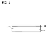
- a dielectric layer 15 (e.g., a silicon oxide and/or silicon nitride layer) is deposited on a polished front surface of a donor wafer 12.
- the dielectric layer 15 may be applied according to any known technique in the art, such as thermal oxidation, wet oxidation, chemical vapor deposition, thermal nitridation or a combination of these techniques.
- the dielectric layer 15 is grown to a substantially uniform thickness sufficient to provide the desired insulating properties in the final structure.
- the dielectric layer has a thickness of at least about 1 nm and less than about 10,000 nm, less than about 5,000 nm, less than about 1,000 nm, less than about 500 nm, less than about 150 nm, less than about 100 nm or even less than about 50 nm.
- the dielectric layer 15 may be any electrically insulating material suitable for use in a SOI structure, such as a material comprising SiO 2 Si 3 N 4 , aluminum oxide, or magnesium oxide.
- the dielectric layer 15 is SiO 2 (i.e., the dielectric layer consists essentially of SiO 2 with impurities being present therein).
- a material for the dielectric layer which has a melting point which is higher than the melting point of pure SiO 2 (i.e., higher than about 1700°C).
- materials are silicon nitride (Si 3 N 4 ), aluminum oxide, and magnesium oxide.
- Ions e.g., hydrogen atoms, helium atoms or a combination of hydrogen and helium atoms
- Ions are implanted at a substantially uniform specified depth beneath the front surface of the donor wafer to define a cleave plane 17. It should be noted, that when combinations of ions are implanted, they may be implanted concurrently or sequentially. Ion implantation may be achieved using means known in the art. For example, this implantation may be achieved in a manner similar to the process disclosed in U.S. Patent No. 6,790,747 .
- Implantation parameters may include, for example, implantation of ions to a total dose of about 1 x 10 15 to about 5 x 10 16 ions/cm 2 at a total energy of, for example, about 20 to about 125 keV (e.g., H 2 + may be implanted at an energy of 20 keV and a dose of 2.4 x 10 16 ions/cm 2 ).
- the dose may be adjusted between the combination of ions accordingly (e.g., He + may be implanted at an energy of 36 keV and a dose of 1 x 10 16 ions/cm 2 followed by H 2 + implanted at an energy of 48 keV and a dose of 5 x 10 15 ions/cm 2 ).
- the subsequent growth or deposition of the dielectric layer on the donor wafer is suitably performed at a temperature low enough to prevent premature separation or cleaving along plane 17 in the donor layer (i.e., prior to the wafer bonding process step).
- the separation or cleaving temperature is a complex function of the implanted species, implanted dose and implanted material. However, typically, premature separation or cleaving may be avoided by maintaining a deposition or growth temperature below about 500°C.
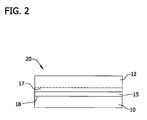
- the front surface of the dielectric layer 15 is then bonded to the front surface of a handle wafer 10 to form a bonded wafer 20 through a hydrophilic bonding process.
- the dielectric layer 15 and handle wafer 10 may be bonded together by exposing the surfaces of the wafers to a plasma containing, for example, oxygen or nitrogen. Exposure to the plasma modifies the structure of the surfaces in a process often referred to as surface activation. The wafers are then pressed together and a bond at the bond interface 18 is formed there between.
- the surfaces of the dielectric layer and handle wafer may optionally undergo cleaning and/or a brief etching, planarization, or plasma activation to prepare their surfaces for bonding using techniques known in the art. Without being held to a particular theory, it is generally believed that the quality of the silicon surface of the SOI structure is, in part, a function of the quality of the surface prior to bonding. Additionally, the quality of both surfaces prior to bonding will have a direct impact on the quality or strength of the resulting bond interface.
- the dielectric layer and/or handle wafer may be subjected to one or more of the following procedures in order to obtain, for example, a low surface roughness (e.g., a roughness of less than about 0.5 nm root mean square (RMS)) prior to bonding: (i) planarization by, for example, CMP and/or (ii) cleaning by, for example, a wet chemical cleaning procedure, such as a hydrophilic surface preparation process (e.g., an RCA SC-1 clean process wherein the surfaces are contacted with a solution containing ammonium hydroxide, hydrogen peroxide, and water at a ratio of, for example, 1:2:50 at about 65°C for about 20 minutes, followed by a deionized water rinse and drying).
- a hydrophilic surface preparation process e.g., an RCA SC-1 clean process wherein the surfaces are contacted with a solution containing ammonium hydroxide, hydrogen peroxide, and water at a ratio of, for example, 1:2:50 at about 65°
- One or both of the surfaces may also optionally be subjected to a plasma activation after, or instead of, the wet cleaning process to increase the resulting bond strength.
- the plasma environment may include, for example, oxygen, ammonia, argon, nitrogen, diborane or phosphine.
- wafer bonding may be achieved using essentially any technique known in the art, provided the energy employed to achieve formation of the bond interface is sufficient to ensure that the integrity of the bond interface is sustained during subsequent processing (i.e., layer transfer by separation along the cleave or separation plane 17 in the donor wafer).
- wafer bonding is achieved by contacting the surface of the dielectric layer and the handle wafer at a reduced pressure (e.g., about 50 mTorr) and at room temperature, followed by heating at an elevated temperature (e.g., at least about 200°C, at least about 300°C, at least about 400°C, or even at least about 500°C) for a sufficient period of time (e.g., at least about 10 seconds, at least about 1 minute, at least about 15 minutes, at least about 1 hour or even at least about 3 hours). For example, the heating may take place at about 350°C for about 1 hour.
- a reduced pressure e.g., about 50 mTorr
- an elevated temperature e.g., at least about 200°C, at least about 300°C, at least about 400°C, or even at least about 500°C
- a sufficient period of time e.g., at least about 10 seconds, at least about 1 minute, at least about 15 minutes, at least about 1 hour or even at least about 3 hours.
- the resulting interface may have a bond strength that is greater than about 500 mJ/m 2 , greater than about 1000 mJ/m 2 , greater than about 1500 mJ/m 2 , or even greater than about 2000 mJ/m 2 .
- the elevated temperatures cause the formation of covalent bonds between the adjoining surfaces of the donor wafer and the handle wafer, thus solidifying the bond between the donor wafer and the handle wafer.
- the ions earlier implanted in the donor wafer weaken the cleave plane.
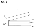
- a portion of the donor wafer is then separated (i.e., cleaved) along the cleave plane from the bonded wafer to form the SOI structure.
- the resulting bonded structure is subjected to conditions sufficient to induce a fracture along the separation or cleave plane within the donor wafer ( Fig. 3 ).
- this fracture may be achieved using techniques known in the art, such as thermally and/or mechanically induced cleaving techniques.
- fracturing is achieved by annealing the bonded structure at a temperature of at least about 200°C, at least about 300°C, at least about 400°C, at least about 500°C, at least about 600°C, at least about 700°C or even at least about 800°C (the temperature being in the range of, for example, about 200°C to about 800°C, or from about 250°C to about 650°C) for a period of at least about 10 seconds, at least about 1 minute, at least about 15 minutes, at least about 1 hour or even at least about 3 hours (with higher temperatures requiring shorter anneal times, and vice versa), under an inert (e.g., argon or nitrogen) atmosphere or ambient conditions.
- inert e.g., argon or nitrogen
- this separation may be induced or achieved by means of mechanical force, either alone or in addition to annealing.
- the bonded wafer may be placed in a fixture in which mechanical force is applied perpendicular to the opposing sides of the bonded wafer in order to pull a portion of the donor wafer apart from the bonded wafer.
- suction cups are utilized to apply the mechanical force.
- the separation of the portion of the donor wafer is initiated by applying a mechanical wedge at the edge of the bonded wafer at the cleave plane in order to initiate propagation of a crack along the cleave plane.
- the mechanical force applied by the suction cups then pulls the portion of the donor wafer from the bonded wafer, thus forming a SOI structure.
- Structure 30 comprises a portion of the donor wafer.
- Structure 31 is the silicon on insulator structure and includes the handle wafer 16, the dielectric layer 15, and a silicon layer 25.
- the resulting SOI structure 31 includes a thin layer of silicon 25 (the portion of the donor wafer remaining after cleaving) disposed atop the dielectric layer 15 and the handle wafer 10.
- the silicon device layer 25 is typically less than about 200 nm thick and the trend toward further miniaturization has led to development of structures with a device layer thickness of less than about 100 nm, less than about 75 nm, less than about 50 nm or even less than about 10 nm (e.g., from about 1 nm to about 200 nm, from about 50 nm to about 200 nm or from about 1 nm to about 10 nm).
- the cleave surface of the SOI structure (i.e., the thin layer of silicon of the donor wafer) has a rough surface that may be smoothed by additional processing.
- the structure 31 may be subjected to additional processing to produce a silicon layer surface having desirable features for device fabrication thereon. Such features include, for example, reduced surface roughness, and/or a reduced concentration of light point defects.
- annealing chemical-mechanical polishing, high-temperature gaseous etching (i.e., epitaxial-smoothing (epi-smoothing)), or the formation of a sacrificial oxide layer on the cleaved surface may be used.
- PESA Pre-epitaxial smoothing anneal
- an elevated temperature about 1000°C to about 1200°C
- the elevated temperature heals the cleaved surface of the SOI wafer by permitting the crystal structure of the silicon to reorient the dislocations present therein.
- any of the additionally processing operations e.g., PESA and/or epi-smoothing may be performed after the nickel reduction process described below.
- the various surfaces of the SOI structure 31 are often cleaned and/or polished during fabrication of the SOI structure to assist in bonding of the various surfaces.
- the top surface of the handle wafer 10 and the top surface of the dielectric layer 15 are both cleaned prior to bonding and the surface of the silicon layer 25 is polished and cleaned after cleavage.
- Each of these cleaning operations introduces metal contaminants into the wafer.
- the concentration of metal and, in particular, the concentration of nickel which is the principal metal contaminant in the structure may be at least about 1 x 10 10 atoms/cm 3 and in some applications may be at least about 1 x 10 11 atoms/cm 3 or at least about 1 x 10 12 atoms/cm 3 .
- the localized concentration in the silicon device layer 25 may be higher than the bulk concentration and device layer metal concentrations (and in particular the concentration of nickel) of at least about 1 x 10 10 atoms/cm 3 , at least about 1 x 10 12 atoms/cm 3 or at least about 1 x 10 14 atoms/cm 3 (e.g., from about 1 x 10 10 atoms/cm 3 to about 1 x 10 16 atoms/cm 3 ) are typical.
- Metal contaminants other than nickel may also be present such as, for example, copper and/or cobalt.
- the methods of the present disclosure are particularly well-suited for removing nickel which is more problematic when present in the silicon device layer 25 relative to other metals such as copper and cobalt.
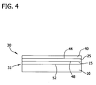
- a sacrificial oxide layer 40 is formed on the front surface of the silicon device layer 25.
- the sacrificial oxide layer 40 may be a native oxide layer that forms upon exposing the structure to ambient air. Such native oxide layers may be from about 5 ⁇ to about 15 ⁇ thick. (Throughout the description, 1 ⁇ equals 0.1nm.) For example, a native oxide layer may be about 10 ⁇ and typically about 8 ⁇ , (i.e., about 0.8 nm thick). Alternatively, the sacrificial oxide layer 40 may be formed by heating the wafer in an oxygen-containing atmosphere.
- a small amount of oxygen is added to the atmosphere in which the SOI structure is heated in step S 2 described below (i.e., steps S 1 and S 2 occur in the same apparatus (e.g., furnace) and may occur simultaneously).
- the thickness of the oxide layer is not critical and any thickness may be suitable.
- the sacrificial oxide layer need not be continuous on the surface of the silicon device layer, however it is preferred that any gaps in sacrificial oxide layer coverage be less than the device layer thickness.
- the sacrificial silicon oxide layer-containing structure has a first interface 44 formed between the sacrificial oxide layer 40 and the silicon device layer 25.
- a second interface 48 is formed between the device layer 25 and the dielectric layer 15 (e.g., the silicon oxide layer) and a third interface 52 is formed between the dielectric layer 15 and the handle wafer 10.
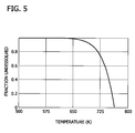
- T 1 should be chosen to be sufficiently high to allow essentially all nickel atoms in the device layer to dissolve (i.e., to dissociate from metal agglomerates within the device layer). T 1 should also not exceed a temperature at which the dissolved nickel atoms cross the sacrificial oxide layer-silicon device layer interface 44 and enter the sacrificial oxide layer 40. By maintaining T 1 below such temperatures, nickel atoms in the device layer 40 become "pinned" when they contact the sacrificial oxide layer-device layer interface 44 or contact the device layer-dielectric layer interface 48.
- T 1 is no more than about 25°C greater than the temperature at which the nickel completely dissolves in the device layer 25. In other embodiments T 1 is no more than about 20°C greater, no more than about 15°C greater, no more than about 10°C greater or even no more than about 5°C greater than the temperature at which the nickel completely dissolves in the device layer 25.
- T 1 is chosen such that essentially all of the nickel which is desired to be removed from the structure dissolves in the silicon layer.
- T 1 may be determined empirically. For example, a solubility function based on experimental data for nickel of which it is desired to reduce the concentration thereof may be used to determine T 1 .
- the solubility of nickel and silicon has been reported in INSPEC, EMIS Data Reviews, No. 4, Properties of Silicon, p.
- T 1 may be at least about 490°C, at least about 500°C or at least about 510°C.
- the wafer should be held at a temperature T 1 sufficient to dissolve essentially all of the nickel but less than a temperature at which the nickel atoms cross the oxide interfaces 44, 48 for a period of time t 1 sufficient to allow nickel atoms to substantially evenly disperse throughout the device layer. By allowing the nickel atoms to evenly disperse, the atoms are less likely to recombine during cooling and form nickel precipitates.
- the nickel atoms are "evenly dispersed" in the silicon layer when the mean axial diffusion distance of nickel atoms (i.e., the average distance at which nickel atoms travel toward either the sacrificial oxide layer-silicon device layer interface 44 or the device layer-dielectric layer interface 48) is many times larger the device layer thickness (e.g., at least about 100 times).
- the mean axial diffusion distance of nickel atoms is at least about 500 times the silicon device layer thickness or at least about 1000 times, at least about 2500 times or even at least about 5000 times the device layer thickness (e.g., from about 500 to about 10,000 times or from about 2500 to about 10,000 times the device layer thickness).
- the dispersal of nickel atoms in the device layer may also be observed by using destructive testing that involves various thermal cycles, precipitation and etching to delineate precipitates.
- D ⁇ Ni Si 2 ⁇ 10 - 3 ⁇ exp - / k B ⁇ T 0.47 ⁇ eV
- D(Ni) Si is expressed in cm 2 /sec
- T is in Kelvin
- K B is Boltzmann's constant (8.617 x 10 -5 eV/K).
- anneals of at least about 15 minutes may be used or even anneals as short as about 10 minutes or more, about 5 minutes or more or even as short as 1 minute or more may be used.
- T 1 need not be a single temperature at which the SOI structure is maintained for a period of time t 1 . Rather, the wafer may be maintained within a range of temperatures which allows essentially all of the nickel to be dissolved but is less than a temperature at which the nickel atoms cross the oxide interfaces 44, 48 for a time period t 1 sufficient to allow nickel atoms to substantially evenly disperse throughout the device layer.
- the wafer is cooled from T 1 to a temperature T 2 in step S 3 , T 2 being a temperature at which the nickel atoms are substantially immobile in silicon, at an average cooling rate of R.
- the cooling rate R is sufficiently low to cause substantially no nickel precipitation to occur in the silicon device layer during cooling.
- the nickel atoms in the device layer seek their lowest chemical potential which has been found to occur at the oxide interfaces 44, 48. If the wafer cools too slow, the nickel atoms may instead nucleate and combine into precipitates. Accordingly, the cooling rate R is controlled to be sufficiently fast to cause substantially no nickel precipitation to occur in the silicon device layer during cooling.
- the cooling rate of the silicon wafer may be maintained to be at least about 0.3°C/min or, as in other embodiments, at least about 1°C/sec, at least about 5°C/min, at least about 30°C/min, at least about 60°C/min or at least about 100°C/min (e.g., from about 0.3°C/min to about 5000 °C/min, from about 0.3°C/min to about 1000°C/min or from about 1°C/min to about 500°C/min).
- the temperature at which nickel atoms are substantially immobile in silicon is the temperature at which 80% of the nickel remains undissolved in silicon.
- nickel is substantially immobile in silicon at about 715°K (about 440°C) (i.e., T 2 is about 440°C or less). In other embodiments, T 2 is about 425°C or less, about 400°C or less or about 300°C or less.
- steps S 2 and S 3 may be performed in the same ambient and suitable ambients include gases which are inert with respect to silicon and silicon oxide atoms.
- the ambient comprises an amount of oxygen to grow a sacrificial oxide layer on the surface of the SOI structure in step S 1 as described above.
- the cooling rate has also to be high enough to cause a temperature gradient across the wafer such that the temperature at the sacrificial oxide layer-silicon device layer interface 44 exceeds the temperature at the silicon device layer-dielectric layer interface 48 during cooling.
- This gradient allows more nickel atoms to migrate and be pinned at the sacrificial oxide layer-silicon device layer interface 44 relative to the silicon device layer-dielectric layer interface 48 as nickel atoms at the silicon device layer-dielectric layer interface 48 are mobile for an increased amount of time compared to the nickel atoms at the sacrificial oxide layer-silicon device layer interface 44.
- Suitable cooling rates include rates of at least about 0.3°C/sec or even at least about 5°C/sec as described above.
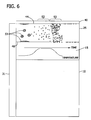
- FIG. 6 schematically shows a SOI wafer 31 with a sacrificial oxide layer 40 on the surface thereof.
- the temperature profile of the wafer as a function of time is shown within the dielectric layer 15.
- the device layer 25 includes a number of nickel precipitates 53.
- the precipitates dissolve and nickel atoms become evenly dispersed throughout the silicon device layer 25.
- the nickel atoms migrate to their lowest chemical potential which is at the oxide interfaces 44, 48, preferably with the greater amount migrating to the interface 44 with the native oxide layer 40 than the interface 48 with the dielectric layer 15.
- steps S 1 , S 2 and S 3 result in a SOI structure with a sacrificial oxide layer and a device layer comprising nickel atoms, wherein at least about 50% of the nickel atoms are positioned in the device layer at the interface 44 formed between the sacrificial oxide layer 40 and device layer 25. In some embodiments, at least about 55%, at least about 60% or even at least about 70% of the nickel atoms are positioned in the device layer at the interface 44.
- nickel atoms located "at the interface 44" either (i) make contact with both the device layer 25 and sacrificial oxide layer 40 or (ii) are within the device layer 25 at a distance from the interface 44, the distance being sufficiently small such that the atoms are accessible to conventional cleaning processes (i.e., are capable of being removed by such processes) after the sacrificial oxide layer is removed.
- the sacrificial oxide layer 40 is removed as well as the nickel atoms at the interface 44 therewith in step S 4 of the nickel-reducing process.
- the sacrificial oxide layer 40 and nickel atoms may be removed by contacting the SOI structure with an etching solution. Any suitable etching solution known to those of skill in the art for semiconductor cleaning may be used including SC1 (a NH 4 OH and H 2 O 2 mixture) and HF cleaning baths. Generally the solutions are applied under conditions suitable to remove the sacrificial oxide layer as may be determined by those of skill in the art.
- the surface of the SOI structure may be contacted with the etchant by immersing (or at least partially immersing) the SOI structure in an etchant bath or by selectively etching the surface by contacting the surface with an etchant gas (e.g., HF etchant gas).
- an etchant gas e.g., HF etchant gas
- Batch-immersion (cleaning benches) may be used for etching and spin etching techniques may also be used without departing from the scope of the present disclosure.
- the solution is an aqueous HF solution that may optionally contain an amount of H 2 O 2 .
- concentration of HF in the solution may be less than about 50% and, in other embodiments, is less than about 25%, less than about 10%, less than about 5% or less than about 2% (e.g., from about 0.5% to about 50% or from about 0.5% to about 10%).
- the HF solution may contain one or more other components such as complexing ligands or surfactants; however, in certain embodiments the etchant consists essentially of water and HF.
- the etchant may also be a gas that is contacted with the surface of the structure. Suitable gases include HF gas that may be diluted in a carrier gas such as hydrogen, argon or nitrogen.
- the period of time for which the etchant contacts the silicon layer may vary according to the corrosiveness of the etchant, its concentration and the thickness of the oxide that must be removed before the nickel atoms trapped at the device layer-sacrificial oxide interface are exposed and removed. For oxide thicknesses less than about 1 nm, time scales typical for conventionally-used SC1 or HF baths (no more than 18 minutes, and typically less than 5 minutes) may be used. In general, SC1 processing is followed by rinsing and acid treatment (i.e., a SC2 clean) to remove nickel deposited on the surface by the SC1 clean, as is conventional in the field of the present disclosure. Processing conditions are well known to those of skill in the art and any number of combinations of chemical baths and process times to remove the surface oxide and the nickel atoms pinned immediately underneath may be used without departing from the scope of the present disclosure.
- Step S 4 of the present disclosure results in removal of nickel atoms at the interface 44 which reduces the total nickel content of the silicon device layer.
- the total nickel content of the device layer may be reduced to the solubility limit of nickel in silicon at temperature T 1 or even below this solubility limit.
- steps S 1 , S 2 , S 3 and S 4 may be repeated for one or more additional cycles such as, for example, about 2 cycles or more, about 3 cycles or more or even about 5 cycles or more.
- EXAMPLE 1 Reduction of Nickel-Related Defects in SOI Wafers that were Pre-epitaxial Layer Smooth Annealed ( PESA ) but not Smoothed by Gas Etching (Epi-Smoothed)
- the decorative etch included a standard Secco etch to etch through to any metal precipitates followed by an HF etch to undercut the buried oxide layer in any areas where the Secco etch created a pathway to the BOX layer.
- the resulting pits were detected by a Kodak bright light. The defects were measured for each wafer in two different quadrants (tests "a” and "b” below).
- Results of the bright light assessment are shown in the "Defects Present?" column.
- the column titled “Extension” indicates the distance the wand haze extended from the edge of the wafer toward the center.
- a field of view of the wafer in an area were wand haze was present was selected to count defects.
- a random field of view was selected for wafers where no defects were observed. The microscope objective was chosen such that the defects could properly be counted. Only one field of view was used per quadrant.
- the total number of defects measured for each field of view is shown in the "Defect Count” column and the number of defects per cm 2 is shown in the "Defect Density” column.
- Table 1 Defect amounts in SOI wafers heated to 500°C for 15 minutes and in control wafers processed according to Example 1. Wafer Metal Reduction Treatment Etch Defects Present? Extension (mm) Objective Defect Count Defect Density (defects/ cm 2 ) 1a 500°C, 15 min HF None #N/A 1-5x 0 0 1b 500°C, 15 min HF None #N/A 1-5x 0 0 2a 500°C, 15 min HF+H 2 O 2 None #N/A 1-5x 0 0 2b 500°C, 15 min HF+H 2 O 2 None #N/A 1-5x 0 0 3a 500°C, 15 min HF None #N/A 1-5x 0 0 3b 500°C, 15 min HF None #N/A 1-5x 0 0 4a 500°C, 15 min HF+H 2 O 2 None #N/A 1-5x 0 0 4b 500°C, 15 min HF+H 2 O 2 None #N/
- a second wafer from each lot was also used as a control (4 control wafers).
- the heat-treated wafers were combined with the control wafers and all wafers received a HF clean, a final clean (SC1 and SC2 clean) and a final inspection on a particle inspection tool (SP207, KLA-Tencor (Milpitas, California)). All eight wafers were then subjected to Secco testing in accordance with the process set forth in Example 1 with the results being shown in Table 2.
- the wafer tested in lot 3 had two "hot spots" near the wafer edge.
- Table 2 Defect amounts in SOI wafers heated to 500°C for 15 minutes and in control wafers processed according to Example 2.
Description
- The field of the present disclosure relates to methods for producing silicon on insulator structures and, in particular, methods for producing silicon on insulator structures with a reduced nickel content in the device layer thereof.
- Silicon on insulator structures ("SOI structures" which may also be referred to herein as "SOI wafers" or "SOI substrates") generally include a handle wafer, a silicon layer (also characterized as a "device layer"), and a dielectric layer (such as an oxide layer) between the handle wafer and the silicon layer. Transistors built within the top silicon layer of SOI structures switch signals quickly compared to transistors built on bulk silicon wafers, run at lower voltages and are much less vulnerable to signal noise from background cosmic ray particles. Each transistor is isolated from its neighbor by a complete layer of silicon dioxide. These transistors are generally immune to "latch-up" problems and can be spaced closer together than transistors built on bulk silicon wafers. Building circuits on SOI structures increases productivity by allowing for more compact circuit designs, yielding more chips per wafer.
- Metal contamination in semiconductor wafers is detrimental as the contamination can cause yield losses in the resulting integrated circuits. Metal contamination has increasingly become a concern in view of the trend toward smaller devices, devices with faster operational speeds and lower manufacturing costs. Metal contamination may be introduced into semiconductor wafers in a number of processing steps including wafer polishing, cleaning, bond strength enhancing thermal treatment, epitaxy, oxide stripping, plasma activation, wet chemical etching, gas phase chemical etching, high temperature annealing, ion implantation, oxidation and the like. SOI wafers made by layer transfer are sensitive to metal contamination as the device layer is thin and three surfaces must be cleaned. Surface contamination can diffuse into the thin device layer at a higher concentration relatively to thicker bulk wafers.
- Furuhita et al., Japanese Journal Appl. Phys. 39(4B):2251-2255 describe the behavior of isotopes of metals like Fe, Ni, Cu in the silicon layer of ultrathin bonded SOI wafers.
US 6,077,731 A describes a semiconductor element made by introducing metal and thus preparing a crystalline silicon film, and subsequently eliminating the metal. - A continuing need exists for semiconductor wafers with a reduced nickel content and, in particular, silicon on insulator structures with a reduced nickel content in the device layer thereof. A continuing need also exists for methods for producing such wafers.
- The present disclosure is directed to a method for reducing the nickel content of a silicon on insulator structure. The silicon on insulator structure includes a handle wafer, a silicon device layer having a front surface and a dielectric layer between the handle wafer and the silicon device layer. The dielectric layer and silicon device layer form an interface between the dielectric layer and silicon device layer. A sacrificial oxide layer is formed on the front surface of the silicon device layer. The sacrificial oxide layer and the silicon device layer form an interface between the sacrificial oxide layer and the silicon device layer. The silicon on insulator structure having a sacrificial oxide layer thereon is heated to a temperature T1 sufficient to dissolve all nickel precipitates present in the device layer for a time t1 sufficient to allow nickel atoms to evenly disperse throughout the device layer. The temperature T1 is less than a temperature at which the nickel atoms cross the sacrificial oxide layer-silicon device layer interface and enter the sacrificial oxide layer. The silicon on insulator structure is cooled from T1 to a temperature T2 at which the nickel atoms are substantially immobile in silicon at an average cooling rate of R to cause nickel atoms to dissolve to the sacrificial oxide layer-silicon device layer interface and the silicon device layer-dielectric layer interface. The cooling rate is sufficiently high enough to cause substantially no nickel precipitation to occur in the silicon device layer during cooling. The sacrificial oxide layer and a portion of the nickel atoms at the sacrificial oxide layer-silicon device layer interface are removed from the silicon-in-insulator structure. The temperature at the sacrificial oxide layer-silicon device layer interface exceeds the temperature at the silicon device layer-dielectric layer interface during cooling such that more nickel atoms are positioned at the sacrificial oxide layer-silicon device layer interface than the silicon device layer-dielectric layer interface.
- Various refinements exist of the features noted in relation to the above-mentioned present disclosure. Further features may also be incorporated in the above-mentioned present disclosure as well. These refinements and additional features may exist individually or in any combination. For instance, various features discussed below in relation to any of the illustrated embodiments of the present disclosure may be incorporated into the above-described present disclosure, alone or in any combination.
-
-
Figure 1 is cross-section view of a donor wafer with a dielectric layer disposed thereon; -
Figure 2 is a cross-section view of the donor wafer and dielectric layer bonded to a handle wafer; -
Figure 3 is a cross-section view of the SOI structure upon cleaving the donor wafer at the cleave plane; -
Figure 4 is a SOI structure with a sacrificial oxide layer disposed thereon; -
Figure 5 is a graph depicting the solubility of nickel in silicon as a function of temperature; -
Figure 6 is a schematic view of a SOI structure which shows migration of nickel atoms in the silicon device layer; and -
Figure 7 is a graph showing the temperature profile of the wafer during processing according to Example 1. - Corresponding reference characters indicate corresponding parts throughout the drawings.
- In accordance with the present disclosure, the nickel content in the device layer of a silicon on insulator structure may be reduced by forming a sacrificial oxide layer on the surface of the silicon on insulator structure in a first step S1. As schematically shown in
Figure 6 , the structure is heated to a temperature at which a particular nickel contaminant (e.g., nickel precipitates) dissolves for a sufficient amount of time to allow the nickel atoms to evenly disperse throughout the device layer in step S2. The cooling rate of the SOI structure is controlled in step S3 to allow the nickel atoms to migrate to and become "pinned" at the interface between the sacrificial oxide layer and the device layer. The sacrificial oxide layer and nickel atoms at the interface therewith are removed by etching in step S4 to reduce the concentration of contaminants in the device layer. The process may be repeated in one or more additional cycles to further reduce the concentration of nickel in the device layer. - Multi-layered structures and, in particular, silicon on insulator structures and methods for producing silicon on insulator structures are generally known by those skilled in the art (see, for example,
U.S. Pat. Nos. 5,189,500 ;5,436,175 and6,790,747 ). In an exemplary process for making a multi-layered structure, two separate structures are prepared, bonded together along a bond interface, and then delaminated (i.e., cleaved) along a separation plane that is different from the bond interface and which has been formed via an implantation technique. One structure is typically referred to as the "handle" wafer (or structure) and the other is typically referred to as the "donor" wafer (or structure). - A dielectric layer may be deposited on the surface of the donor wafer, the handle wafer or both, prior to bonding the donor and handle together. In this regard, the SOI structures and methods for preparing the SOI structures are described herein as having a dielectric layer deposited or grown on the donor wafer and as having the surface of the handle wafer bonded to the surface of the dielectric layer. However, it should be understood that the dielectric layer may be grown or deposited on the handle wafer alternatively or in addition to growing or depositing the dielectric layer on the donor wafer and that these structures may be bonded in any of the various arrangements without limitation. Reference herein to the dielectric layer being disposed on the handle wafer alone should not be considered in a limiting sense.
- Typically, at least the donor wafer and more typically both the donor wafer and the handle wafer are composed of single crystal silicon wafers, however it should be noted that other starting structures may be used such as multi-layered and/or heterolayered structures without departing from the present disclosure.
- The handle wafer may be obtained from any material common in the art for preparing multi-layered structures, such as silicon, germanium, gallium arsenide, silicon germanium, gallium nitride, aluminum nitride, phosphorous, quartz, sapphire and combinations thereof. Similarly, the donor wafer may contain silicon, germanium, gallium arsenide, silicon germanium, gallium nitride, aluminum nitride, phosphorous, quartz, sapphire and combinations thereof. Typically however, the handle wafers and donor wafers used according to the methods of the present disclosure are single crystal silicon wafers and generally are single crystal silicon wafers which have been sliced from a single crystal ingot grown in accordance with conventional Czochralski crystal growing methods. As such, the following discussion frequently refers to a specific type of multi-layered structure, i.e., SOI structures, for illustrative purposes. In this regard, it should be noted that the handle wafer and/or the donor wafer used in accordance with the present disclosure may be any diameter suitable for use by those of skill in the art including, for example, 200 mm, 300 mm, greater than 300 mm or even 450 mm diameter wafers.
- Referring to
Figure 1 , a dielectric layer 15 (e.g., a silicon oxide and/or silicon nitride layer) is deposited on a polished front surface of adonor wafer 12. Thedielectric layer 15 may be applied according to any known technique in the art, such as thermal oxidation, wet oxidation, chemical vapor deposition, thermal nitridation or a combination of these techniques. Generally speaking, thedielectric layer 15 is grown to a substantially uniform thickness sufficient to provide the desired insulating properties in the final structure. Typically, however, the dielectric layer has a thickness of at least about 1 nm and less than about 10,000 nm, less than about 5,000 nm, less than about 1,000 nm, less than about 500 nm, less than about 150 nm, less than about 100 nm or even less than about 50 nm. Thedielectric layer 15 may be any electrically insulating material suitable for use in a SOI structure, such as a material comprising SiO2 Si3N4, aluminum oxide, or magnesium oxide. In some embodiments, thedielectric layer 15 is SiO2 (i.e., the dielectric layer consists essentially of SiO2 with impurities being present therein). However, it is to be noted that in some instances, it may alternatively be preferable to use a material for the dielectric layer which has a melting point which is higher than the melting point of pure SiO2 (i.e., higher than about 1700°C). Examples of such materials are silicon nitride (Si3N4), aluminum oxide, and magnesium oxide. - Ions (e.g., hydrogen atoms, helium atoms or a combination of hydrogen and helium atoms) are implanted at a substantially uniform specified depth beneath the front surface of the donor wafer to define a
cleave plane 17. It should be noted, that when combinations of ions are implanted, they may be implanted concurrently or sequentially. Ion implantation may be achieved using means known in the art. For example, this implantation may be achieved in a manner similar to the process disclosed inU.S. Patent No. 6,790,747 . Implantation parameters may include, for example, implantation of ions to a total dose of about 1 x 10¹⁵ to about 5 x 10¹⁶ ions/cm2 at a total energy of, for example, about 20 to about 125 keV (e.g., H2 + may be implanted at an energy of 20 keV and a dose of 2.4 x 10¹⁶ ions/cm2). When a combination of ions is used, the dose may be adjusted between the combination of ions accordingly (e.g., He+ may be implanted at an energy of 36 keV and a dose of 1 x 10¹⁶ ions/cm2 followed by H2 + implanted at an energy of 48 keV and a dose of 5 x 10¹⁵ ions/cm2). - When implantation is performed prior to deposition of the dielectric layer, the subsequent growth or deposition of the dielectric layer on the donor wafer is suitably performed at a temperature low enough to prevent premature separation or cleaving along
plane 17 in the donor layer (i.e., prior to the wafer bonding process step). The separation or cleaving temperature is a complex function of the implanted species, implanted dose and implanted material. However, typically, premature separation or cleaving may be avoided by maintaining a deposition or growth temperature below about 500°C. - Referring now to
Figure 2 , the front surface of thedielectric layer 15 is then bonded to the front surface of ahandle wafer 10 to form a bondedwafer 20 through a hydrophilic bonding process. Thedielectric layer 15 and handlewafer 10 may be bonded together by exposing the surfaces of the wafers to a plasma containing, for example, oxygen or nitrogen. Exposure to the plasma modifies the structure of the surfaces in a process often referred to as surface activation. The wafers are then pressed together and a bond at thebond interface 18 is formed there between. - Prior to bonding, the surfaces of the dielectric layer and handle wafer may optionally undergo cleaning and/or a brief etching, planarization, or plasma activation to prepare their surfaces for bonding using techniques known in the art. Without being held to a particular theory, it is generally believed that the quality of the silicon surface of the SOI structure is, in part, a function of the quality of the surface prior to bonding. Additionally, the quality of both surfaces prior to bonding will have a direct impact on the quality or strength of the resulting bond interface.
- In some instances, therefore, the dielectric layer and/or handle wafer may be subjected to one or more of the following procedures in order to obtain, for example, a low surface roughness (e.g., a roughness of less than about 0.5 nm root mean square (RMS)) prior to bonding: (i) planarization by, for example, CMP and/or (ii) cleaning by, for example, a wet chemical cleaning procedure, such as a hydrophilic surface preparation process (e.g., an RCA SC-1 clean process wherein the surfaces are contacted with a solution containing ammonium hydroxide, hydrogen peroxide, and water at a ratio of, for example, 1:2:50 at about 65°C for about 20 minutes, followed by a deionized water rinse and drying). One or both of the surfaces may also optionally be subjected to a plasma activation after, or instead of, the wet cleaning process to increase the resulting bond strength. The plasma environment may include, for example, oxygen, ammonia, argon, nitrogen, diborane or phosphine.
- Generally speaking, wafer bonding may be achieved using essentially any technique known in the art, provided the energy employed to achieve formation of the bond interface is sufficient to ensure that the integrity of the bond interface is sustained during subsequent processing (i.e., layer transfer by separation along the cleave or
separation plane 17 in the donor wafer). Typically, however, wafer bonding is achieved by contacting the surface of the dielectric layer and the handle wafer at a reduced pressure (e.g., about 50 mTorr) and at room temperature, followed by heating at an elevated temperature (e.g., at least about 200°C, at least about 300°C, at least about 400°C, or even at least about 500°C) for a sufficient period of time (e.g., at least about 10 seconds, at least about 1 minute, at least about 15 minutes, at least about 1 hour or even at least about 3 hours). For example, the heating may take place at about 350°C for about 1 hour. The resulting interface may have a bond strength that is greater than about 500 mJ/m2, greater than about 1000 mJ/m2, greater than about 1500 mJ/m2, or even greater than about 2000 mJ/m2. The elevated temperatures cause the formation of covalent bonds between the adjoining surfaces of the donor wafer and the handle wafer, thus solidifying the bond between the donor wafer and the handle wafer. Concurrently with the heating or annealing of the bonded wafer, the ions earlier implanted in the donor wafer weaken the cleave plane. A portion of the donor wafer is then separated (i.e., cleaved) along the cleave plane from the bonded wafer to form the SOI structure. - After the bond interface has been formed, the resulting bonded structure is subjected to conditions sufficient to induce a fracture along the separation or cleave plane within the donor wafer (
Fig. 3 ). Generally speaking, this fracture may be achieved using techniques known in the art, such as thermally and/or mechanically induced cleaving techniques. Typically, however, fracturing is achieved by annealing the bonded structure at a temperature of at least about 200°C, at least about 300°C, at least about 400°C, at least about 500°C, at least about 600°C, at least about 700°C or even at least about 800°C (the temperature being in the range of, for example, about 200°C to about 800°C, or from about 250°C to about 650°C) for a period of at least about 10 seconds, at least about 1 minute, at least about 15 minutes, at least about 1 hour or even at least about 3 hours (with higher temperatures requiring shorter anneal times, and vice versa), under an inert (e.g., argon or nitrogen) atmosphere or ambient conditions. - In this regard it is to be noted that in an alternative embodiment, this separation may be induced or achieved by means of mechanical force, either alone or in addition to annealing. For instance, the bonded wafer may be placed in a fixture in which mechanical force is applied perpendicular to the opposing sides of the bonded wafer in order to pull a portion of the donor wafer apart from the bonded wafer. According to some methods, suction cups are utilized to apply the mechanical force. The separation of the portion of the donor wafer is initiated by applying a mechanical wedge at the edge of the bonded wafer at the cleave plane in order to initiate propagation of a crack along the cleave plane. The mechanical force applied by the suction cups then pulls the portion of the donor wafer from the bonded wafer, thus forming a SOI structure.
- Referring to
Figure 3 , upon separation, twostructures structure 20 occurs along thecleave plane 17 in the donor wafer 12 (Fig. 2 ), a portion of the donor wafer remains part of both structures (i.e., a portion of the donor wafer is transferred along with the dielectric layer).Structure 30 comprises a portion of the donor wafer.Structure 31 is the silicon on insulator structure and includes the handle wafer 16, thedielectric layer 15, and asilicon layer 25. - The resulting
SOI structure 31 includes a thin layer of silicon 25 (the portion of the donor wafer remaining after cleaving) disposed atop thedielectric layer 15 and thehandle wafer 10. Thesilicon device layer 25 is typically less than about 200 nm thick and the trend toward further miniaturization has led to development of structures with a device layer thickness of less than about 100 nm, less than about 75 nm, less than about 50 nm or even less than about 10 nm (e.g., from about 1 nm to about 200 nm, from about 50 nm to about 200 nm or from about 1 nm to about 10 nm). - The cleave surface of the SOI structure (i.e., the thin layer of silicon of the donor wafer) has a rough surface that may be smoothed by additional processing. The
structure 31 may be subjected to additional processing to produce a silicon layer surface having desirable features for device fabrication thereon. Such features include, for example, reduced surface roughness, and/or a reduced concentration of light point defects. To smooth and thin the surface layer of silicon (i.e., cleaved surface), combinations of annealing, chemical-mechanical polishing, high-temperature gaseous etching (i.e., epitaxial-smoothing (epi-smoothing)), or the formation of a sacrificial oxide layer on the cleaved surface may be used. Pre-epitaxial smoothing anneal (PESA) processes that subject the SOI wafer to an elevated temperature (about 1000°C to about 1200°C) for several hours may be used. The elevated temperature heals the cleaved surface of the SOI wafer by permitting the crystal structure of the silicon to reorient the dislocations present therein. Alternatively, any of the additionally processing operations (e.g., PESA and/or epi-smoothing) may be performed after the nickel reduction process described below. - As described above, the various surfaces of the
SOI structure 31 are often cleaned and/or polished during fabrication of the SOI structure to assist in bonding of the various surfaces. For instance, the top surface of thehandle wafer 10 and the top surface of thedielectric layer 15 are both cleaned prior to bonding and the surface of thesilicon layer 25 is polished and cleaned after cleavage. Each of these cleaning operations introduces metal contaminants into the wafer. The concentration of metal and, in particular, the concentration of nickel which is the principal metal contaminant in the structure (i.e., the concentration in the structure as a whole or "bulk" concentration), may be at least about 1 x 10¹⁰ atoms/cm3 and in some applications may be at least about 1 x 10¹¹ atoms/cm3 or at least about 1 x 10¹² atoms/cm3. The localized concentration in thesilicon device layer 25 may be higher than the bulk concentration and device layer metal concentrations (and in particular the concentration of nickel) of at least about 1 x 10¹⁰ atoms/cm3, at least about 1 x 10¹² atoms/cm3 or at least about 1 x 10¹⁴ atoms/cm3 (e.g., from about 1 x 10¹⁰ atoms/cm3 to about 1 x 10¹⁶ atoms/cm3) are typical. Metal contaminants other than nickel may also be present such as, for example, copper and/or cobalt. In this regard, the methods of the present disclosure are particularly well-suited for removing nickel which is more problematic when present in thesilicon device layer 25 relative to other metals such as copper and cobalt. - In a first step S1 of the nickel-reducing process and as shown in
Figure 4 , asacrificial oxide layer 40 is formed on the front surface of thesilicon device layer 25. Thesacrificial oxide layer 40 may be a native oxide layer that forms upon exposing the structure to ambient air. Such native oxide layers may be from about 5 Å to about 15 Å thick. (Throughout the description, 1 Å equals 0.1nm.) For example, a native oxide layer may be about 10 Å and typically about 8 Å, (i.e., about 0.8 nm thick). Alternatively, thesacrificial oxide layer 40 may be formed by heating the wafer in an oxygen-containing atmosphere. In several embodiments, a small amount of oxygen is added to the atmosphere in which the SOI structure is heated in step S2 described below (i.e., steps S1 and S2 occur in the same apparatus (e.g., furnace) and may occur simultaneously). The thickness of the oxide layer is not critical and any thickness may be suitable. In this regard, the sacrificial oxide layer need not be continuous on the surface of the silicon device layer, however it is preferred that any gaps in sacrificial oxide layer coverage be less than the device layer thickness. - The methods of the present disclosure for reducing the nickel content of the SOI structure may be described in relation to several interfaces within the structure. As shown in
Figure 4 , the sacrificial silicon oxide layer-containing structure has afirst interface 44 formed between thesacrificial oxide layer 40 and thesilicon device layer 25. Asecond interface 48 is formed between thedevice layer 25 and the dielectric layer 15 (e.g., the silicon oxide layer) and athird interface 52 is formed between thedielectric layer 15 and thehandle wafer 10. - After the
sacrificial oxide layer 40 is formed, in step S2 of the nickel-reducing process, the silicon on insulator structure is heated to a temperature T1. T1 should be chosen to be sufficiently high to allow essentially all nickel atoms in the device layer to dissolve (i.e., to dissociate from metal agglomerates within the device layer). T1 should also not exceed a temperature at which the dissolved nickel atoms cross the sacrificial oxide layer-silicondevice layer interface 44 and enter thesacrificial oxide layer 40. By maintaining T1 below such temperatures, nickel atoms in thedevice layer 40 become "pinned" when they contact the sacrificial oxide layer-device layer interface 44 or contact the device layer-dielectric layer interface 48. It has been found that at temperatures above the dissolution temperature of nickel in the device layer, dissolved nickel atoms have a chemical potential at the various device layer-oxide interfaces that is lower than the chemical potential for atoms within the bulk which causes the nickel atoms to become "pinned" or "trapped" at the respective interface. However, if the temperature T1 of the structures exceeds a critical value, nickel atoms may cross the various oxide interfaces. This may be problematic as nickel from the bulk of the SOI wafer may then cross the dielectric layer and enter the silicon device layer. Additionally, nickel that has diffused into oxides may dissolve into the oxide but not migrate to the surface which may require hotter, longer processes with lower throughput. Further, temperatures at which nickel atoms cross the oxide surface may cause an engineered bulk microdefect density profile (e.g., oxygen precipitates or nuclei thereof) to become altered. Accordingly, it is preferred that T1 is no more than about 25°C greater than the temperature at which the nickel completely dissolves in thedevice layer 25. In other embodiments T1 is no more than about 20°C greater, no more than about 15°C greater, no more than about 10°C greater or even no more than about 5°C greater than the temperature at which the nickel completely dissolves in thedevice layer 25. - As stated above, T1 is chosen such that essentially all of the nickel which is desired to be removed from the structure dissolves in the silicon layer. T1 may be determined empirically. For example, a solubility function based on experimental data for nickel of which it is desired to reduce the concentration thereof may be used to determine T1. In the case of nickel in the silicon device layer, the solubility of nickel and silicon has been reported in INSPEC, EMIS Data Reviews, No. 4, Properties of Silicon, p. 446 (1988) (extrapolated to low temperatures) as

Figure 5 . As can be seen fromFigure 5 , nickel appears to be completely soluble at temperatures above about 760°K (above about 490°C). Accordingly, in embodiments of the present disclosure in which it is desired to remove nickel, T1 may be at least about 490°C, at least about 500°C or at least about 510°C. - The wafer should be held at a temperature T1 sufficient to dissolve essentially all of the nickel but less than a temperature at which the nickel atoms cross the oxide interfaces 44, 48 for a period of time t1 sufficient to allow nickel atoms to substantially evenly disperse throughout the device layer. By allowing the nickel atoms to evenly disperse, the atoms are less likely to recombine during cooling and form nickel precipitates. In this regard, for purposes of the present disclosure, the nickel atoms are "evenly dispersed" in the silicon layer when the mean axial diffusion distance of nickel atoms (i.e., the average distance at which nickel atoms travel toward either the sacrificial oxide layer-silicon
device layer interface 44 or the device layer-dielectric layer interface 48) is many times larger the device layer thickness (e.g., at least about 100 times). In some embodiments, the mean axial diffusion distance of nickel atoms is at least about 500 times the silicon device layer thickness or at least about 1000 times, at least about 2500 times or even at least about 5000 times the device layer thickness (e.g., from about 500 to about 10,000 times or from about 2500 to about 10,000 times the device layer thickness). The dispersal of nickel atoms in the device layer may also be observed by using destructive testing that involves various thermal cycles, precipitation and etching to delineate precipitates. - In this regard, the mean axial diffusion distance of nickel atoms may be determined from an experimentally determined diffusivity function and by the following equation which relates diffusivity and soak time to the mean axial diffusion distance, d.

For nickel in the silicon device layer, the diffusivity D has been reported in INSPEC, EMIS Data Reviews, No. 4, Properties of Silicon, p. 424 (1988) (extrapolated to low temperatures) as
where D(Ni)Si is expressed in cm2/sec, T is in Kelvin and KB is Boltzmann's constant (8.617 x 10⁻⁵ eV/K). Suitably for nickel atoms in the silicon device layer, at an anneal temperature ranging from 490°C to about 515°C, anneals of at least about 15 minutes (corresponding to a mean axial diffusion distance of about 0.79 mm at a temperature of about 500°C which is at least 4000 times the thickness of typical device layers) may be used or even anneals as short as about 10 minutes or more, about 5 minutes or more or even as short as 1 minute or more may be used. - Further in this regard, it should be understood that, for purposes of the present disclosure, T1 need not be a single temperature at which the SOI structure is maintained for a period of time t1. Rather, the wafer may be maintained within a range of temperatures which allows essentially all of the nickel to be dissolved but is less than a temperature at which the nickel atoms cross the oxide interfaces 44, 48 for a time period t1 sufficient to allow nickel atoms to substantially evenly disperse throughout the device layer.
- After time period t1, the wafer is cooled from T1 to a temperature T2 in step S3, T2 being a temperature at which the nickel atoms are substantially immobile in silicon, at an average cooling rate of R. The cooling rate R is sufficiently low to cause substantially no nickel precipitation to occur in the silicon device layer during cooling. As the wafer cools, the nickel atoms in the device layer seek their lowest chemical potential which has been found to occur at the oxide interfaces 44, 48. If the wafer cools too slow, the nickel atoms may instead nucleate and combine into precipitates. Accordingly, the cooling rate R is controlled to be sufficiently fast to cause substantially no nickel precipitation to occur in the silicon device layer during cooling. Suitably, the cooling rate of the silicon wafer may be maintained to be at least about 0.3°C/min or, as in other embodiments, at least about 1°C/sec, at least about 5°C/min, at least about 30°C/min, at least about 60°C/min or at least about 100°C/min (e.g., from about 0.3°C/min to about 5000 °C/min, from about 0.3°C/min to about 1000°C/min or from about 1°C/min to about 500°C/min).
- For purposes of the present disclosure, the temperature at which nickel atoms are substantially immobile in silicon is the temperature at which 80% of the nickel remains undissolved in silicon. As can be seen from
Figure 5 , nickel is substantially immobile in silicon at about 715°K (about 440°C) (i.e., T2 is about 440°C or less). In other embodiments, T2 is about 425°C or less, about 400°C or less or about 300°C or less. It should be noted that steps S2 and S3 may be performed in the same ambient and suitable ambients include gases which are inert with respect to silicon and silicon oxide atoms. In some embodiments, the ambient comprises an amount of oxygen to grow a sacrificial oxide layer on the surface of the SOI structure in step S1 as described above. - In addition to controlling the cooling rate such that substantially no nickel precipitation occurs in the silicon device layer during cooling, the cooling rate has also to be high enough to cause a temperature gradient across the wafer such that the temperature at the sacrificial oxide layer-silicon
device layer interface 44 exceeds the temperature at the silicon device layer-dielectric layer interface 48 during cooling. This gradient allows more nickel atoms to migrate and be pinned at the sacrificial oxide layer-silicondevice layer interface 44 relative to the silicon device layer-dielectric layer interface 48 as nickel atoms at the silicon device layer-dielectric layer interface 48 are mobile for an increased amount of time compared to the nickel atoms at the sacrificial oxide layer-silicondevice layer interface 44. Suitable cooling rates include rates of at least about 0.3°C/sec or even at least about 5°C/sec as described above. - The movement of nickel during steps S2 and S3 of the present disclosure is shown schematically in
Figure 6. Figure 6 schematically shows aSOI wafer 31 with asacrificial oxide layer 40 on the surface thereof. The temperature profile of the wafer as a function of time is shown within thedielectric layer 15. Before step S2, thedevice layer 25 includes a number of nickel precipitates 53. Upon heating during step S2, the precipitates dissolve and nickel atoms become evenly dispersed throughout thesilicon device layer 25. During cooling in step S3, the nickel atoms migrate to their lowest chemical potential which is at the oxide interfaces 44, 48, preferably with the greater amount migrating to theinterface 44 with thenative oxide layer 40 than theinterface 48 with thedielectric layer 15. In this regard, steps S1, S2 and S3 result in a SOI structure with a sacrificial oxide layer and a device layer comprising nickel atoms, wherein at least about 50% of the nickel atoms are positioned in the device layer at theinterface 44 formed between thesacrificial oxide layer 40 anddevice layer 25. In some embodiments, at least about 55%, at least about 60% or even at least about 70% of the nickel atoms are positioned in the device layer at theinterface 44. It should be noted that, as used herein, nickel atoms located "at theinterface 44" either (i) make contact with both thedevice layer 25 andsacrificial oxide layer 40 or (ii) are within thedevice layer 25 at a distance from theinterface 44, the distance being sufficiently small such that the atoms are accessible to conventional cleaning processes (i.e., are capable of being removed by such processes) after the sacrificial oxide layer is removed. - The
sacrificial oxide layer 40 is removed as well as the nickel atoms at theinterface 44 therewith in step S4 of the nickel-reducing process. Thesacrificial oxide layer 40 and nickel atoms may be removed by contacting the SOI structure with an etching solution. Any suitable etching solution known to those of skill in the art for semiconductor cleaning may be used including SC1 (a NH4OH and H2O2 mixture) and HF cleaning baths. Generally the solutions are applied under conditions suitable to remove the sacrificial oxide layer as may be determined by those of skill in the art. The surface of the SOI structure may be contacted with the etchant by immersing (or at least partially immersing) the SOI structure in an etchant bath or by selectively etching the surface by contacting the surface with an etchant gas (e.g., HF etchant gas). Batch-immersion (cleaning benches) may be used for etching and spin etching techniques may also be used without departing from the scope of the present disclosure. - In some particular embodiments, the solution is an aqueous HF solution that may optionally contain an amount of H2O2. The concentration of HF in the solution (by weight) may be less than about 50% and, in other embodiments, is less than about 25%, less than about 10%, less than about 5% or less than about 2% (e.g., from about 0.5% to about 50% or from about 0.5% to about 10%). The HF solution may contain one or more other components such as complexing ligands or surfactants; however, in certain embodiments the etchant consists essentially of water and HF. The etchant may also be a gas that is contacted with the surface of the structure. Suitable gases include HF gas that may be diluted in a carrier gas such as hydrogen, argon or nitrogen.
- The period of time for which the etchant contacts the silicon layer may vary according to the corrosiveness of the etchant, its concentration and the thickness of the oxide that must be removed before the nickel atoms trapped at the device layer-sacrificial oxide interface are exposed and removed. For oxide thicknesses less than about 1 nm, time scales typical for conventionally-used SC1 or HF baths (no more than 18 minutes, and typically less than 5 minutes) may be used. In general, SC1 processing is followed by rinsing and acid treatment (i.e., a SC2 clean) to remove nickel deposited on the surface by the SC1 clean, as is conventional in the field of the present disclosure. Processing conditions are well known to those of skill in the art and any number of combinations of chemical baths and process times to remove the surface oxide and the nickel atoms pinned immediately underneath may be used without departing from the scope of the present disclosure.
- Step S4 of the present disclosure results in removal of nickel atoms at the
interface 44 which reduces the total nickel content of the silicon device layer. For instance, the total nickel content of the device layer may be reduced to the solubility limit of nickel in silicon at temperature T1 or even below this solubility limit. - To further reduce the nickel content in the silicon device layer, steps S1, S2, S3 and S4 may be repeated for one or more additional cycles such as, for example, about 2 cycles or more, about 3 cycles or more or even about 5 cycles or more.
- Eight SOI wafers with Secco wand haze (i.e., very scattered visible light caused by small nickel precipitates) and which had a native oxide layer at the surface thereof were tested. The SOI wafers had been bonded, cleaved and annealed at 1125°C (i.e., pre-epitaxial layer smooth annealing (PESA)) but had not been subjected to high-temperature gaseous etching (i.e., epitaxial-smoothing (epi-smoothing)). Four wafers were used as a control and the four remaining wafers were heated to 500°C in a vertical furnace (A412, ASM (The Netherlands)) for 15 minutes with a small amount of oxygen insufficient to grow appreciable oxide (<3Å). The temperature profile for the wafers is illustrated in
Figure 7 in which the temperatures for the various paddle zones of the furnace are shown. The ramp down cooling rate was about 1.8°C/min. - Two wafers that were annealed at 500°C were then etched by use of a HF solution for 8 minutes and the other two were etched by use of a HF/H2O2 solution for 8 minutes. The concentration of HF was about 0.5 wt% and, when used, the concentration of H2O2 was about 2.5 wt%. All wafers were then epi-smoothed (E3000 EPI reactor, ASM (The Netherlands)) in a two step etching process in which the wafers were heated to 1100°C for a set period of time and then cooled to 1000°C while contacting the wafers with about a 0.7 vol% HCl in hydrogen ambient. Defects were measured by highlighting metal precipitates using a decorative etch. The decorative etch included a standard Secco etch to etch through to any metal precipitates followed by an HF etch to undercut the buried oxide layer in any areas where the Secco etch created a pathway to the BOX layer. The resulting pits were detected by a Kodak bright light. The defects were measured for each wafer in two different quadrants (tests "a" and "b" below).
- The results of the test are shown in Table 1 below. Results of the bright light assessment are shown in the "Defects Present?" column. The column titled "Extension" indicates the distance the wand haze extended from the edge of the wafer toward the center. A field of view of the wafer in an area were wand haze was present was selected to count defects. A random field of view was selected for wafers where no defects were observed. The microscope objective was chosen such that the defects could properly be counted. Only one field of view was used per quadrant. The total number of defects measured for each field of view is shown in the "Defect Count" column and the number of defects per cm2 is shown in the "Defect Density" column.
Table 1: Defect amounts in SOI wafers heated to 500°C for 15 minutes and in control wafers processed according to Example 1. Wafer Metal Reduction Treatment Etch Defects Present? Extension (mm) Objective Defect Count Defect Density (defects/ cm2) 1a 500°C, 15 min HF None #N/A 1-5x 0 0 1b 500°C, 15 min HF None #N/A 1-5x 0 0 2a 500°C, 15 min HF+H2O2 None #N/A 1-5x 0 0 2b 500°C, 15 min HF+H2O2 None #N/A 1-5x 0 0 3a 500°C, 15 min HF None #N/A 1-5x 0 0 3b 500°C, 15 min HF None #N/A 1-5x 0 0 4a 500°C, 15 min HF+H2O2 None #N/A 1-5x 0 0 4b 500°C, 15 min HF+H2O2 None #N/A 1-5x 0 0 5a None HF Wand Haze 30 2-20x 7 1892 5b None HF Wand Haze 42 2-20x 6 1622 6a None HF+H2O2 Wand Haze 36 2-20x 17 4595 6b None HF+H2O2 Wand Haze 33 2-20x 3 811 7a None HF+H2O2 Wand Haze 33 2-20x 6 1622 7b None HF+H2O2 Wand Haze 30 2-20x 6 1622 8a None HF Wand Haze 33 2-20x 4 1081 8b None HF Wand Haze 30 2-20x 2 541 - All defects are believed to be attributable to nickel due to its behavior and the thermal recipe used in the processing recipes. As can be seen from Table 1, the 500°C heat treatment resulted in no defects being detected.
- Four end-of-line SOI wafers (i.e., wafers that were processed as in Example 1 and then processed through a final cleaning and subjected to applicable inspections (particles, flatness and layer thickness inspections)) that had Secco wand haze were heated according to the process of Example 1 (500°C for 15 minutes with 1.8°C/min ramp down). As these wafers had previously been stripped of the native oxide layer, the sacrificial oxide layer was formed during annealing as a result of the partial pressure of oxygen present during heating. Each wafer was selected from a lot of wafers that were graded into one of four defect categories depending on the extent to which one wafer in the lot contained Secco wand haze. A second wafer from each lot was also used as a control (4 control wafers). After the 500°C heat treatment, the heat-treated wafers were combined with the control wafers and all wafers received a HF clean, a final clean (SC1 and SC2 clean) and a final inspection on a particle inspection tool (SP207, KLA-Tencor (Milpitas, California)). All eight wafers were then subjected to Secco testing in accordance with the process set forth in Example 1 with the results being shown in Table 2. The wafer tested in
lot 3 had two "hot spots" near the wafer edge.Table 2: Defect amounts in SOI wafers heated to 500°C for 15 minutes and in control wafers processed according to Example 2. Wafer Lot Metal Reduction Treatment Etch Defect Grading Quadrant Tested Defect Class Extension (mm) Objective Defect Count Density (defects/cm2) 1a None HF Edge Band 1 None N/A 1-5x 0 0 1b None HF Edge Band 4 None N/A 1-5x 0 0 2a None HF Light Wand Haze 1 Wand Haze 30 1-5x 147 2450 2b None HF Light Wand Haze 4 Wand Haze 30 1-5x 16 267 2c None HF Light Wand Haze 4 Hot Spot 4 1-5x 246 4100 3a None HF Heavy Wand Haze, small extension 1 Wand Haze 3 1-5x 189 3150 3b None HF Heavy Wand Haze, small extension 4 Wand Haze 3 1-5x 677 11284 3c None HF Heavy Wand Haze, small extension 4 Hot Spot 3 1-5x 143 2383 3d None HF Heavy Wand Haze, small extension 4 Hot Spot 3 2-20x 36 9731 4a None HF Heavy Wand Haze 1 Wand Haze 4 1-5x 297 4950 4b None HF Heavy Wand Haze 4 Wand Haze 33 1-5x 313 5217 4c None HF Heavy Wand Haze 4 Hot Spot 4 1-5x 306 5100 5a 500°C, 15 min HF Edge Band 1 None N/A 1-5x 0 0 5b 500°C, 15 min HF Edge Band 4 None N/A 1-5x 0 0 6a 500°C, 15 min HF Light Wand Haze 1 None N/A 1-5x 0 0 6b 500°C, 15 min HF Light Wand Haze 4 None N/A 1-5x 0 0 7a 500°C, 15 min HF Heavy Wand Haze, small extension 1 None N/A 1-5x 0 0 7b 500°C, 15 min HF Heavy Wand Haze, small extension 4 None N/A 1-5x 0 0 8a 500°C, 15 min HF Heavy Wand Haze 1 None N/A 1-5x 0 0 8b 500°C, 15 min HF Heavy Wand Haze 4 None N/A 1-5x 0 0 - As can be seen from Table 2, the 500°C heat treatment resulted in no defects being detected.
- Sixteen wafers from sixteen different lots of wafers that were previously stripped of oxide were subjected to pre-epitaxial layer smooth annealing but were not subjected to epi-smoothing. The wafers were subjected to the 500°C heat treatment of Example 1, were stripped of oxide and subjected to epi-smoothing and other end-of-line processing (e.g., a final cleaning and subjected to applicable inspections). The wafers were then analyzed for defects. Several wafers in the same lot were also analyzed (pre-epi smoothing) for defects before the 500°C heat treatment for comparison purposes.
Table 3: Defect amounts in SOI wafers before and after 500°C heat treatment processed according to Example 3. Before 500°C Heat Treatment After 500°C Heat Treatment Wafer Lot Extension (mm) Objective Defect Count Defect Density (defects /cm2) Extension (mm) Objective Defect Count Defect Density (defects/cm2) 1a 27 1-5x 6 100 NA 1-5x 0 0 1b 24 2-20x 3 811 NA 1-5x 0 0 2a 39 2-20x 96 25949 3 2-20x 41 11082 2b 42 2-20x 103 27841 6 2-20x 98 26490 3a NA 1-5x 0 0 3b NA 1-5x 0 0 4a 4 1-5x 375 6250 4b 9 1-5x 769 12818 5a 30 2-20x 4 1081 NA 1-5x 0 0 5b 36 2-20x 2 541 NA 1-5x 0 0 6a 27 2-20x 5 1352 NA 1-5x 0 0 6b 33 2-20x 3 811 NA 1-5x 0 0 7a 39 2-20x 60 16218 2 1-5x 18 300 7b 27 2-20x 74 20002 2 1-5x 19 317 8a 27 2-20x 28 7569 3 1-5x 13 217 8b 30 2-20x 91 24598 4 1-5x 317 5284 9a 24 2-20x 91 24598 60 1-5x 2404 40069 9b 24 2-20x 159 42978 2 1-5x 23 383 10a 30 2-20x 12 3244 NA 1-5x 0 0 10b 33 2-20x 42 11353 NA 1-5x 0 0 11a 24 2-20x 2 541 NA 1-5x 0 0 11b 21 2-20x 7 1892 NA 1-5x 0 0 12a 18 2-20x 2 541 NA 1-5x 0 0 12b 12 1-5x 5 83 NA 1-5x 0 0 13a NA 1-5x 0 0 13b 9 2-20x 50 13515 14a NA 1-5x 0 0 14b 3 2-20x 8 2162 15a NA 1-5x 0 0 15b 8 2-20x 13 3514 16a 9 2-20x 77 20813 16b 15 2-20x 272 73523 - As can be seen from Table 3, the 500°C heat treatment resulted in significant reduction of nickel-related defects.
- Four SOI wafers were selected from four lots and subjected to a 500°C, 15 minute heat treatment followed by removal of the sacrificial oxide layer as in Example 1. The heat treatment and oxide removal were then repeated in a second cycle. Defects densities were determined before the first heat treatment, after the first heat treatment and after the second heat treatment. Defect densities are shown in Table 4 below.
Table 4: Defect amounts in SOI wafers before and after a 500°C heat treatment and after a second 500°C heat treatment. Before 500°C Heat Treatments After First 500°C Heat TreatinentAfter Second 500°C Heat TreatmentWafers Extension (mm) Objective Defect Count Defect Density (defects/ cm2) Extension (mm) Objective Defect Count Defect Density (defects/ cm2) Extension (mm) Objective Defect Count Defect Density (defects/cm2) 1a 39 2-20x 96 25949 3 2-20x 41 11082 5 2-20x 223 60278 1b 42 2-20x 103 27841 6 2-20x 98 26490 #N/A 1- 5x 0 0 2a 4 1-5x 375 6250 #N/A 1- 5x 0 0 2b 9 1-5x 769 12818 6 2-20x 58 15678 3a 27 2-20x 28 7569 3 1-5x 13 217 7 1- 5x 10 167 3b 30 2-20x 91 24598 4 1-5x 317 5284 #N/A 1- 5x 0 0 4a 9 2-20x 77 20813 4 1-5x 88 1467 4b 15 2-20x 272 73523 6 1-5x 112 1867 - As can be seen from Table 4, the second outdiffusion results in further reduction of defects for several wafers.
Claims (14)
- A method of reducing the nickel content of a silicon on insulator structure, the silicon on insulator structure comprising a handle wafer, a silicon device layer having a front surface and a dielectric layer between the handle wafer and the silicon device layer, the dielectric layer and silicon device layer forming an interface between the dielectric layer and silicon device layer, the method comprising:forming a sacrificial oxide layer on the front surface of the silicon device layer, the sacrificial oxide layer and the silicon device layer forming an interface between the sacrificial oxide layer and the silicon device layer;heating the silicon on insulator structure having a sacrificial oxide layer thereon to a temperature T1 sufficient to dissolve all nickel precipitates present in the device layer for a time t1 sufficient to allow nickel atoms to evenly disperse throughout the device layer, wherein the temperature T1 is less than a temperature at which the nickel atoms cross the sacrificial oxide layer-silicon device layer interface and enter the sacrificial oxide layer;cooling the silicon on insulator structure from T1 to a temperature T2 at which the nickel atoms are substantially immobile in silicon at an average cooling rate R to cause nickel atoms to dissolve to the sacrificial oxide layer-silicon device layer interface and the silicon device layer-dielectric layer interface, the cooling rate being sufficiently high enough to cause substantially no nickel precipitation to occur in the silicon device layer during cooling, the temperature at the sacrificial oxide layer-silicon device layer interface exceeding the temperature at the silicon device layer-dielectric layer interface during cooling such that more nickel atoms are positioned at the sacrificial oxide layer-silicon device layer interface than the silicon device layer-dielectric layer interface; andremoving the sacrificial oxide layer and a portion of the nickel atoms at the sacrificial oxide layer-silicon device layer interface from the silicon-in-insulator structure.
- The method as set forth in claim 1 wherein the silicon on insulator structure is heated for a time sufficient to allow the average lateral diffusion distance of the nickel atoms to exceed the thickness of the device layer, preferably by at least about 100 times or at least about 500 times, at least about 1000 times, at least about 2500 times, at least about 5000 times, from about 500 to about 10,000 times or from about 2500 to about 10,000 times.
- The method as set forth in claim 1 or claim 2 wherein T1 is at least about 490°C, at least about 500°C or at least about 510°C and is less than about 515°C.
- The method as set forth in any one of claims 1 to 3 wherein T1 is at least the temperature at which the nickel dissolves in the device layer and is no more than about 25°C greater than the temperature at which the nickel completely dissolves in the device layer or no more than about 20°C greater, no more than about 15°C greater, no more than about 10°C greater or no more than about 5°C greater than the temperature at which the nickel completely dissolves in the device layer.
- The method as set forth in any one of claims 1 to 3 wherein the time t1 at which the silicon on insulator structure is heated is at least about 1 minute, at least about 5 minutes, at least about 10 minutes or at least about 15 minutes.
- The method as set forth in any one of claims 1 to 3 and 5 wherein the cooling rate R is at least about 0.3°C/min, at least about 1°C/sec, at least about 5°C/min, at least about 30°C/min, at least about 60°C/min, at least about 100°C/min, from about 0.3°C/min to about 5000 °C/min, from about 0.3°C/min to about 1000°C/min or from about 1°C/min to about 500°C/min.
- The method as set forth in any one of claims 1 to , 5 and 6 wherein T2 is about 440°C.
- The method as set forth in any one of claims 1 to 3, 5 and 6 wherein T2 is about 440°C or less, about 425°C or less, about 400°C or less or about 300°C or less.
- The method as set forth in any one of claims 1 to 8 wherein the initial concentration of nickel in the silicon on insulator structure is at least about 1 x 10¹⁰ atoms/cm3, at least about 1 x 10¹¹ atoms/cm3 or at least about 1 x 10¹² atoms/cm3.
- The method as set forth in any one of claims 1 to 9 wherein the initial concentration of nickel in the silicon device layer is at least about 1 x 10¹⁰ atoms/cm3, at least about 1 x 10¹² atoms/cm3 or at least about 1 x 10¹⁴ atoms/cm3.
- The method as set forth in any one of claims 1 to 10 wherein the sacrificial oxide layer forming step, heating step, cooling step and sacrificial oxide layer removal step are repeated for about 2 cycles or more, about 3 cycles or more or even about 5 cycles or more to further reduce the amount of nickel in the silicon device layer.
- The method as set forth in any one of claims 1 to 11 wherein the dielectric layer is composed of SiO2.
- The method as set forth in any one of claims 1 to 12 wherein the silicon device layer comprises nickel in an amount at or below the solubility limit of nickel in silicon at temperature T1 after the sacrificial oxide layer is removed.
- The method as set forth in any one of claims 1 to 13 wherein the sacrificial oxide layer and a portion of the nickel atoms at the sacrificial oxide layer-silicon device layer interface are removed by contacting the silicon on insulator structure with the sacrificial layer thereon is contacted with an etching solution.
Applications Claiming Priority (3)
| Application Number | Priority Date | Filing Date | Title |
|---|---|---|---|
| US201161437993P | 2011-01-31 | 2011-01-31 | |
| US13/354,788 US8796116B2 (en) | 2011-01-31 | 2012-01-20 | Methods for reducing the metal content in the device layer of SOI structures and SOI structures produced by such methods |
| PCT/US2012/022970 WO2012106210A2 (en) | 2011-01-31 | 2012-01-27 | Methods for reducing the metal content in the device layer of soi structures and soi structures produced by such methods |
Publications (2)
| Publication Number | Publication Date |
|---|---|
| EP2671247A2 EP2671247A2 (en) | 2013-12-11 |
| EP2671247B1 true EP2671247B1 (en) | 2015-07-22 |
Family
ID=46576658
Family Applications (1)
| Application Number | Title | Priority Date | Filing Date |
|---|---|---|---|
| EP12706356.8A Active EP2671247B1 (en) | 2011-01-31 | 2012-01-27 | Methods for reducing the metal content in the device layer of soi structures |
Country Status (9)
| Country | Link |
|---|---|
| US (3) | US8796116B2 (en) |
| EP (1) | EP2671247B1 (en) |
| JP (1) | JP5976013B2 (en) |
| KR (1) | KR101871534B1 (en) |
| CN (1) | CN103339713B (en) |
| MY (1) | MY166803A (en) |
| SG (1) | SG191966A1 (en) |
| TW (1) | TW201250838A (en) |
| WO (1) | WO2012106210A2 (en) |
Families Citing this family (34)
| Publication number | Priority date | Publication date | Assignee | Title |
|---|---|---|---|---|
| US9064789B2 (en) * | 2013-08-12 | 2015-06-23 | International Business Machines Corporation | Bonded epitaxial oxide structures for compound semiconductor on silicon substrates |
| KR102294812B1 (en) | 2014-01-23 | 2021-08-31 | 글로벌웨이퍼스 씨오., 엘티디. | High resistivity soi wafers and a method of manufacturing thereof |
| US9899499B2 (en) | 2014-09-04 | 2018-02-20 | Sunedison Semiconductor Limited (Uen201334164H) | High resistivity silicon-on-insulator wafer manufacturing method for reducing substrate loss |
| US9853133B2 (en) * | 2014-09-04 | 2017-12-26 | Sunedison Semiconductor Limited (Uen201334164H) | Method of manufacturing high resistivity silicon-on-insulator substrate |
| US10224233B2 (en) | 2014-11-18 | 2019-03-05 | Globalwafers Co., Ltd. | High resistivity silicon-on-insulator substrate comprising a charge trapping layer formed by He-N2 co-implantation |
| EP3221885B1 (en) | 2014-11-18 | 2019-10-23 | GlobalWafers Co., Ltd. | High resistivity semiconductor-on-insulator wafer and a method of manufacturing |
| WO2016081313A1 (en) | 2014-11-18 | 2016-05-26 | Sunedison Semiconductor Limited | A method of manufacturing high resistivity semiconductor-on-insulator wafers with charge trapping layers |
| WO2016140850A1 (en) | 2015-03-03 | 2016-09-09 | Sunedison Semiconductor Limited | Method of depositing charge trapping polycrystalline silicon films on silicon substrates with controllable film stress |
| US10290533B2 (en) | 2015-03-17 | 2019-05-14 | Globalwafers Co., Ltd. | Thermally stable charge trapping layer for use in manufacture of semiconductor-on-insulator structures |
| US9881832B2 (en) | 2015-03-17 | 2018-01-30 | Sunedison Semiconductor Limited (Uen201334164H) | Handle substrate for use in manufacture of semiconductor-on-insulator structure and method of manufacturing thereof |
| US10304722B2 (en) | 2015-06-01 | 2019-05-28 | Globalwafers Co., Ltd. | Method of manufacturing semiconductor-on-insulator |
| EP3739620B1 (en) | 2015-06-01 | 2022-02-16 | GlobalWafers Co., Ltd. | A silicon germanium-on-insulator structure |
| JP6749394B2 (en) | 2015-11-20 | 2020-09-02 | グローバルウェーハズ カンパニー リミテッドGlobalWafers Co.,Ltd. | Method for producing smooth semiconductor surface |
| US9806025B2 (en) * | 2015-12-29 | 2017-10-31 | Globalfoundries Inc. | SOI wafers with buried dielectric layers to prevent Cu diffusion |
| US10468294B2 (en) | 2016-02-19 | 2019-11-05 | Globalwafers Co., Ltd. | High resistivity silicon-on-insulator substrate comprising a charge trapping layer formed on a substrate with a rough surface |
| WO2017142849A1 (en) | 2016-02-19 | 2017-08-24 | Sunedison Semiconductor Limited | Semiconductor on insulator structure comprising a buried high resistivity layer |
| US9831115B2 (en) | 2016-02-19 | 2017-11-28 | Sunedison Semiconductor Limited (Uen201334164H) | Process flow for manufacturing semiconductor on insulator structures in parallel |
| US10573550B2 (en) | 2016-03-07 | 2020-02-25 | Globalwafers Co., Ltd. | Semiconductor on insulator structure comprising a plasma oxide layer and method of manufacture thereof |
| JP7002456B2 (en) | 2016-03-07 | 2022-01-20 | グローバルウェーハズ カンパニー リミテッド | Semiconductor onsemi structure including low temperature fluid oxide layer and its manufacturing method |
| WO2017155808A1 (en) | 2016-03-07 | 2017-09-14 | Sunedison Semiconductor Limited | Semiconductor on insulator structure comprising a plasma nitride layer and method of manufacture thereof |
| WO2017155804A1 (en) | 2016-03-07 | 2017-09-14 | Sunedison Semiconductor Limited | Method of manufacturing a semiconductor on insulator structure by a pressurized bond treatment |
| EP3995608A1 (en) | 2016-06-08 | 2022-05-11 | GlobalWafers Co., Ltd. | High resistivity single crystal silicon ingot and wafer having improved mechanical strength |
| US10269617B2 (en) | 2016-06-22 | 2019-04-23 | Globalwafers Co., Ltd. | High resistivity silicon-on-insulator substrate comprising an isolation region |
| FR3057705B1 (en) * | 2016-10-13 | 2019-04-12 | Soitec | PROCESS FOR DISSOLVING A BLEED OXIDE IN A SILICON INSULATED WAFER |
| EP3533081B1 (en) | 2016-10-26 | 2021-04-14 | GlobalWafers Co., Ltd. | High resistivity silicon-on-insulator substrate having enhanced charge trapping efficiency |
| EP4009361A1 (en) | 2016-12-05 | 2022-06-08 | GlobalWafers Co., Ltd. | High resistivity silicon-on-insulator structure |
| KR102320673B1 (en) * | 2016-12-28 | 2021-11-01 | 인벤사스 본딩 테크놀로지스 인코포레이티드 | Processing of laminated substrates |
| WO2018125565A1 (en) | 2016-12-28 | 2018-07-05 | Sunedison Semiconductor Limited | Method of treating silicon wafers to have intrinsic gettering and gate oxide integrity yield |
| EP3993018A1 (en) | 2017-07-14 | 2022-05-04 | Sunedison Semiconductor Limited | Method of manufacture of a semiconductor on insulator structure |
| CN107946231B (en) * | 2017-11-22 | 2020-06-16 | 上海华力微电子有限公司 | FDSOI device SOI and bulk region shallow groove morphology optimization method |
| US10964664B2 (en) | 2018-04-20 | 2021-03-30 | Invensas Bonding Technologies, Inc. | DBI to Si bonding for simplified handle wafer |
| SG11202009989YA (en) | 2018-04-27 | 2020-11-27 | Globalwafers Co Ltd | Light assisted platelet formation facilitating layer transfer from a semiconductor donor substrate |
| CN112262467A (en) | 2018-06-08 | 2021-01-22 | 环球晶圆股份有限公司 | Method for transferring thin silicon layers |
| US11798802B2 (en) * | 2022-02-11 | 2023-10-24 | Globalwafers Co., Ltd. | Methods for stripping and cleaning semiconductor structures |
Family Cites Families (14)
| Publication number | Priority date | Publication date | Assignee | Title |
|---|---|---|---|---|
| US4824698A (en) * | 1987-12-23 | 1989-04-25 | General Electric Company | High temperature annealing to improve SIMOX characteristics |
| JP2617798B2 (en) | 1989-09-22 | 1997-06-04 | 三菱電機株式会社 | Stacked semiconductor device and method of manufacturing the same |
| JPH07106512A (en) | 1993-10-04 | 1995-04-21 | Sharp Corp | Simox processing method based on molecule ion implantation |
| US5478758A (en) | 1994-06-03 | 1995-12-26 | At&T Corp. | Method of making a getterer for multi-layer wafers |
| JP3729955B2 (en) * | 1996-01-19 | 2005-12-21 | 株式会社半導体エネルギー研究所 | Method for manufacturing semiconductor device |
| JPH09260288A (en) * | 1996-01-19 | 1997-10-03 | Semiconductor Energy Lab Co Ltd | Semiconductor device and its forming method |
| US5888858A (en) | 1996-01-20 | 1999-03-30 | Semiconductor Energy Laboratory Co., Ltd. | Semiconductor device and fabrication method thereof |
| US6033974A (en) | 1997-05-12 | 2000-03-07 | Silicon Genesis Corporation | Method for controlled cleaving process |
| US6548382B1 (en) * | 1997-07-18 | 2003-04-15 | Silicon Genesis Corporation | Gettering technique for wafers made using a controlled cleaving process |
| JPH1167778A (en) * | 1997-08-19 | 1999-03-09 | Sumitomo Metal Ind Ltd | Manufacture of soi semiconductor wafer |
| US7256104B2 (en) * | 2003-05-21 | 2007-08-14 | Canon Kabushiki Kaisha | Substrate manufacturing method and substrate processing apparatus |
| US7294561B2 (en) | 2003-08-14 | 2007-11-13 | Ibis Technology Corporation | Internal gettering in SIMOX SOI silicon substrates |
| US7084048B2 (en) * | 2004-05-07 | 2006-08-01 | Memc Electronic Materials, Inc. | Process for metallic contamination reduction in silicon wafers |
| EP2078307B1 (en) * | 2006-11-02 | 2015-03-25 | Imec | Removal of impurities from semiconductor device layers |
-
2012
- 2012-01-20 US US13/354,788 patent/US8796116B2/en active Active
- 2012-01-27 WO PCT/US2012/022970 patent/WO2012106210A2/en active Application Filing
- 2012-01-27 SG SG2013053798A patent/SG191966A1/en unknown
- 2012-01-27 CN CN201280007174.XA patent/CN103339713B/en active Active
- 2012-01-27 MY MYPI2013002736A patent/MY166803A/en unknown
- 2012-01-27 EP EP12706356.8A patent/EP2671247B1/en active Active
- 2012-01-27 KR KR1020137020296A patent/KR101871534B1/en active IP Right Grant
- 2012-01-27 JP JP2013551383A patent/JP5976013B2/en active Active
- 2012-01-31 TW TW101103124A patent/TW201250838A/en unknown
-
2013
- 2013-02-08 US US13/762,974 patent/US20130168802A1/en not_active Abandoned
- 2013-02-08 US US13/762,967 patent/US20130168836A1/en not_active Abandoned
Also Published As
| Publication number | Publication date |
|---|---|
| US20120193753A1 (en) | 2012-08-02 |
| JP5976013B2 (en) | 2016-08-23 |
| JP2014508405A (en) | 2014-04-03 |
| EP2671247A2 (en) | 2013-12-11 |
| SG191966A1 (en) | 2013-08-30 |
| US20130168836A1 (en) | 2013-07-04 |
| US20130168802A1 (en) | 2013-07-04 |
| KR101871534B1 (en) | 2018-06-26 |
| US8796116B2 (en) | 2014-08-05 |
| WO2012106210A2 (en) | 2012-08-09 |
| TW201250838A (en) | 2012-12-16 |
| CN103339713A (en) | 2013-10-02 |
| WO2012106210A3 (en) | 2012-11-01 |
| CN103339713B (en) | 2016-06-15 |
| MY166803A (en) | 2018-07-23 |
| KR20140018872A (en) | 2014-02-13 |
Similar Documents
| Publication | Publication Date | Title |
|---|---|---|
| EP2671247B1 (en) | Methods for reducing the metal content in the device layer of soi structures | |
| US9202711B2 (en) | Semiconductor-on-insulator wafer manufacturing method for reducing light point defects and surface roughness | |
| JP2014508405A5 (en) | ||
| US8822242B2 (en) | Methods for monitoring the amount of metal contamination in a process | |
| EP1635396B1 (en) | Laminated semiconductor substrate and process for producing the same | |
| US8173521B2 (en) | Method for manufacturing bonded wafer | |
| EP1408551A1 (en) | Method for producing bonding wafer | |
| JP2006210899A (en) | Process for producing soi wafer, and soi wafer | |
| JP2005340348A (en) | Manufacturing method of simox substrate and simox substrate obtained thereby | |
| US11798802B2 (en) | Methods for stripping and cleaning semiconductor structures | |
| JP2005286282A (en) | Method of manufacturing simox substrate and simox substrate resulting from same |
Legal Events
| Date | Code | Title | Description |
|---|---|---|---|
| PUAI | Public reference made under article 153(3) epc to a published international application that has entered the european phase |
Free format text: ORIGINAL CODE: 0009012 |
|
| 17P | Request for examination filed |
Effective date: 20130724 |
|
| AK | Designated contracting states |
Kind code of ref document: A2 Designated state(s): AL AT BE BG CH CY CZ DE DK EE ES FI FR GB GR HR HU IE IS IT LI LT LU LV MC MK MT NL NO PL PT RO RS SE SI SK SM TR |
|
| DAX | Request for extension of the european patent (deleted) | ||
| 17Q | First examination report despatched |
Effective date: 20140912 |
|
| GRAP | Despatch of communication of intention to grant a patent |
Free format text: ORIGINAL CODE: EPIDOSNIGR1 |
|
| RAP1 | Party data changed (applicant data changed or rights of an application transferred) |
Owner name: MEMC ELECTRONIC MATERIALS, INC. |
|
| INTG | Intention to grant announced |
Effective date: 20150216 |
|
| GRAS | Grant fee paid |
Free format text: ORIGINAL CODE: EPIDOSNIGR3 |
|
| GRAA | (expected) grant |
Free format text: ORIGINAL CODE: 0009210 |
|
| AK | Designated contracting states |
Kind code of ref document: B1 Designated state(s): AL AT BE BG CH CY CZ DE DK EE ES FI FR GB GR HR HU IE IS IT LI LT LU LV MC MK MT NL NO PL PT RO RS SE SI SK SM TR |
|
| REG | Reference to a national code |
Ref country code: GB Ref legal event code: FG4D |
|
| REG | Reference to a national code |
Ref country code: CH Ref legal event code: EP |
|
| REG | Reference to a national code |
Ref country code: IE Ref legal event code: FG4D |
|
| REG | Reference to a national code |
Ref country code: AT Ref legal event code: REF Ref document number: 738325 Country of ref document: AT Kind code of ref document: T Effective date: 20150815 |
|
| REG | Reference to a national code |
Ref country code: DE Ref legal event code: R096 Ref document number: 602012008935 Country of ref document: DE |
|
| REG | Reference to a national code |
Ref country code: AT Ref legal event code: MK05 Ref document number: 738325 Country of ref document: AT Kind code of ref document: T Effective date: 20150722 |
|
| REG | Reference to a national code |
Ref country code: LT Ref legal event code: MG4D |
|
| REG | Reference to a national code |
Ref country code: NL Ref legal event code: MP Effective date: 20150722 |
|
| PG25 | Lapsed in a contracting state [announced via postgrant information from national office to epo] |
Ref country code: FI Free format text: LAPSE BECAUSE OF FAILURE TO SUBMIT A TRANSLATION OF THE DESCRIPTION OR TO PAY THE FEE WITHIN THE PRESCRIBED TIME-LIMIT Effective date: 20150722 Ref country code: NO Free format text: LAPSE BECAUSE OF FAILURE TO SUBMIT A TRANSLATION OF THE DESCRIPTION OR TO PAY THE FEE WITHIN THE PRESCRIBED TIME-LIMIT Effective date: 20151022 Ref country code: GR Free format text: LAPSE BECAUSE OF FAILURE TO SUBMIT A TRANSLATION OF THE DESCRIPTION OR TO PAY THE FEE WITHIN THE PRESCRIBED TIME-LIMIT Effective date: 20151023 Ref country code: LV Free format text: LAPSE BECAUSE OF FAILURE TO SUBMIT A TRANSLATION OF THE DESCRIPTION OR TO PAY THE FEE WITHIN THE PRESCRIBED TIME-LIMIT Effective date: 20150722 Ref country code: LT Free format text: LAPSE BECAUSE OF FAILURE TO SUBMIT A TRANSLATION OF THE DESCRIPTION OR TO PAY THE FEE WITHIN THE PRESCRIBED TIME-LIMIT Effective date: 20150722 |
|
| PG25 | Lapsed in a contracting state [announced via postgrant information from national office to epo] |
Ref country code: IS Free format text: LAPSE BECAUSE OF FAILURE TO SUBMIT A TRANSLATION OF THE DESCRIPTION OR TO PAY THE FEE WITHIN THE PRESCRIBED TIME-LIMIT Effective date: 20151122 Ref country code: AT Free format text: LAPSE BECAUSE OF FAILURE TO SUBMIT A TRANSLATION OF THE DESCRIPTION OR TO PAY THE FEE WITHIN THE PRESCRIBED TIME-LIMIT Effective date: 20150722 Ref country code: PL Free format text: LAPSE BECAUSE OF FAILURE TO SUBMIT A TRANSLATION OF THE DESCRIPTION OR TO PAY THE FEE WITHIN THE PRESCRIBED TIME-LIMIT Effective date: 20150722 Ref country code: PT Free format text: LAPSE BECAUSE OF FAILURE TO SUBMIT A TRANSLATION OF THE DESCRIPTION OR TO PAY THE FEE WITHIN THE PRESCRIBED TIME-LIMIT Effective date: 20151123 Ref country code: RS Free format text: LAPSE BECAUSE OF FAILURE TO SUBMIT A TRANSLATION OF THE DESCRIPTION OR TO PAY THE FEE WITHIN THE PRESCRIBED TIME-LIMIT Effective date: 20150722 Ref country code: ES Free format text: LAPSE BECAUSE OF FAILURE TO SUBMIT A TRANSLATION OF THE DESCRIPTION OR TO PAY THE FEE WITHIN THE PRESCRIBED TIME-LIMIT Effective date: 20150722 Ref country code: SE Free format text: LAPSE BECAUSE OF FAILURE TO SUBMIT A TRANSLATION OF THE DESCRIPTION OR TO PAY THE FEE WITHIN THE PRESCRIBED TIME-LIMIT Effective date: 20150722 Ref country code: HR Free format text: LAPSE BECAUSE OF FAILURE TO SUBMIT A TRANSLATION OF THE DESCRIPTION OR TO PAY THE FEE WITHIN THE PRESCRIBED TIME-LIMIT Effective date: 20150722 |
|
| REG | Reference to a national code |
Ref country code: DE Ref legal event code: R097 Ref document number: 602012008935 Country of ref document: DE |
|
| PG25 | Lapsed in a contracting state [announced via postgrant information from national office to epo] |
Ref country code: EE Free format text: LAPSE BECAUSE OF FAILURE TO SUBMIT A TRANSLATION OF THE DESCRIPTION OR TO PAY THE FEE WITHIN THE PRESCRIBED TIME-LIMIT Effective date: 20150722 Ref country code: SK Free format text: LAPSE BECAUSE OF FAILURE TO SUBMIT A TRANSLATION OF THE DESCRIPTION OR TO PAY THE FEE WITHIN THE PRESCRIBED TIME-LIMIT Effective date: 20150722 Ref country code: IT Free format text: LAPSE BECAUSE OF FAILURE TO SUBMIT A TRANSLATION OF THE DESCRIPTION OR TO PAY THE FEE WITHIN THE PRESCRIBED TIME-LIMIT Effective date: 20150722 Ref country code: CZ Free format text: LAPSE BECAUSE OF FAILURE TO SUBMIT A TRANSLATION OF THE DESCRIPTION OR TO PAY THE FEE WITHIN THE PRESCRIBED TIME-LIMIT Effective date: 20150722 Ref country code: DK Free format text: LAPSE BECAUSE OF FAILURE TO SUBMIT A TRANSLATION OF THE DESCRIPTION OR TO PAY THE FEE WITHIN THE PRESCRIBED TIME-LIMIT Effective date: 20150722 |
|
| PLBE | No opposition filed within time limit |
Free format text: ORIGINAL CODE: 0009261 |
|
| STAA | Information on the status of an ep patent application or granted ep patent |
Free format text: STATUS: NO OPPOSITION FILED WITHIN TIME LIMIT |
|
| PG25 | Lapsed in a contracting state [announced via postgrant information from national office to epo] |
Ref country code: BE Free format text: LAPSE BECAUSE OF NON-PAYMENT OF DUE FEES Effective date: 20160131 Ref country code: RO Free format text: LAPSE BECAUSE OF FAILURE TO SUBMIT A TRANSLATION OF THE DESCRIPTION OR TO PAY THE FEE WITHIN THE PRESCRIBED TIME-LIMIT Effective date: 20150722 |
|
| 26N | No opposition filed |
Effective date: 20160425 |
|
| PG25 | Lapsed in a contracting state [announced via postgrant information from national office to epo] |
Ref country code: LU Free format text: LAPSE BECAUSE OF FAILURE TO SUBMIT A TRANSLATION OF THE DESCRIPTION OR TO PAY THE FEE WITHIN THE PRESCRIBED TIME-LIMIT Effective date: 20160127 Ref country code: SI Free format text: LAPSE BECAUSE OF FAILURE TO SUBMIT A TRANSLATION OF THE DESCRIPTION OR TO PAY THE FEE WITHIN THE PRESCRIBED TIME-LIMIT Effective date: 20150722 |
|
| REG | Reference to a national code |
Ref country code: CH Ref legal event code: PL |
|
| GBPC | Gb: european patent ceased through non-payment of renewal fee |
Effective date: 20160127 |
|
| PG25 | Lapsed in a contracting state [announced via postgrant information from national office to epo] |
Ref country code: MC Free format text: LAPSE BECAUSE OF FAILURE TO SUBMIT A TRANSLATION OF THE DESCRIPTION OR TO PAY THE FEE WITHIN THE PRESCRIBED TIME-LIMIT Effective date: 20150722 |
|
| REG | Reference to a national code |
Ref country code: FR Ref legal event code: ST Effective date: 20160930 |
|
| PG25 | Lapsed in a contracting state [announced via postgrant information from national office to epo] |
Ref country code: GB Free format text: LAPSE BECAUSE OF NON-PAYMENT OF DUE FEES Effective date: 20160127 Ref country code: LI Free format text: LAPSE BECAUSE OF NON-PAYMENT OF DUE FEES Effective date: 20160131 Ref country code: CH Free format text: LAPSE BECAUSE OF NON-PAYMENT OF DUE FEES Effective date: 20160131 |
|
| REG | Reference to a national code |
Ref country code: IE Ref legal event code: MM4A |
|
| PG25 | Lapsed in a contracting state [announced via postgrant information from national office to epo] |
Ref country code: FR Free format text: LAPSE BECAUSE OF NON-PAYMENT OF DUE FEES Effective date: 20160201 |
|
| PG25 | Lapsed in a contracting state [announced via postgrant information from national office to epo] |
Ref country code: BE Free format text: LAPSE BECAUSE OF FAILURE TO SUBMIT A TRANSLATION OF THE DESCRIPTION OR TO PAY THE FEE WITHIN THE PRESCRIBED TIME-LIMIT Effective date: 20150722 |
|
| PG25 | Lapsed in a contracting state [announced via postgrant information from national office to epo] |
Ref country code: IE Free format text: LAPSE BECAUSE OF NON-PAYMENT OF DUE FEES Effective date: 20160127 |
|
| PG25 | Lapsed in a contracting state [announced via postgrant information from national office to epo] |
Ref country code: NL Free format text: LAPSE BECAUSE OF FAILURE TO SUBMIT A TRANSLATION OF THE DESCRIPTION OR TO PAY THE FEE WITHIN THE PRESCRIBED TIME-LIMIT Effective date: 20150722 |
|
| PG25 | Lapsed in a contracting state [announced via postgrant information from national office to epo] |
Ref country code: MT Free format text: LAPSE BECAUSE OF FAILURE TO SUBMIT A TRANSLATION OF THE DESCRIPTION OR TO PAY THE FEE WITHIN THE PRESCRIBED TIME-LIMIT Effective date: 20150722 |
|
| PG25 | Lapsed in a contracting state [announced via postgrant information from national office to epo] |
Ref country code: HU Free format text: LAPSE BECAUSE OF FAILURE TO SUBMIT A TRANSLATION OF THE DESCRIPTION OR TO PAY THE FEE WITHIN THE PRESCRIBED TIME-LIMIT; INVALID AB INITIO Effective date: 20120127 Ref country code: CY Free format text: LAPSE BECAUSE OF FAILURE TO SUBMIT A TRANSLATION OF THE DESCRIPTION OR TO PAY THE FEE WITHIN THE PRESCRIBED TIME-LIMIT Effective date: 20150722 Ref country code: SM Free format text: LAPSE BECAUSE OF FAILURE TO SUBMIT A TRANSLATION OF THE DESCRIPTION OR TO PAY THE FEE WITHIN THE PRESCRIBED TIME-LIMIT Effective date: 20150722 |
|
| PG25 | Lapsed in a contracting state [announced via postgrant information from national office to epo] |
Ref country code: MK Free format text: LAPSE BECAUSE OF FAILURE TO SUBMIT A TRANSLATION OF THE DESCRIPTION OR TO PAY THE FEE WITHIN THE PRESCRIBED TIME-LIMIT Effective date: 20150722 Ref country code: MT Free format text: LAPSE BECAUSE OF FAILURE TO SUBMIT A TRANSLATION OF THE DESCRIPTION OR TO PAY THE FEE WITHIN THE PRESCRIBED TIME-LIMIT Effective date: 20160131 Ref country code: TR Free format text: LAPSE BECAUSE OF FAILURE TO SUBMIT A TRANSLATION OF THE DESCRIPTION OR TO PAY THE FEE WITHIN THE PRESCRIBED TIME-LIMIT Effective date: 20150722 |
|
| PG25 | Lapsed in a contracting state [announced via postgrant information from national office to epo] |
Ref country code: BG Free format text: LAPSE BECAUSE OF FAILURE TO SUBMIT A TRANSLATION OF THE DESCRIPTION OR TO PAY THE FEE WITHIN THE PRESCRIBED TIME-LIMIT Effective date: 20150722 |
|
| PG25 | Lapsed in a contracting state [announced via postgrant information from national office to epo] |
Ref country code: AL Free format text: LAPSE BECAUSE OF FAILURE TO SUBMIT A TRANSLATION OF THE DESCRIPTION OR TO PAY THE FEE WITHIN THE PRESCRIBED TIME-LIMIT Effective date: 20150722 |
|
| PGFP | Annual fee paid to national office [announced via postgrant information from national office to epo] |
Ref country code: DE Payment date: 20230127 Year of fee payment: 12 |