EP2665182A2 - Zero-crossing detector for industrial control with low heat dissipation - Google Patents
Zero-crossing detector for industrial control with low heat dissipation Download PDFInfo
- Publication number
- EP2665182A2 EP2665182A2 EP20130168283 EP13168283A EP2665182A2 EP 2665182 A2 EP2665182 A2 EP 2665182A2 EP 20130168283 EP20130168283 EP 20130168283 EP 13168283 A EP13168283 A EP 13168283A EP 2665182 A2 EP2665182 A2 EP 2665182A2
- Authority
- EP
- European Patent Office
- Prior art keywords
- transistor
- waveform
- zero
- circuit
- module
- Prior art date
- Legal status (The legal status is an assumption and is not a legal conclusion. Google has not performed a legal analysis and makes no representation as to the accuracy of the status listed.)
- Granted
Links
Images

Classifications
-
- H—ELECTRICITY
- H03—ELECTRONIC CIRCUITRY
- H03K—PULSE TECHNIQUE
- H03K5/00—Manipulating of pulses not covered by one of the other main groups of this subclass
- H03K5/153—Arrangements in which a pulse is delivered at the instant when a predetermined characteristic of an input signal is present or at a fixed time interval after this instant
- H03K5/1536—Zero-crossing detectors
-
- Y—GENERAL TAGGING OF NEW TECHNOLOGICAL DEVELOPMENTS; GENERAL TAGGING OF CROSS-SECTIONAL TECHNOLOGIES SPANNING OVER SEVERAL SECTIONS OF THE IPC; TECHNICAL SUBJECTS COVERED BY FORMER USPC CROSS-REFERENCE ART COLLECTIONS [XRACs] AND DIGESTS
- Y02—TECHNOLOGIES OR APPLICATIONS FOR MITIGATION OR ADAPTATION AGAINST CLIMATE CHANGE
- Y02P—CLIMATE CHANGE MITIGATION TECHNOLOGIES IN THE PRODUCTION OR PROCESSING OF GOODS
- Y02P80/00—Climate change mitigation technologies for sector-wide applications
- Y02P80/10—Efficient use of energy, e.g. using compressed air or pressurized fluid as energy carrier
Abstract
Description
- The present invention relates to I/O modules for industrial control systems and in particular to a low heat dissipation I/O module that may flexibly accommodate the digital control of AC power with zero-crossing detection.
- Industrial controllers are specialized computer systems used for the control of industrial processes or machinery, for example, in a factory environment. Industrial controllers differ from conventional computers in a number of ways. Physically, they are constructed to be substantially more robust against shock and damage and to better resist external contaminants and extreme environmental conditions. The processors and operating systems are optimized for real-time control and execute languages allowing ready customization of programs to comport with a variety of different controller applications. Typically, the controllers have a highly modular architecture that allows different numbers and types of input and output modules to be used to connect the controllers to the process or machinery to be controlled. This modularity is facilitated through the use of special "control networks" suitable for highly reliable and available real-time communication. Such control networks (for example, Ethernet IP) differ from standard communication networks (e.g. Ethernet) by guaranteeing maximum communication delays, for example, as obtained by pre-scheduling the bandwidth of the network, and/or providing redundant communication capabilities to high-availability.
- As part of their enhanced modularity, industrial controllers may employ I/O modules dedicated to a particular type electrical signal and function, for example, detecting input AC or DC signals or controlling output AC or DC signals. Each of these I/O modules may have a connector system allowing them to be installed in different combinations in a housing or unit along with other selected I/O modules to match the demands of the particular application. Multiple units may be located at convenient control points near the controlled process or machine to communicate with a central industrial controller via a special control network such as Ethernet IP.
- Normally different I/O modules are required for the control of AC and DC signals reflecting differences in the control devices used for the signals (e.g. triacs versus transistors). Different I/O DC modules may be required depending on whether the DC signal is "sourced" from the DC output module or "sinked" into the DC output module.
- The circuitry of the I/O module communicating with the industrial controller (controller-side) is typically optically isolated from the circuitry communicating with the controlled process or machine (field-side) in order to prevent faults in the field-side from damaging the industrial control system or other I/O modules. For output circuits (such as AC output or DC output circuits) it can be necessary to provide a source of low voltage DC for operation of the field-side circuitry independent of the power available on the controller-side. Often this is done through the use of a voltage dropping resistance converting the high voltages controlled by the I/O module into a lower voltage suitable for powering the field-side circuitry. Such voltage dropping resistors are often physically large to handle the necessary power dissipation and must be spaced apart to aid in dissipating the incident heat.
- The control of AC voltages is often provided by a triac or thyristor that may be switched at a zero-crossing of the AC signal (to reduce electrical switching noise and power dissipation) by a conventional trigger circuit relying on a phase shifted version of the AC signal being controlled.
- The present invention provides a zero-crossing detector for use with an I/O module providing phase control of AC signals, the zero-crossing detector having substantially reduced power dissipation. A transistor circuit provides for activation of an optical isolator for only a brief period of time near the zero-crossing of the AC waveform, substantially reducing the power dissipated by this relatively high current element. Reduced current demand allows an impedance (rather than resistance) limited power source avoiding the power dissipation attendant to voltage dropping resistors normally used to moderate the voltage of the AC waveform for use by the transistor circuitry. Reduced power dissipation allows significantly smaller components with closer spacing for more compact I/O module.
- More specifically, one embodiment of the present invention provides an I/O module circuit for use in an industrial control system providing a housing with terminals supported by the housing for receipt of electrical power to be controlled by the I/O module circuit. A circuit contained in the housing provides a transistor switch element having an input connected to a terminal for receiving an AC waveform therefrom and having an output providing a zero-crossing signal indicating a voltage of the AC waveform within a first and second predetermined voltage threshold near zero voltage of the AC waveform. An optical isolator having a light emitting diode is connected to the transistor switch element to switch on and off according to the zero-crossing signal and having a photosensitive solid-state switch receiving light from the LED to provide an optically isolated zero-crossing signal wherein the zero-crossing signal from the transistor switch element provides conduction of the LED only during times when the AC waveform is between the first and second voltage threshold.
- It is thus a feature of at least one embodiment of the invention to provide the conduction of the LED for a small fraction of the AC cycle thereby substantially conserving electrical power.
- The transistor switch element may provide a duty cycle of less than five percent for AC waveforms in the range of 120 volts AC to 240 volts AC.
- It is thus a feature of at least one embodiment of the invention to provide a more compact I/O circuit by limiting the need for heat dissipation over a range of expected voltages.
- The transistor switch element may include a first transistor that conducts when the AC waveform is above a first threshold and a second transistor that conducts when the AC waveform is below the second threshold and a third transistor communicating with the first and second transistors to conduct only when neither the first or second transistor is conducting.
- It is thus a feature of at least one embodiment of the invention to provide a relatively simple circuit for defining a narrow range near zero voltage for AC zero voltage detection such as normally might require more complex voltage comparator circuits.
- The first transistor may be an NPN transistor having a base connected to the AC waveform and the second transistor may be a PNP transistor having a base connected to the AC waveform and wherein the NPN transistor and PNP transistor are connected in parallel to each other and in series with a resistance to a voltage provided by the power circuit and wherein the junction between the resistance and the parallel connected NPN and PNP transistors is connected to the base of the third transistor which controls current through the LED of the optical isolator.
- It is thus a feature of at least one embodiment of the invention to make use of the intrinsic turn on characteristics of bipolar transistors to provide a low voltage detection threshold. It is a further feature of at least one embodiment of the invention to make use of NPN and PNP transistors to provide for the necessary two different thresholds defining a range near zero voltage.
- The transistor switch element may be connected directly to the AC waveform through a resistance without rectification.
- It is thus a feature of at least one embodiment of the invention to eliminate the need for a rectifier bridge or the like to define multiple voltage thresholds, for example, by a full wave rectifier followed with a single threshold detector.
- The I/O module circuit may further include a microprocessor for receiving the optically isolated zero-crossing signal and a switch element receiving a control signal from the microprocessor to control a switching of the AC waveform across the terminals.
- It is thus a feature of at least one embodiment of the invention to make use of the microprocessor circuitry normally found in an I/O module to replace the phase delay circuitry often used for triac control.
- The microprocessor may provide a switch signal at a predetermined phase delay with respect to isolated zero-crossing signal according to a phase control signal received by the microprocessor
- It is thus a feature of at least one embodiment of the invention to provide for flexible AC control not limited to zero-crossing control.
- The I/O module circuit may further include a power circuit receiving the AC waveform to rectify the AC waveform to provide power to the transistor switch element.
- It is thus a feature of at least one embodiment of the invention to provide power to the necessary zero-crossing detection circuitry from the AC waveform being controlled.
- The power receiving circuit may include a series connected nonresistance impedance limiting current to the power circuit.
- It is thus a feature of at least one embodiment of the invention to eliminate power dissipation inherent in resistive voltage dropping systems.
- These particular objects and advantages may apply to only some embodiments falling within the claims and thus do not define the scope of the invention.
-
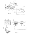
Fig. 1 is a perspective view of a remote I/O unit of a type suitable for use with the present invention showing a housing having multiple I/O modules contained therein for communication with an industrial process via terminals and a remote industrial controller via a network cable; -
Fig. 2 is a block diagram showing the I/O unit ofFig. 1 in the context of the industrial control system incorporating multiple remote I/O units and an industrial controller; -
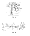
Fig. 3 is a block diagram of the remote I/O unit showing connectors for attaching I/O modules installed in the I/O unit to a common bus communicating with the network cable and electrical power, and showing one I/O module providing a power control circuit and a zero-crossing circuit controlled by a micro-controller; -
Fig. 4 is a detailed schematic of the zero-crossing circuit ofFig. 3 such as may receive an AC waveform from the output terminals to provide an isolated signal through an optical isolator; -
Fig. 5 is aligned graphs showing the AC waveform and the switching of the LED of the optical isolator for a short period of time only near the zero-crossing of the AC waveform; -
Fig. 6 is a plot of the state of switching of the LED of the optical isolator versus AC waveform voltage for the circuit ofFig. 4 ; and -
Fig. 7 is aligned graphs showing a change in the width of the pulse ofFig. 6 with different amplitudes of AC waveforms allowing indirect amplitude monitoring. - Referring now to
Figs. 1 and 2 , an I/O block 10 may provide for aunit housing 12 havingmultiple openings 14 for orienting and supporting corresponding replaceable or permanently installed I/O modules 16. The I/O modules 16 generally provide an electrical interface between anindustrial controller 17 and an industrial process ormachine 18, the latter havingactuators presenting loads 20 as powered by external field-side power sources 22 which may be AC sources (as shown) or DC sources as will be described. Each of the I/O modules 16 may have exposedscrew terminals 24 for connecting circuitry of the I/O module 16 viaelectrical conductors 26 to theload 20 and field-side power source 22 of the industrial process ormachine 18. - The
housing 12 of the I/O block 10 may be supported, for example, on aDIN rail 29 of a type known in the art or may provide for another mounting arrangement allowing it to be located close to the desired controlledloads 20. The I/O block 10 may connect via acontrol network 28, for example ControlNet or Ethernet IP, toindustrial controller 17 for communication of control data between the I/O modules 16 of the I/O block 10 and theindustrial controller 17. - Generally, the
industrial controller 17 will include at least oneprocessor 30 executing astored control program 32 contained in a communicatingmemory 34 to provide for communication with thecontrol network 28 to exchange signals with the I/O block 10 for control of the industrial process ormachine 18 according to astored control program 32. Thestored control program 32 reads signals indicating the state of the industrial process or machine 18 (from sensors or the like) and writes outputs to the I/O block 10 to control theloads 20 according to those sensed inputs and the logic of thecontrol program 32. Theindustrial controller 17 may include a connection to a user interface terminal 35 (for example including a display, computer, keyboard, and mouse or the like) allowing programming and other control of theindustrial controller 17 and providing for output of information to an operator.Industrial controllers 17 suitable for use with the present invention include, for example, programmable controllers commercially available from Rockwell Automation, Inc. - Generally, the I/
O modules 16 of each I/O block 10 include anelectrical isolation barrier 36 between the electrical power and circuitry of the industrial process ormachine 18 and directly connected portions of the I/O module 16, and the circuitry of the industrial control system including theindustrial controller 17, thenetwork 28, the I/O blocks 10 and remaining portions of the I/O modules 16. Electrical isolation, as understood herein, refers to the portions of an electrical circuit and do not communicate by a DC electric path within the I/O block 10. Circuitry on the side of theelectrical isolation barrier 36 toward the industrial process ormachine 18 will be termed "field-side" circuitry and circuitry on the side of the electrical isolation towards theindustrial controller 17 will be termed "controller-side" circuitry. Electrical isolation, as is understood in the art, may be accomplished by an optical isolator or transformer that prevents DC conduction through theelectrical isolation barrier 36 to prevent damage to the controller-side circuitry in the event of fault on the field-side circuitry. This isolation prevents simple sharing of electrical power between the circuits on the controller-side in the field-side by conductors spanning theisolation barrier 36. - Referring now to
Fig. 3 , each I/O block 10 may provide abackplane 40 providing a set of electrically releasable or permanently connectedelectrical connectors 42 communicating with abackplane bus 44 providing parallel or serial digital communication and electrical power. Electrical power may be provided by apower supply 43. The digital communication on thebackplane bus 44 may be moderated by aunit controller 46 includingnetwork circuit 45 communicating with theindustrial control network 28. Theunit controller 46 andnetwork circuit 45 may be, for example, one or more electronic processors executing a stored program stored in memory or the like. - The
electrical connectors 42 forming thebackplane bus 44 may connect with correspondingelectrical connectors 47 positioned at the rear of each I/O module 16 allowing electrical connection between controller-side circuitry of the I/O block 10 and the controller-side circuitry of the I/O module 16 for directly communicating data and power therebetween when an I/O module 16 is inserted into the I/O block 10. Within each I/O module 16, amodule controller 48, for example a microcontroller, may execute a storedprogram 50 to coordinate functions of the I/O module 16 by communicating withmultiple output circuits 52 and corresponding multiple zero-crossingdetector circuits 54. Each of theseoutput circuits 52 and zero-crossingdetector circuits 54 may provide internally for anelectrical isolation barrier 36 between controller-side and field-side circuitry as will be described. Each of theseoutput circuits 52 and zero-crossingdetector circuits 54 also communicate with a shared set of terminals 24 (only three shown for clarity) that may, for example, be screw type terminals releasably receivingelectrical conductors 26. - As will be understood in the art, the zero-crossing
detector circuit 54 provides a detection of zero-crossing of the waveform applied to theterminals 24 connected across an AC power line (the outer twoterminals 24 as depicted) to produce a zero-crossing signal 55 transmitted to themodule controller 48 and indicating the timing of the zero-crossing of AC waveform on theterminals 24. - The
module controller 48 receiving this zero-crossing signal 55 provides aswitch state signal 56 for eachoutput circuit 52 indicating a desired control of electrical power at an output terminal 24 (thecenter terminal 24 as depicted) based on theswitch state signal 56. In one mode of operation, conduction betweenoutput terminal 24 and oneother terminal 24 is changed byoutput circuit 52 via theswitch state signal 56 either by opening or closing the circuit betweenoutput terminals 24 and aline terminal 24 only at the zero-crossings of the AC waveform to: (1) reduce power dissipation in the internal switching elements used to control power conducted through theoutput terminals 24, (2) accommodate the architecture of the switching element characteristics (for example when a triac is used), and/or (3) reduce the generation of electromagnetic interference. - Alternatively, in a different mode of operation, the
module controller 48 may receive a switch command signal, for example, from thebackplane 40 as communicated from thecontroller 17, commanding a switching of conduction betweenterminals 24' and 24 at times other than zero-crossings of the AC waveform, for example, to provide for duty cycle control of the AC waveform. This latter mode of operation may control, for example, average current for a resistive heating element more precisely or may be used to deal with reactive loads. This phase offset control of the switching with respect to the zero-crossing signal may be implemented by appropriate instructions in the storedprogram 50. - Referring now to
Fig. 4 , the zero-crossingdetector circuit 54 may receive anAC waveform 60 across theterminals 24, for example aground reference 62 at one terminal 24' and the AC waveform atterminal 24. The AC waveform will, in one embodiment, be at approximately 60 Hz and have a voltage between 120 and 240 volts AC. - The terminal 24 receiving the AC waveform may connect to an
impedance element 64 comprising a series connectedinductor 66 andcapacitor 68 which in turn connects to the cathode of thezener diode 70 having its opposite terminal connected to ground 62. - The
zener diode 70 may have a relatively low zero zener voltage (e.g. five volts) providing a voltage drop across theimpedance element 64 of substantially the entire voltage of theAC waveform 60 when thezener diode 70 is conducting. For this reason,impedance element 64 must be sized to provide this necessary voltage drop and to limit current flow through thezener diode 72 and the acceptable value for that component, typically a few hundred milliamps or less. It will be understood that areactive impedance element 64 may block current flow without dissipating substantial energy in contrast to a blocking resistance so that substantially no heat is generated in this current limiting process. - The junction between the
impedance element 64 and thezener diode 70, being at the low zener regulated voltage, may connect to the anode of a rectifyingdiode 72 whose cathode connects to a filter capacitor 78, the latter connected between the cathode and ground. The combination of therectifier 72 and the filter capacitor 78 provide at their junction a source of regulated DC power toresistor 74 andresistor 76, both connected to that junction. -
Resistor 74 passes to the anode of a light emitting diode (LED) 80 being part of anoptical isolator 83. The cathode of theLED 80 connects in turn with the collector of anNPN switching transistor 82 whose emitter is connected to ground 62. When the switchingtransistor 82 is turned on, theLED 80 is illuminated providing optical signal 84 tophototransistor 86 of theoptical isolator 83 finding theisolation barrier 36. Thephototransistor 86 may be output as the zero-crossing signal 55, as described above, leading tomodule controller 48 shown inFig. 3 . -
Resistor 76, described above and also connected to the source of regulated DC power at the junction ofrectifier 72 and filter capacitor 78, provides regulated DC power to the emitter of afirst PNP transistor 90 and a collector of asecond NPN transistor 92. The collector ofPNP transistor 90 and the emitter ofNPN transistor 92 are both connected to ground and the bases of thetransistors high impedance resistance 94, the other end of which is attached to the terminal 24 receiving theAC waveform 60. Thisresistance 94 provides a trigger signal that is in phase with theAC waveform 60, avoiding the phase shift of theimpedance element 64. - The emitter of
PNP transistor 90 and collector ofNPN transistor 92 also join with the base of switchingtransistor 82 to provide abase voltage 91 such that switchingtransistor 82 will turn on (conduct current between its collector and emitter) only when bothtransistors transistors PNP transistor 90 andNPN transistor 92 are turned off, the emitter ofPNP transistor 90 and collector ofNPN transistor 92 will be retained at substantially 0.7 volts being the base to emitter forward bias voltage oftransistor 82 when both oftransistors - Referring now also to
Figs. 5 and 6 , when theAC waveform 60 connected betweenterminals 24 and 24' is at a voltage below zero volts,PNP transistor 90 will be turned on pulling thebase voltage 91 of switchingtransistor 82 to a low-voltage turning the switchingtransistor 82 off and stopping conduction of current through theLED 80. - When the
AC waveform 60 is between approximately zero and 0.7 volts,PNP transistor 90 will turn off andNPN transistor 92 will likewise be turned off again for lack of sufficient forward biasing of its emitter junction. At this time, thebase voltage 91 oftransistor 82 rises sufficiently to turn on switchingtransistor 82 andLED 80. - When the
AC waveform 60 rises above approximately 0.7 volts,PNP transistor 90 has its emitter back-biased and turns off but the emitter ofNPN transistor 92 is forward biased to turn on, again pullingbase voltage 91 close to ground by the saturation voltage ofNPN transistor 92 and turning off switchingtransistor 82. - Accordingly it will be understood that the switching
transistor 82 and theLED 80 are off for most of the cycle of the AC waveform substantially conserving power. Typically the duty cycle of thebase voltage 91 and hence of theLED 80 will be less than 10 percent and more typically much less than one percent of the period of theAC waveform 60. This reduced duty cycle provides less current drain of the power source provided by theimpedance element 64,rectifier 72, and filter capacitor 78 allowing these components to be comparably smaller and permitting a lowcurrent zener diode 70 to be used. - Referring now to
Fig. 7 , it will be understood that the width of the pulse ofwaveform 91 and hence of the output zero-crossing signal 55 can be used to determine a coarse voltage level of theAC waveform 60 within AC waveform. For example, when theAC waveform 60 is 240 volts, the zero-crossing will be steeper resulting in a relativelynarrow pulse 91 measured in absolute time. Conversely, when the AC waveform 60' is a relatively lower voltage, for example 120 volts, the zero-crossing will be slower extending the pulse of base voltage 90'. In this way, operation of the I/O module at 120 or 240 volts may be determined and other simple voltage measurements may be made. - Certain terminology is used herein for purposes of reference only, and thus is not intended to be limiting. For example, terms such as "upper", "lower", "above", and "below" refer to directions in the drawings to which reference is made. Terms such as "front", "back", "rear", "bottom" and "side", describe the orientation of portions of the component within a consistent but arbitrary frame of reference which is made clear by reference to the text and the associated drawings describing the component under discussion. Such terminology may include the words specifically mentioned above, derivatives thereof, and words of similar import. Similarly, the terms "first", "second" and other such numerical terms referring to structures do not imply a sequence or order unless clearly indicated by the context.
- When introducing elements or features of the present disclosure and the exemplary embodiments, the articles "a", "an", "the" and "said" are intended to mean that there are one or more of such elements or features. The terms "comprising", "including'" and "having" are intended to be inclusive and mean that there may be additional elements or features other than those specifically noted. It is further to be understood that the method steps, processes, and operations described herein are not to be construed as necessarily requiring their performance in the particular order discussed or illustrated, unless specifically identified as an order of performance. It is also to be understood that additional or alternative steps may be employed.
- References to "a microprocessor" and "a processor" or "the microprocessor" and "the processor," can be understood to include one or more microprocessors that can communicate in a stand-alone and/or a distributed environment(s), and can thus be configured to communicate via wired or wireless communications with other processors, where such one or more processor can be configured to operate on one or more processor-controlled devices that can be similar or different devices. Furthermore, references to memory, unless otherwise specified, can include one or more processor-readable and accessible memory elements and/or components that can be internal to the processor-controlled device, external to the processor-controlled device, and can be accessed via a wired or wireless network.
- Co-pending patent applications entitled Input Circuit For Industrial Control With Low Heat Dissipation serial number __________ and Output Module For Industrial Control With Sink And Source Capability And Low Heat Dissipation serial number __________ filed on even date herewith and assigned to the same assignee as the present invention are hereby incorporated by reference in their entirety.
- It is specifically intended that the present invention not be limited to the embodiments and illustrations contained herein and the claims should be understood to include modified forms of those embodiments including portions of the embodiments and combinations of elements of different embodiments as come within the scope of the following claims. All of the publications described herein, including patents and non-patent publications are hereby incorporated herein by reference in their entireties.
-
- Embodiment 1: An I/O module circuit for use in an industrial control system comprising:
- a housing;
- terminals supported by the housing for receipt of electrical power to be controlled by the I/O module circuit; and
- a circuit contained in the housing providing:
- a transistor switch element having an input connected to a terminal for receiving an AC waveform therefrom and having an output providing a zero-crossing signal indicating a voltage of the AC waveform within a first and second predetermined voltage threshold near zero voltage of the AC waveform;
- an optical isolator including a light emitting diode (LED) connected to the transistor switch element to switch on and off according to the zero-crossing signal and having a photosensitive solid-state switch receiving light from the LED to provide an optically isolated zero-crossing signal;
- wherein the zero-crossing signal from the transistor switch element provides conduction of the LED only during times when the AC waveform is between the first and second voltage threshold.
- Embodiment 2: The I/O module circuit of
embodiment 1 wherein the transistor switch element provides a duty cycle of less than five percent for AC waveforms in a range of 120 volts AC to 240 volts AC. - Embodiment 3. The I/O module circuit of embodiment 2 wherein the transistor switch element includes a first transistor that conducts when the AC waveform is above a first threshold and a second transistor that conducts when the AC waveform is below the second threshold and a third transistor communicating with the first and second transistors to conduct only when neither the first or second transistor is conducting.
- Embodiment 4: The I/O module circuit of embodiment 3 wherein the first transistor is an NPN transistor having a base connected to the AC waveform and the second transistor is a PNP transistor having a base connected to the AC waveform and wherein the NPN transistor and PNP transistor are connected in parallel to each other and in series with a resistance to a voltage provided by the power circuit and wherein the junction between the resistance and the parallel connected NPN and PNP transistors is connected to the base of the third transistor which controls current through the LED of the optical isolator.
- Embodiment 5: The I/O module circuit of
embodiment 1 wherein the transistor switch element is connected directly to the AC waveform through a resistance without rectification. - Embodiment 6: The I/O module circuit of
embodiment 1 further including a microprocessor for receiving the optically isolated zero-crossing signal and a switch element receiving a control signal from the microprocessor to control a switching of the AC waveform across the terminals. - Embodiment 7: The I/O module circuit of embodiment 6 wherein the microprocessor provides a switch signal at a predetermined phase delay with respect to an isolated zero-crossing signal according to a phase control signal received by the microprocessor.
- Embodiment 8: The I/O module circuit of
embodiment 1 further including a power circuit receiving the AC waveform to rectify the AC waveform to provide power to the transistor switch element. - Embodiment 9: The I/O module circuit of
embodiment 1 wherein the power receiving circuit includes a series connected nonresistance impedance limiting current to the power circuit. - Embodiment 10: The I/O module circuit of
embodiment 1 wherein the terminals are screw type terminals. - Embodiment 11: The I/O module circuit of
embodiment 1 further including a unit having multiple unit releasable electrical connectors, the units supporting multiple I/O module circuits each having releasable electrical connectors connecting with the unit releasable electrical connectors, the unit releasable electrical connectors further communicating with a network communication circuit for receiving the signal indicating a desired control of electrical power at the terminals of the I/O module from a remote industrial controller; wherein the unit includes elements for orienting and supporting the I/O module in the unit. - Embodiment 12: An industrial control system comprising:
- an industrial controller having at least one processor executing a stored program to receive input signals reflecting a state of a connected industrial process and to provide output signals providing desired control of the state of the connected industrial process;
- a network providing a protocol ensuring a guaranteed maximum delay in a communication of data on the network system communicating with the industrial controller to communicate input and output signals therewith;
- an I/O module communicating with the network system to exchange the input and output signals therewith, the I/O module further comprising:
- a housing;
- terminals supported by the housing for receipt of electrical power to be controlled by the I/O module circuit; and
- a circuit contained in the housing providing:
- a transistor switch element having an input connected to a terminal for receiving an AC waveform therefrom and having an output providing a zero-crossing signal indicating a voltage of the AC waveform within a first and second predetermined voltage threshold near zero voltage of the AC waveform;
- an optical isolator including a light emitting diode switched on and off according to the zero-crossing signal and having a photosensitive solid-state switch receiving light from the LED to provide an optically isolated zero-crossing signal;
- wherein the zero-crossing signal from the transistor switch element provides conduction of the LED only during times when the AC waveform is between the first and second voltage threshold.
- Embodiment 13: The industrial control system of
embodiment 12 wherein the transistor switch element provides a duty cycle of less than five percent for AC waveforms in the range of 120 volts AC to 240 volts AC. - Embodiment 14: The industrial control system of embodiment 13 wherein the transistor switch element includes a first transistor that conducts when the AC waveform is above a first threshold and a second transistor that conducts when the AC waveform is below the second threshold and a third transistor communicating with the first and second transistors to conduct only when neither the first or second transistor is conducting.
- Embodiment 15: The industrial control system of
embodiment 14 wherein the first transistor is an NPN transistor having a base connected to the AC waveform and the second transistor is a PNP transistor having a base connected to the AC waveform and wherein the NPN transistor and PNP transistor are connected in parallel to each other and in series with a resistance to a voltage provided by the power circuit and wherein the junction between the resistance and the parallel connected NPN and PNP transistors is connected to the base of the third transistor which controls current through the LED of the optical isolator. - Embodiment 16: The I/O module circuit of
embodiment 12 further including a microprocessor for receiving the optically isolated zero-crossing signal and a switch element receiving a control signal from the microprocessor to control a switching of the AC waveform across the terminals;
wherein the microprocessor provides a switch signal at a predetermined phase delay with respect to an isolated zero-crossing signal according to a phase control signal received by the microprocessor. - Embodiment 17: A method of switching an AC signal in an I/O module in an industrial control system comprising:
- receiving an AC waveform at terminals of the I/O module, at least one terminal communicating with a transistor switch element having an input connected to a terminal for receiving an AC waveform therefrom and having an output providing a zero-crossing signal indicating a voltage of the AC waveform within a first and second predetermined voltage threshold near zero voltage of the AC waveform;
- optically isolating the zero-crossing signal using an optical isolator including a light emitting diode switched on and off according to the zero-crossing signal and having a photosensitive solid-state switch receiving light from the LED to provide an optically isolated zero-crossing signal; and
- wherein the zero-crossing signal from the transistor switch element provides conduction of the LED only during times when the AC waveform is between the first and second voltage threshold.
Claims (15)
- An I/O module circuit for use in an industrial control system comprising:a housing;terminals supported by the housing for receipt of electrical power to be controlled by the I/O module circuit; anda circuit contained in the housing providing:a transistor switch element having an input connected to a terminal for receiving an AC waveform therefrom and having an output providing a zero-crossing signal indicating a voltage of the AC waveform within a first and second predetermined voltage threshold near zero voltage of the AC waveform;an optical isolator including a light emitting diode (LED) connected to the transistor switch element to switch on and off according to the zero-crossing signal and having a photosensitive solid-state switch receiving light from the LED to provide an optically isolated zero-crossing signal;wherein the zero-crossing signal from the transistor switch element provides conduction of the LED only during times when the AC waveform is between the first and second voltage threshold.
- The I/O module circuit of claim 1 wherein the transistor switch element provides a duty cycle of less than five percent for AC waveforms in a range of 120 volts AC to 240 volts AC.
- The I/O module circuit of claim 2 wherein the transistor switch element includes a first transistor that conducts when the AC waveform is above a first threshold and a second transistor that conducts when the AC waveform is below the second threshold and a third transistor communicating with the first and second transistors to conduct only when neither the first or second transistor is conducting.
- The I/O module circuit of claim 3 wherein the first transistor is an NPN transistor having a base connected to the AC waveform and the second transistor is a PNP transistor having a base connected to the AC waveform and wherein the NPN transistor and PNP transistor are connected in parallel to each other and in series with a resistance to a voltage provided by the power circuit and wherein the junction between the resistance and the parallel connected NPN and PNP transistors is connected to the base of the third transistor which controls current through the LED of the optical isolator.
- The I/O module circuit of any one of claims 1 to 4 wherein the transistor switch element is connected directly to the AC waveform through a resistance without rectification.
- The I/O module circuit of any one of claims 1 to 5 further including a microprocessor for receiving the optically isolated zero-crossing signal and a switch element receiving a control signal from the microprocessor to control a switching of the AC waveform across the terminals.
- The I/O module circuit of claim 6 wherein the microprocessor provides a switch signal at a predetermined phase delay with respect to an isolated zero-crossing signal according to a phase control signal received by the microprocessor.
- The I/O module circuit of any one of claims 1 to 7 further including a power circuit receiving the AC waveform to rectify the AC waveform to provide power to the transistor switch element.
- The I/O module circuit of any one of claims 1 to 8 wherein the power receiving circuit includes a series connected nonresistance impedance limiting current to the power circuit; or
wherein the terminals are screw type terminals. - The I/O module circuit of any one of claims 1 to 9 further including a unit having multiple unit releasable electrical connectors, the units supporting multiple I/O module circuits each having releasable electrical connectors connecting with the unit releasable electrical connectors, the unit releasable electrical connectors further communicating with a network communication circuit for receiving the signal indicating a desired control of electrical power at the terminals of the I/O module from a remote industrial controller; wherein the unit includes elements for orienting and supporting the I/O module in the unit.
- An industrial control system comprising:an industrial controller having at least one processor executing a stored program to receive input signals reflecting a state of a connected industrial process and to provide output signals providing desired control of the state of the connected industrial process;a network providing a protocol ensuring a guaranteed maximum delay in a communication of data on the network system communicating with the industrial controller to communicate input and output signals therewith;an I/O module communicating with the network system to exchange the input and output signals therewith, the I/O module further comprising:a housing;terminals supported by the housing for receipt of electrical power to be controlled by the I/O module circuit; anda circuit contained in the housing providing:a transistor switch element having an input connected to a terminal for receiving an AC waveform therefrom and having an output providing a zero-crossing signal indicating a voltage of the AC waveform within a first and second predetermined voltage threshold near zero voltage of the AC waveform;an optical isolator including a light emitting diode switched on and off according to the zero-crossing signal and having a photosensitive solid-state switch receiving light from the LED to provide an optically isolated zero-crossing signal;wherein the zero-crossing signal from the transistor switch element provides conduction of the LED only during times when the AC waveform is between the first and second voltage threshold.
- The industrial control system of claim 11 wherein the transistor switch element provides a duty cycle of less than five percent for AC waveforms in the range of 120 volts AC to 240 volts AC.
- The industrial control system of claim 12 wherein the transistor switch element includes a first transistor that conducts when the AC waveform is above a first threshold and a second transistor that conducts when the AC waveform is below the second threshold and a third transistor communicating with the first and second transistors to conduct only when neither the first or second transistor is conducting; and/or
wherein the first transistor is an NPN transistor having a base connected to the AC waveform and the second transistor is a PNP transistor having a base connected to the AC waveform and wherein the NPN transistor and PNP transistor are connected in parallel to each other and in series with a resistance to a voltage provided by the power circuit and wherein the junction between the resistance and the parallel connected NPN and PNP transistors is connected to the base of the third transistor which controls current through the LED of the optical isolator. - The I/O module circuit of any one of claims 11 to 13 further including a microprocessor for receiving the optically isolated zero-crossing signal and a switch element receiving a control signal from the microprocessor to control a switching of the AC waveform across the terminals;
wherein the microprocessor provides a switch signal at a predetermined phase delay with respect to an isolated zero-crossing signal according to a phase control signal received by the microprocessor. - A method of switching an AC signal in an I/O module in an industrial control system comprising:receiving an AC waveform at terminals of the I/O module, at least one terminal communicating with a transistor switch element having an input connected to a terminal for receiving an AC waveform therefrom and having an output providing a zero-crossing signal indicating a voltage of the AC waveform within a first and second predetermined voltage threshold near zero voltage of the AC waveform;optically isolating the zero-crossing signal using an optical isolator including a light emitting diode switched on and off according to the zero-crossing signal and having a photosensitive solid-state switch receiving light from the LED to provide an optically isolated zero-crossing signal; andwherein the zero-crossing signal from the transistor switch element provides conduction of the LED only during times when the AC waveform is between the first and second voltage threshold.
Applications Claiming Priority (1)
| Application Number | Priority Date | Filing Date | Title |
|---|---|---|---|
| US13/474,348 US8669787B2 (en) | 2012-05-17 | 2012-05-17 | Zero-crossing detector for industrial control with low heat dissipation |
Publications (3)
| Publication Number | Publication Date |
|---|---|
| EP2665182A2 true EP2665182A2 (en) | 2013-11-20 |
| EP2665182A3 EP2665182A3 (en) | 2014-10-15 |
| EP2665182B1 EP2665182B1 (en) | 2017-12-13 |
Family
ID=48470768
Family Applications (1)
| Application Number | Title | Priority Date | Filing Date |
|---|---|---|---|
| EP13168283.3A Active EP2665182B1 (en) | 2012-05-17 | 2013-05-17 | Zero-crossing detector for industrial control with low heat dissipation |
Country Status (3)
| Country | Link |
|---|---|
| US (1) | US8669787B2 (en) |
| EP (1) | EP2665182B1 (en) |
| CN (1) | CN103425095B (en) |
Cited By (5)
| Publication number | Priority date | Publication date | Assignee | Title |
|---|---|---|---|---|
| RU2547616C1 (en) * | 2014-04-18 | 2015-04-10 | Открытое акционерное общество "Научно-производственное предприятие "Пульсар" | On delay integrated circuit |
| CN107919867A (en) * | 2016-10-09 | 2018-04-17 | 华为技术有限公司 | Digital signal input circuit |
| WO2018129103A1 (en) * | 2017-01-03 | 2018-07-12 | Brilliant Home Technology, Inc. | Reversible-polarity wiring system |
| CN110389566A (en) * | 2018-04-23 | 2019-10-29 | 罗克韦尔自动化技术公司 | General purpose I/O industrial control module is provided |
| WO2022038148A1 (en) * | 2020-08-18 | 2022-02-24 | Weidmüller Interface GmbH & Co. KG | Device and method for detecting alternating voltage |
Families Citing this family (4)
| Publication number | Priority date | Publication date | Assignee | Title |
|---|---|---|---|---|
| US10254129B2 (en) | 2015-02-27 | 2019-04-09 | Infineon Technologies Ag | Low noise zero crossing detection for indirect tire pressure monitoring |
| EP3281268B1 (en) * | 2015-04-06 | 2023-11-22 | GE Aviation Systems LLC | Method for operating an electrical circuit |
| US10158358B2 (en) * | 2015-04-06 | 2018-12-18 | Rockwell Automation Technologies, Inc. | Low-power dissipation input circuit |
| US10670639B2 (en) * | 2017-02-21 | 2020-06-02 | Canon Kabushiki Kaisha | Apparatus for detecting alternating current zero cross and voltage |
Family Cites Families (12)
| Publication number | Priority date | Publication date | Assignee | Title |
|---|---|---|---|---|
| BE789423A (en) * | 1971-09-30 | 1973-03-28 | Westinghouse Electric Corp | ZERO PASSAGE DETECTOR |
| US5253140A (en) * | 1988-03-12 | 1993-10-12 | Fanuc Ltd. | Connector unit for input/output module of programmable controller having disengagement lever |
| US6662247B1 (en) * | 1999-11-30 | 2003-12-09 | Rockwell Automation Technologies, Inc. | Protocol for extended data transfer in scan-based industrial controller I/O system |
| US20080309379A1 (en) * | 2007-03-02 | 2008-12-18 | Carroll Sean C | Zero crossing circuit |
| US7508240B1 (en) * | 2007-04-06 | 2009-03-24 | Keithley Instruments, Inc. | Power mains zero-crossing detector |
| US7941229B2 (en) * | 2007-06-06 | 2011-05-10 | Rockwell Automation Technologies, Inc. | High-speed sequential sampling of I/O data for industrial control |
| US8446050B2 (en) * | 2009-12-17 | 2013-05-21 | Hamilton Sundstrand Corporation | Solid-state alternating current (AC) switch |
| US8248109B2 (en) * | 2010-01-11 | 2012-08-21 | Asco Power Technologies, L.P. | Methods and systems for detection of zero crossings in a signal |
| US7973562B1 (en) * | 2010-03-22 | 2011-07-05 | Rockwell Automation Technologies, Inc. | Universal sink/source I/O module for industrial controller |
| DE102010012529B3 (en) * | 2010-03-23 | 2011-06-09 | Theben Ag | Circuit arrangement for transmission of signals between electrical control circuit and load circuit for controlling and operation of opto-coupler, has NPN-transistor, whose base is connected to collector of PNP-transistor via base resistor |
| CN201926700U (en) * | 2010-11-03 | 2011-08-10 | 苏州合欣美电子科技有限公司 | Zero-crossing detection circuit |
| CN202196115U (en) * | 2011-09-08 | 2012-04-18 | 广州市金矢电子有限公司 | Voltage zero passage detection device and zero passage switching switch |
-
2012
- 2012-05-17 US US13/474,348 patent/US8669787B2/en active Active
-
2013
- 2013-05-17 EP EP13168283.3A patent/EP2665182B1/en active Active
- 2013-05-17 CN CN201310184313.2A patent/CN103425095B/en active Active
Non-Patent Citations (1)
| Title |
|---|
| None |
Cited By (8)
| Publication number | Priority date | Publication date | Assignee | Title |
|---|---|---|---|---|
| RU2547616C1 (en) * | 2014-04-18 | 2015-04-10 | Открытое акционерное общество "Научно-производственное предприятие "Пульсар" | On delay integrated circuit |
| CN107919867A (en) * | 2016-10-09 | 2018-04-17 | 华为技术有限公司 | Digital signal input circuit |
| WO2018129103A1 (en) * | 2017-01-03 | 2018-07-12 | Brilliant Home Technology, Inc. | Reversible-polarity wiring system |
| US10070499B2 (en) | 2017-01-03 | 2018-09-04 | Brilliant Home Technology, Inc. | Reversible-polarity wiring system |
| CN110291845A (en) * | 2017-01-03 | 2019-09-27 | 布里连特家居技术公司 | Can reversed polarity wiring system |
| CN110291845B (en) * | 2017-01-03 | 2020-06-09 | 布里连特家居技术公司 | Wiring system capable of reversing polarity |
| CN110389566A (en) * | 2018-04-23 | 2019-10-29 | 罗克韦尔自动化技术公司 | General purpose I/O industrial control module is provided |
| WO2022038148A1 (en) * | 2020-08-18 | 2022-02-24 | Weidmüller Interface GmbH & Co. KG | Device and method for detecting alternating voltage |
Also Published As
| Publication number | Publication date |
|---|---|
| CN103425095B (en) | 2016-08-24 |
| EP2665182B1 (en) | 2017-12-13 |
| CN103425095A (en) | 2013-12-04 |
| EP2665182A3 (en) | 2014-10-15 |
| US8669787B2 (en) | 2014-03-11 |
| US20130307586A1 (en) | 2013-11-21 |
Similar Documents
| Publication | Publication Date | Title |
|---|---|---|
| US8669787B2 (en) | Zero-crossing detector for industrial control with low heat dissipation | |
| EP2665188B1 (en) | Output module for industrial control with sink and source capability and low heat dissipation | |
| US7336463B2 (en) | Device and method for dimming service loads | |
| EP2665183B1 (en) | Input circuit for industrial control with low heat dissipation | |
| US10201064B1 (en) | Power supply for a two-wire smart dimmer and lighting loads thereof | |
| US11205964B2 (en) | Ground leakage power supply for dimming applications | |
| US20180102672A1 (en) | Lighting system including a power backup device | |
| US9888547B2 (en) | Circuit assembly for operating lighting means via a master-slave system | |
| KR101206386B1 (en) | Closed Circuit PLC system for large capacity load | |
| EP2739123A2 (en) | DALI power supply with reduced dissipation | |
| CN109921622B (en) | Circuit and system implementing a power supply configured for spark prevention | |
| EP1185909A1 (en) | An electronic means to sense actuation of ac output control circuitry | |
| US9685942B2 (en) | Circuit arrangement for the protection of at least one component of a two wire electrical current loop | |
| CN110168837B (en) | Lighting system comprising a power backup device | |
| CN110291845B (en) | Wiring system capable of reversing polarity | |
| US5925888A (en) | Optocoupler input expansion circuit | |
| JP7300636B2 (en) | LOAD CONTROL CIRCUIT, LOAD CONTROL METHOD, AND PROGRAM | |
| JP2011221588A (en) | Electronic equipment | |
| US9588154B2 (en) | Method for operating a microcomputer apparatus | |
| GB2556936A (en) | A switching system for an electrical appliance, a method of switching an electrical appliance and a lighting arrangement incorporating the switching system |
Legal Events
| Date | Code | Title | Description |
|---|---|---|---|
| PUAI | Public reference made under article 153(3) epc to a published international application that has entered the european phase |
Free format text: ORIGINAL CODE: 0009012 |
|
| AK | Designated contracting states |
Kind code of ref document: A2 Designated state(s): AL AT BE BG CH CY CZ DE DK EE ES FI FR GB GR HR HU IE IS IT LI LT LU LV MC MK MT NL NO PL PT RO RS SE SI SK SM TR |
|
| AX | Request for extension of the european patent |
Extension state: BA ME |
|
| REG | Reference to a national code |
Ref country code: DE Ref legal event code: R079 Ref document number: 602013030674 Country of ref document: DE Free format text: PREVIOUS MAIN CLASS: H03K0005080000 Ipc: H03K0005153600 |
|
| PUAL | Search report despatched |
Free format text: ORIGINAL CODE: 0009013 |
|
| AK | Designated contracting states |
Kind code of ref document: A3 Designated state(s): AL AT BE BG CH CY CZ DE DK EE ES FI FR GB GR HR HU IE IS IT LI LT LU LV MC MK MT NL NO PL PT RO RS SE SI SK SM TR |
|
| AX | Request for extension of the european patent |
Extension state: BA ME |
|
| RIC1 | Information provided on ipc code assigned before grant |
Ipc: H03K 5/1536 20060101AFI20140911BHEP |
|
| 17P | Request for examination filed |
Effective date: 20150414 |
|
| RBV | Designated contracting states (corrected) |
Designated state(s): AL AT BE BG CH CY CZ DE DK EE ES FI FR GB GR HR HU IE IS IT LI LT LU LV MC MK MT NL NO PL PT RO RS SE SI SK SM TR |
|
| GRAP | Despatch of communication of intention to grant a patent |
Free format text: ORIGINAL CODE: EPIDOSNIGR1 |
|
| INTG | Intention to grant announced |
Effective date: 20170822 |
|
| GRAS | Grant fee paid |
Free format text: ORIGINAL CODE: EPIDOSNIGR3 |
|
| GRAA | (expected) grant |
Free format text: ORIGINAL CODE: 0009210 |
|
| AK | Designated contracting states |
Kind code of ref document: B1 Designated state(s): AL AT BE BG CH CY CZ DE DK EE ES FI FR GB GR HR HU IE IS IT LI LT LU LV MC MK MT NL NO PL PT RO RS SE SI SK SM TR |
|
| REG | Reference to a national code |
Ref country code: GB Ref legal event code: FG4D |
|
| REG | Reference to a national code |
Ref country code: AT Ref legal event code: REF Ref document number: 955271 Country of ref document: AT Kind code of ref document: T Effective date: 20171215 Ref country code: CH Ref legal event code: EP |
|
| REG | Reference to a national code |
Ref country code: IE Ref legal event code: FG4D |
|
| REG | Reference to a national code |
Ref country code: DE Ref legal event code: R096 Ref document number: 602013030674 Country of ref document: DE |
|
| REG | Reference to a national code |
Ref country code: NL Ref legal event code: MP Effective date: 20171213 |
|
| REG | Reference to a national code |
Ref country code: LT Ref legal event code: MG4D |
|
| PG25 | Lapsed in a contracting state [announced via postgrant information from national office to epo] |
Ref country code: FI Free format text: LAPSE BECAUSE OF FAILURE TO SUBMIT A TRANSLATION OF THE DESCRIPTION OR TO PAY THE FEE WITHIN THE PRESCRIBED TIME-LIMIT Effective date: 20171213 Ref country code: LT Free format text: LAPSE BECAUSE OF FAILURE TO SUBMIT A TRANSLATION OF THE DESCRIPTION OR TO PAY THE FEE WITHIN THE PRESCRIBED TIME-LIMIT Effective date: 20171213 Ref country code: SE Free format text: LAPSE BECAUSE OF FAILURE TO SUBMIT A TRANSLATION OF THE DESCRIPTION OR TO PAY THE FEE WITHIN THE PRESCRIBED TIME-LIMIT Effective date: 20171213 Ref country code: NO Free format text: LAPSE BECAUSE OF FAILURE TO SUBMIT A TRANSLATION OF THE DESCRIPTION OR TO PAY THE FEE WITHIN THE PRESCRIBED TIME-LIMIT Effective date: 20180313 |
|
| REG | Reference to a national code |
Ref country code: AT Ref legal event code: MK05 Ref document number: 955271 Country of ref document: AT Kind code of ref document: T Effective date: 20171213 |
|
| REG | Reference to a national code |
Ref country code: FR Ref legal event code: PLFP Year of fee payment: 6 |
|
| PG25 | Lapsed in a contracting state [announced via postgrant information from national office to epo] |
Ref country code: BG Free format text: LAPSE BECAUSE OF FAILURE TO SUBMIT A TRANSLATION OF THE DESCRIPTION OR TO PAY THE FEE WITHIN THE PRESCRIBED TIME-LIMIT Effective date: 20180313 Ref country code: HR Free format text: LAPSE BECAUSE OF FAILURE TO SUBMIT A TRANSLATION OF THE DESCRIPTION OR TO PAY THE FEE WITHIN THE PRESCRIBED TIME-LIMIT Effective date: 20171213 Ref country code: LV Free format text: LAPSE BECAUSE OF FAILURE TO SUBMIT A TRANSLATION OF THE DESCRIPTION OR TO PAY THE FEE WITHIN THE PRESCRIBED TIME-LIMIT Effective date: 20171213 Ref country code: GR Free format text: LAPSE BECAUSE OF FAILURE TO SUBMIT A TRANSLATION OF THE DESCRIPTION OR TO PAY THE FEE WITHIN THE PRESCRIBED TIME-LIMIT Effective date: 20180314 Ref country code: RS Free format text: LAPSE BECAUSE OF FAILURE TO SUBMIT A TRANSLATION OF THE DESCRIPTION OR TO PAY THE FEE WITHIN THE PRESCRIBED TIME-LIMIT Effective date: 20171213 |
|
| PG25 | Lapsed in a contracting state [announced via postgrant information from national office to epo] |
Ref country code: NL Free format text: LAPSE BECAUSE OF FAILURE TO SUBMIT A TRANSLATION OF THE DESCRIPTION OR TO PAY THE FEE WITHIN THE PRESCRIBED TIME-LIMIT Effective date: 20171213 |
|
| PG25 | Lapsed in a contracting state [announced via postgrant information from national office to epo] |
Ref country code: CZ Free format text: LAPSE BECAUSE OF FAILURE TO SUBMIT A TRANSLATION OF THE DESCRIPTION OR TO PAY THE FEE WITHIN THE PRESCRIBED TIME-LIMIT Effective date: 20171213 Ref country code: ES Free format text: LAPSE BECAUSE OF FAILURE TO SUBMIT A TRANSLATION OF THE DESCRIPTION OR TO PAY THE FEE WITHIN THE PRESCRIBED TIME-LIMIT Effective date: 20171213 Ref country code: SK Free format text: LAPSE BECAUSE OF FAILURE TO SUBMIT A TRANSLATION OF THE DESCRIPTION OR TO PAY THE FEE WITHIN THE PRESCRIBED TIME-LIMIT Effective date: 20171213 Ref country code: EE Free format text: LAPSE BECAUSE OF FAILURE TO SUBMIT A TRANSLATION OF THE DESCRIPTION OR TO PAY THE FEE WITHIN THE PRESCRIBED TIME-LIMIT Effective date: 20171213 Ref country code: CY Free format text: LAPSE BECAUSE OF FAILURE TO SUBMIT A TRANSLATION OF THE DESCRIPTION OR TO PAY THE FEE WITHIN THE PRESCRIBED TIME-LIMIT Effective date: 20171213 |
|
| PG25 | Lapsed in a contracting state [announced via postgrant information from national office to epo] |
Ref country code: RO Free format text: LAPSE BECAUSE OF FAILURE TO SUBMIT A TRANSLATION OF THE DESCRIPTION OR TO PAY THE FEE WITHIN THE PRESCRIBED TIME-LIMIT Effective date: 20171213 Ref country code: IT Free format text: LAPSE BECAUSE OF FAILURE TO SUBMIT A TRANSLATION OF THE DESCRIPTION OR TO PAY THE FEE WITHIN THE PRESCRIBED TIME-LIMIT Effective date: 20171213 Ref country code: PL Free format text: LAPSE BECAUSE OF FAILURE TO SUBMIT A TRANSLATION OF THE DESCRIPTION OR TO PAY THE FEE WITHIN THE PRESCRIBED TIME-LIMIT Effective date: 20171213 Ref country code: AT Free format text: LAPSE BECAUSE OF FAILURE TO SUBMIT A TRANSLATION OF THE DESCRIPTION OR TO PAY THE FEE WITHIN THE PRESCRIBED TIME-LIMIT Effective date: 20171213 Ref country code: SM Free format text: LAPSE BECAUSE OF FAILURE TO SUBMIT A TRANSLATION OF THE DESCRIPTION OR TO PAY THE FEE WITHIN THE PRESCRIBED TIME-LIMIT Effective date: 20171213 Ref country code: IS Free format text: LAPSE BECAUSE OF FAILURE TO SUBMIT A TRANSLATION OF THE DESCRIPTION OR TO PAY THE FEE WITHIN THE PRESCRIBED TIME-LIMIT Effective date: 20180413 |
|
| REG | Reference to a national code |
Ref country code: DE Ref legal event code: R097 Ref document number: 602013030674 Country of ref document: DE |
|
| PLBE | No opposition filed within time limit |
Free format text: ORIGINAL CODE: 0009261 |
|
| STAA | Information on the status of an ep patent application or granted ep patent |
Free format text: STATUS: NO OPPOSITION FILED WITHIN TIME LIMIT |
|
| 26N | No opposition filed |
Effective date: 20180914 |
|
| PG25 | Lapsed in a contracting state [announced via postgrant information from national office to epo] |
Ref country code: DK Free format text: LAPSE BECAUSE OF FAILURE TO SUBMIT A TRANSLATION OF THE DESCRIPTION OR TO PAY THE FEE WITHIN THE PRESCRIBED TIME-LIMIT Effective date: 20171213 |
|
| REG | Reference to a national code |
Ref country code: CH Ref legal event code: PL |
|
| REG | Reference to a national code |
Ref country code: BE Ref legal event code: MM Effective date: 20180531 |
|
| PG25 | Lapsed in a contracting state [announced via postgrant information from national office to epo] |
Ref country code: MC Free format text: LAPSE BECAUSE OF FAILURE TO SUBMIT A TRANSLATION OF THE DESCRIPTION OR TO PAY THE FEE WITHIN THE PRESCRIBED TIME-LIMIT Effective date: 20171213 |
|
| REG | Reference to a national code |
Ref country code: IE Ref legal event code: MM4A |
|
| PG25 | Lapsed in a contracting state [announced via postgrant information from national office to epo] |
Ref country code: LI Free format text: LAPSE BECAUSE OF NON-PAYMENT OF DUE FEES Effective date: 20180531 Ref country code: SI Free format text: LAPSE BECAUSE OF FAILURE TO SUBMIT A TRANSLATION OF THE DESCRIPTION OR TO PAY THE FEE WITHIN THE PRESCRIBED TIME-LIMIT Effective date: 20171213 Ref country code: CH Free format text: LAPSE BECAUSE OF NON-PAYMENT OF DUE FEES Effective date: 20180531 |
|
| PG25 | Lapsed in a contracting state [announced via postgrant information from national office to epo] |
Ref country code: LU Free format text: LAPSE BECAUSE OF NON-PAYMENT OF DUE FEES Effective date: 20180517 |
|
| PG25 | Lapsed in a contracting state [announced via postgrant information from national office to epo] |
Ref country code: IE Free format text: LAPSE BECAUSE OF NON-PAYMENT OF DUE FEES Effective date: 20180517 |
|
| PG25 | Lapsed in a contracting state [announced via postgrant information from national office to epo] |
Ref country code: BE Free format text: LAPSE BECAUSE OF NON-PAYMENT OF DUE FEES Effective date: 20180531 |
|
| PG25 | Lapsed in a contracting state [announced via postgrant information from national office to epo] |
Ref country code: MT Free format text: LAPSE BECAUSE OF NON-PAYMENT OF DUE FEES Effective date: 20180517 |
|
| PG25 | Lapsed in a contracting state [announced via postgrant information from national office to epo] |
Ref country code: TR Free format text: LAPSE BECAUSE OF FAILURE TO SUBMIT A TRANSLATION OF THE DESCRIPTION OR TO PAY THE FEE WITHIN THE PRESCRIBED TIME-LIMIT Effective date: 20171213 |
|
| PG25 | Lapsed in a contracting state [announced via postgrant information from national office to epo] |
Ref country code: PT Free format text: LAPSE BECAUSE OF FAILURE TO SUBMIT A TRANSLATION OF THE DESCRIPTION OR TO PAY THE FEE WITHIN THE PRESCRIBED TIME-LIMIT Effective date: 20171213 Ref country code: HU Free format text: LAPSE BECAUSE OF FAILURE TO SUBMIT A TRANSLATION OF THE DESCRIPTION OR TO PAY THE FEE WITHIN THE PRESCRIBED TIME-LIMIT; INVALID AB INITIO Effective date: 20130517 |
|
| PG25 | Lapsed in a contracting state [announced via postgrant information from national office to epo] |
Ref country code: MK Free format text: LAPSE BECAUSE OF NON-PAYMENT OF DUE FEES Effective date: 20171213 |
|
| PG25 | Lapsed in a contracting state [announced via postgrant information from national office to epo] |
Ref country code: AL Free format text: LAPSE BECAUSE OF FAILURE TO SUBMIT A TRANSLATION OF THE DESCRIPTION OR TO PAY THE FEE WITHIN THE PRESCRIBED TIME-LIMIT Effective date: 20171213 |
|
| P01 | Opt-out of the competence of the unified patent court (upc) registered |
Effective date: 20230404 |
|
| PGFP | Annual fee paid to national office [announced via postgrant information from national office to epo] |
Ref country code: FR Payment date: 20230420 Year of fee payment: 11 Ref country code: DE Payment date: 20230419 Year of fee payment: 11 |
|
| PGFP | Annual fee paid to national office [announced via postgrant information from national office to epo] |
Ref country code: GB Payment date: 20230420 Year of fee payment: 11 |